THS6212
SBOS758E – MAY 2016 – REVISED MAY 2021
THS6212 Differential Broadband PLC Line Driver Amplifier
1 Features
3 Description
•
The THS6212 is a differential line-driver amplifier
with a current-feedback architecture. The device is
targeted for use in broadband, wideband power line
communications (PLC) line driver applications and is
fast enough to support transmissions of 14.5-dBm line
power up to 30 MHz.
•
•
•
•
•
•
•
•
•
Low power consumption:
– Full-bias mode: 23 mA
– Mid-bias mode: 17.5 mA
– Low-bias mode: 11.9 mA
– Low-power shutdown mode
– IADJ pin for variable bias
Low noise:
– Voltage noise: 2.5 nV/√Hz
– Inverting current noise: 18 pA/√Hz
– Noninverting current noise: 1.4 pA/√Hz
Low distortion:
– –86-dBc HD2 (1-MHz, 100-Ω
differential load)
– –101-dBc HD3 (1-MHz, 100-Ω differential load)
High output current: > 665 mA (25-Ω load)
Wide output swing:
– 49 VPP (28-V, 100-Ω differential load)
Wide bandwidth: 205 MHz (GDIFF = 10 V/V)
PSRR: >55 dB at 1 MHz for good isolation
Wide power-supply range: 10 V to 28 V
Thermal protection: 175°C (typical)
Alternative device with integrated common-mode
buffer: THS6222
2 Applications
•
•
The unique architecture of the THS6212 uses minimal
quiescent current and still achieves very high linearity.
Differential distortion under full bias conditions is –
86-dBc at 1 MHz and reduces to only –71 dBc
at 10 MHz. Fixed multiple bias settings allow for
enhanced power savings for line lengths where the
full performance of the amplifier is not required. To
allow for even more flexibility and power savings, an
adjustable current pin (IADJ) is available to further
lower the bias currents.
The wide output swing of 49 VPP (100-Ω differential
load) with 28-V power supplies, coupled with over
a 650-mA current drive (25-Ω load), allows for wide
dynamic headroom that keeps distortion minimal.
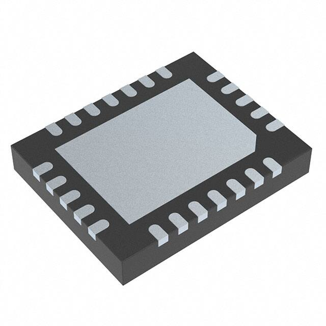
The THS6212 is available in a 24-pin VQFN package.
Device Information(1)
PART NUMBER
THS6212
High-voltage, high-current driving
Wide-band, power-line communications
(1)
PACKAGE
BODY SIZE (NOM)
VQFN (24)
5.00 mm × 4.00 mm
For all available packages, see the orderable addendum at
the end of the data sheet.
Vs+
R
S
D1
THS6212
R
T
R
F
R
P
R
G
100
R
�
P
R
F
R
S
D2
THS6212
I
ADJ
R
T
Vs-
Typical Line-Driver Circuit Using the THS6212
An IMPORTANT NOTICE at the end of this data sheet addresses availability, warranty, changes, use in safety-critical applications,
intellectual property matters and other important disclaimers. PRODUCTION DATA.
�THS6212
www.ti.com
SBOS758E – MAY 2016 – REVISED MAY 2021
Table of Contents
1 Features............................................................................1
2 Applications..................................................................... 1
3 Description.......................................................................1
4 Revision History.............................................................. 2
5 Pin Configuration and Functions...................................5
6 Specifications.................................................................. 6
6.1 Absolute Maximum Ratings ....................................... 6
6.2 ESD Ratings .............................................................. 6
6.3 Recommended Operating Conditions ........................6
6.4 Thermal Information ...................................................6
6.5 Electrical Characteristics: VS = 12 V .......................... 7
6.6 Electrical Characteristics: VS = 28 V .......................... 9
6.7 Timing Requirements ............................................... 10
6.8 Typical Characteristics: VS = 12 V.............................11
6.9 Typical Characteristics: VS = 28 V............................ 17
7 Detailed Description......................................................20
7.1 Overview................................................................... 20
7.2 Functional Block Diagram......................................... 20
7.3 Feature Description...................................................20
7.4 Device Functional Modes..........................................24
8 Application and Implementation.................................. 25
8.1 Application Information............................................. 25
8.2 Typical Applications.................................................. 25
8.3 What To Do and What Not to Do...............................31
9 Power Supply Recommendations................................31
10 Layout...........................................................................32
10.1 Layout Guidelines................................................... 32
10.2 Layout Example...................................................... 34
11 Device and Documentation Support..........................36
11.1 Documentation Support.......................................... 36
11.2 Receiving Notification of Documentation Updates.. 36
11.3 Support Resources................................................. 36
11.4 Trademarks............................................................. 36
11.5 Electrostatic Discharge Caution.............................. 36
11.6 Glossary.................................................................. 36
12 Mechanical, Packaging, and Orderable
Information.................................................................... 36
4 Revision History
NOTE: Page numbers for previous revisions may differ from page numbers in the current version.
Changes from Revision D (Novermber 2019) to Revision E (May 2021)
Page
• Updated the numbering format for tables, figures, and cross-references throughout the document..................1
• Changed mid-bias mode value from 17.7 mA to 17.5 mA in Features list .........................................................1
• Changed low-bias mode value from 12.2 mA to 11.9 mA in Features list ......................................................... 1
• Changed voltage noise value from 2.7 nV/√ Hz to 2.5 nV/√ Hz in Features list ................................................ 1
• Changed inverting current noise value from 17 pA/√ Hz to 18 pA/√ Hzin Features list ..................................... 1
• Changed noninverting current noise value from 1.2 pA/√ Hz to 1.4 pA/√ Hzin Features list ............................. 1
• Changed HD2 distortion from -100 dBc to -86 dBc in Features list ................................................................... 1
• Changed HD3 distortion from -89 dBc -101 dBc inFeatures list ........................................................................ 1
• Changed output current from > 416 mA to > 665 mA in Features list ............................................................... 1
• Changed output swing from 43.2 Vpp to 49 Vpp in Features list .......................................................................1
• Changed bandwidth from 150 MHz to 205 MHz in Features list ....................................................................... 1
• Changed PSRR from 50 dB to > 55 dB in Features list .....................................................................................1
• Changed thermal protection from 170°C to 175°C in Features list ....................................................................1
• Changed differential distortion to HD2 and updated values in Description section............................................ 1
• Changed output swing from 43.2Vpp to 49Vpp in Description section...............................................................1
• Changed power supplies from ± 12-V to 28-V in Description section.................................................................1
• Changed current drive from 416-mA to 650-mA in Description section..............................................................1
• Removed YS bond pad package from document............................................................................................... 1
• Changed Typical Line-Driver Circuit Using the THS6212 figure......................................................................... 1
• Removed YS die package and Bond Pad Functions table................................................................................. 5
• Deleted Output current, IO from Absolute Maximum Ratings.............................................................................6
• Added Bias control pin voltage in Absolute Maximum Ratings ..........................................................................6
• Added Input voltage to all pins except VS+, VS-, and BIAS control in Absolute Maximum Ratings ..................6
• Added Input current limit in Absolute Maximum Ratings ................................................................................... 6
• Changed Maximum junction, TJ from 130 C to 125 C in Absolute Maximum Ratings ...................................... 6
• Deleted ESD MM in ESD Ratings ......................................................................................................................6
• Changed Operating junction temperature from 130°C to 125°C in Recommended Operating Conditions........ 6
• Added Minimum ambient operating air temperature spec in Recommended Operating Conditions ................. 6
• Changed RΘJA from 33.2 °C/W to 42.3 °C/W in Thermal Information ............................................................... 6
2
Submit Document Feedback
Copyright © 2022 Texas Instruments Incorporated
Product Folder Links: THS6212
�THS6212
www.ti.com
•
•
•
•
•
•
•
•
•
•
•
•
•
•
•
•
•
•
•
•
•
•
•
•
•
•
•
•
•
•
•
•
•
•
•
•
•
•
•
•
•
•
•
•
•
•
•
SBOS758E – MAY 2016 – REVISED MAY 2021
Changed RΘJC(Top) from 31.7 °C/W to 32.8 °C/W in Thermal Information ......................................................... 6
Changed RΘJB from 11.3 °C/W to 20.9 °C/W in Thermal Information ................................................................6
Changed ψJT from 0.4 °C/W to 3.8 °C/W in Thermal Information ......................................................................6
Changed ψJB from 11.3 °C/W to 20.9 °C/W in Thermal Information ..................................................................6
Changed ψJC(bot) from 3.9 °C/W to 9.5 °C/W in Thermal Information ................................................................6
Added Electrical Characteristics: VS = 12V table................................................................................................7
Deleted Electrical Characteristics: VS = ±6 V table............................................................................................ 7
Added Electrical Characteristics: VS = 28V table .............................................................................................. 9
Deleted Deleted Electrical Characteristics: VS = ±12 V table.............................................................................9
Changed tON from 1µs to 25ns in Timing Requirements ................................................................................. 10
Changed tOFF from 1µs to 275ns in Timing Requirements .............................................................................. 10
Added Typical Characteristics: VS = 12 V......................................................................................................... 11
Deleted Typical Characteristics: VS = ±6 V (Full Bias)......................................................................................11
Deleted Typical Characteristics: VS = ±6 V (Mid Bias)......................................................................................11
Deleted Typical Characteristics: VS = ±6 V (Low Bias)..................................................................................... 11
Added Typical Characteristics: VS = 28 V.........................................................................................................17
Deleted Typical Characteristics: VS = ±12 V (Full Bias)....................................................................................17
Deleted Typical Characteristics: VS = ±12 V (Mid Bias)....................................................................................17
Deleted Typical Characteristics: VS = ±12 V (Low Bias)...................................................................................17
Changed output swing from 43.2 Vpp to 49 Vpp in Overview section..............................................................20
Changed current drive from 416 mA to 650 mA in Overview section............................................................... 20
Changed thermal protection junction temperature from 170°C to 175°C in Overview section......................... 20
Deleted Output Current and Voltage section.................................................................................................... 20
Added Output Voltage and Current Drive section.............................................................................................20
Changed referenced figures for RS versus capacitive load in Driving Capacitive Loads section..................... 21
Changed ±12-V supplies to 28-V supply in Distortion Performance section.................................................... 22
Changed ±6-V supplies to 12-V supply in Distortion Performance section...................................................... 22
Changed noise evaluation from Section 8.2.2 to Figure 8-1 in Differential Noise Performance section.......... 22
Added RS = 50 Ω in Differential Noise Performance section............................................................................ 22
Changed 38.9 nV/√ Hz calculation to 53.3 nV/√ Hz in Differential Noise Performance section....................... 22
Changed 7 nV/√ Hz calculation to 6.5 nV/√ Hz in Differential Noise Performance section.............................. 22
Changed output offset calculation to typical rather than worst case in DC Accuracy and Offset Control section
..........................................................................................................................................................................24
Changed quiescent current value from 23 mA to 19.5 mA in Wideband Current-Feedback Operation section...
25
Changed swing from 1.9 V from either rail to 49 Vpp in Wideband Current-Feedback Operation section.......25
Changed current drive from 416 mA to 650 mA inWideband Current-Feedback Operation section................ 25
Changed ± 6 V supply to 28 V supply inWideband Current-Feedback Operation section............................... 25
Changed 140 MHz bandwidth to 285 MHz inWideband Current-Feedback Operation section........................25
Changed Noninverting Differential I/O Amplifierfigure inWideband Current-Feedback Operation section.......25
Changed Frequency Response and Harmonic Distortion figures in Application Curves section..................... 26
Changed Dual-Supply Downstream Driver figure.............................................................................................27
Changed supply voltages to ±14 V in Line Driver Headroom Requirements section....................................... 28
Changed quiescent current value from 23 mA to 19.5 mA and ±12 V to ±14 V in Computing Total Driver
Power for Line-Driving Applications .................................................................................................................30
Changed 23 mA to 19.5 mA, 24 V to 28 V and 1003 mW to 11 mW in Computing Total Driver Power for LineDriving Applications ......................................................................................................................................... 30
Changed supply range from "±5 V to ±14 V" to "10 V to 28 V" in Power Supply Recommendations section.. 31
Changed referenced figures for RS versus capacitive load in Driving Capacitive Loads section..................... 32
Deleted Wafer and Die Information section...................................................................................................... 32
Changed ±12-V to 28-V in Layout Guidelines section...................................................................................... 32
Changes from Revision C (May 2016) to Revision D (Novermber 2019)
Page
• Added last two Features bullets .........................................................................................................................1
• Added last paragraph to Overview section ...................................................................................................... 20
Submit Document Feedback
Copyright © 2022 Texas Instruments Incorporated
Product Folder Links: THS6212
3
�THS6212
www.ti.com
SBOS758E – MAY 2016 – REVISED MAY 2021
•
4
Changed Dual-Supply Downstream Driver figure.............................................................................................27
Submit Document Feedback
Copyright © 2022 Texas Instruments Incorporated
Product Folder Links: THS6212
�THS6212
www.ti.com
SBOS758E – MAY 2016 – REVISED MAY 2021
BIAS-2
BIAS-1
VS–
VS+
D1_OUT
24
23
22
21
20
5 Pin Configuration and Functions
D1_IN+
1
19
D1_FB
D2_IN+
2
18
D2_FB
GND
3
17
D2_OUT
16
NC
Thermal
IADJ
4
NC
5
15
NC
NC
6
14
NC
NC
7
13
NC
8
9
10
11
12
NC
NC
NC
NC
NC
Pad
NC = no internal connection.
Figure 5-1. RHF Package 24-Pin VQFN With Exposed Thermal Pad Top View
Table 5-1. Pin Functions(1)
PIN
I/O
DESCRIPTION
NAME
NO.
BIAS-1
23
I
Bias mode parallel control, LSB
BIAS-2
24
I
Bias mode parallel control, MSB
D1_FB
19
I
Amplifier D1 inverting input
D2_FB
18
I
Amplifier D2 inverting input
D1_IN+
1
I
Amplifier D1 noninverting input
D2_IN+
2
I
Amplifier D2 noninverting input
D1_OUT
20
O
Amplifier D1 output
D2_OUT
17
O
Amplifier D2 output
GND(2)
3
I/O
Control pin ground reference
IADJ
4
I/O
Bias current adjustment pin
NC
5-16
—
No internal connection
VS–
22
I/O
Negative power-supply connection
VS+
21
I/O
Positive power-supply connection
(1)
(2)
The THS6212 defaults to the shutdown (disable) state if a signal is not present on the bias pins.
The GND pin ranges from VS– to (VS+ – 5 V).
Submit Document Feedback
Copyright © 2022 Texas Instruments Incorporated
Product Folder Links: THS6212
5
�THS6212
www.ti.com
SBOS758E – MAY 2016 – REVISED MAY 2021
6 Specifications
6.1 Absolute Maximum Ratings
over operating free-air temperature range (unless otherwise noted)(1)
MIN
MAX
28
V
0
14.5
V
(VS–) – 0.5
(VS+) + 0.5
V
±2
V
±10
mA
Supply voltage, VS = (VS+) – (VS–)
Voltage
Bias control pin voltage, referenced to GND pin
All pins except VS+, VS–, and BIAS control
Differential input voltage (each amplifier), VID
Current
All input pins, current limit
Continuous power dissipation(2)
Temperature
See Thermal Information table
Maximum junction, TJ (under any condition)(3)
150
Maximum junction, TJ (continuous operation, long-term reliability)(4)
125
Storage, Tstg
(1)
(2)
(3)
(4)
UNIT
–65
°C
150
Stresses beyond those listed under Absolute Maximum Rating may cause permanent damage to the device. These are stress
ratings only, which do not imply functional operation of the device at these or any other conditions beyond those indicated
under Recommended Operating Condition. Exposure to absolute-maximum-rated conditions for extended periods may affect device
reliability.
The THS6212 incorporates a thermal pad on the underside of the device. This pad functions as a heatsink and must be connected to
a thermally dissipating plane for proper power dissipation. Failure to do so can result in exceeding the maximum junction temperature,
which can permanently damage the device.
The absolute maximum junction temperature under any condition is limited by the constraints of the silicon process.
The absolute maximum junction temperature for continuous operation is limited by the package constraints. Operation above this
temperature can result in reduced reliability or lifetime of the device
6.2 ESD Ratings
VALUE
V(ESD)
(1)
(2)
Electrostatic
discharge
Human body model (HBM), per ANSI/ESDA/JEDEC JS-001, all pins(1)
±2000
Charged device model (CDM), per JEDEC specification JESD22-C101, all pins(2)
±500
UNIT
V
JEDEC document JEP155 states that 500-V HBM allows safe manufacturing with a standard ESD control process.
JEDEC document JEP157 states that 250-V CDM allows safe manufacturing with a standard ESD control process.
6.3 Recommended Operating Conditions
over operating free-air temperature range (unless otherwise noted)
MIN
VS
Supply voltage, VS = (VS+) – (VS–)
GND
GND pin voltage
TJ
Operating junction temperature
TA
Ambient operating air temperature
NOM
MAX
UNIT
10
28
V
VS–
VS+ – 5
V
125
°C
85
°C
–40
25
6.4 Thermal Information
THS6212
THERMAL METRIC(1)
RHF (VQFN)
UNIT
24 PINS
6
RθJA
Junction-to-ambient thermal resistance
42.3
°C/W
RθJC(top)
Junction-to-case (top) thermal resistance
32.8
°C/W
RθJB
Junction-to-board thermal resistance
20.9
°C/W
ΨJT
Junction-to-top characterization parameter
3.8
°C/W
YJB
Junction-to-board characterization parameter
20.9
°C/W
Submit Document Feedback
Copyright © 2022 Texas Instruments Incorporated
Product Folder Links: THS6212
�THS6212
www.ti.com
SBOS758E – MAY 2016 – REVISED MAY 2021
6.4 Thermal Information (continued)
THS6212
THERMAL
METRIC(1)
UNIT
RHF (VQFN)
24 PINS
RθJC(bot)
(1)
Junction-to-case (bottom) thermal resistance
9.5
°C/W
For more information about traditional and new thermal metrics, see the Semiconductor and IC Package Thermal Metrics application
report.
6.5 Electrical Characteristics: VS = 12 V
at TA ≈ 25°C, differential closed-loop gain (AV) = 10 V/V, differential load (RL) = 50 Ω, series isolation resistor (RS) = 2.5 Ω
each, RF = 1.24 kΩ, RADJ = 0 Ω, VO = D1_OUT – D2_OUT, and full bias (unless otherwise noted)
PARAMETER
TEST CONDITIONS
MIN
TYP
MAX
UNIT
AC PERFORMANCE
SSBW
Small-signal bandwidth
AV = 5 V/V, RF = 1.5 kΩ, VO = 2 VPP
250
AV = 10 V/V, RF = 1.24 kΩ, VO = 2 VPP
180
AV = 15 V/V, RF = 1 kΩ, VO = 2 VPP
165
0.1-dB bandwidth flatness
LSBW
Large-signal bandwidth
VO = 16 VPP
SR
Slew rate (20% to 80%)
VO = 16-V step
Rise and fall time (10% to 90%)
VO = 2 VPP
HD2
HD3
2nd-order harmonic distortion
3rd-order harmonic distortion
AV = 10 V/V,
VO = 2 VPP,
RL = 50 Ω
AV = 10 V/V,
VO = 2 VPP,
RL = 50 Ω
MHz
17
MHz
195
MHz
5500
V/µs
2.1
Full bias, f = 1 MHz
–80
Mid bias, f = 1 MHz
–78
Low bias, f = 1 MHz
–78
Full bias, f = 10 MHz
–61
Mid bias, f = 10 MHz
–61
Low bias, f = 10 MHz
–61
Full bias, f = 1 MHz
–90
Mid bias, f = 1 MHz
–86
Low bias, f = 1 MHz
–83
Full bias, f = 10 MHz
–69
Mid bias, f = 10 MHz
–65
Low bias, f = 10 MHz
–62
ns
dBc
dBc
en
Differential input voltage noise
f ≥ 1 MHz, input-referred
2.5
nV/√Hz
in+
Noninverting input current noise
f ≥ 1 MHz, each amplifier
1.4
pA/√Hz
in-
Inverting input current noise
f ≥ 1 MHz, each amplifier
18
pA/√Hz
DC PERFORMANCE
ZOL
Open-loop transimpedance gain
1300
kΩ
±12
Input offset voltage (each amplifier)
TA = –40°C
±16
TA = 85°C
±11
mV
±1
Noninverting input bias current
TA = –40°C
±1
TA = 85°C
±1
µA
±8
Inverting input bias current
TA = –40°C
±7
TA = 85°C
±4
µA
INPUT CHARACTERISTICS
Submit Document Feedback
Copyright © 2022 Texas Instruments Incorporated
Product Folder Links: THS6212
7
�THS6212
www.ti.com
SBOS758E – MAY 2016 – REVISED MAY 2021
6.5 Electrical Characteristics: VS = 12 V (continued)
at TA ≈ 25°C, differential closed-loop gain (AV) = 10 V/V, differential load (RL) = 50 Ω, series isolation resistor (RS) = 2.5 Ω
each, RF = 1.24 kΩ, RADJ = 0 Ω, VO = D1_OUT – D2_OUT, and full bias (unless otherwise noted)
PARAMETER
Common-mode input range
CMRR
Common-mode rejection ratio
TEST CONDITIONS
MIN
Each input with respect to midsupply
TYP
MAX
±3.0
Each input
64
TA = –40°C
67
TA = 85°C
62
Noninverting differential input
resistance
V
dB
10 || 2
Inverting input resistance
UNIT
kΩ || pF
43
Ω
OUTPUT CHARACTERISTICS
VO
Output voltage swing
IO
Output current (sourcing and sinking)
RL = 100 Ω, RS = 0 Ω
±9.7
RL = 50 Ω, RS = 0 Ω
±9.3
RL = 25 Ω, RS = 0 Ω
±8.4
RL = 25 Ω, RS = 0 Ω, based on
VO specification
±338
mA
±0.81
A
0.03
Ω
Short-circuit output current
ZO
Closed-loop output impedance
f = 1 MHz, differential
V
POWER SUPPLY
VS
Operating voltage
GND
GND pin voltage
10
TA = –40°C to +85°C
VS–
Full bias (BIAS-1 = 0, BIAS-2 = 0)
IS+
Quiescent current
IS–
Quiescent current
12
10
28
28
0
VS+ – 5
V
V
19.5
Mid bias (BIAS-1 = 1, BIAS-2 = 0)
15
Low bias (BIAS-1 = 0, BIAS-2 = 1)
10.4
Bias off (BIAS-1 = 1, BIAS-2 = 1)
0.8
Full bias (BIAS-1 = 0, BIAS-2 = 0)
18.8
Mid bias (BIAS-1 = 1, BIAS-2 = 0)
14.4
Low bias (BIAS-1 = 0, BIAS-2 = 1)
9.6
mA
mA
Bias off (BIAS-1 = 1, BIAS-2 = 1)
0.01
Current through GND pin
Full bias (BIAS-1 = 0, BIAS-2 = 0)
0.8
mA
+PSRR
Positive power-supply rejection ratio
Differential
83
dB
–PSRR
Negative power-supply rejection ratio
Differential
83
dB
BIAS CONTROL
Bias control pin voltage range
Bias control pin logic threshold
Bias control pin current(1)
Open-loop output impedance
(1)
8
With respect to GND pin,
TA = –40°C to +85°C
Logic 1, with respect to GND pin,
TA = –40°C to +85°C
0
3.3
V
2.1
V
Logic 0, with respect to GND pin,
TA = –40°C to +85°C
0.8
BIAS-1, BIAS-2 = 0.5 V (logic 0)
–9.6
BIAS-1, BIAS-2 = 3.3 V (logic 1)
0.3
Off bias (BIAS-1 = 1, BIAS-2 = 1)
12
70 || 5
1
µA
MΩ || pF
Current is considered positive out of the pin.
Submit Document Feedback
Copyright © 2022 Texas Instruments Incorporated
Product Folder Links: THS6212
�THS6212
www.ti.com
SBOS758E – MAY 2016 – REVISED MAY 2021
6.6 Electrical Characteristics: VS = 28 V
at TA ≈ 25°C, differential closed-loop gain (AV) = 10 V/V, differential load (RL) = 100 Ω, RF = 1.24 kΩ, RADJ = 0 Ω, VO =
D1_OUT – D2_OUT, and full bias (unless otherwise noted)
PARAMETER
TEST CONDITIONS
MIN
TYP
MAX
UNIT
AC PERFORMANCE
SSBW
Small-signal bandwidth, –3 dB
AV = 5 V/V, RF = 1.5 kΩ, VO = 2 VPP
285
AV = 10 V/V, RF = 1.24 kΩ, VO = 2 VPP
205
13
MHz
170
MHz
11,000
V/µs
0.1-dB bandwidth flatness
LSBW
Large-signal bandwidth
VO = 40 VPP
SR
Slew rate (20% to 80% level)
VO = 40-V step
Rise and fall time
VO = 2 VPP
HD2
2nd-order harmonic distortion
AV = 10 V/V,
VO = 2 VPP,
RL = 100 Ω
2
Full bias, f = 1 MHz
–86
Low bias, f = 1 MHz
–79
Full bias, f = 10 MHz
–71
Low bias, f = 10 MHz
–101
Low bias, f = 1 MHz
–88
Full bias, f = 10 MHz
–80
Low bias, f = 10 MHz
–65
3rd-order harmonic distortion
AV = 10 V/V,
VO = 2 VPP,
RL = 100 Ω
en
Differential input voltage noise
f ≥ 1 MHz, input-referred
in+
in-
ns
dBc
–63
Full bias, f = 1 MHz
HD3
MHz
dBc
2.5
nV/√Hz
Noninverting input current noise (each
f ≥ 1 MHz
amplifier)
1.7
pA/√Hz
Inverting input current noise (each
amplifier)
18
pA/√Hz
f ≥ 1 MHz
DC PERFORMANCE
ZOL
Open-loop transimpedance gain
1500
Input offset voltage
kΩ
±12
mV
Input offset voltage drift
TA = –40°C to +85°C
–40
µV/°C
Input offset voltage matching
Amplifier A to B
±0.5
mV
Noninverting input bias current
±1
µA
Inverting input bias current
±6
µA
Inverting input bias current matching
±8
µA
±10
V
INPUT CHARACTERISTICS
CMRR
Common-mode input range
Each input
±9
Common-mode rejection ratio
Each input
53
Noninverting input resistance
65
10 || 2
Inverting input resistance
38
dB
kΩ || pF
Ω
OUTPUT CHARACTERISTICS
VO
Output voltage swing(1)
IO
(1)
Output current (sourcing and sinking)
RL = 100 Ω
±24.5
RL = 25 Ω
±12.3
RL = 25 Ω, based on VO specification
Short-circuit output current
ZO
Output impedance
f = 1 MHz, differential
±580
±665
V
mA
1
A
0.01
Ω
Submit Document Feedback
Copyright © 2022 Texas Instruments Incorporated
Product Folder Links: THS6212
9
�THS6212
www.ti.com
SBOS758E – MAY 2016 – REVISED MAY 2021
6.6 Electrical Characteristics: VS = 28 V (continued)
at TA ≈ 25°C, differential closed-loop gain (AV) = 10 V/V, differential load (RL) = 100 Ω, RF = 1.24 kΩ, RADJ = 0 Ω, VO =
D1_OUT – D2_OUT, and full bias (unless otherwise noted)
PARAMETER
TEST CONDITIONS
MIN
TYP
MAX
10
12
28
UNIT
POWER SUPPLY
VS
Operating voltage
IS+
Quiescent current
IS–
Quiescent current
TA = –40°C to +85°C
10
28
Full bias (BIAS-1 = 0, BIAS-2 = 0)
23
Mid bias (BIAS-1 = 1, BIAS-2 = 0)
17.5
Low bias (BIAS-1 = 0, BIAS-2 = 1)
11.9
Bias off (BIAS-1 = 1, BIAS-2 = 1)
1.1
Full bias (BIAS-1 = 0, BIAS-2 = 0)
22
Mid bias (BIAS-1 = 1, BIAS-2 = 0)
16.4
Low bias (BIAS-1 = 0, BIAS-2 = 1)
10.8
Bias off (BIAS-1 = 1, BIAS-2 = 1)
Current through GND pin
Full bias (BIAS-1 = 0, BIAS-2 = 0)
+PSRR
Positive power-supply rejection ratio
–PSRR
Negative power-supply rejection ratio
0.1
V
mA
1.3
mA
0.8
1
mA
Differential
83
dB
Differential
77
dB
BIAS CONTROL
Bias control pin range
Bias control pin logic threshold
Bias control pin current(2)
(1)
(2)
With respect to GND pin,
TA = –40°C to +85°C
Logic 1, with respect to GND pin,
TA = –40°C to +85°C
0
3.3
V
1.9
V
Logic 0, with respect to GND pin,
TA = –40°C to +85°C
BIAS-1, BIAS-2 = 0.5 V (logic 0)
14.5
0.8
–15
BIAS-1, BIAS-2 = 3.3 V (logic 1)
–10
0.1
1
NOM
MAX
µA
See Section 7.3.1 for output voltage vs output current characteristics.
Current is considered positive out of the pin.
6.7 Timing Requirements
MIN
UNIT
tON
Turnon time delay: time for output to start tracking the input
25
ns
tOFF
Turnoff time delay: time for output to stop tracking the input
275
ns
10
Submit Document Feedback
Copyright © 2022 Texas Instruments Incorporated
Product Folder Links: THS6212
�THS6212
www.ti.com
SBOS758E – MAY 2016 – REVISED MAY 2021
6.8 Typical Characteristics: VS = 12 V
3
3
0
0
Normalized Gain (dB)
Normalized Gain (dB)
At TA ≈ 25°C, AV = 10 V/V, RF = 1.24 kΩ, RL = 50 Ω, RS = 2.5 Ω, RADJ = 0 Ω, full-bias mode (unless otherwise noted).
-3
-6
-9
AV = 5 V/V, RF = 1.5 k:
AV = 10 V/V, RF = 1.24 k:
AV = 15 V/V, RF = 1 k:
AV = 20 V/V, RF = 850 :
-12
-15
10M
-3
-6
-9
-12
100M
Frequency (Hz)
AV = 10 V/V, RF = 1.24 k:
AV = 15 V/V, RF = 1 k:
-15
10M
1G
100M
Frequency (Hz)
D001
VO = 2 VPP
Figure 6-2. Large-Signal Frequency Response
27
-40
-45
-50
-55
-60
-65
-70
-75
-80
-85
-90
-95
-100
-105
-110
-115
-120
Band 0
Band 1
Band 2
Band 3
TA = 40qC
TA = 25qC
TA = 85qC
24
Closed-Loop Gain (dB)
Transmit Power (dBm/Hz)
Figure 6-1. Small-Signal Frequency Response
21
18
15
12
9
0
2.5
5
7.5
10 12.5 15 17.5
Frequency (MHz)
20
22.5
6
10M
25
SGCC HPLC profiles, crest factor = 5 V/V
23
24
Closed-loop Gain (dB)
27
20
17
14
8
5
10M
RF = 250 :
RF = 500 :
RF = 909 :
RF = 1240 :
D005
21
18
15
12
100M
Frequency (Hz)
1G
Figure 6-4. Small-Signal Frequency Response vs Temperature
26
11
100M
Frequency (Hz)
AV = 15 V/V, VO = 2 VPP
Figure 6-3. Out-of-Band Suppression
Closed-loop Gain (dB)
D040
VO = 16 VPP
1G
9
10M
D039
AV = 10 V/V, VO = 2 VPP
RF = 100 :
RF = 250 :
RF = 500 :
RF = 700 :
RF = 1000 :
100M
Frequency (Hz)
1G
D004
AV = 15 V/V, VO = 2 VPP
Figure 6-5. Small-Signal Frequency Response vs RF
Figure 6-6. Small-Signal Frequency Response vs RF
Submit Document Feedback
Copyright © 2022 Texas Instruments Incorporated
Product Folder Links: THS6212
11
�THS6212
www.ti.com
SBOS758E – MAY 2016 – REVISED MAY 2021
6.8 Typical Characteristics: VS = 12 V (continued)
At TA ≈ 25°C, AV = 10 V/V, RF = 1.24 kΩ, RL = 50 Ω, RS = 2.5 Ω, RADJ = 0 Ω, full-bias mode (unless otherwise noted).
24.1
20.4
24
20.3
23.9
Closed-loop Gain (dB)
Closed-loop Gain (dB)
20.5
20.2
20.1
20
19.9
19.8
RF = 250 :
RF = 500 :
RF = 909 :
RF = 1240 :
19.7
19.6
19.5
10M
23.8
23.7
23.6
23.5
23.4
23.2
23.1
23
10M
100M
Frequency (Hz)
100M
Frequency (Hz)
D041
AV = 10 V/V, VO = 2 VPP
1G
D042
AV = 15 V/V, VO = 2 VPP
Figure 6-7. Small-Signal Gain Flatness vs RF
Figure 6-8. Small-Signal Gain Flatness vs RF
3
0.8
0.7
0.6
0.5
0.4
0.3
0.2
0.1
0
-0.1
-0.2
-0.3
-0.4
-0.5
-0.6
10M
AV = 10 V/V,
RF = 1.24 k:
AV = 15 V/V,
RF = 1 k:
0
Normalized Gain (dB)
Normalized Gain (dB)
RF = 100 :
RF = 250 :
RF = 500 :
RF = 700 :
RF = 1000 :
23.3
-3
-6
-9
-12
CL = 22 pF, RS = 0 :
CL = 33 pF, RS = 0 :
CL = 47 pF, RS = 2 :
CL = 100 pF, RS = 5 :
CL = 100 pF, RS = 5 :
-15
10M
100M
Frequency (Hz)
100M
Frequency (Hz)
D043
D006
VO = 100 mVPP
Frequency response is measured at the device output pin
before the isolation resistor.
VO = 16 VPP
Figure 6-9. Large-Signal Gain Flatness
Figure 6-10. Small-Signal Frequency Response vs CLOAD
23
25
22
Closed-loop Gain (dB)
Closed-loop Gain (dB)
20
17
14
11
8
5
10M
VO = 2 VPP
VO = 5 VPP
VO = 10 VPP
VO = 16 VPP
19
16
13
100M
Frequency (Hz)
10
10M
D007
AV = 10 V/V
.
VO = 2 VPP
VO = 5 VPP
VO = 10 VPP
VO = 16 VPP
100M
Frequency (Hz)
D008
AV = 15 V/V
Figure 6-12. Large-Signal Frequency Response vs VO
Figure 6-11. Large-Signal Frequency Response vs VO
12
Submit Document Feedback
Copyright © 2022 Texas Instruments Incorporated
Product Folder Links: THS6212
�THS6212
www.ti.com
SBOS758E – MAY 2016 – REVISED MAY 2021
6.8 Typical Characteristics: VS = 12 V (continued)
At TA ≈ 25°C, AV = 10 V/V, RF = 1.24 kΩ, RL = 50 Ω, RS = 2.5 Ω, RADJ = 0 Ω, full-bias mode (unless otherwise noted).
21
25
15
12
19
16
13
10
10M
100M
Frequency (Hz)
100M
Frequency (Hz)
D002
Figure 6-13. Small-Signal Frequency Response vs Bias Modes
Full-bias
Mid-bias
Low-bias
Closed-Loop Gain (dB)
20
17
14
11
8
5
10M
100M
Frequency (Hz)
Figure 6-14. Small-Signal Frequency Response vs Bias Modes
Input-Referred Voltage Noise, en (nV/—Hz
26
23
100
100
en
in+
in
10
10
1
100
1G
1k
D047
AV = 15 V/V, VO = 16 VPP
-77
-65
-70
-75
-80
-85
-90
-95
D018
HD2
HD3
-79
-81
-83
-85
-87
-89
-91
-93
-100
-105
1M
1
10M
-75
HD2, RL = 50:
HD3, RL = 50:
HD2, RL = 100:
HD3, RL = 100:
Harmonic Distortion (dBc)
Harmonic Distortion (dBc)
-60
1M
Figure 6-16. Input Voltage and Current Noise Density vs
Frequency
-45
-55
10k
100k
Frequency (Hz)
.
Figure 6-15. Large-Signal Frequency Response vs Bias Modes
-50
D003
AV = 15 V/V, VO = 2 VPP
AV = 10 V/V, VO = 2 VPP
Input-Referred Current Noise, in (pA/—Hz
9
10M
Full-bias
Mid-bias
Low-bias
22
18
Closed-Loop Gain (dB)
Closed-Loop Gain (dB)
Full-bias
Mid-bias
Low-bias
-95
10M
Frequency (Hz)
5
100M
D009
VO = 2 VPP
10
Gain (V/V)
20
D014
f = 1 MHz, VO = 2 VPP
Figure 6-17. Harmonic Distortion vs Frequency
Figure 6-18. Harmonic Distortion vs Gain
Submit Document Feedback
Copyright © 2022 Texas Instruments Incorporated
Product Folder Links: THS6212
13
�THS6212
www.ti.com
SBOS758E – MAY 2016 – REVISED MAY 2021
6.8 Typical Characteristics: VS = 12 V (continued)
At TA ≈ 25°C, AV = 10 V/V, RF = 1.24 kΩ, RL = 50 Ω, RS = 2.5 Ω, RADJ = 0 Ω, full-bias mode (unless otherwise noted).
-30
-10
HD2
HD3
HD2
HD3
-20
Harmonic Distortion (dBc)
Harmonic Distortion (dBc)
-40
-50
-60
-70
-80
-90
-30
-40
-50
-60
-70
-100
0.5
1
10
-80
0.5
20
Output Voltage (VPP)
f = 1 MHz, AV = 10 V/V
D011
-45
HD2
HD3
-65
HD2
HD3
-50
-70
Harmonic Distortion (dBc)
Harmonic Distortion (dBc)
20
Figure 6-20. Harmonic Distortion vs VO
-60
-75
-80
-85
-90
-95
-55
-60
-65
-70
-75
-80
-85
-90
-100
-95
-105
10
100
Load Resistance, RL (:)
-100
10
300
D012
100
Load Resistance, RL (:)
300
D013
f = 1 MHz, VO = 2 VPP, AV = 10 V/V
f = 10 MHz, VO = 2 VPP, AV = 10 V/V
Figure 6-21. Harmonic Distortion vs RL
Figure 6-22. Harmonic Distortion vs RL
15
-30
IMD2
IMD3
-35
-40
VIN u 10 gain
VO (AV = 10)
12.5
10
-45
7.5
-50
5
Voltage (V)
Intermodulation Distortion (dBc)
10
f = 10 MHz, AV = 10 V/V
Figure 6-19. Harmonic Distortion vs VO
-55
-60
-65
2.5
0
-2.5
-70
-5
-75
-7.5
-80
-10
-85
-12.5
-90
10k
-15
100k
1M
10M
Frequency (Hz)
100M
Time, 15 Ps per division
D015
±12.2 kHz tone spacing, VO = 2 VPP per tone
Figure 6-23. Intermodulation Distortion vs Frequency
14
1
Output Voltage (VPP)
D010
Submit Document Feedback
D023
VIN = 2.8-VPP triangular waveform
Figure 6-24. Overdrive Recovery
Copyright © 2022 Texas Instruments Incorporated
Product Folder Links: THS6212
�THS6212
www.ti.com
SBOS758E – MAY 2016 – REVISED MAY 2021
6.8 Typical Characteristics: VS = 12 V (continued)
At TA ≈ 25°C, AV = 10 V/V, RF = 1.24 kΩ, RL = 50 Ω, RS = 2.5 Ω, RADJ = 0 Ω, full-bias mode (unless otherwise noted).
1.25
D1OUT
D1OUT
D2OUT
1
D1OUT
D1OUT
D2OUT
7
Output Voltage (V)
0.5
0.25
0
-0.25
-0.5
D2OUT
5
3
1
-1
-3
-5
-0.75
-7
-1
-9
-1.25
Time, 25 ns per division
Time, 25 ns per division
D046
D019
VO step = 16 VPP
VO step = 2 VPP
Figure 6-26. Large-Signal Pulse Response
1k
10k
100k
1M
Frequency (Hz)
10M
15
ZOL
0
Phase
-15
-30
-45
-60
-75
-90
-105
-120
-135
-150
-165
-180
100M
1G
Open-Loop Transimpedance Gain, ZOL (dB:)
130
120
110
100
90
80
70
60
50
40
30
20
10
0
100
Open-Loop Transimpedance Phase (q)
Open-Loop Transimpedance Gain, ZOL (dB:)
Figure 6-25. Small-Signal Pulse Response
130
120
110
100
90
80
70
60
50
40
30
20
10
0
100
D016
Full-bias simulation
1k
10k
100k
1M
Frequency (Hz)
10M
100k
1M
Frequency (Hz)
10M
D036
Figure 6-28. Open-Loop Transimpedance Gain and Phase vs
Frequency
1M
Open-Loop Output Impedance (:)
15
ZOL
0
Phase
-15
-30
-45
-60
-75
-90
-105
-120
-135
-150
-165
-180
100M
1G
Open-Loop Transimpedance Phase (q)
Open-Loop Transimpedance Gain, ZOL (dB:)
10k
Mid-bias simulation
Figure 6-27. Open-Loop Transimpedance Gain and Phase vs
Frequency
130
120
110
100
90
80
70
60
50
40
30
20
10
0
100
1k
15
ZOL
0
Phase
-15
-30
-45
-60
-75
-90
-105
-120
-135
-150
-165
-180
100M
1G
Open-Loop Transimpedance Phase (q)
Output Voltage (V)
0.75
9
D2OUT
Full-bias
Mid-bias
Low-bias
Shutdown
100k
10k
1k
100
10
1
100k
D037
Low-bias simulation
1M
10M
Frequency (Hz)
100M
D017
Simulation
Figure 6-29. Open-Loop Transimpedance Gain and Phase vs
Frequency
Figure 6-30. Open-Loop Output Impedance vs Frequency
Submit Document Feedback
Copyright © 2022 Texas Instruments Incorporated
Product Folder Links: THS6212
15
�THS6212
www.ti.com
SBOS758E – MAY 2016 – REVISED MAY 2021
6.8 Typical Characteristics: VS = 12 V (continued)
25
20
20
18
15
16
Quiescent Current (mA)
Quiescent Current (mA)
At TA ≈ 25°C, AV = 10 V/V, RF = 1.24 kΩ, RL = 50 Ω, RS = 2.5 Ω, RADJ = 0 Ω, full-bias mode (unless otherwise noted).
10
ICC, TA = -40°C
ICC, TA = 25°C
ICC, TA = 85°C
IEE, TA = -40°C
IEE, TA = 25°C
IEE, TA = 85°C
5
0
-5
-10
Full Bias
Mid Bias
Low Bias
Power-down
14
12
10
8
6
-15
4
-20
2
0
-25
4
6
8
10 12 14 16 18 20 22
Single-Supply Voltage, VS (V)
24
26
0
28
0.5
1
1.5
20
16
PSRR and CMRR (dB)
Quiescent Current (mA)
18
14
12
10
8
Full Bias
Mid Bias
Low Bias
Power-down
6
4
2
-10
5
20
35
50
Ambient Temperature, T A (°C)
65
80
160
150
140
130
120
110
100
90
80
70
60
50
40
30
1k
Voltage (V)
Quiescent Current (mA)
B2, TA = 40(qC)
B2, TA = 25(qC)
B2, TA = 85(qC)
18
16
14
12
10
8
1
2
3
4
5
6
7
8
Bias Pin Voltage (V)
5.5
6
10k
100k
1M
Frequency (Hz)
10M
100M
D026
Figure 6-34. PSRR and CMRR vs Frequency
22
0
5
TJ = 50°C, simulation
Figure 6-33. Quiescent Current vs Temperature
20
4.5
PSRR+
PSRR
CMRR
RL = no load
B1, TA = 40(qC)
B1, TA = 25(qC)
B1, TA = 85(qC)
4
Figure 6-32. Quiescent Current vs RADJ
Figure 6-31. Quiescent Current vs Single-Supply Voltage
-25
2.5 3 3.5
RADJ(k�)
RL = no load
RL = no load
0
-40
2
9
10
11
8
7
6
5
4
3
2
1
0
-1
-2
-3
-4
-5
-6
-7
B1, B2
D1OUT D2OUT
D1OUT
D2OUT
12
Time, 25 ns per division
D024
B1 = full-bias to mid-bias transition with B2 = GND pin, B2 =
full-bias to low-bias transition with B1 = GND pin, GND pin =
VS–
D025
.
.
Figure 6-36. Full-Bias and Shutdown Mode Transition Timing
Figure 6-35. Mode Transition Voltage Threshold
16
Submit Document Feedback
Copyright © 2022 Texas Instruments Incorporated
Product Folder Links: THS6212
�THS6212
www.ti.com
SBOS758E – MAY 2016 – REVISED MAY 2021
6.9 Typical Characteristics: VS = 28 V
3
23
0
20
Closed-loop Gain (dB)
Normalized Gain (dB)
At TA ≈ 25°C, AV = 10 V/V, RF = 1.24 kΩ, RL = 100 Ω, RS = 2.5 Ω, RADJ = 0 Ω, full-bias mode (unless otherwise noted).
-3
-6
-9
-12
AV = 5 V/V, RF = 1.5 k:
AV = 10 V/V, RF = 1.24 k:
AV = 15 V/V, RF = 1 k:
AV = 20 V/V, RF = 850 :
-15
10M
100M
Frequency (Hz)
17
14
11
8
RF = 500 :
RF = 909 :
RF = 1240 :
5
10M
1G
100M
Frequency (Hz)
D100
VO = 2 VPP
26
20
23
Closed-loop Gain (dB)
Closed-loop Gain (dB)
Figure 6-38. Small-Signal Frequency Response vs RF
23
17
14
11
5
10M
VO = 2 VPP
VO = 10 VPP
VO = 20 VPP
VO = 40 VPP
20
17
14
11
100M
Frequency (Hz)
VO = 2 VPP
VO = 5 VPP
VO = 10 VPP
VO = 16 VPP
8
10M
1G
100M
Frequency (Hz)
D103
AV = 10 V/V
1G
D104
AV = 15 V/V
Figure 6-39. Large-Signal Frequency Response vs VO
Figure 6-40. Large-Signal Frequency Response vs VO
23
-30
Full-bias
Mid-bias
Low-bias
IMD2
IMD3
-35
Intermodulation Distortion (dBc)
20
Closed-Loop Gain (dB)
D101
VO = 2 VPP
Figure 6-37. Small-Signal Frequency Response
8
1G
17
14
11
8
-40
-45
-50
-55
-60
-65
-70
-75
-80
-85
5
10M
100M
Frequency (Hz)
1G
-90
10k
100k
D121
VO = 40 VPP
1M
10M
Frequency (Hz)
100M
D111
.
Figure 6-41. Large-Signal Frequency Response vs Bias Modes
Figure 6-42. Intermodulation Distortion vs Frequency
Submit Document Feedback
Copyright © 2022 Texas Instruments Incorporated
Product Folder Links: THS6212
17
�THS6212
www.ti.com
SBOS758E – MAY 2016 – REVISED MAY 2021
6.9 Typical Characteristics: VS = 28 V (continued)
At TA ≈ 25°C, AV = 10 V/V, RF = 1.24 kΩ, RL = 100 Ω, RS = 2.5 Ω, RADJ = 0 Ω, full-bias mode (unless otherwise noted).
-75
-45
HD2, RL = 50:
HD3, RL = 50:
HD2, RL = 100:
HD3, RL = 100:
Harmonic Distortion (dBc)
-55
-60
HD2
HD3
-77
Harmonic Distortion (dBc)
-50
-65
-70
-75
-80
-85
-90
-95
-79
-81
-83
-85
-87
-89
-91
-93
-100
-95
-105
1M
10M
Frequency (Hz)
5
100M
VO = 2 VPP
Figure 6-44. Harmonic Distortion vs Gain
HD2
HD3
HD2
HD3
-60
-80
Harmonic Distortion (dBc)
Harmonic Distortion (dBc)
D110
-55
-75
-85
-90
-95
-65
-70
-75
-80
-100
0.5
1
10
-85
0.5
20
Output Voltage (VPP)
1
10
Output Voltage (VPP)
D106
f = 1 MHz, RL = 50 Ω
20
D107
f = 10 MHz, RL = 50 Ω
Figure 6-45. Harmonic Distortion vs VO
Figure 6-46. Harmonic Distortion vs VO
-60
-45
HD2
HD3
-65
HD2
HD3
-50
-70
Harmonic Distortion (dBc)
Harmonic Distortion (dBc)
20
f = 1 MHz, VO = 2 VPP RL = 50 Ω
Figure 6-43. Harmonic Distortion vs Frequency
-75
-80
-85
-90
-95
-55
-60
-65
-70
-75
-80
-85
-90
-100
-95
-105
10
100
Load Resistance, RL (:)
300
-100
10
D108
f = 1 MHz, VO = 2 VPP
100
Load Resistance, RL (:)
300
D109
f = 10 MHz, VO = 2 VPP
Figure 6-47. Harmonic Distortion vs RL
18
10
Gain (V/V)
D105
Figure 6-48. Harmonic Distortion vs RL
Submit Document Feedback
Copyright © 2022 Texas Instruments Incorporated
Product Folder Links: THS6212
�THS6212
www.ti.com
SBOS758E – MAY 2016 – REVISED MAY 2021
6.9 Typical Characteristics: VS = 28 V (continued)
At TA ≈ 25°C, AV = 10 V/V, RF = 1.24 kΩ, RL = 100 Ω, RS = 2.5 Ω, RADJ = 0 Ω, full-bias mode (unless otherwise noted).
1.25
1
D2OUT
D1OUT
D1OUT
D2OUT
20
15
0.5
Output Voltage (V)
Output Voltage (V)
0.75
25
D1OUT
D1OUT
D2OUT
0.25
0
-0.25
-0.5
D2OUT
10
5
0
-5
-10
-0.75
-15
-1
-20
-25
-1.25
Time, 25 ns per division
Time, 25 ns per division
D122
D114
VO step = 40 VPP
VO step = 2 VPP
Figure 6-50. Large-Signal Pulse Response
Figure 6-49. Small-Signal Pulse Response
22
Full Bias
Mid Bias
Low Bias
Power-down
20
Quiescent Current (mA)
18
16
14
12
10
8
6
4
2
0
0
0.5
1
1.5
2
2.5 3 3.5
RADJ(k�)
4
4.5
5
5.5
6
.
Figure 6-51. Quiescent Current vs RADJ
Submit Document Feedback
Copyright © 2022 Texas Instruments Incorporated
Product Folder Links: THS6212
19
�THS6212
www.ti.com
SBOS758E – MAY 2016 – REVISED MAY 2021
7 Detailed Description
7.1 Overview
The THS6212 is a differential line-driver amplifier with a current-feedback architecture. The device is targeted
for use in line-driver applications (such as wide-band power-line communications) and is fast enough to support
transmissions of 14.5-dBm line power up to 30 MHz.
The THS6212 is designed as a single-channel solution that can be a drop-in replacement for dual-channel
footprint packages. The package pinout is compatible with the pinout of the THS6214 dual, differential line driver,
and provides an alternative for systems that only require a single-channel device.
The architecture of the THS6212 is designed to provide maximum flexibility with multiple bias settings that are
selectable based on application performance requirements, and also provides an external current pin (IADJ) to
further adjust the bias current to the device. The wide output swing (49 VPP) and high current drive (650-mA) of
the THS6212 make the device ideally suited for high-power, line-driving applications.
The THS6212 features thermal protection that typically triggers at a junction temperature of 175°C. The device
behavior is similar to the bias off mode when thermal shutdown is activated. The device resumes normal
operation when the die junction temperature reaches approximately 145°C. The device may go in and out
of thermal shutdown until the overload conditions are removed because of the unpredictable behavior of the
overload and thermal characteristics.
7.2 Functional Block Diagram
VS+
D1 IN+
D1
THS6212
D1 OUT
D1 FB
BIAS-1
BIAS-2
IADJ
BIAS
GND
D2 FB
D2
THS6212
D2 OUT
D2 IN+
VS-
7.3 Feature Description
7.3.1 Output Voltage and Current Drive
The THS6212 provides output voltage and current capabilities that are unsurpassed in a low-cost, monolithic op
amp. The output voltage (under no load at room temperature) typically swings closer than 1.1 V to either supply
rail and typically swings to within 1.1 V of either supply with a 100 Ω differential load. The THS6212 can deliver
over 350 mA of current with a 25 Ω load.
Good thermal design of the system is important, including use of heat sinks and active cooling methods, if
the THS6212 is pushed to the limits of its output drive capabilities. Figure 7-1 and Figure 7-2 show the output
drive of the THS6212 under two different sets of conditions where TA is approximately equal to TJ. In practical
applications, TJ is often much higher than TA and is highly dependent on the device configuration, signal
parameters, and PCB thermal design. In order to represent the full output drive capability of the THS6212 in
Figure 7-1 and Figure 7-2, TJ ≈ TA is achieved by pulsing or sweeping the output current for a duration of less
than 100 ms.
20
Submit Document Feedback
Copyright © 2022 Texas Instruments Incorporated
Product Folder Links: THS6212
�THS6212
SBOS758E – MAY 2016 – REVISED MAY 2021
6
1
5
0.8
Single-Ended Output Voltage (V)
Single-Ended Output Voltage (V)
www.ti.com
4
3
2
Sourcing, TA = 40qC
Sourcing, TA = 25qC
Sourcing, TA = 85qC
Sinking, TA = 40qC
Sinking, TA = 25qC
Sinking, TA = 85qC
1
0
-1
-2
-3
-4
Full-bias
Mid-bias
Low-bias
0.6
0.4
0.2
0
-0.2
-0.4
-0.6
-0.8
-5
-6
0
50 100 150 200 250 300 350 400 450 500 550 600
Output Current (mA)
D022
-1
-700
-500
-300
-100 100
300
500
Output Current (mA)
700
900
D045
VS = 12 V, TJ ≈ TA ≈ 25°C
VS = 12 V, TJ ≈ TA
Figure 7-1. Slammed Single-Ended Output Voltage
vs IO and Temperature
Figure 7-2. Linear Single-Ended Output Voltage vs
IO and Temperature
In Figure 7-1, the output voltages are differentially slammed to the rail and the output current is single-endedly
sourced or sunk using a source measure unit (SMU) for less than 100 ms. The single-ended output voltage of
each output is then measured prior to removing the load current. After removing the load current, the outputs are
brought back to mid-supply before repeating the measurement for different load currents. This entire process is
repeated for each ambient temperature. Under the slammed output voltage condition of Figure 7-1, the output
transistors are in saturation and the transistors start going into linear operation as the output swing is backed off
for a given IO,
In Figure 7-2, the inputs are floated and the output voltages are allowed to settle to the mid-supply voltage.
The load current is then single-endedly swept for sourcing (greater than 0 mA) and sinking (less than 0 mA)
conditions and the single-ended output voltage is measured at each current-forcing condition. The current sweep
is completed in a few seconds (approximately 3 to 4 seconds) so as not to significantly raise the junction
temperature (TJ) of the device from the ambient temperature (TA). The output is not swinging and the output
transistors are in linear operation in Figure 7-2 until the current drawn exceeds the device capabilities, at which
point the output voltage starts to deviate quickly from the no load output voltage.
To maintain maximum output stage linearity, output short-circuit protection is not provided. This absence of
short-circuit protection is normally not a problem because most applications include a series-matching resistor
at the output that limits the internal power dissipation if the output side of this resistor is shorted to ground.
However, shorting the output pin directly to the adjacent positive power-supply pin, in most cases, permanently
damages the amplifier.
7.3.2 Driving Capacitive Loads
One of the most demanding and yet very common load conditions for an op amp is capacitive loading. Often,
the capacitive load is the input of an ADC—including additional external capacitance that can be recommended
to improve the ADC linearity. A high-speed, high open-loop gain amplifier such as the THS6212 can be very
susceptible to decreased stability and closed-loop response peaking when a capacitive load is placed directly on
the output pin. When the amplifier open-loop output resistance is considered, this capacitive load introduces an
additional pole in the signal path that can decrease the phase margin. One external solution to this problem is
described in this section.
When the primary considerations are frequency response flatness, pulse response fidelity, and distortion, the
simplest and most effective solution is to isolate the capacitive load from the feedback loop by inserting a series
isolation resistor between the amplifier output and the capacitive load. This series resistor does not eliminate
the pole from the loop response, but shifts the pole and adds a zero at a higher frequency. The additional zero
functions to cancel the phase lag from the capacitive load pole, thus increasing the phase margin and improving
stability.
Submit Document Feedback
Copyright © 2022 Texas Instruments Incorporated
Product Folder Links: THS6212
21
�THS6212
www.ti.com
SBOS758E – MAY 2016 – REVISED MAY 2021
The Typical Characteristics sections describe the recommended RS versus capacitive load (see Figure 6-10)
and the resulting frequency response at the load. Parasitic capacitive loads greater than 2 pF can begin to
degrade device performance. Long printed-circuit board (PCB) traces, unmatched cables, and connections to
multiple devices can easily cause this value to be exceeded. Always consider this effect carefully, and add
the recommended series resistor as close as possible to the THS6212 output pin (see the Layout Guidelines
section).
7.3.3 Distortion Performance
The THS6212 provides good distortion performance into a 100-Ω load on a 28-V supply. Relative to alternative
solutions, the amplifier provides exceptional performance into lighter loads and operation on a 12 V supply.
Generally, until the fundamental signal reaches very high frequency or power levels, the second harmonic
dominates the distortion with a negligible third-harmonic component. Focusing then on the second harmonic,
increasing the load impedance improves distortion directly. Remember that the total load includes the feedback
network—in the noninverting configuration (see Figure 8-1), this value is the sum of RF + RG, whereas in
the inverting configuration this value is just RF. Providing an additional supply decoupling capacitor (0.01 µF)
between the supply pins (for bipolar operation) also improves the second-order distortion slightly (from 3 dB to
6 dB).
In most op amps, increasing the output voltage swing directly increases harmonic distortion. The Typical
Characteristics sections illustrate the second harmonic increasing at a little less than the expected 2x rate,
whereas the third harmonic increases at a little less than the expected 3x rate. Where the test power doubles,
the difference between the fundamental power and the second harmonic decreases less than the expected 6
dB, whereas the difference between the fundamental power and the third harmonic decreases by less than
the expected 12 dB. This difference also appears in the two-tone, third-order intermodulation (IM3) spurious
response curves. The third-order spurious levels are extremely low at low-output power levels. The output stage
continues to hold the third-order spurious levels low even when the fundamental power reaches very high levels.
7.3.4 Differential Noise Performance
The THS6212 is designed to be used as a differential driver in high-performance applications. Therefore,
analyzing the noise in such a configuration is important. Figure 7-3 shows the op amp noise model for the
differential configuration.
22
Submit Document Feedback
Copyright © 2022 Texas Instruments Incorporated
Product Folder Links: THS6212
�THS6212
www.ti.com
SBOS758E – MAY 2016 – REVISED MAY 2021
I
N
E
N
TI Device
R
S
I
E
4 kTR
R
N
RS
F
F
4 kTR
S
R
G
2
E
O
4 kTR
G
R
4 kTR
F
F
I
N
TI Device
E
R
N
S
I
N
E
RS
4 kTR
S
Figure 7-3. Differential Op Amp Noise Analysis Model
As a reminder, the differential gain is expressed in Equation 1:
GD = 1 +
2 ´ RF
RG
(1)
The output noise can be expressed as shown in Equation 2:
EO =
2
2
2
2 ´ GD2 ´ eN + (iN ´ RS) + 4 kTRS + 2(iIRF) + 2(4 kTRFGD)
(2)
Dividing this expression by the differential noise gain [GD = (1 + 2RF / RG)] gives the equivalent input-referred
spot noise voltage at the noninverting input, as shown in Equation 3.
EO =
2
2
2 ´ eN + (iN ´ RS) + 4 kTRS + 2
iIRF
GD
2
+2
4 kTRF
GD
(3)
Evaluating these equations for the THS6212 circuit and component values of Figure 8-1 with RS = 50 Ω, gives a
total output spot noise voltage of 53.3 nV/√ Hz and a total equivalent input spot noise voltage of 6.5 nV/√ Hz.
In order to minimize the output noise as a result of the noninverting input bias current noise, keeping the
noninverting source impedance as low as possible is recommended.
Submit Document Feedback
Copyright © 2022 Texas Instruments Incorporated
Product Folder Links: THS6212
23
�THS6212
www.ti.com
SBOS758E – MAY 2016 – REVISED MAY 2021
7.3.5 DC Accuracy and Offset Control
A current-feedback op amp such as the THS6212 provides exceptional bandwidth in high gains, giving fast
pulse settling but only moderate dc accuracy. The Electrical Characteristics tables describe an input offset
voltage that is comparable to high-speed, voltage-feedback amplifiers; however, the two input bias currents
are somewhat higher and are unmatched. Although bias current cancellation techniques are very effective with
most voltage-feedback op amps, these techniques do not generally reduce the output dc offset for wideband
current-feedback op amps. Because the two input bias currents are unrelated in both magnitude and polarity,
matching the input source impedance to reduce error contribution to the output is ineffective. Evaluating the
configuration of Figure 8-1, using a typical condition at 25°C input offset voltage and the two input bias currents,
gives a typical output offset range equal to Equation 4:
(4)
where
•
NG = noninverting signal gain
7.4 Device Functional Modes
The THS6212 has four different functional modes set by the BIAS-1 and BIAS-2 pins. Table 7-1 shows the truth
table for the device mode pin configuration and the associated description of each mode.
Table 7-1. BIAS-1 and BIAS-2 Logic Table
24
BIAS-1
BIAS-2
FUNCTION
DESCRIPTION
0
0
Full-bias mode (100%)
Amplifiers on with lowest distortion possible (default state)
1
0
Mid-bias mode (75%)
Amplifiers on with power savings and a reduction in distortion performance
0
1
Low-bias mode (50%)
Amplifiers on with enhanced power savings and a reduction of overall
performance
1
1
Shutdown mode
Amplifiers off and output has high impedance
Submit Document Feedback
Copyright © 2022 Texas Instruments Incorporated
Product Folder Links: THS6212
�THS6212
www.ti.com
SBOS758E – MAY 2016 – REVISED MAY 2021
8 Application and Implementation
Note
Information in the following applications sections is not part of the TI component specification,
and TI does not warrant its accuracy or completeness. TI’s customers are responsible for
determining suitability of components for their purposes, as well as validating and testing their design
implementation to confirm system functionality.
8.1 Application Information
The THS6212 is typically used to drive high output power applications with various load conditions. In the
Typical Applications section, the amplifier is presented in a general-purpose, wideband, current-feedback
configuration, and a more specific 100-Ω twisted pair cable line driver; however, the amplifier is also applicable
for many different general-purpose and specific cable line-driving scenarios beyond what is shown in the Typical
Applications section.
8.2 Typical Applications
8.2.1 Wideband Current-Feedback Operation
The THS6212 provides the exceptional ac performance of a wideband current-feedback op amp with a highly
linear, high-power output stage. Requiring only 19.5 mA of quiescent current, the THS6212 has an output
swing of 49 Vpp (100-Ω load) coupled with over 650 mA current drive (25 Ω load). This low-output headroom
requirement, along with biasing that is independent of the supply voltage, provides a remarkable 28-V supply
operation. The THS6212 delivers greater than 285-MHz bandwidth driving a 2-VPP output into 100 Ω on a 28-V
supply. Previous boosted output stage amplifiers typically suffer from very poor crossover distortion when the
output current goes through zero. The THS6212 achieves a comparable power gain with improved linearity.
The primary advantage of a current-feedback op amp over a voltage-feedback op amp is that ac performance
(bandwidth and distortion) is relatively independent of signal gain. Figure 8-1 shows the dc-coupled, gain of
10 V/V, dual power-supply circuit configuration used as the basis of the 28-V Electrical Characteristics tables and
Typical Characteristics sections.
Vs+
D1
THS6212
R
F
1.24 k�
V
IN
R
G
274 �
V
R
R
OUT
L
F
1.24 k
D2
THS6212
2´ R
G
Vs-
F
=1+
DIFF
R
G
V
=
OUT
V
IN
Figure 8-1. Noninverting Differential I/O Amplifier
8.2.1.1 Design Requirements
The main design requirements for wideband current-feedback operation are to choose power supplies that
satisfy common-mode requirements at the input and output of the device, and also to use a feedback resistor
value that allows for the proper bandwidth when maintaining stability. These requirements and the proper
solutions are described in the Detailed Design Procedure section. Using transformers and split power supplies
can be required for certain applications.
Submit Document Feedback
Copyright © 2022 Texas Instruments Incorporated
Product Folder Links: THS6212
25
�THS6212
www.ti.com
SBOS758E – MAY 2016 – REVISED MAY 2021
8.2.1.2 Detailed Design Procedure
For ease of test purposes in this design, the THS6212 input impedance is set to 50 Ω with a resistor to ground
and the output impedance is set to 50 Ω with a series output resistor. Voltage swings reported in the Electrical
Characteristics tables are taken directly at the input and output pins, whereas load powers (dBm) are defined
at a matched 50-Ω load. For the circuit of Figure 8-1, the total effective load is 100 Ω || 1.24 kΩ || 1.24 kΩ =
86.1 Ω. This approach allows a source termination impedance to be set at the input that is independent of the
signal gain. For instance, simple differential filters can be included in the signal path right up to the noninverting
inputs with no interaction with the gain setting. The differential signal gain for the circuit of Figure 8-1 is given by
Equation 5:
AD = 1 + 2 ´
RF
RG
(5)
where
•
AD = differential gain
A value of 274 Ω for the AD = 10-V/V design is given by Figure 8-1. The device bandwidth is primarily controlled
with the feedback resistor value because the THS6212 is a current-feedback (CFB) amplifier; the differential
gain, however, can be adjusted with considerable freedom using just the RG resistor. In fact, RG can be reduced
by a reactive network that provides a very isolated shaping to the differential frequency response.
Various combinations of single-supply or ac-coupled gain can also be delivered using the basic circuit of Figure
8-1. Common-mode bias voltages on the two noninverting inputs pass on to the output with a gain of 1 V/V
because an equal dc voltage at each inverting node does not create current through RG. This circuit does
show a common-mode gain of 1 V/V from the input to output. The source connection must either remove this
common-mode signal if undesired (using an input transformer can provide this function), or the common-mode
voltage at the inputs can be used to set the output common-mode bias. If the low common-mode rejection of
this circuit is a problem, the output interface can also be used to reject that common-mode signal. For instance,
most modern differential input analog-to-digital converters (ADCs) reject common-mode signals very well, and a
line-driver application through a transformer also attenuates the common-mode signal through to the line.
8.2.1.3 Application Curves
Figure 8-2 and Figure 8-3 show the frequency response and distortion performance of the circuit in Figure
8-1. The measurements are made with a load resistor (RL) of 100 Ω, and at room temperature. Figure 8-2 is
measured using the three different device power modes, and the distortion measurements in Figure 8-3 are
made at an output voltage level of 2 VPP.
21
-45
HD2, RL = 50:
HD3, RL = 50:
HD2, RL = 100:
HD3, RL = 100:
-50
-55
Harmonic Distortion (dBc)
Closed-Loop Gain (dB)
Full-bias
Mid-bias
Low-bias
18
15
12
-60
-65
-70
-75
-80
-85
-90
-95
-100
9
10M
-105
1M
100M
Frequency (Hz)
D002
Figure 8-2. Frequency Response
26
10M
Frequency (Hz)
100M
D009
Figure 8-3. Harmonic Distortion
Submit Document Feedback
Copyright © 2022 Texas Instruments Incorporated
Product Folder Links: THS6212
�THS6212
www.ti.com
SBOS758E – MAY 2016 – REVISED MAY 2021
8.2.2 Dual-Supply Downstream Driver
Figure 8-4 shows an example of a dual-supply downstream driver with a synthesized output impedance circuit.
The THS6212 is configured as a differential gain stage to provide a signal drive to the primary winding of the
transformer (a step-up transformer with a turns ratio of 1:n is shown in Figure 8-4). The main advantage of this
configuration is the cancellation of all even harmonic-distortion products. Another important advantage is that
each amplifier must only swing half of the total output required driving the load.
Vs+
20
D1
THS6212
R
F
2.2 k�
0.1 µF
R
M
10 �
1:1.1
R
P
2.9 k�
2 k
Z
R
G
VIN
2 k�
R
F
2.2 k�
0.1 µF
20 �
LINE
R
P
2.9 k�
1.4 k
R
L
R
M
10 �
100 �
D2
THS6212
Vs-
Figure 8-4. Dual-Supply Downstream Driver
The analog front-end (AFE) signal is ac-coupled to the driver, and the noninverting input of each amplifier is
biased to the mid-supply voltage (ground in this case). In addition to providing the proper biasing to the amplifier,
this approach also provides a high-pass filtering with a corner frequency that is set at 5 kHz in this example.
Because the signal bandwidth starts at 26 kHz, this high-pass filter does not generate any problems and has the
advantage of filtering out unwanted lower frequencies.
8.2.2.1 Design Requirements
The main design requirements for Figure 8-4 are to match the output impedance correctly, satisfy headroom
requirements, and ensure that the circuit meets power driving requirements. These requirements are described
in the Detailed Design Procedure section and include the required equations to properly implement the design.
The design must be fully worked through before physical implementation because small changes in a single
parameter can often have large effects on performance.
8.2.2.2 Detailed Design Procedure
For Figure 8-4, the input signal is amplified with a gain set by Equation 6:
GD = 1 +
2 ´ RF
RG
(6)
Submit Document Feedback
Copyright © 2022 Texas Instruments Incorporated
Product Folder Links: THS6212
27
�THS6212
www.ti.com
SBOS758E – MAY 2016 – REVISED MAY 2021
The two back-termination resistors (RM = 10 Ω, each) added at each terminal of the transformer make the
impedance of the amplifier match the impedance of the line, and also provide a means of detecting the received
signal for the receiver. The value of these resistors (RM) is a function of the line impedance and the transformer
turns ratio (n), given by Equation 7:
RM =
ZLINE
2n2
(7)
8.2.2.2.1 Line Driver Headroom Requirements
The first step in a transformer-coupled, twisted-pair driver design is to compute the peak-to-peak output voltage
from the target specifications. This calculation is done using Equation 8 to Equation 11:
PL = 10 ´ log
VRMS2
(1 mW) ´ RL
(8)
where
•
•
•
PL = power at the load
VRMS = voltage at the load
RL = load impedance
These values produce the following:
VRMS =
(1 mW) ´ RL ´ 10
PL
10
(9)
VP = Crest Factor ´ VRMS = CF ´ VRMS
(10)
where
•
•
VP = peak voltage at the load
CF = crest factor
VLPP = 2 ´ CF ´ VRMS
(11)
where
•
VLPP = peak-to-peak voltage at the load
Consolidating Equation 8 to Equation 11 allows the required peak-to-peak voltage at the load to be expressed as
a function of the crest factor, the load impedance, and the power at the load, as given by Equation 12:
VLPP = 2 ´ CF ´
(1 mW) ´ RL ´ 10
PL
10
(12)
VLPP is usually computed for a nominal line impedance and can be taken as a fixed design target.
The next step in the design is to compute the individual amplifier output voltage and currents as a function of
peak-to-peak voltage on the line and transformer-turns ratio.
When this turns ratio changes, the minimum allowed supply voltage also changes. The peak current in the
amplifier output is given by Equation 13:
±IP =
28
2 ´ VLPP
1
1
´
´
n
2
4 RM
(13)
Submit Document Feedback
Copyright © 2022 Texas Instruments Incorporated
Product Folder Links: THS6212
�THS6212
www.ti.com
SBOS758E – MAY 2016 – REVISED MAY 2021
where
•
•
VPP is as defined in Equation 12, and
RM is as defined in Equation 7 and Figure 8-5
R
M
V
PP
=
2V
LPP
n
V
R
LPP
n
V
L
LPP
R
M
Figure 8-5. Driver Peak Output Voltage
With the previous information available, a supply voltage and the turns ratio desired for the transformer can now
be selected, and the headroom for the THS6212 can be calculated.
The model shown in Figure 8-6 can be described with Equation 14 and Equation 15 as:
1. The available output swing:
VPP = VCC - (V1 + V2) - IP ´ (R1 + R2)
(14)
2. Or as the required supply voltage:
VCC = VPP + (V1 + V2) + IP ´ (R1 + R2)
(15)
The minimum supply voltage for power and load requirements is given by Equation 15.
V1, V2, R1, and R2 are given in Table 8-1 for the ±14-V operation.
V
CC
R
1
V
1
V
TI Device
OUT
I
P
V
2
R
2
Figure 8-6. Line Driver Headroom Model
Table 8-1. Line Driver Headroom Model Values
VS
V1
R1
V2
R2
±14 V
1V
0.6 Ω
1V
1.2 Ω
When using a synthetic output impedance circuit (see Figure 8-4), a significant drop in bandwidth occurs
from the specification provided in the Electrical Characteristics tables. This apparent drop in bandwidth for the
differential signal is a result of the apparent increase in the feedback transimpedance for each amplifier. This
feedback transimpedance equation is given by Equation 16:
Submit Document Feedback
Copyright © 2022 Texas Instruments Incorporated
Product Folder Links: THS6212
29
�THS6212
www.ti.com
SBOS758E – MAY 2016 – REVISED MAY 2021
1+2´
ZFB = RF ´
1+2´
RS
RS
+
RP
RL
+
RL
RS
RS
RP
RF
-
(16)
RP
To increase the 0.1-dB flatness to the frequency of interest, adding a serial RC in parallel with the gain resistor
may be needed, as shown in Figure 8-7.
R
S
D1
THS6212
R
F
R
P
R
M
Z
LINE
V
R
IN
G
R
100 :
P
C
M
R
F
R
S
D2
THS6212
Figure 8-7. 0.1-dB Flatness Compensation Circuit
8.2.2.2.2 Computing Total Driver Power for Line-Driving Applications
The total internal power dissipation for the THS6212 in a line-driver application is the sum of the quiescent
power and the output stage power. The THS6212 holds a relatively constant quiescent current versus supply
voltage—giving a power contribution that is simply the quiescent current times the supply voltage used (the
supply voltage is greater than the solution given in Equation 15). The total output stage power can be computed
with reference to Figure 8-8.
VCC
IAVG =
IP
CF
RT
Figure 8-8. Output Stage Power Model
The two output stages used to drive the load of Figure 8-5 are shown as an H-Bridge in Figure 8-8. The average
current drawn from the supply into this H-Bridge and load is the peak current in the load given by Equation 13
divided by the crest factor (CF) for the signal modulation. This total power from the supply is then reduced by
the power in RT, leaving the power dissipated internal to the drivers in the four output stage transistors. That
power is simply the target line power used in Equation 8 plus the power lost in the matching elements (RM). In
the following examples, a perfect match is targeted giving the same power in the matching elements as in the
load. The output stage power is then set by Equation 17.
30
Submit Document Feedback
Copyright © 2022 Texas Instruments Incorporated
Product Folder Links: THS6212
�THS6212
www.ti.com
POUT =
SBOS758E – MAY 2016 – REVISED MAY 2021
IP
CF
´ VCC - 2PL
(17)
The total amplifier power is then given by Equation 18:
PTOT = IQ ´ VCC +
IP
CF
´ VCC - 2PL
(18)
For the example given by Figure 8-4, the peak current is 159 mA for a signal that requires a crest factor of 5.6
with a target line power of 20.5 dBm into a 100-Ω load (115 mW).
With a typical quiescent current of 19.5 mA and a nominal supply voltage of ±14 V, the total internal power
dissipation for the solution of Figure 8-4 is given by Equation 19:
(19)
8.3 What To Do and What Not to Do
8.3.1 What To Do
•
•
•
•
•
Include a thermal design at the beginning of the project.
Use well-terminated transmission lines for all signals.
Use solid metal layers for the power supplies.
Keep signal lines as straight as possible.
Use split supplies where required.
8.3.2 What Not to Do
•
•
•
Use a lower supply voltage than necessary.
Use thin metal traces to supply power.
Forget about the common-mode response of filters and transmission lines.
9 Power Supply Recommendations
The THS6212 is designed to operate optimally using split power supplies. The device has a very wide supply
range of 10 V to 28 V to accommodate many different application scenarios. Choose power-supply voltages that
allow for adequate swing on both the inputs and outputs of the amplifier to prevent affecting device performance.
The ground pin provides the ground reference for the control pins and must be within VS– to (VS+ – 5 V) for
proper operation.
Submit Document Feedback
Copyright © 2022 Texas Instruments Incorporated
Product Folder Links: THS6212
31
�THS6212
www.ti.com
SBOS758E – MAY 2016 – REVISED MAY 2021
10 Layout
10.1 Layout Guidelines
Achieving optimum performance with a high-frequency amplifier such as the THS6212 requires careful attention
to board layout parasitic and external component types. Recommendations that optimize performance include:
1. Minimize parasitic capacitance to any ac ground for all signal I/O pins. Parasitic capacitance on the output
and inverting input pins can cause instability; on the noninverting input, this capacitance can react with the
source impedance to cause unintentional band limiting. To reduce unwanted capacitance, a window around
the signal I/O pins must be opened in all ground and power planes around these pins. Otherwise, ground
and power planes must be unbroken elsewhere on the board.
2. Minimize the distance (less than 0.25 in, or 6.35 mm) from the power-supply pins to high-frequency 0.1-µF
decoupling capacitors. At the device pins, the ground and power plane layout must not be in close proximity
to the signal I/O pins. Avoid narrow power and ground traces to minimize inductance between the pins and
the decoupling capacitors. The power-supply connections must always be decoupled with these capacitors.
An optional supply decoupling capacitor across the two power supplies (for bipolar operation) improves
second-harmonic distortion performance. Larger (2.2 µF to 6.8 µF) decoupling capacitors, effective at lower
frequencies, must also be used on the main supply pins. These capacitors can be placed somewhat farther
from the device and can be shared among several devices in the same area of the PCB.
3. Careful selection and placement of external components preserve the high-frequency performance of the
THS6212. Resistors must be of a very low reactance type. Surface-mount resistors work best and allow
a tighter overall layout. Metal film and carbon composition, axially-leaded resistors can also provide good
high-frequency performance.
Again, keep leads and PCB trace length as short as possible. Never use wire-wound type resistors in
a high-frequency application. Although the output pin and inverting input pin are the most sensitive to
parasitic capacitance, always position the feedback and series output resistor, if any, as close as possible
to the output pin. Other network components, such as noninverting input termination resistors, must also
be placed close to the package. Where double-side component mounting is allowed, place the feedback
resistor directly under the package on the other side of the board between the output and inverting input
pins. The frequency response is primarily determined by the feedback resistor value as described in the
Wideband Current-Feedback Operation Detailed Design Procedure section. Increasing the value reduces
the bandwidth, whereas decreasing the value leads to a more peaked frequency response. The 1.24-kΩ
feedback resistor used in the Typical Characteristics sections at a gain of 10 V/V on 28-V supplies is a good
starting point for design. Note that a 1.5-kΩ feedback resistor, rather than a direct short, is recommended for
a unity-gain follower application. A current-feedback op amp requires a feedback resistor to control stability
even in the unity-gain follower configuration.
4. Connections to other wideband devices on the board can be made with short direct traces or through
onboard transmission lines. For short connections, consider the trace and the input to the next device as
a lumped capacitive load. Relatively wide traces (50 mils to 100 mils [0.050 in to 0.100 in, or 1.27 mm to
2.54 mm]) must be used, preferably with ground and power planes opened up around them. Estimate the
total capacitive load and set RS from the recommended RS versus capacitive load plots (see Figure 6-10) .
Low parasitic capacitive loads (less than 5 pF) may not need an isolation resistor because the THS6212
is nominally compensated to operate with a 2-pF parasitic load. If a long trace is required, and the 6-dB
signal loss intrinsic to a doubly-terminated transmission line is acceptable, implement a matched-impedance
transmission line using microstrip or stripline techniques (consult an ECL design handbook for microstrip
and stripline layout techniques). A 50-Ω environment is not necessary on board; in fact, a higher impedance
environment improves distortion (see the distortion versus load plots). With a characteristic board trace
impedance defined based on board material and trace dimensions, a matching series resistor into the trace
from the output of the THS6212 is used, as well as a terminating shunt resistor at the input of the destination
device. Remember also that the terminating impedance is the parallel combination of the shunt resistor and
the input impedance of the destination device.
32
Submit Document Feedback
Copyright © 2022 Texas Instruments Incorporated
Product Folder Links: THS6212
�THS6212
www.ti.com
SBOS758E – MAY 2016 – REVISED MAY 2021
This total effective impedance must be set to match the trace impedance. The high output voltage
and current capability of the THS6212 allows multiple destination devices to be handled as separate
transmission lines, each with their own series and shunt terminations. If the 6-dB attenuation of a doublyterminated transmission line is unacceptable, a long trace can be series-terminated at the source end only.
Treat the trace as a capacitive load in this case and set the series resistor value as shown in the
recommended RS versus capacitive load plots. However, this configuration does not preserve signal integrity
as well as a doubly-terminated line. If the input impedance of the destination device is low, there is
some signal attenuation as a result of the voltage divider formed by the series output into the terminating
impedance.
5. Socketing a high-speed part such as the THS6212 is not recommended. The additional lead length and
pin-to-pin capacitance introduced by the socket can create an extremely troublesome parasitic network, and
can make achieving a smooth, stable frequency response almost impossible. Best results are obtained by
soldering the THS6212 directly onto the board.
6. Solder the exposed thermal pad to a heat-spreading power or ground plane. This pad is electrically isolated
from the die, but must be connected to a power or ground plane and not floated.
Submit Document Feedback
Copyright © 2022 Texas Instruments Incorporated
Product Folder Links: THS6212
33
�THS6212
www.ti.com
SBOS758E – MAY 2016 – REVISED MAY 2021
10.2 Layout Example
Input Signal Routing
Output Signal Routing
Figure 10-1. THS6212EVM Top Layer Example
34
Submit Document Feedback
Copyright © 2022 Texas Instruments Incorporated
Product Folder Links: THS6212
�THS6212
www.ti.com
SBOS758E – MAY 2016 – REVISED MAY 2021
Resistors for the optional synthesized
output impedance network.
Closely Located Supply
Decoupling Capacitor
Approximate device footprint is
on the reverse side.
Figure 10-2. THS6212EVM Bottom Layer Example
Submit Document Feedback
Copyright © 2022 Texas Instruments Incorporated
Product Folder Links: THS6212
35
�THS6212
www.ti.com
SBOS758E – MAY 2016 – REVISED MAY 2021
11 Device and Documentation Support
11.1 Documentation Support
11.1.1 Related Documentation
For related documentation see the following:
• Texas Instruments, THS6214 Dual-Port, Differential, VDSL2 Line Driver Amplifiers data sheet
• Texas Instruments, THS6222 8-V to 32-V, Differential Broadband HPLC Line Driver With Common-Mode
Buffer data sheet
11.2 Receiving Notification of Documentation Updates
To receive notification of documentation updates, navigate to the device product folder on ti.com. Click on
Subscribe to updates to register and receive a weekly digest of any product information that has changed. For
change details, review the revision history included in any revised document.
11.3 Support Resources
TI E2E™ support forums are an engineer's go-to source for fast, verified answers and design help — straight
from the experts. Search existing answers or ask your own question to get the quick design help you need.
Linked content is provided "AS IS" by the respective contributors. They do not constitute TI specifications and do
not necessarily reflect TI's views; see TI's Terms of Use.
11.4 Trademarks
TI E2E™ is a trademark of Texas Instruments.
All trademarks are the property of their respective owners.
11.5 Electrostatic Discharge Caution
This integrated circuit can be damaged by ESD. Texas Instruments recommends that all integrated circuits be handled
with appropriate precautions. Failure to observe proper handling and installation procedures can cause damage.
ESD damage can range from subtle performance degradation to complete device failure. Precision integrated circuits may
be more susceptible to damage because very small parametric changes could cause the device not to meet its published
specifications.
11.6 Glossary
TI Glossary
This glossary lists and explains terms, acronyms, and definitions.
12 Mechanical, Packaging, and Orderable Information
The following pages include mechanical, packaging, and orderable information. This information is the most
current data available for the designated devices. This data is subject to change without notice and revision of
this document. For browser-based versions of this data sheet, refer to the left-hand navigation.
36
Submit Document Feedback
Copyright © 2022 Texas Instruments Incorporated
Product Folder Links: THS6212
�PACKAGE OPTION ADDENDUM
www.ti.com
27-Oct-2021
PACKAGING INFORMATION
Orderable Device
Status
(1)
Package Type Package Pins Package
Drawing
Qty
Eco Plan
(2)
Lead finish/
Ball material
MSL Peak Temp
Op Temp (°C)
Device Marking
(3)
(4/5)
(6)
THS6212IRHFR
ACTIVE
VQFN
RHF
24
3000
RoHS & Green NIPDAU | NIPDAUAG
Level-2-260C-1 YEAR
-40 to 85
THS6212
THS6212IRHFT
ACTIVE
VQFN
RHF
24
250
RoHS & Green NIPDAU | NIPDAUAG
Level-2-260C-1 YEAR
-40 to 85
THS6212
(1)
The marketing status values are defined as follows:
ACTIVE: Product device recommended for new designs.
LIFEBUY: TI has announced that the device will be discontinued, and a lifetime-buy period is in effect.
NRND: Not recommended for new designs. Device is in production to support existing customers, but TI does not recommend using this part in a new design.
PREVIEW: Device has been announced but is not in production. Samples may or may not be available.
OBSOLETE: TI has discontinued the production of the device.
(2)
RoHS: TI defines "RoHS" to mean semiconductor products that are compliant with the current EU RoHS requirements for all 10 RoHS substances, including the requirement that RoHS substance
do not exceed 0.1% by weight in homogeneous materials. Where designed to be soldered at high temperatures, "RoHS" products are suitable for use in specified lead-free processes. TI may
reference these types of products as "Pb-Free".
RoHS Exempt: TI defines "RoHS Exempt" to mean products that contain lead but are compliant with EU RoHS pursuant to a specific EU RoHS exemption.
Green: TI defines "Green" to mean the content of Chlorine (Cl) and Bromine (Br) based flame retardants meet JS709B low halogen requirements of