Product
Folder
Sample &
Buy
Support &
Community
Tools &
Software
Technical
Documents
TL4242
SLVS641B – APRIL 2008 – REVISED MARCH 2015
TL4242 500-mA, Adjustable, Constant-Current LED Driver
1 Features
3 Description
•
•
•
•
•
•
•
•
•
The TL4242 device is an integrated, adjustable,
constant-current source that can drive loads up to
500 mA. The output current level can be adjusted
through an external resistor. The device is designed
to supply high-power LEDs. The TL4242 is provided
in the DRJ (WSON) package. Protection circuits
prevent damage to the device in case of overload,
short circuit, reverse polarity, and overtemperature.
The connected LEDs are protected against reverse
polarity as well as excess voltages up to 45 V.
1
Adjustable Constant Current up to 500 mA (±5%)
PWM Brightness Regulation
Wide Input Voltage Range up to 42 V
Low Drop Voltage
Open-Load Detection
Overtemperature Protection
Short-Circuit Proof
Reverse-Polarity Proof
Wide Temperature Range: –40°C to 150°C
The integrated PWM input of the TL4242 permits
LED brightness regulation by pulse-width modulation
(PWM). Due to the high input impedance of the PWM
input, the LED driver can be operated as a protected
high-side switch.
2 Applications
•
•
•
Signage
Industrial Lighting
Printers
The TL4242 is characterized for operation from
–40°C to 150°C.
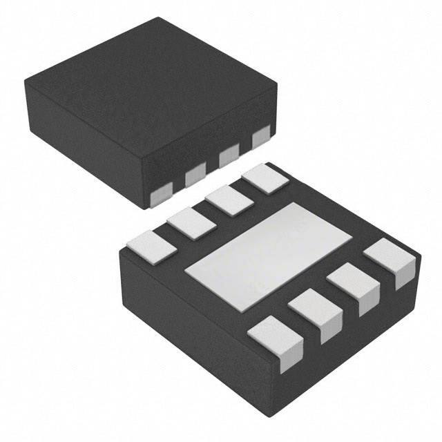
Device Information(1)
PART NUMBER
TL4242
PACKAGE
WSON (8)
BODY SIZE (NOM)
4.00 mm × 4.00 mm
(1) For all available packages, see the orderable addendum at
the end of the data sheet.
Simplified Schematic
Microcontroller
ST
Power
Supply or
Battery
PWM
Q
I
TL4242
REF
GND
D
1
An IMPORTANT NOTICE at the end of this data sheet addresses availability, warranty, changes, use in safety-critical applications,
intellectual property matters and other important disclaimers. PRODUCTION DATA.
�TL4242
SLVS641B – APRIL 2008 – REVISED MARCH 2015
www.ti.com
Table of Contents
1
2
3
4
5
6
7
Features ..................................................................
Applications ...........................................................
Description .............................................................
Revision History.....................................................
Pin Configuration and Functions .........................
Specifications.........................................................
1
1
1
2
3
3
6.1
6.2
6.3
6.4
6.5
6.6
3
4
4
4
4
6
Absolute Maximum Ratings ......................................
ESD Ratings..............................................................
Recommended Operating Conditions.......................
Thermal Information ..................................................
Electrical Characteristics...........................................
Typical Characteristics ..............................................
7.3 Feature Description................................................... 7
7.4 Device Functional Modes.......................................... 8
8
Application and Implementation .......................... 9
8.1 Application Information.............................................. 9
8.2 Typical Application .................................................. 10
9 Power Supply Recommendations...................... 12
10 Layout................................................................... 12
10.1 Layout Guidelines ................................................. 12
10.2 Layout Example .................................................... 12
11 Device and Documentation Support ................. 13
Detailed Description .............................................. 7
11.1 Trademarks ........................................................... 13
11.2 Electrostatic Discharge Caution ............................ 13
11.3 Glossary ................................................................ 13
7.1 Overview ................................................................... 7
7.2 Functional Block Diagram ......................................... 7
12 Mechanical, Packaging, and Orderable
Information ........................................................... 13
4 Revision History
Changes from Revision A (April 2011) to Revision B
•
2
Page
Added ESD Ratings table, Feature Description section, Device Functional Modes, Application and Implementation
section, Power Supply Recommendations section, Layout section, Device and Documentation Support section, and
Mechanical, Packaging, and Orderable Information section. ................................................................................................ 1
Submit Documentation Feedback
Copyright © 2008–2015, Texas Instruments Incorporated
Product Folder Links: TL4242
�TL4242
www.ti.com
SLVS641B – APRIL 2008 – REVISED MARCH 2015
5 Pin Configuration and Functions
DRJ Package
8-Pin WSON
(Top View)
PWM
1
8
GND
2 Exposed 7
Thermal
3
6
Pad
REF
4
ST
5
I
NC
Q
D
NC – No internal connection
Pin Functions
PIN
I/O
DESCRIPTION
NO.
NAME
1
PWM
I
Pulse-width modulation input. If not used, connect to I.
2
ST
O
Status output. Open-collector output. Connect to an external pullup resistor (RPULLUP ≥ 4.7 kΩ).
3
GND
—
Ground
4
REF
I
Reference input. Connect to a shunt resistor.
5
D
I
Status delay. To set status reaction delay, connect to GND with a capacitor. If no delay is needed, leave
open.
6
Q
O
Output
7
NC
—
No internal connection
8
I
I
—
Thermal
Pad
—
Input. Connect directly to GND as close as possible to the device with a 100-nF ceramic capacitor.
The thermal pad must be soldered directly to the PCB. It may be connected to ground or left floating.
6 Specifications
6.1 Absolute Maximum Ratings
over operating free-air temperature range (unless otherwise noted) (1)
VCC
VI
MIN
MAX
UNIT
–42
45
V
D
–0.3
7
PWM
–40
40
REF
–1
16
Q
–1
41
ST
–0.3
40
Supply voltage (2)
Input voltage
VO
Output voltage
IO
Output current
PWM
±1
REF
±2
ST
±5
V
V
mA
TJ
Virtual-junction temperature
–40
150
°C
Tstg
Storage temperature
–50
150
°C
(1)
(2)
Stresses beyond those listed under Absolute Maximum Ratings may cause permanent damage to the device. These are stress ratings
only, and functional operation of the device at these or any other conditions beyond those indicated under Recommended Operating
Conditions is not implied. Exposure to absolute-maximum-rated conditions for extended periods may affect device reliability.
All voltage values are with respect to the network ground terminal.
Submit Documentation Feedback
Copyright © 2008–2015, Texas Instruments Incorporated
Product Folder Links: TL4242
3
�TL4242
SLVS641B – APRIL 2008 – REVISED MARCH 2015
www.ti.com
6.2 ESD Ratings
VALUE
V(ESD)
(1)
(2)
Electrostatic discharge
Human-body model (HBM), per ANSI/ESDA/JEDEC JS-001 (1)
±1000
Charged-device model (CDM), per JEDEC specification JESD22C101 (2)
±1000
UNIT
V
JEDEC document JEP155 states that 500-V HBM allows safe manufacturing with a standard ESD control process.
JEDEC document JEP157 states that 250-V CDM allows safe manufacturing with a standard ESD control process.
6.3 Recommended Operating Conditions
MIN
MAX
UNIT
4.5
42
V
16
V
VCC
Supply voltage
VST
Status (ST) output voltage
VPWM
PWM voltage
0
40
V
CD
Status delay (D) capacitance
0
2.2
μF
RREF
Reference (REF) resistor
0
10
Ω
TJ
Virtual-junction temperature
–40
150
°C
6.4 Thermal Information
TL4242
THERMAL METRIC (1)
DRJ (WSON)
UNIT
8 PINS
RθJA
Junction-to-ambient thermal resistance
39.0
RθJC(top)
Junction-to-case (top) thermal resistance
31.5
RθJB
Junction-to-board thermal resistance
15.5
ψJT
Junction-to-top characterization parameter
0.3
ψJB
Junction-to-board characterization parameter
15.6
RθJC(bot)
Junction-to-case (bottom) thermal resistance
1.8
(1)
°C/W
For more information about traditional and new thermal metrics, see the IC Package Thermal Metrics application report, SPRA953.
6.5 Electrical Characteristics
over recommended operating free-air temperature range, VI = 13.5 V, RREF = 0.47 Ω, VPWM,H, TJ = –40°C to 150°C, all
voltages with respect to ground (unless otherwise noted)
TYP
MAX
IqL
Supply current
PARAMETER
VQ = 6.6 V
TEST CONDITIONS
MIN
12
22
UNIT
mA
IqOFF
Supply current, off mode
PWM = L, TJ < 85°C
0.1
2
μA
357
376
395
VQ – VREF = 6.6 V, RREF = 1 Ω
168
177
185
VQ – VREF = 6.6 V, RREF = 0.39 Ω
431
454
476
VQ – VREF = 5.4 V to 7.8 V, VI = 9
V to 16 V
357
376
395
OUTPUT ELECTRICAL CHARACTERISTICS
VQ – VREF
IQ
Output current
(1)
= 6.6 V
IQmax
Output current limit
RREF = 0 Ω
600
Vdr
Drop voltage
IQ = 300 mA
0.35
mA
mA
0.7
V
PWM INPUT ELECTRICAL CHARACTERISTICS
VPWM,
High-level PWM voltage
2.6
V
H
VPWM,
Low-level PWM voltage
0.7
V
500
μA
1
μA
L
IPWM,H High-level PWM input current
VPWM = 5 V
IPWM,L
VPWM = 0 V
(1)
4
Low-level PWM input current
220
–1
VQ – VREF equals the forward voltage sum of the connected LEDs (see Figure 3).
Submit Documentation Feedback
Copyright © 2008–2015, Texas Instruments Incorporated
Product Folder Links: TL4242
�TL4242
www.ti.com
SLVS641B – APRIL 2008 – REVISED MARCH 2015
Electrical Characteristics (continued)
over recommended operating free-air temperature range, VI = 13.5 V, RREF = 0.47 Ω, VPWM,H, TJ = –40°C to 150°C, all
voltages with respect to ground (unless otherwise noted)
PARAMETER
tPWM,O
TEST CONDITIONS
MIN
TYP
MAX
Delay time, turn on
70% of IQnom, See Figure 5
0
15
40
μs
Delay time, turn off
30% of IQnom, See Figure 5
0
15
40
μs
N
tPWM,O
FF
UNIT
REFERENCE (REF) ELECTRICAL CHARACTERISTICS
VREF
Reference voltage
RREF = 0.39 Ω to 1 Ω
168
177
185
mV
IREF
Reference input current
VREF = 180 mV
–1
0.1
1
μA
15
25
STATUS OUTPUT (ST) ELECTRICAL CHARACTERISTICS
VIQL
Lower status-switching threshold
ST = L
VIQH
Upper status-switching threshold
ST = H
VSTL
Low-level status voltage
IST = 1.5 mA
ISTLK
Leakage current
VST = 5 V
30
mV
40
mV
0.4
V
5
μA
10
14
ms
10
20
μs
STATUS DELAY (D) ELECTRICAL CHARACTERISTICS
tSTHL
Delay time, status reaction
CD = 47 nF, ST H→L
tSTLH
Delay time, status release
CD = 47 nF, ST L→H
6
Submit Documentation Feedback
Copyright © 2008–2015, Texas Instruments Incorporated
Product Folder Links: TL4242
5
�TL4242
SLVS641B – APRIL 2008 – REVISED MARCH 2015
www.ti.com
6.6 Typical Characteristics
450
700
400
600
IOUT – Output Current – mA
IOUT – Output Current – mA
350
500
400
300
200
300
250
200
150
100
50
100
0
-50
0
0
0.25
0.5
0.75
1
1.25
1.5
1.75
2
0
2.25
5
Figure 1. Output Current vs External Resistor
25
30
35
40
60
50
IPWM – PWM Current – µA
178.0
VREF – Reference Voltage – mV
20
Figure 2. Output Current vs Supply Voltage
178.5
177.5
177.0
176.5
176.0
40
30
20
10
0
-10
-20
0
20
40
60
80
100 120 140
0
Figure 3. Reference Voltage vs Junction Temperature
10
20
30
40
VPWM – PWM Voltage – V
TJ – Virtual Junction Temperature – °C
6
15
VCC – Supply Voltage – V
RREF – 8W
175.5
-40
10
Figure 4. PWM Pin Input Current vs PWM Voltage
Submit Documentation Feedback
Copyright © 2008–2015, Texas Instruments Incorporated
Product Folder Links: TL4242
�TL4242
www.ti.com
SLVS641B – APRIL 2008 – REVISED MARCH 2015
7 Detailed Description
7.1 Overview
The TL4242 device is an integrated, adjustable, constant-current source that can drive loads up to 500 mA. The
output current level can be adjusted through an external resistor. The device is designed to supply high-power
LEDs. Protection circuits prevent damage to the device in case of overload, short circuit, reverse polarity, and
overtemperature. The connected LEDs are protected against reverse polarity as well as excess voltages up to 45
V. The integrated PWM input of the TL4242 permits LED brightness regulation by pulse-width modulation
(PWM). Due to the high input impedance of the PWM input, the LED driver can be operated as a protected highside switch.
7.2 Functional Block Diagram
I
PWM
6
8
1
Q
Bias Supply
+
−
Bandgap
Reference
4
REF
Comparator
2
ST
Status
Delay
3
GND
5
D
7.3 Feature Description
7.3.1
PWM Input
The integrated PWM input of the TL4242 permits LED brightness regulation by pulse-width modulation (PWM).
The overall LED brightness is a function of the shunt resistor, RREF, and the PWM duty cycle. The PWM input
can also function as a simple enable control. When the PWM input is below VPWM,L, the device will go to a lowpower consumption sleep mode. Due to the high input impedance of the PWM input, the LED driver can be
operated as a protected high-side switch.
The LEDs are driven by a supply current that is adjusted by the resistor, RREF, preventing brightness variations
due to forward voltage spread of the LEDs. The luminosity spread arising from the LED production process can
be compensated through software by an appropriate duty cycle applied to the PWM pin. Therefore, it is not
necessary to select LEDs for forward voltage or luminosity classes.
7.3.2
ST Output
The status output of the LED driver (ST) detects an open-load condition, enabling supervision of correct LED
operation. An LED failure is detected as a voltage drop at the shunt resistor (RREF) below 25 mV (typical). In this
case, the status output pin (ST) is set low after a delay time adjustable by an optional capacitor connected to
pin D.
Submit Documentation Feedback
Copyright © 2008–2015, Texas Instruments Incorporated
Product Folder Links: TL4242
7
�TL4242
SLVS641B – APRIL 2008 – REVISED MARCH 2015
www.ti.com
Feature Description (continued)
7.3.2.1 Function and Timing Diagram
The functionality and timing of ST and PWM are shown in Figure 5. The status delay can be adjusted through
the capacitor connected to pin D. Delay time scales linearly with capacitance, CD:
CD
t STHL,typ +
10 ms
47 nF
(1)
CD
t STLH,typ +
10 ms
47 nF
(2)
Open
Load
VPWM
Open
Load
VPWM,H
VPWM,L
IQ
t
tPWM,ON
tPWM,OFF
IQ,nom
70%
30%
t
VD
tSTHL
VLD
t
VST
t
Figure 5. Function and Timing Diagram
7.4 Device Functional Modes
Table 1. Functional Modes
8
VPWM
DEVICE MODE
High
Active
Low
Sleep
Submit Documentation Feedback
Copyright © 2008–2015, Texas Instruments Incorporated
Product Folder Links: TL4242
�TL4242
www.ti.com
SLVS641B – APRIL 2008 – REVISED MARCH 2015
8 Application and Implementation
NOTE
Information in the following applications sections is not part of the TI component
specification, and TI does not warrant its accuracy or completeness. TI’s customers are
responsible for determining suitability of components for their purposes. Customers should
validate and test their design implementation to confirm system functionality.
8.1 Application Information
8.1.1
Input Supply Voltage
The input supply voltage calculates as the sum of the LED forward voltages, the TL4242 drop voltage, and the
voltage drop across the shunt resistor, RREF. The total LED forward voltage depends on the type of LED and the
number of LEDs in the string. The TL4242 drop voltage must be greater than Vdr (typically 350 mV), but must not
be too high as this could cause excessive power dissipation inside the device. The voltage drop across the shunt
resistor is typically 177 mV.
8.1.2 Power Dissipation in TL4242
Power dissipation in the TL4242 will come from two sources:
• Quiescent power: (Input voltage × Supply current)
• Power dissipation in the pass element:
((VI – VQ) × IQ)
(3)
The power dissipation in the pass element can be significant if the input voltage, VI, is much higher than VQ. The
power dissipation is also dependent on the LED current. Equation 4 is an example calculation using the design
parameters listed in Table 2.
Table 2. Design Parameters
DESIGN PARAMETER
EXAMPLE VALUE
VI
13.5 V
VQ
7V
IQ
0.2 A
((VI – VQ) × IQ) = (13.5 – 7) × 0.2 = 1.3 W
(4)
In Equation 4, there is 1.3 W of power dissipation in the pass element of the TL4242. This power dissipation will
cause the junction temperature of the device to increase. The increase in temperature is equal to RθJA × 1.3 W.
Please note that RθJA is dependent on the PCB layout.
8.1.3 Setting the Output Current
An external shunt resistor in the ground path of the connected LEDs is used to sense the LED current. A
regulation loop holds the voltage drop at the shunt resistor at a constant level of 177 mV (typical). The constantcurrent level can be adjusted by selecting the shunt resistance, RREF. Calculate the typical output current using
the equation:
IQ,typ = VREF/RREF
where
•
VREF is the reference voltage (typically 177 mV) (see Electrical Characteristics ).
(5)
The equation applies for RREF = 0.39 Ω to 10 Ω.
The output current is shown as a function of the reference resistance in Figure 1.
Submit Documentation Feedback
Copyright © 2008–2015, Texas Instruments Incorporated
Product Folder Links: TL4242
9
�TL4242
SLVS641B – APRIL 2008 – REVISED MARCH 2015
www.ti.com
8.2 Typical Application
Figure 6 shows a typical application with the TL4242 driving three LEDs in series.
VBAT
I
RO
SI
Microcontroller
Q
RADJ
GND
10 µF
D
10 kΩ
100 nF
PWM
ST
I
Q
TL4242
REF
GND
LED
Dragon
D
47 nF
0.47 Ω
0.25 W
RREF
Figure 6. Application Circuit
8.2.1 Design Requirements
For this design example, use the following as the input parameters in Table 3.
Table 3. Design Parameters
DESIGN PARAMETERS
EXAMPLE VALUE
# of LEDs
3
Forward Voltage of each LED
3.5 V
LED Current
377 mA
8.2.2 Detailed Design Procedure
8.2.2.1 Input Voltage
The input voltage must be greater than the sum of the LED forward voltages, the TL4242 drop voltage, and the
voltage drop across the shunt resistor, RREF. In this design example, the total LED forward voltage is 3 × 3.5 V =
10.5 V. The typical TL4242 drop voltage is 350 mV. The typical voltage drop across the shunt resistor is 177 mV.
In sum, the input voltage must be greater than 10.5 + 0.350 + 0.177 = 11.027 V. An appropriate input voltage for
this application would be 12 V.
8.2.2.2 Shunt Resistor
The shunt resistor value, RREF, can be calculated based on the desired LED current.
IQ,typ = VREF/RREF
where
•
VREF is the reference voltage (typically 177 mV) (see Electrical Characteristics).
(6)
As shown in Design Requirements, the desired LED current is 377 mA. The appropriate RREF value for this
application calculates to be 0.47 Ω.
10
Submit Documentation Feedback
Copyright © 2008–2015, Texas Instruments Incorporated
Product Folder Links: TL4242
�TL4242
www.ti.com
SLVS641B – APRIL 2008 – REVISED MARCH 2015
8.2.3 Application Curve
700
IOUT – Output Current – mA
600
500
400
300
200
100
0
0
0.25
0.5
0.75
1
1.25
1.5
1.75
2
2.25
RREF – 8W
Figure 7. Output Current vs External Resistor
Submit Documentation Feedback
Copyright © 2008–2015, Texas Instruments Incorporated
Product Folder Links: TL4242
11
�TL4242
SLVS641B – APRIL 2008 – REVISED MARCH 2015
www.ti.com
9 Power Supply Recommendations
The input voltage at the I pin must be greater than the sum of the LED forward voltages, the voltage drop across
the TL4242 (from I to Q), and the voltage drop across the shunt resistor RREF. For an example of this calculation,
refer to Typical Application. The input voltage should not exceed the recommended maximum operation voltage
of 42 V.
10 Layout
10.1 Layout Guidelines
The REF pin should be routed directly to the shunt resistor, RREF. If there is a long PCB trace between the LED
string and the shunt resistor, the REF pin should connect close to the shunt resistor (rather than close to the LED
string) to allow for accurate sensing across the shunt resistor.
The traces for I and Q will carry the full LED current. These traces should be the appropriate width to carry the
LED current.
The exposed thermal pad on the bottom of the TL4242 should be connected to the PCB. The thermal pad helps
to dissipate heat in the case of high power dissipation in the device. To further enhance the thermal performance
of the device, the thermal pad can be connected by vias to the ground layer in the PCB.
10.2 Layout Example
To µC
PWM
To µC
ST
I
NC
GND
Q
REF
D
To pullup
source
To power supply
RREF
Via to GND Plane
Figure 8. PCB Layout
12
Submit Documentation Feedback
Copyright © 2008–2015, Texas Instruments Incorporated
Product Folder Links: TL4242
�TL4242
www.ti.com
SLVS641B – APRIL 2008 – REVISED MARCH 2015
11 Device and Documentation Support
11.1 Trademarks
All trademarks are the property of their respective owners.
11.2 Electrostatic Discharge Caution
These devices have limited built-in ESD protection. The leads should be shorted together or the device placed in conductive foam
during storage or handling to prevent electrostatic damage to the MOS gates.
11.3 Glossary
SLYZ022 — TI Glossary.
This glossary lists and explains terms, acronyms, and definitions.
12 Mechanical, Packaging, and Orderable Information
The following pages include mechanical, packaging, and orderable information. This information is the most
current data available for the designated devices. This data is subject to change without notice and revision of
this document. For browser-based versions of this data sheet, refer to the left-hand navigation.
Submit Documentation Feedback
Copyright © 2008–2015, Texas Instruments Incorporated
Product Folder Links: TL4242
13
�PACKAGE OPTION ADDENDUM
www.ti.com
6-Feb-2020
PACKAGING INFORMATION
Orderable Device
Status
(1)
TL4242DRJR
Package Type Package Pins Package
Drawing
Qty
ACTIVE
SON
DRJ
8
3000
Eco Plan
Lead/Ball Finish
MSL Peak Temp
(2)
(6)
(3)
Green (RoHS
& no Sb/Br)
NIPDAU
Level-3-260C-168 HR
Op Temp (°C)
Device Marking
(4/5)
-40 to 125
T4242
(1)
The marketing status values are defined as follows:
ACTIVE: Product device recommended for new designs.
LIFEBUY: TI has announced that the device will be discontinued, and a lifetime-buy period is in effect.
NRND: Not recommended for new designs. Device is in production to support existing customers, but TI does not recommend using this part in a new design.
PREVIEW: Device has been announced but is not in production. Samples may or may not be available.
OBSOLETE: TI has discontinued the production of the device.
(2)
RoHS: TI defines "RoHS" to mean semiconductor products that are compliant with the current EU RoHS requirements for all 10 RoHS substances, including the requirement that RoHS substance
do not exceed 0.1% by weight in homogeneous materials. Where designed to be soldered at high temperatures, "RoHS" products are suitable for use in specified lead-free processes. TI may
reference these types of products as "Pb-Free".
RoHS Exempt: TI defines "RoHS Exempt" to mean products that contain lead but are compliant with EU RoHS pursuant to a specific EU RoHS exemption.
Green: TI defines "Green" to mean the content of Chlorine (Cl) and Bromine (Br) based flame retardants meet JS709B low halogen requirements of


 工商网监
湘ICP备2023018690号
工商网监
湘ICP备2023018690号

