TLC59282
SBVS152C – DECEMBER 2010 – REVISED OCTOBER 2011
www.ti.com
16-Channel, Constant-Current LED Driver with 4-Channel Grouped Delay
Check for Samples: TLC59282
FEATURES
APPLICATIONS
•
•
•
•
1
2
•
•
•
•
•
•
•
•
•
•
16 Channels, Constant-Current Sink Output
with On/Off Control
Capability (Constant-Current Sink):
35 mA (VCC ≤ 3.6 V), 45 mA (VCC > 3.6 V)
LED Power-Supply Voltage up to 17 V
VCC = 3 V to 5.5 V
Constant-Current Accuracy:
– Channel-to-Channel = ±0.6% (typ),
±2% (max)
– Device-to-Device = ±1% (typ), ±3% (max)
Low Saturation Voltage: 0.31 V at 20 mA (typ)
– TA = +25℃, One Channel On
CMOS Logic Level I/O
Data Transfer Rate: 35 MHz
BLANK Pulse Width: 30 ns
Four-Channel Grouped Delay for
Noise Reduction
Operating Temperature: –40°C to +85°C
VLED
Controller
The TLC59282 is a 16-channel, constant-current sink
driver. Each channel can be individually controlled via
a simple serial communications protocol that is
compatible with 3.3 V or 5 V CMOS logic levels,
depending on the operating VCC. Once the serial
data buffer is loaded, a rising edge on LATCH
transfers the data to the LEDx outputs. The BLANK
pin can be used to turn off all OUTn outputs during
power-on and output data latching to prevent
unwanted image displays during these times. The
constant-current value of all 16 channels is set by a
single external resistor. Multiple TLC59282s can be
cascaded together to control additional LEDs from the
same processor.
¼
¼
¼
¼
¼
OUT0
OUT15
SOUT
OUT15
SOUT
VCC
SCLK
LAT
VCC
VCC
BLANK
BLANK
IREF
¼
SIN
VCC
LAT
BLANK
VLED
¼
SCLK
LAT
VLED
¼
SIN
SCLK
DESCRIPTION
VLED
OUT0
DATA
Video Displays
Message Boards
Illumination
TLC59282
IC1
RIREF
IREF
GND
TLC59282
ICn
GND
RIREF
3
Typical Application Circuit (Multiple Daisy-Chained TLC59282s)
1
2
Please be aware that an important notice concerning availability, standard warranty, and use in critical applications of Texas
Instruments semiconductor products and disclaimers thereto appears at the end of this data sheet.
All trademarks are the property of their respective owners.
PRODUCTION DATA information is current as of publication date.
Products conform to specifications per the terms of the Texas
Instruments standard warranty. Production processing does not
necessarily include testing of all parameters.
Copyright © 2010–2011, Texas Instruments Incorporated
�TLC59282
SBVS152C – DECEMBER 2010 – REVISED OCTOBER 2011
www.ti.com
This integrated circuit can be damaged by ESD. Texas Instruments recommends that all integrated circuits be handled with
appropriate precautions. Failure to observe proper handling and installation procedures can cause damage.
ESD damage can range from subtle performance degradation to complete device failure. Precision integrated circuits may be more
susceptible to damage because very small parametric changes could cause the device not to meet its published specifications.
PACKAGE/ORDERING INFORMATION (1)
PRODUCT
(1)
PACKAGE-LEAD
TLC59282
SSOP-24/QSOP-24
TLC59282
QFN-24
ORDERING NUMBER
TRANSPORT MEDIA, QUANTITY
TLC59282DBQR
Tape and Reel, 2500
TLC59282DBQ
Tube, 50
TLC59282RGER
Tape and Reel, 3000
TLC59282RGE
Tape and Reel, 250
For the most current package and ordering information, see the Package Option Addendum at the end of this document, or visit the
device product folder at www.ti.com.
ABSOLUTE MAXIMUM RATINGS (1) (2)
Over operating free-air temperature range, unless otherwise noted.
PARAMETER
TLC59282
UNIT
–0.3 to +6
V
50
mA
–0.3 to VCC + 0.3
V
VCC
Supply voltage
IOUT
Output current (dc)
OUT0 to OUT15
VIN
Input voltage range
SIN, SCLK, LAT, BLANK, IREF
SOUT
–0.3 to VCC + 0.3
V
VOUT
Output voltage range
TJ(MAX)
Operating junction temperature
TSTG
Storage temperature range
ESD rating
(1)
(2)
–0.3 to +18
V
+150
°C
–55 to +150
°C
Human body model (HBM)
4000
V
Charged device model (CDM)
1000
V
OUT0 to OUT15
Stresses above these ratings may cause permanent damage. Exposure to absolute maximum conditions for extended periods may
degrade device reliability. These are stress ratings only, and functional operation of the device at these or any other conditions beyond
those specified is not supported.
All voltage values are with respect to network ground terminal.
THERMAL INFORMATION
TLC59282
THERMAL METRIC (1)
DBQ
RGE
24 PINS
24 PINS
θJA
Junction-to-ambient thermal resistance
73.2
46.8
θJCtop
Junction-to-case (top) thermal resistance
44.6
48.6
θJB
Junction-to-board thermal resistance
38.9
23.0
ψJT
Junction-to-top characterization parameter
12.3
1.2
ψJB
Junction-to-board characterization parameter
39.7
22.9
θJCbot
Junction-to-case (bottom) thermal resistance
n/a
6.3
(1)
2
UNITS
°C/W
For more information about traditional and new thermal metrics, see the IC Package Thermal Metrics application report, SPRA953.
Submit Documentation Feedback
Copyright © 2010–2011, Texas Instruments Incorporated
Product Folder Link(s): TLC59282
�TLC59282
SBVS152C – DECEMBER 2010 – REVISED OCTOBER 2011
www.ti.com
RECOMMENDED OPERATING CONDITIONS
At TA= –40°C to +85°C, unless otherwise noted.
TLC59282
PARAMETER
TEST CONDITIONS
MIN
NOM
MAX
UNIT
DC Characteristics: VCC = 3 V to 5.5 V
VCC
Supply voltage
VO
Voltage applied to output
VIH
High-level input voltage
VIL
Low-level input voltage
IOH
High-level output current
IOL
Low-level output current
IOLC
3
5.5
V
17
V
0.7 × VCC
VCC
V
GND
0.3 × VCC
OUT0 to OUT15
Constant output sink current
V
SOUT
–1
mA
SOUT
1
mA
OUT0 to OUT15,
3 V ≤ VCC < 3.6 V
2
35
mA
OUT0 to OUT15,
3.6 V ≤ VCC < 5.5 V
2
45
mA
TA
Operating free-air temperature range
–40
+85
°C
TJ
Operating junction temperature range
–40
+125
°C
AC Characteristics: VCC = 3 V to 5.5 V
fCLK
(SCLK)
Data shift clock frequency
TWH0
SCLK
35
MHz
SCLK
10
ns
SCLK
10
ns
LAT
20
ns
TWH2
BLANK
60
ns
TWL2
BLANK
30
ns
TWL0
TWH1
TSU0
TSU1
TH0
TH1
Pulse duration
Setup time
Hold time
SIN–SCLK↑
4
ns
LAT↓–SCLK↑
10
ns
SIN–SCLK↑
4
ns
LAT↓–SCLK↑
10
ns
Submit Documentation Feedback
Copyright © 2010–2011, Texas Instruments Incorporated
Product Folder Link(s): TLC59282
3
�TLC59282
SBVS152C – DECEMBER 2010 – REVISED OCTOBER 2011
www.ti.com
ELECTRICAL CHARACTERISTICS
At VCC = 3 V to 5.5 V and TA = –40°C to +85°C. Typical values at VCC = 3.3 V and TA = +25°C, unless otherwise noted.
TLC59282
PARAMETER
TEST CONDITIONS
VOH
High-level output voltage
IOH = –1 mA at SOUT
VOL
Low-level output voltage
IOL = 1 mA at SOUT
IIN
Input current
VIN = VCC or GND at SIN and SCLK
MIN
TYP
VCC – 0.4
MAX
UNIT
VCC
V
–1
0.4
V
1
μA
ICC0
SIN/SCLK/LAT = low, BLANK = high, VOUTn = 1 V,
RIREF = open
0.1
1
mA
ICC1
SIN/SCLK/LAT = low, BLANK = high, VOUTn = 1 V,
RIREF = 3 kΩ (IOUT = 16.8 mA target)
4.5
6
mA
7
15
mA
16
34
mA
33.7
35.3
mA
0.1
μA
Supply current (VCC)
ICC2
All OUTn = ON, SIN/SCLK/LAT/BLANK = low,
VOUTn = 1 V, RIREF = 3 kΩ
ICC3
All OUTn = ON, SIN/SCLK/LAT/BLANK = low,
VOUTn = 1 V, RIREF = 1.5 kΩ (IOUT = 33.6mA target)
IOLC
Constant output current
All OUTn = ON, VOUTn = VOUTfix = 1 V, RIREF = 1.5 kΩ
at OUT0 to OUT15 (see Figure 6), TA = +25°C
IOLKG
Output leakage current
OUTn = OFF, VOUTn = VOUTfix = 17 V, BLANK = high,
RIREF = 1.5 kΩ at OUT0 to OUT15 (see Figure 6)
ΔIOLC0
Constant-current error
(channel-to-channel) (1)
All OUTn = ON, VOUTn = VOUTfix = 1 V, RIREF = 1.5 kΩ
at OUT0 to OUT15
±0.6
±2
%
ΔIOLC1
Constant-current error
(device-to-device) (2)
All OUTn = ON, VOUTn = VOUTfix = 1 V, RIREF = 1.5 kΩ
at OUT0 to OUT15, TA = +25°C
±1
±3
%
ΔIOLC2
Line regulation (3)
All OUTn = ON, VOUTn = VOUTfix = 1 V, RIREF = 1.5 kΩ
at OUT0 to OUT15, VCC = 3 V to 5.5 V
±0.5
±1
%/V
ΔIOLC3
Load regulation (4)
All OUTn = ON, VOUTn = 1 V to 3V, VOUTfix = 1 V,
RIREF = 1.5 kΩ
±1
±3
%/V
VIREF
Reference voltage output
RIREF = 1.5 kΩ, TA = +25°C
1.18
1.205
1.23
V
RPUP
Pull-up resistor
BLANK
250
500
750
kΩ
RPDWN
Pull-down resistor
LAT
250
500
750
kΩ
(1)
32.1
The deviation of each output from the average of OUT0–OUT15 constant-current. Deviation is calculated by the formula:
IOUTn
D (%) =
-1
´ 100
(IOUT0 + IOUT1 + ... + IOUT14 + IOUT15)
(2)
16
.
The deviation of the OUT0–OUT15 constant-current average from the ideal constant-current value.
Deviation is calculated by the following formula:
(IOUT0 + IOUT1 + ... IOUT14 + IOUT15)
- (Ideal Output Current)
16
D (%) =
´ 100
Ideal Output Current
Ideal current is calculated by the formula:
IOUT(IDEAL) = 41.9 ´
(3)
1.205
RIREF
Line regulation is calculated by this equation:
D (%/V) =
(IOUTn at VCC = 5.5 V) - (IOUTn at VCC = 3 V)
(4)
5.5 V - 3 V
Load regulation is calculated by the equation:
D (%/V) =
(IOUTn at VOUTn = 3 V) - (IOUTn at VOUTn = 1 V)
100
´
(IOUTn at VOUTn = 1 V)
4
100
´
(IOUTn at VCC = 3 V)
3V-1V
Submit Documentation Feedback
Copyright © 2010–2011, Texas Instruments Incorporated
Product Folder Link(s): TLC59282
�TLC59282
SBVS152C – DECEMBER 2010 – REVISED OCTOBER 2011
www.ti.com
SWITCHING CHARACTERISTICS
At VCC = 3 V to 5.5 V, TA = –40°C to +85°C, CL = 15 pF, RL = 130 Ω, RIREF = 1.5 kΩ, and VLED = 5.5 V. Typical values at VCC
= 3.3 V and TA = +25°C, unless otherwise noted.
TLC59282
PARAMETER
tR0
Rise time
tR1
tF0
Fall time
tF1
TEST CONDITIONS
MIN
TYP
MAX
UNIT
SOUT (see Figure 5)
5
12
ns
OUTn (see Figure 4)
10
30
ns
SOUT (see Figure 5)
5
12
ns
OUTn (see Figure 4)
10
30
ns
tD0
SCLK↑ to SOUT↑↓
8
20
ns
tD1
LAT↑ or BLANK↑↓ to OUT0/OUT7/OUT8/OUT15 on/off
18
36
ns
tD2
LAT↑ or BLANK↑↓ to OUT1/OUT6/OUT9/OUT14 on/off
38
69
ns
tD3
LAT↑ or BLANK↑↓ to OUT2/OUT5/OUT10/OUT13
on/off
58
102
ns
tD4
LAT↑ or BLANK↑↓ to OUT3/OUT4/OUT11/OUT12
on/off
78
135
ns
15
ns
Propagation delay time
tON_ERR
(1)
Output on-time error (1)
On/off latch data = all '1', 30 ns BLANK low level
one-shot pulse input
–15
Output on-time error (tON_ERR) is calculated by the formula: tON_ERR (ns) = tOUT_ON – BLANK low level one-shot pulse width (TWL2).
tOUT_ON indicates the actual on-time of the constant-current output.
FUNCTIONAL BLOCK DIAGRAM
VCC
VCC
SIN
LSB
MSB
16-Bit Shift Register
(1 Bit x 16 Channels)
SCLK
0
SOUT
15
¼
MSB
LSB
LAT
Output On/Off Data Latch
(1 Bit x 16 Channels)
0
15
¼
BLANK
16-Channel Constant-Current Sink Driver
with 4-Channel Grouped Delay
IREF
GND
GND
¼
OUT0
OUT1
OUT14 OUT15
Submit Documentation Feedback
Copyright © 2010–2011, Texas Instruments Incorporated
Product Folder Link(s): TLC59282
5
�TLC59282
SBVS152C – DECEMBER 2010 – REVISED OCTOBER 2011
www.ti.com
DEVICE INFORMATION
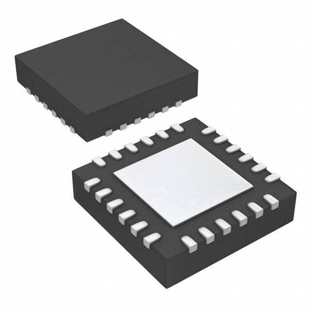
SSOP-24/QSOP-24
DBQ PACKAGE
(TOP VIEW)
SCLK
SIN
GND
VCC
IREF
SOUT
24
23
22
21
20
19
QFN-24
RGE PACKAGE
(TOP VIEW)
GND
1
24
VCC
SIN
2
23
IREF
SCLK
3
22
SOUT
LAT
4
21
BLANK
LAT
1
18
BLANK
OUT0
5
20
OUT15
OUT0
2
17
OUT15
OUT1
6
19
OUT14
OUT1
3
16
OUT14
OUT2
7
18
OUT13
OUT2
4
15
OUT13
OUT3
8
17
OUT12
OUT3
5
14
OUT12
OUT4
9
16
OUT11
OUT4
6
13
OUT11
OUT5
10
15
OUT10
OUT6
11
14
OUT9
OUT7
12
13
OUT8
7
8
9
10
11
12
OUT5
OUT6
OUT7
OUT8
OUT9
OUT10
Thermal Pad
(Bottom Side)
NOTE: Thermal pad is not connected to GND internally. The
thermal pad must be connected to GND via the PCB pattern.
6
Submit Documentation Feedback
Copyright © 2010–2011, Texas Instruments Incorporated
Product Folder Link(s): TLC59282
�TLC59282
SBVS152C – DECEMBER 2010 – REVISED OCTOBER 2011
www.ti.com
TERMINAL FUNCTIONS
TERMINAL
NAME
DBQ
RGE
I/O
DESCRIPTION
SIN
2
23
I
Serial data input for driver on/off control; Schmitt buffer input. When SIN is high, data '1' are
written into the LSB of the 16-bit shift register at the SCLK rising edge.
SCLK
3
24
I
Serial data shift clock; Schmitt buffer input. All data in the 16-bit shift register are shifted toward
the MSB by 1-bit synchronization of SCLK.
I
Level triggered latch; Schmitt buffer input. The data in the 16-bit shift register continue to transfer
to the output on/off data latch while LAT is high. Therefore, if the data in the 16-bit shift register
are changed when LAT is high, the data in the data latch are also changed. The data in the data
latch are held when LAT is low. This pin is internally pulled down to GND with a 500 kΩ (typ)
resistor.
Blank, all outputs; Schmitt buffer input. When BLANK is high, all constant-current outputs
(OUT0–OUT15) are forced off. When BLANK is low, all constant-current outputs are controlled by
the data in the output on/off data latch. This pin is internally pulled up to VCC with a 500 kΩ (typ)
resistor.
LAT
4
1
BLANK
21
18
I
IREF
23
20
I/O
Constant-current value setting, OUT0–OUT15 sink constant-current is set to desired value by
connection to an external resistor between IREF and GND.
SOUT
22
19
O
Serial data output. This output is connected to the MSB of the 16-bit shift register. SOUT data
changes at the rising edge of SCLK.
OUT0
5
2
O
Constant-current output. Each output can be tied together with others to increase the
constant-current. Different voltages can be applied to each output.
OUT1
6
3
O
Constant-current output
OUT2
7
4
O
Constant-current output
OUT3
8
5
O
Constant-current output
OUT4
9
6
O
Constant-current output
OUT5
10
7
O
Constant-current output
OUT6
11
8
O
Constant-current output
OUT7
12
9
O
Constant-current output
OUT8
13
10
O
Constant-current output
OUT9
14
11
O
Constant-current output
OUT10
15
12
O
Constant-current output
OUT11
16
13
O
Constant-current output
OUT12
17
14
O
Constant-current output
OUT13
18
15
O
Constant-current output
OUT14
19
16
O
Constant-current output
OUT15
20
17
O
Constant-current output
VCC
24
21
—
Power-supply voltage
GND
1
22
—
Power ground
Submit Documentation Feedback
Copyright © 2010–2011, Texas Instruments Incorporated
Product Folder Link(s): TLC59282
7
�TLC59282
SBVS152C – DECEMBER 2010 – REVISED OCTOBER 2011
www.ti.com
PARAMETER MEASUREMENT INFORMATION
PIN EQUIVALENT INPUT AND OUTPUT SCHEMATIC DIAGRAMS
VCC
VCC
INPUT
OUTPUT
GND
GND
Figure 1. SIN, SCLK, LAT, BLANK
Figure 2. SOUT
OUTn
GND
Figure 3. OUT0 Through OUT15
TEST CIRCUITS
RL
VCC
VCC
VCC
OUTn
IREF
RIREF
CL
GND
VLED
(1)
SOUT
VCC
GND
CL
(1)
(1) CL includes measurement probe and jig capacitance.
Figure 4. Rise Time and Fall Time Test Circuit for
OUTn
VCC
Figure 5. Rise Time and Fall Time Test Circuit for
SOUT
OUT0
¼
VCC
(1) CL includes measurement probe and jig capacitance.
IREF
¼
RIREF
OUTn
GND OUT15
VOUTfix
VOUTn
Figure 6. Constant-Current Test Circuit for OUTn
8
Submit Documentation Feedback
Copyright © 2010–2011, Texas Instruments Incorporated
Product Folder Link(s): TLC59282
�TLC59282
SBVS152C – DECEMBER 2010 – REVISED OCTOBER 2011
www.ti.com
TIMING DIAGRAMS
TWH0, TWL0, TWH1, TWH2, TWL2:
VCC
(1)
INPUT
50%
GND
TWH
TWL
TSU0, TSU1, TH0, TH1:
VCC
CLOCK
(1)
INPUT
50%
GND
TSU
TH
VCC
DATA/CONTROL
(1)
INPUT
50%
GND
(1)
Input pulse rise and fall time is 1 ns to 3 ns.
Figure 7. Input Timing
tR0, tR1, tF0, tF1, tD0, tD1, tD2, tD3, tD4:
VCC
(1)
INPUT
50%
GND
tD
VOH or VOUTn
90%
OUTPUT
50%
10%
VOL or VOUTn
tR or tF
(1)
Input pulse rise and fall time is 1 ns to 3 ns.
Figure 8. Output Timing
Submit Documentation Feedback
Copyright © 2010–2011, Texas Instruments Incorporated
Product Folder Link(s): TLC59282
9
�TLC59282
SBVS152C – DECEMBER 2010 – REVISED OCTOBER 2011
SIN
DATA
0A
DATA
15B
DATA
13B
DATA
14B
DATA
12B
www.ti.com
DATA
11B
DATA
3B
DATA
2B
DATA
1B
DATA
0B
TH0
TSU0
TH1
TWH0
DATA
15C
DATA
14C
DATA
13C
DATA
12C
DATA
11C
DATA
10C
1
2
3
TWL0
4
5
6
TSU1
SCLK
1
2
3
4
5
13
14
15
16
TWH1
LAT
DATA
0A
DATA
15B
DATA
14B
DATA
13B
DATA
12B
DATA
3B
DATA
2B
DATA
1B
DATA
0B
DATA
15C
DATA
14C
DATA
13C
DATA
12C
DATA
11C
Shift Register
LSB+1 Data (Internal)
DATA
1A
DATA
0A
DATA
15B
DATA
14B
DATA
13B
DATA
4B
DATA
3B
DATA
2B
DATA
1B
DATA
0B
DATA
15C
DATA
14C
DATA
13C
DATA
12C
Shift Register
MSB-1 Data (Internal)
DATA
14A
DATA
13A
DATA
12A
DATA
11A
DATA
10A
DATA
2A
DATA
1A
DATA
15B
DATA
14B
DATA
13B
DATA
12B
DATA
11B
DATA
10B
DATA
9B
Shift Register
MSB Data (Internal)
DATA
15A
DATA
14A
DATA
13A
DATA
12A
DATA
11A
DATA
3A
DATA
2A
DATA
1A
DATA
15B
DATA
14B
DATA
13B
DATA
12B
DATA
11B
DATA
10B
¼
¼
Output On/Off Control
Data Latch (Internal)
SOUT
¼
Shift Register
LSB Data (Internal)
Previous On/Off Control Data
DATA
15A
DATA
14A
DATA
13A
DATA
12A
tD0
DATA
2A
DATA
1A
DATA
0A
Latest On/Off Control Data
DATA
15B
DATA
14B
DATA
13B
DATA
12B
DATA
11B
DATA
10B
tWH2
tR0/tF0
BLANK
tWL2
OUT0/7/8/15
(1)
OFF
tD1
tD1
OFF
ON
ON
tOUTON
OUT1/6/9/14
(1)
OFF
tD2
tD2
ON
tD3
OUT2/5/10/13
OUT3/4/11/12
(1)
OFF
OFF
tD3
OFF
ON
ON
(1)
OFF
ON
tF1
tD4
ON
tD4
OFF
ON
tR1
(1) Output on/off data = FFFFh.
(2) tON_ERR = tOUTON – TWL2.
Figure 9. Timing Diagram
10
Submit Documentation Feedback
Copyright © 2010–2011, Texas Instruments Incorporated
Product Folder Link(s): TLC59282
�TLC59282
SBVS152C – DECEMBER 2010 – REVISED OCTOBER 2011
www.ti.com
TYPICAL CHARACTERISTICS
At VCC = 3.3 V and TA = +25°C, unless otherwise noted.
REFERENCE RESISTOR
vs OUTPUT CURRENT
OUTPUT CURRENT vs
OUTPUT VOLTAGE
100 k
50
TA = +25°C
Output Current (mA)
Reference Resistor (W)
45
25245
10098
10 k
5049
3366
2524
2020
1k
0
20
10
IO = 35 mA
35
IO = 30 mA
30
25
IO = 20 mA
20
15
IO = 10 mA
10
1683 1443
1262
IO = 2 mA
0
40
30
0
50
2
3
2.5
Output Voltage (V)
Figure 11.
OUTPUT CURRENT vs
OUTPUT VOLTAGE
ΔIOLC vs AMBIENT TEMPERATURE
4
IO = 35 mA
IO = 35 mA
3
38
2
37
DIOLC (%)
Output Current (mA)
1.5
1
0.5
Figure 10.
39
IO = 5 mA
5
1122 1010
Output Current (mA)
40
IO = 40 mA
IO = 45 mA
40
36
35
34
33
TA = -40°C
32
TA = +25°C
31
TA = +85°C
1
0
-1
-2
VCC = 3.3 V
-3
VCC = 5 V
-4
30
0
1.5
1
0.5
2
2.5
3
-40
-20
0
20
40
60
80
100
Ambient Temperature (°C)
Output Voltage (V)
Figure 12.
Figure 13.
ΔIOLC vs OUTPUT CURRENT
CONSTANT-CURRENT OUTPUT
VOLTAGE WAVEFORM
4
TA = +25°C
CH1-BLANK
(30 ns)
CH1 (2 V/div)
3
DIOLC (%)
2
1
CH2-OUT0
(BLANK = 30 ns)
CH2 (2 V/div)
0
-1
CH3 (2 V/div)
-2
VCC = 3.3 V
-3
VCC = 5 V
-4
0
10
20
30
40
50
IOLC = 35 mA, TA = +25°C
RL = 130 W, CL = 15 pF
VCC = 3.3 V, VLED = 5.5 V
CH3-OUT3
(BLANK = 30 ns)
Time (20 ns/div)
Output Current (mA)
Figure 14.
Figure 15.
Submit Documentation Feedback
Copyright © 2010–2011, Texas Instruments Incorporated
Product Folder Link(s): TLC59282
11
�TLC59282
SBVS152C – DECEMBER 2010 – REVISED OCTOBER 2011
www.ti.com
DETAILED DESCRIPTION
SETTING FOR THE CONSTANT SINK CURRENT VALUE
The constant-current values are determined by an external resistor (RIREF) placed between IREF and GND. The
resistor (RIREF) value is calculated by Equation 1.
RIREF (kW) =
VIREF (V)
´ 41.9
IOLC (mA)
Where:
VIREF = the internal reference voltage on the IREF pin (typically 1.205 V)
(1)
IOLC must be set in the range of 2 mA to 35 mA when VCC is less than 3.6 V. Also, when VCC is equal to 3.6 V or
greater, IOLC must be set in the range of 2 mA to 45 mA. The constant sink current characteristic for the external
resistor value is shown in Figure 10. Table 1 describes the constant-current output versus external resistor value.
Table 1. Constant-Current Output versus External Resistor Value
IOLC (mA, Typical)
RIREF (kΩ)
45 (VCC > 3.6 V only)
1.12
40 (VCC > 3.6 V only)
1.26
35
1.44
30
1.68
25
2.02
20
2.52
15
3.37
10
5.05
5
10.1
2
25.2
CONSTANT-CURRENT DRIVER ON/OFF CONTROL
When BLANK is low, the corresponding output is turned on if the data in the on/off control data latch are '1' and
remains off if the data are '0'. When BLANK is high, all outputs are forced off. This control is shown in Table 2.
Table 2. On/Off Control Data Truth Table
OUTPUT ON/OFF DATA
CONSTANT-CURRENT OUTPUT
STATUS
0
Off
1
On
When the IC is initially powered on, the data in the 16-bit shift register and output on/off data latch are not set to
the respective default value. Therefore, the output on/off data must be written to the data latch before turning the
constant-current output on. BLANK should be at a high level when powered on because the constant-current
may be turned on as a result of random data in the output on/off data latch.
The output on/off data corresponding to any unconnected OUTn outputs should be set to '0' before turning on the
remaining outputs. Otherwise, the supply current (ICC) increases while the LEDs are on.
12
Submit Documentation Feedback
Copyright © 2010–2011, Texas Instruments Incorporated
Product Folder Link(s): TLC59282
�TLC59282
SBVS152C – DECEMBER 2010 – REVISED OCTOBER 2011
www.ti.com
REGISTER CONFIGURATION
The TLC59282 has a 16-bit shift register and an output on/off data latch. Both the shift register and data latch
are 16 bits long and are used to turn the constant-current outputs on and off. Figure 16 shows the shift register
and data latch configuration. The data at the SIN pin are shifted in to the LSB of the 16-bit shift register at the
rising edge of the SCLK pin; SOUT data change at the rising edge of SCLK.
The output on/off data in the 16-bit shift register continue to transfer to the output on/off data latch while LAT is
high. Therefore, if the data in the 16-bit shift register are changed when LAT is high, the data in the data latch
are also changed. The data in the data latch are held when LAT is low. When the IC initially powers on, the data
in the output on/off shift register and latch are not set to the default values; on/off control data must be written to
the on/off control data latch before turning the constant-current output on. BLANK should be high when the IC is
powered on because the constant-current may be turned on at that time as a result of random values in the
on/off data latch. All constant-current outputs are forced off when BLANK is high. The OUTn on/off are controlled
by the data in the output on/off data latch. The timing diagram and truth table for writing data are shown in
Figure 17 and Table 3.
16-Bit Shift Register (1 Bit ´ 16 Channels)
SOUT
MSB
15
14
13
12
On/Off Data
for
OUT15
On/Off Data
for
OUT14
On/Off Data
for
OUT13
On/Off Data
for
OUT12
4
11
¼
3
2
1
LSB
0
On/Off Data
for
OUT3
On/Off Data
for
OUT2
On/Off Data
for
OUT1
On/Off Data
for
OUT0
3
2
1
LSB
0
On/Off Data
for
OUT3
On/Off Data
for
OUT2
On/Off Data
for
OUT1
On/Off Data
for
OUT0
SIN
SCLK
¼
MSB
15
14
13
12
On/Off Data
for
OUT15
On/Off Data
for
OUT14
On/Off Data
for
OUT13
On/Off Data
for
OUT12
Output On/Off Data Latch (1 Bit ´ 16 Channels)
4
11
¼
LAT
16 Bits
To Constant-Current Driver Control Block
Figure 16. 16-Bit Shift Register and Output On/Off Data Latch Configuration
Submit Documentation Feedback
Copyright © 2010–2011, Texas Instruments Incorporated
Product Folder Link(s): TLC59282
13
�TLC59282
SBVS152C – DECEMBER 2010 – REVISED OCTOBER 2011
0
1
2
3
4
5
D15
D14
D13
D12
D11 D10
www.ti.com
6
7
8
9
10
11
12
13
14
15
SCLK
D9
D8
D7
D6
D5
D4
D3
D2
D1
D0
SIN
LAT
BLANK
D0
OFF
OUT0
ON
OUT1
D1
OUT2
D2
D3
OUT3
OFF
ON
OFF
ON
OFF
ON
SOUT
¼
¼
¼
¼
D15
OUT15
OFF
ON
D15
Don’t Care
Figure 17. Operation Timing Diagram
Table 3. Truth Table in Operation
SCLK
LAT
BLANK
SIN
OUT0…OUT7…OUT15
SOUT
↑
High
Low
Dn
Dn…Dn – 7…Dn – 15
Dn – 15
↑
Low
Low
Dn + 1
No change
Dn – 14
↑
High
Low
Dn + 2
Dn + 2…Dn – 5…Dn – 13
Dn – 13
↓
—
Low
Dn + 3
Dn + 2…Dn – 5…Dn – 13
Dn – 13
↓
—
High
Dn + 3
Off
Dn – 13
NOISE REDUCTION
Large surge currents may flow through the IC and the board if all 16 outputs turn on or off simultaneously. These
large current surges could induce detrimental noise and electromagnetic interference (EMI) into other circuits.
The TLC59282 independently turns on or off the outputs for each color group with a 20 ns (typ) delay time; see
Figure 9. The output current sinks are grouped into four groups. The first group that is turned on/off are
OUT0/7/8/15; the second group that is turned on/off are OUT1/6/9/14; the third group that is turned on/off are
OUT2/5/10/13; and the fourth group is OUT3/4/11/12. Both turn-on and turn-off are delayed. However, the state
of each output is controlled by the data in the output on-off data latch and BLANK level.
14
Submit Documentation Feedback
Copyright © 2010–2011, Texas Instruments Incorporated
Product Folder Link(s): TLC59282
�TLC59282
SBVS152C – DECEMBER 2010 – REVISED OCTOBER 2011
www.ti.com
REVISION HISTORY
NOTE: Page numbers for previous revisions may differ from page numbers in the current version.
Changes from Revision B (July 2011) to Revision C
•
Page
Added Low Saturation Voltage Features bullet .................................................................................................................... 1
Changes from Revision A (December 2010) to Revision B
Page
•
Changed Constant-Current Accuracy Features bullet .......................................................................................................... 1
•
Added RGE package information to Package/Ordering Information table ........................................................................... 2
•
Added RGE package to Thermal Information table .............................................................................................................. 2
•
Changed Input current parameter test conditions in Electrical Characteristics table ........................................................... 4
•
Added RGE pin out and footnote to Device Information section .......................................................................................... 6
•
Added RGE information to Terminal Functions table ........................................................................................................... 7
•
Deleted Figure 11, POWER DISSIPATION RATE vs FREE-AIR TEMPERATURE .......................................................... 11
Submit Documentation Feedback
Copyright © 2010–2011, Texas Instruments Incorporated
Product Folder Link(s): TLC59282
15
�PACKAGE OPTION ADDENDUM
www.ti.com
10-Dec-2020
PACKAGING INFORMATION
Orderable Device
Status
(1)
Package Type Package Pins Package
Drawing
Qty
Eco Plan
(2)
Lead finish/
Ball material
MSL Peak Temp
Op Temp (°C)
Device Marking
(3)
(4/5)
(6)
TLC59282DBQ
ACTIVE
SSOP
DBQ
24
50
RoHS & Green
NIPDAU
Level-2-260C-1 YEAR
-40 to 85
TLC59282
TLC59282DBQR
ACTIVE
SSOP
DBQ
24
2500
RoHS & Green
NIPDAU
Level-2-260C-1 YEAR
-40 to 85
TLC59282
TLC59282RGER
ACTIVE
VQFN
RGE
24
3000
RoHS & Green
NIPDAU
Level-2-260C-1 YEAR
-40 to 85
TLC
59282
TLC59282RGET
ACTIVE
VQFN
RGE
24
250
RoHS & Green
NIPDAU
Level-2-260C-1 YEAR
-40 to 85
TLC
59282
(1)
The marketing status values are defined as follows:
ACTIVE: Product device recommended for new designs.
LIFEBUY: TI has announced that the device will be discontinued, and a lifetime-buy period is in effect.
NRND: Not recommended for new designs. Device is in production to support existing customers, but TI does not recommend using this part in a new design.
PREVIEW: Device has been announced but is not in production. Samples may or may not be available.
OBSOLETE: TI has discontinued the production of the device.
(2)
RoHS: TI defines "RoHS" to mean semiconductor products that are compliant with the current EU RoHS requirements for all 10 RoHS substances, including the requirement that RoHS substance
do not exceed 0.1% by weight in homogeneous materials. Where designed to be soldered at high temperatures, "RoHS" products are suitable for use in specified lead-free processes. TI may
reference these types of products as "Pb-Free".
RoHS Exempt: TI defines "RoHS Exempt" to mean products that contain lead but are compliant with EU RoHS pursuant to a specific EU RoHS exemption.
Green: TI defines "Green" to mean the content of Chlorine (Cl) and Bromine (Br) based flame retardants meet JS709B low halogen requirements of


 工商网监
湘ICP备2023018690号
工商网监
湘ICP备2023018690号
