Sample &
Buy
Product
Folder
Support &
Community
Tools &
Software
Technical
Documents
TLC5954
SBVS241 – APRIL 2014
TLC5954 48-Channel, Constant-Current LED Driver with Global Brightness Control,
LED Open-Short Detection, and Power-Save Mode
1 Features
2 Applications
•
•
•
•
1
•
•
•
•
•
•
•
•
•
•
•
•
•
•
•
48 Constant-Current Sink Output Channels with
On or Off Control
Current Capability:
– 34.9 mA for 32 Channels
– 24.4 mA 16 Channels
No External Resistor for Current Setting
Maximum Current Control (MC): 3 Bits (8 Steps)
Global Brightness Control (BC) for Each Color
Group: 7 Bits (128 Steps), Three Groups
LED Power-Supply Voltage: Up to 10 V
VCC = 3.0 V to 3.6 V
Constant-Current Accuracy:
– Channel-to-Channel = ±1% (typ), ±3% (max)
– Device-to-Device = ±2% (typ), ±4% (max)
Data Transfer Rate: 30 MHz
BLANK Pulse Duration: 40 ns (min)
LED Open Detection (LOD)
LED Short Detection (LSD)
Power-Save Mode (PSM): 7-µA Consumption,
High-Speed Recovery
Undervoltage Lockout Sets Default Data
Delayed Switching Minimizes Inrush Current
Operating Temperature: –40°C to +85°C
LED Video Displays
Variable Message Signs (VMS)
Illumination
3 Description
The TLC5954 is a 48-channel, constant-current sink
LED driver. Each channel can be turned on or off by
writing data to an internal register. The output
channels (OUTXn) are grouped into three groups of
16 channels. Each channel group (R, G, and B) has a
128-step global brightness control (BC) function. The
maximum current value of all 48 channels can be set
with an 8-step maximum current control (MC)
function. The device has two error flags: LED open
detection (LOD) and LED short detection (LSD). The
error flags can be read via a serial interface port. The
device also has a power-save mode that sets the
total current consumption to 7 µA (typ) when all
outputs are off.
Device Information(1)
DEVICE NAME
TLC5954
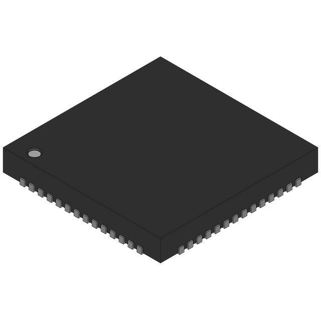
PACKAGE
VQFN (56)
BODY SIZE
8 mm × 8 mm
(1) For all available packages, see the orderable addendum at
the end of the datasheet.
space
space
space
space
Application Circuit
VLED
+
GND
Input Serial Data
x48
OUTR0
SIN
Shift Clock
SCLK
Data Latch
LAT
BLANK Signal
OUTB15
Output Serial Data
SOUT
VCC
TLC5954
VCC
BLANK
GND
GND
PowerPAD
GND
1
An IMPORTANT NOTICE at the end of this data sheet addresses availability, warranty, changes, use in safety-critical applications,
intellectual property matters and other important disclaimers. PRODUCTION DATA.
�TLC5954
SBVS241 – APRIL 2014
www.ti.com
Table of Contents
1
2
3
4
5
6
7
Features ..................................................................
Applications ...........................................................
Description .............................................................
Revision History.....................................................
Pin Configuration and Functions .........................
Specifications.........................................................
1
1
1
2
3
4
6.1
6.2
6.3
6.4
6.5
6.6
6.7
4
5
5
6
6
7
8
Absolute Maximum Ratings ......................................
Handling Ratings.......................................................
Recommended Operating Conditions.......................
Thermal Information ..................................................
Electrical Characteristics...........................................
Switching Characteristics ..........................................
Typical Characteristics ..............................................
8.1
8.2
8.3
8.4
8.5
9
16
17
18
23
27
Applications and Implementation ...................... 33
9.1 Application Information............................................ 33
9.2 Typical Application .................................................. 33
10 Power Supply Recommendations ..................... 36
11 Layout................................................................... 36
11.1 Layout Guidelines ................................................. 36
11.2 Layout Example .................................................... 37
12 Device and Documentation Support ................. 38
12.1
12.2
12.3
12.4
12.5
Parameter Measurement Information ................ 11
7.1
Pin Equivalent Input and Output Schematic
Diagrams.................................................................. 11
7.2 Test Circuits ............................................................ 11
7.3 Timing Diagrams ..................................................... 12
8
Overview .................................................................
Functional Block Diagram .......................................
Feature Description ................................................
Device Functional Modes........................................
Register Maps .........................................................
Device Support......................................................
Documentation Support ........................................
Trademarks ...........................................................
Electrostatic Discharge Caution ............................
Glossary ................................................................
38
38
38
38
38
13 Mechanical, Packaging, and Orderable
Information ........................................................... 38
Detailed Description ............................................ 16
4 Revision History
2
Date
Revision
Notes
April 2014
*
Initial release.
Submit Documentation Feedback
Copyright © 2014, Texas Instruments Incorporated
Product Folder Links: TLC5954
�TLC5954
www.ti.com
SBVS241 – APRIL 2014
5 Pin Configuration and Functions
GND
OUTR13
OUTB12
OUTG12
OUTR12
OUTB11
OUTG11
OUTR11
OUTB10
OUTG10
OUTR10
55
54
53
52
51
50
49
48
47
46
45
44
VCC
OUTG13
56
1
OUTB13
GND
RTQ Package
VQFN-56
(Top View)
43
42
SOUT
OUTR14
2
41
OUTB9
OUTG14
3
40
OUTG9
OUTB14
4
39
OUTR9
OUTR15
5
38
OUTB8
OUTG15
6
37
OUTG8
OUTB15
7
36
OUTR8
OUTR0
8
35
OUTB7
OUTG0
9
34
OUTG7
OUTB0
10
33
OUTR7
OUTR1
11
32
OUTB6
OUTG1
12
31
OUTG6
OUTB1
13
30
OUTR6
OUTR2
14
29
BLANK
15
16
17
18
19
20
21
22
23
24
25
26
27
28
OUTG2
OUTB2
OUTR3
OUTG3
OUTB3
OUTR4
OUTG4
OUTB4
OUTR5
OUTG5
OUTB5
SIN
LAT
SCLK
Thermal P ad
(Solder Side, GND Terminal)
Submit Documentation Feedback
Copyright © 2014, Texas Instruments Incorporated
Product Folder Links: TLC5954
3
�TLC5954
SBVS241 – APRIL 2014
www.ti.com
Pin Functions
PIN
NAME
NO.
I/O
DESCRIPTION
GND
1, 56
—
Ground. All GND pins are connected internally.
OUTR0 to
OUTR15
2, 5, 8, 11, 14, 17, 20,
23, 30, 33, 36, 39, 44,
47, 50, 53
O
Red LED constant-current outputs (OUTRn).
Multiple outputs can be tied together to increase the constant-current capability. Different voltages can be
applied to each output. These outputs are turned on or off by the BLANK signal and the data in the output on
or off control data latch.
OUTG0 to
OUTG15
3, 6, 9, 12, 15, 18, 21,
24, 31, 34, 37, 40, 45,
48, 51, 54
O
Green LED constant-current outputs (OUTGn).
Multiple outputs can be tied together to increase the constant-current capability. Different voltages can be
applied to each output. These outputs are turned on or off by the BLANK signal and the data in the output on
or off control data latch.
OUTB0 to
OUTB15
4, 7, 10, 13, 16, 19, 22,
25, 32, 35, 38, 41, 46,
49, 52, 55
O
Blue LED constant-current outputs (OUTBn).
Multiple outputs can be tied together to increase the constant-current capability. Different voltages can be
applied to each output. These outputs are turned on or off by the BLANK signal and the data in the output on
or off control data latch.
26
I
Serial data input of the 49-bit common shift register, Schmitt buffer input.
When SIN is high, the LSB is set to 1 for only one SCLK input rising edge. If two SCLK rising edges are input
while SIN is high, then the 49-bit shift register LSB and LSB+1 are set to 1. When SIN is low, the LSB is set to
0 at the SCLK input rising edge.
SIN
LAT
27
I
Edge-triggered latch, Schmitt buffer input.
The LAT rising edge latches data from the common shift register either into the output on or off data latch or
the maximum current control (MC), brightness control (BC), or function control (FC) data latch. When the
common shift register data are latched into the on or off data latch, data in the common shift register are
simultaneously replaced with SID, which is selected by SIDLD. Refer to the Output On or Off Data Latch and
Status Information Data (SID) sections for more details.
SCLK
28
I
Serial data shift clock, Schmitt buffer input.
Data present on SIN are shifted to the 49-bit common shift register LSB with the SCLK rising edge. Data in the
shift register are shifted towards the MSB at each SCLK rising edge. The common shift register MSB appears
on SOUT.
BLANK
29
I
Blank all outputs, Schmitt buffer input.
When BLANK is high, all constant-current outputs (OUTXn) are forced off. When BLANK is low, all OUTXn are
controlled by the on or off control data in the data latch.
SOUT
42
O
Serial data output of the 49-bit common shift register.
SOUT is connected to the MSB of the register. Data are clocked out at the SCLK rising edge.
43
—
Power-supply voltage
—
Ground. The thermal pad must be connected to GND on the printed circuit board (PCB).
VCC
Thermal pad
6 Specifications
6.1 Absolute Maximum Ratings
over operating free-air temperature range (unless otherwise noted) (1)
MIN
(2)
VCC
Supply voltage
VIN
Input voltage range
VOUT
Output voltage range
TJ (max)
Operating junction temperature
(1)
(2)
4
MAX
UNIT
–0.3
4.0
V
SIN, SCLK, LAT, BLANK
–0.3
VCC + 0.3
V
SOUT
–0.3
VCC + 0.3
V
OUTR0 to OUTR15, OUTG0 to OUTG15,
OUTB0 to OUTB15
–0.3
11
V
150
°C
Stresses beyond those listed under Absolute Maximum Ratings may cause permanent damage to the device. These are stress ratings
only, and functional operation of the device at these or any other conditions beyond those indicated under Recommended Operating
Conditions is not implied. Exposure to absolute-maximum-rated conditions for extended periods my affect device reliability.
All voltages are with respect to device ground pin.
Submit Documentation Feedback
Copyright © 2014, Texas Instruments Incorporated
Product Folder Links: TLC5954
�TLC5954
www.ti.com
SBVS241 – APRIL 2014
6.2 Handling Ratings
Tstg
V(ESD)
(1)
(2)
MIN
MAX
UNIT
–55
150
°C
Human body model (HBM), per ANSI/ESDA/JEDEC JS-001, all
pins (1)
–200
2000
V
Charged device model (CDM), per JEDEC specification
JESD22-C101, all pins (2)
–500
500
V
Storage temperature range
Electrostatic discharge
JEDEC document JEP155 states that 500-V HBM allows safe manufacturing with a standard ESD control process.
JEDEC document JEP157 states that 250-V CDM allows safe manufacturing with a standard ESD control process.
6.3 Recommended Operating Conditions
At TA= –40°C to +85°C, unless otherwise noted.
PARAMETER
TEST CONDITIONS
MIN
NOM
MAX
UNIT
DC CHARACTERISTICS (VCC = 3 V to 3.6 V)
VCC
Supply voltage
3.0
3.6
V
10
V
V
VO
Voltage applied to output
OUTR0 to OUTR15, OUTG0 to
OUTG15, OUTB0 to OUTB15
VIH
High-level input voltage
SIN, SCLK, LAT, BLANK
0.7 × VCC
VCC
VIL
Low-level input voltage
SIN, SCLK, LAT, BLANK
GND
0.3 × VCC
IOH
High-level output current
SOUT
–2
mA
IOL
Low-level output current
SOUT
2
mA
TA
Operating free-air temperature
range
–40
+85
°C
TJ
Operating junction temperature
range
–40
+125
°C
V
AC CHARACTERISTICS (VCC = 3 V to 3.6 V)
fCLK (SCLK)
Data shift clock frequency
tWH0
SCLK
30
MHz
SCLK
10
ns
SCLK
10
ns
LAT
15
ns
tWH2
BLANK
60
ns
tWL2
BLANK
40
ns
tSU0
SIN to SCLK↑
4
ns
tSU1
LAT↓ to SCLK↑
20
ns
tSU2
SCLK↑ resumes normal mode,
BLANK↓, PSMODE bit = 01b
12
µs
LAT↑ for all data latching except all
0s resumes normal mode, BLANK↓,
PSMODE bit = 10b
12
µs
3
ns
10
ns
tWL0
tWH1
Pulse duration
Setup time
tSU3
tH0
tH1
Hold time
SCLK↑ to SIN
SCLK↑ to LAT↑
Submit Documentation Feedback
Copyright © 2014, Texas Instruments Incorporated
Product Folder Links: TLC5954
5
�TLC5954
SBVS241 – APRIL 2014
www.ti.com
6.4 Thermal Information
TLC5954
THERMAL METRIC (1)
RTQ (VQFN)
UNIT
56 PINS
RθJA
Junction-to-ambient thermal resistance
29.1
RθJCtop
Junction-to-case (top) thermal resistance
16.3
RθJB
Junction-to-board thermal resistance
7.7
ψJT
Junction-to-top characterization parameter
0.3
ψJB
Junction-to-board characterization parameter
7.7
RθJCbot
Junction-to-case (bottom) thermal resistance
2.8
(1)
°C/W
For more information about traditional and new thermal metrics, see the IC Package Thermal Metrics application report, SPRA953.
6.5 Electrical Characteristics
At TA = –40°C to +85°C and VCC = 3.0 V to 3.6 V, unless otherwise noted. Typical values are at TA = +25°C and VCC = 3.3 V.
PARAMETER
TEST CONDITIONS
VOH
High-level output voltage
IOH = –2 mA at SOUT
VOL
Low-level output voltage
IOL = 2 mA at SOUT
MIN
TYP
VCC – 0.4
MAX
UNIT
VCC
V
0.4
V
VLOD0
LODVLT = 000b
0.15
0.20
0.25
V
VLOD1
LODVLT = 001b, 101b, 110b, 111b
0.25
0.30
0.35
V
LODVLT = 010b
0.35
0.40
0.45
V
VLOD3
LODVLT = 011b
0.45
0.50
0.55
V
VLOD4
LODVLT = 100b
0.55
0.60
0.65
V
VLSD0
LSDVLT = 00b
0.45 × VCC
0.50 × VCC
0.55 × VCC
V
LSDVLT = 01b
0.65 × VCC
0.70 × VCC
0.75 × VCC
V
LSDVLT = 10b, 11b
0.85 × VCC
0.90 × VCC
0.95 × VCC
V
1
μA
VLOD2
LED open-detection threshold
VLSD1
LED short-detection threshold
VLSD2
IIN
Input current
VIN = VCC or GND at SIN, SCLK, LAT, and BLANK
–1
ICC0
SIN, SCLK, LAT = GND, BLANK = VCC, VOUTXn = 1 V,
BCX = 7Fh, MC = 0h (IOUTRn, IOUTGn = 2.9-mA target,
IOUTBn = 2.0-mA target) (1)
15
19
mA
ICC1
SIN, SCLK, LAT = GND, BLANK = VCC, VOUTXn = 1 V,
BCX = 7Fh, MC = 5h (IOUTRn, IOUTGn = 17.4-mA target,
IOUTBn = 12.2-mA target)
17.5
22
mA
SIN, SCLK, LAT, BLANK = GND, all OUTXn = on,
VOUTXn = 1 V, BCX = 7Fh, MC = 5h
17.5
22
mA
ICC3
SIN, SCLK, LAT, BLANK = GND, all OUTXn = on,
VOUTXn = 1 V, BCX = 7Fh, MC = 7h (IOUTRn, IOUTGn =
34.9-mA target, IOUTBn = 24.4-mA target)
20.5
25.5
mA
ICC4
In power-save mode, SIN, SCLK, LAT = GND,
BLANK = VCC
7
60
µA
IOLC0
All OUTXn = on, VOUTXn = VOUTfix = 1 V, BC = 7Fh,
MC = 7h, at OUTR0 to OUTR15 and OUTG0 to
OUTG15
32.5
34.9
37.3
mA
IOLC1
All OUTXn = on, VOUTXn = VOUTfix = 1 V, BC = 7Fh,
MC = 7h, at OUTB0 to OUTB15
22.7
24.4
26.1
mA
TJ = +25°C
0.1
µA
IOLKG
BLANK = VCC, VOUTXn = VOUTfix
= 10 V, MC = 7h, at OUTXn
TJ = +85°C
0.2
µA
TJ = +125°C
0.5
µA
Supply current (VCC)
ICC2
Constant output current
Output leakage current
Constant-current error
(channel-to-channel) (2)
ΔIOLC0
(1)
(2)
All OUTXn = on, BCX = 7Fh, VOUTXn = VOUTfix = 1 V,
MC = 7h, at same color group (OUTXn)
±1%
±3%
X = R, G, and B. n = 0 to 15.
The deviation of each output in the same color group (OUTRn, OUTGn, OUTBn) from the average of the same OUTXn group constantcurrent. Deviation is calculated by the formula:
IOUTXn
D (%) =
IOUTX0 + IOUTX1 + ... + IOUTX14 + IOUTX15
-1
´ 100
16
, where X = R, G, or B, and n = 0 to 15.
6
Submit Documentation Feedback
Copyright © 2014, Texas Instruments Incorporated
Product Folder Links: TLC5954
�TLC5954
www.ti.com
SBVS241 – APRIL 2014
Electrical Characteristics (continued)
At TA = –40°C to +85°C and VCC = 3.0 V to 3.6 V, unless otherwise noted. Typical values are at TA = +25°C and VCC = 3.3 V.
TYP
MAX
ΔIOLC1
Constant-current error
(device-to-device) (3)
PARAMETER
All OUTXn = on, BCX = 7Fh, VOUTXn = VOUTfix = 1 V,
MC = 7h, at same color group (OUTXn)
±0.5%
±3%
ΔIOLC2
Line regulation (4)
All OUTXn = on, BCX = 7Fh, VOUTXn = VOUTfix = 1 V,
MC = 7h, at OUTXn
±0.5
±1
%/V
ΔIOLC3
Load regulation (5)
All OUTXn = on, BCX = 7Fh, VOUTXn = 1 V to 3 V,
VOUTfix = 1 V, MC = 7h, at OUTXn
±1
±3
%/V
(3)
TEST CONDITIONS
16
D (%) =
- (Ideal Output Current)
´ 100
Ideal Output Current
Ideal current is 34.9 mA for OUTRn and OUTGn. Ideal current is 24.4 mA for OUTBn with MC data equal to 7h.
, where X = R, G, or B, and n = 0 to 15.
Line regulation is calculated by the formula:
D (%/V) =
(5)
UNIT
The deviation of the OUTXn constant-current average from the ideal constant-current value. Deviation is calculated by the formula:
IOUTX0 + IOUTX1 + ... + IOUTX15
(4)
MIN
(IOUTXn at VCC = 3.6 V) - (IOUTXn at VCC = 3.0 V)
IOUTXn at VCC = 3.0 V
´
100
3.6 V - 3.0 V
X = R, G, or B. n = 0 to 15.
Load regulation is calculated by the equation:
D (%/V) =
(IOUTXn at VOUTXn = 3 V) - (IOUTXn at VOUTXn = 1 V)
IOUTXn at VOUTXn = 1 V
´
100
3V-1V
, where X = R, G, or B, and n = 0 to 15.
6.6 Switching Characteristics
At TA = –40°C to +85°C, VCC = 3.0 V to 3.6 V, CL = 15 pF, RL = 100 Ω for OUTRn and OUTGn, RL = 150 Ω for OUTBn,
MC = 7h, and VLED = 4.5 V, unless otherwise noted. Typical values at TA = +25°C and VCC = 3.3 V.
PARAMETER
TYP
MAX
2
5
ns
20
50
ns
2
5
ns
OUTXn, BCX = 7Fh
20
50
ns
tD0
SCLK↑ to SOUT
13
23
ns
tD1
LAT↑ to OUTR0 on to off or OUTR0 off to on, BCX = 7Fh
30
60
ns
tD2
BLANK↓↑ to OUTR0 on to off or OUTR0 off to on, BCX = 7Fh
30
60
ns
OUTRn on to OUTGn on, OUTGn on to OUTBn on, and OUTBn on to
the next OUTRn on, BCX = 7Fh
1.5
5
ns
OUTRn off to OUTGn off, OUTGn off to OUTBn off, and OUTBn off to
the next OUTRn off, BCX = 7Fh
1.5
5
ns
LAT↑ to power-save mode by writing data for all OUTXn off
150
300
ns
35
ns
tR0
TEST CONDITIONS
Rise time
tR1
tF0
OUTXn, BCX = 7Fh
Propagation delay (2)
tD3
tD4
tD5
tON_ERR
(1)
(2)
(3)
Output on-time error
(1)
SOUT
Fall time
tF1
MIN
SOUT
(3)
OUTXn on or off data = all 1s, BCX = 7Fh, 40-ns BLANK low-level oneshot pulse input
–35
UNIT
X = R, G, or B. n = 0 to 15.
tD3 (OUTRn on to OUTGn on, OUTGn on to OUTBn on, and OUTBn on to the next OUTRn on) and tD4 (OUTRn off to OUTGn off,
OUTGn off to OUTBn off, and OUTBn off to the next OUTRn off) are calculated by:
tD3 (ns) = (the propagation delay between OUTR0 on to OUTB7 on) / 47 and
tD4 (ns) = (the propagation delay between OUTR0 off to OUTB7 off) / 47.
Output on-time error (tON_ERR) is calculated by the formula: tON_ERR (ns) = tOUT_ON – BLANK low-level pulse duration.
tOUT_ON is the actual on-time of OUTXn.
Submit Documentation Feedback
Copyright © 2014, Texas Instruments Incorporated
Product Folder Links: TLC5954
7
�TLC5954
SBVS241 – APRIL 2014
www.ti.com
6.7 Typical Characteristics
At TA = +25°C and VCC = 3.3 V, unless otherwise noted.
45
35
MC = 0
MC = 1
40
MC = 2
MC = 3
MC = 4
MC = 5
MC = 6
MC = 7
MC = 1
MC = 2
30
MC = 3
MC = 4
MC = 5
MC = 6
MC = 7
MC = 8
Output Current (mA)
Output Current (mA)
35
30
25
20
15
25
20
15
10
10
5
5
0
0
0
0.5
1
1.5
2
Output Voltage (V)
2.5
3
0
BCR, BCG = 7Fh
1.5
2
Output Voltage (V)
2.5
38
27
37
26
36
35
34
TA = 25qC
TA = �40qC
TA = 85qC
33
D002
25
24
23
TA = 25qC
TA = �40qC
TA = 85qC
22
21
32
0
0.1
0.2
0.3
BCR = BCG = 7Fh
0.4 0.5 0.6 0.7
Output Voltage (V)
0.8
0.9
0
1
0.1
0.2
0.3
D003
MC = 7
BCB = 7Fh
Figure 3. Output Current vs Output Voltage
(OUTRn, OUTGn)
2
2
Constant-Current Error (%)
3
1
0
-1
0.4 0.5 0.6 0.7
Output Voltage (V)
0.8
0.9
1
D004
MC = 7
Figure 4. Output Current vs Output Voltage
(OUTBn)
3
-2
1
0
-1
-2
Min
Max
Min
Max
-3
-3
0
BCR = 7Fh
10
20
Output Current (mA)
30
40
0
D005
MC = 7
BCG = 7Fh
Figure 5. Constant-Current Error vs Output Current
(Channel-to-Channel, OUTRn)
8
3
Figure 2. Output Current vs Output Voltage
(OUTBn)
Output Current (mA)
Output Current (mA)
1
BCB = 7Fh
Figure 1. Output Current vs Output Voltage
(OUTRn, OUTGn)
Constant-Current Error (%)
0.5
D001
10
20
Output Current (mA)
30
40
D006
MC = 7
Figure 6. Constant-Current Error vs Output Current
(Channel-to-Channel, OUTGn)
Submit Documentation Feedback
Copyright © 2014, Texas Instruments Incorporated
Product Folder Links: TLC5954
�TLC5954
www.ti.com
SBVS241 – APRIL 2014
Typical Characteristics (continued)
3
3
2
2
Constant-Current Error (%)
Constant-Current Error (%)
At TA = +25°C and VCC = 3.3 V, unless otherwise noted.
1
0
-1
1
0
-1
-2
-2
Min
Max
Min
Max
-3
-40
-3
0
5
10
15
20
Output Current (mA)
BCB = 7Fh
25
30
MC = 7
0
20
40
60
Ambient Temperature (qC)
BCR = 7Fh
Figure 7. Constant-Current Error vs Output Current
(Channel-to-Channel, OUTBn)
3
3
2
2
1
0
-1
80
-2
D008
MC = 7h
1
0
-1
-2
Min
Max
-3
-40
-20
0
20
40
60
Ambient Temperature (qC)
BCG = 7Fh
80
Min
Max
-3
-40
100
-20
0
20
40
60
Ambient Temperature (qC)
D009
MC = 7h
BCB = 7Fh
Figure 9. Constant-Current Error vs Ambient Temperature
(Channel-to-Channel, OUTGn)
80
100
D010
MC = 7
Figure 10. Constant-Current Error vs Ambient Temperature
(Channel-to-Channel, OUTBn)
40
40
MC = 0
MC = 1
MC = 2
MC = 3
35
30
MC = 4
MC = 5
MC = 6
MC = 7
MC = 0
MC = 1
MC = 2
MC = 3
35
Output Current (mA)
Output Current (mA)
100
Figure 8. Constant-Current Error vs Ambient Temperature
(Channel-to-Channel, OUTRn)
Constant-Current Error (%)
Constant-Current Error (%)
-20
D007
25
20
15
10
5
30
MC = 4
MC = 5
MC = 6
MC = 7
25
20
15
10
5
0
0
0
16
32
48
64
80
96
Brightness Control Data (dec)
112
128
0
16
D011
BCR = BCG = 7Fh
32
48
64
80
96
Brightness Control Data (dec)
112
128
D012
BCB = 7Fh
Figure 11. Global Brightness Control Linearity
(OUTRn, OUTGn)
Figure 12. Global Brightness Control Linearity
(OUTBn)
Submit Documentation Feedback
Copyright © 2014, Texas Instruments Incorporated
Product Folder Links: TLC5954
9
�TLC5954
SBVS241 – APRIL 2014
www.ti.com
Typical Characteristics (continued)
25
25
20
20
Supply Current (mA)
Supply Current (mA)
At TA = +25°C and VCC = 3.3 V, unless otherwise noted.
15
10
15
10
5
5
0
0
5
SIN = 15 MHz
MC = 0h to 7h
SOUT = No Load
10
15
20
25
30
Red, Green Output Current (mA)
SCLK = 30 MHz
All OUTXn = On
VOUT = 0.8 V
35
40
0
-40
-20
0
D013
BCX = 7Fh
BLANK = Low
Figure 13. Supply Current vs Output Current
SIN = 15 MHz
All OUTXn = On
SOUT = No Load
TA = –40°C to +85°C
20
40
Temperature (qC)
BCX = 7Fh
SCLK = 30 MHz
60
80
100
D014
MC = 5h
BLANK = Low
VOUT = 0.8 V
Figure 14. Supply Current vs Ambient Temperature
Ch1: BLANK (2V/div)
Ch2: OUTR0 (2V/div)
Ch3: OUTG0 (2V/div)
Ch4: OUTB0 (2V/div)
VCC = 3.3 V
MC = 7h
BCX = 7Fh
RL = 100 Ω (OUTRn, OUTGn)
CL = 15 pF
BLANK Low Pulse Duration = 40 ns
VLED = 4.5 V
RL = 150 Ω (OUTBn)
Figure 15. Constant-Current Output Voltage Waveform
10
Submit Documentation Feedback
Copyright © 2014, Texas Instruments Incorporated
Product Folder Links: TLC5954
�TLC5954
www.ti.com
SBVS241 – APRIL 2014
7 Parameter Measurement Information
7.1
Pin Equivalent Input and Output Schematic Diagrams
VCC
VCC
OUTPUT
INPUT
GND
GND
Figure 16. SIN, SCLK, LAT, BLANK
Figure 17. SOUT
OUTR0
¼
VCC
VCC
OUTXn
(1)
¼
GND
OUTB15
VOUTfix
VOUTXn(1)
(1) X = R, G, or B. n = 0 to 15.
Figure 18. OUTXn
7.2 Test Circuits
VCC
RL
VCC
OUTXn
(2)
(1)
VCC
VCC
VLED
SOUT
CL
GND
GND
CL
(1)
(1) CL includes measurement probe and jig capacitance.
(1) CL includes measurement probe and jig capacitance.
(2) X = R, G, or B. n = 0 to 15.
Figure 20. Rise and Fall Time Test Circuit for
SOUT
Figure 19. Rise and Fall Time Test Circuit for
OUTXn
VCC
OUTR0
¼
VCC
OUTXn
(1)
¼
GND
OUTB15
VOUTfix
VOUTXn(1)
(1) X = R, G, or B. n = 0 to 15.
Figure 21. Constant-Current Test Circuit for OUTXn
Submit Documentation Feedback
Copyright © 2014, Texas Instruments Incorporated
Product Folder Links: TLC5954
11
�TLC5954
SBVS241 – APRIL 2014
www.ti.com
7.3 Timing Diagrams
tWH0, tWL0, tWH1, tWH2, tWL2
VCC
Input
(1)
50%
GND
tWH
tWL
tSU0, tSU1, tH0, tH1
VCC
Clock Input
(1)
50%
GND
tSU
tH
VCC
Data and Control Input
(1)
50%
GND
(1) Input pulse rise and fall time is 1 ns to 3 ns.
Figure 22. Input Timing
tR0, tR1, tF0, tF1, tD0, tD1, tD2, tD3, tD4, tD5:
VCC
Input
(1)
50%
GND
tD5
tD
VOH or VOUTXnH
90%
Output
(2)
50%
10%
VOL or VOUTXnL
tR or tF
(1) Input pulse rise and fall time is 1 ns to 3 ns.
(2) X = R, G, or B. n = 0 to 15.
Figure 23. Output Timing
12
Submit Documentation Feedback
Copyright © 2014, Texas Instruments Incorporated
Product Folder Links: TLC5954
�TLC5954
www.ti.com
SBVS241 – APRIL 2014
Timing Diagrams (continued)
Output on or off data write.
SIN
ON
R0A
FC, BC, MC data write.
ON
ON
ON
ON
ON
B15B G15B R15B B14B G14B
L
tSU0
tH0
fCLK(SCLK)
ON
ON
R14B B0B
ON
R0B
ON
G0B
tWH0
H
H
H
L
L
MC
1
MC
2
MC
0
tSU1
SCLK
1
2
3
4
tWL0
5
6
47
48
49
tH1
tWH1
1
2
3
4
47
48
49
LAT
tWL2
tWH2
SID are not loaded into the common
shift register at the LAT signal rising
time for BC, FC data writes.
BLANK
SID are loaded into the common
shift register at the LAT signal
rising time for on or off data writes.
Common Shift Register Bit 0
(Internal)
SID
R0A
L
Common Shift Register Bit 1
(Internal)
SID
G0A
SID
R0A
Common Shift Register Bit 47
(Internal)
ON
ON
ON
ON
ON
B15B G15B R15B B14B G14B
ON
B0B
ON
G0B
ON
R0B
SID
R0B
H
H
L
L
MC
2
MC
1
MC
0
ON
ON
ON
ON
B15B G15B R15B B14B
ON
R1B
ON
B0B
ON
G0B
SID
G0B
SID
R0B
H
H
L
BC
R0
MC
2
MC
1
SID
SID
SID
SID SID
SID
SID
B15A G15A R15A B14A G14A R14A B13A
SID
G0A
SID
R0A
ON
B15B
SID
B15B
SID
SID
SID
SID
G15B R15B B14B G14B
SID
R0B
H
L
On or Off Data Latch
(Internal)
New Data
Old Data (B15A to R0A = All 1s)
(OUTBn, OUTGn = All 1s , OUTRn = All 0s)
Global BC, FC Data Latch
(Internal)
tR0, tF0
SID
SID
SID
SID
SID
SID
B15A G15A R15A B14A G14A R14A
t
t
(Common shift register bit48)
D2
D2
OUTR0
OFF
New Data
Old Data
tD0
SOUT
H
L
V OUTXnH
tR1
tF1
SID
G0A
SID
R0A
L
SID
SID
SID
SID
B15B G15B R15B B14B
SID
G0B
SID
R0B
H
tD1
V OUTXnL
ON
tD3
tD4
Output current is changed
by BC data changes.
OFF
OUTG0
ON
tD3
OUTB0
tD4
OFF
ON
tD3
OUTR1
tD4
OFF
ON
OFF
OUTG7
OUTB7
ON
OFF
ON
(1) X = R, G, or B. n = 0 to 15.
Figure 24. Data Write and OUTXn On or Off Timing Diagram
Submit Documentation Feedback
Copyright © 2014, Texas Instruments Incorporated
Product Folder Links: TLC5954
13
�TLC5954
SBVS241 – APRIL 2014
www.ti.com
Timing Diagrams (continued)
H
SIN
L
SCLK
1
2
3
47
48
1
49
2
48
49
LAT
t SU2
H
BLANK
PSMODE Bit in
FC Data
(Internal)
L
01b
(Outputs are not all off.)
On or Off Control
Data Latch
(Internal)
Data are all 0
(outputs are all off).
Old On or Off Data
OFF
Data are not all 0 (outputs are not all off).
OFF
OFF
OUTR0
ON
ON
OFF
OFF
OFF
OUTG0
ON
ON
OFF
OFF
OFF
OUTB7
ON
Power-Save Mode
(PSM) Status
(Internal)
ON
Normal Mode
Normal Mode
Normal Mode
Power-Save Mode
tD5
Normal Mode
The measured point is 90% ICC.
ICC
(VCC Current)
Figure 25. Power-Save Mode Timing Diagram (PSMODE = 01b)
14
Submit Documentation Feedback
Copyright © 2014, Texas Instruments Incorporated
Product Folder Links: TLC5954
�TLC5954
www.ti.com
SBVS241 – APRIL 2014
Timing Diagrams (continued)
H
SIN
L
SCLK
1
2
3
47
48
49
1
47
2
48
49
LAT
t SU3
BLANK
PSMODE Bit in
FC Data
(Internal)
H
L
10b
On or Off Control
Data Latch
(Internal)
Old On or Off Data
New Data Are All 0
(Outputs Are All Off)
(Outputs Are Not All Off)
Data Are Not All 0 (Outputs Are Not All Off)
OFF
OFF
OFF
OUTR0
ON
ON
OFF
OFF
OFF
OUTG0
ON
ON
OFF
OFF
OFF
OUTB7
ON
Power-Save Mode
(PSM) Status
(Internal)
ON
Normal Mode
Power-Save
Mode
Normal Mode
Power-Save Mode
Normal Mode
The measured point is 90% ICC.
tD5
ICC
(VCC Current)
Figure 26. Power-Save Mode Timing Diagram (PSMODE = 10b)
Submit Documentation Feedback
Copyright © 2014, Texas Instruments Incorporated
Product Folder Links: TLC5954
15
�TLC5954
SBVS241 – APRIL 2014
www.ti.com
8 Detailed Description
8.1 Overview
The TLC5954 is 48-channel, 34.9-mA or 24.4-mA, constant-current LED driver that can control the LED on of off
settings with the BLANK signal for grayscale (GS) control. The minimum 40-ns BLANK signal pulse duration can
be input to generate very short LED on-time.
The device has a 128-step, 7-bit, output current control function termed global brightness control (BC) that can
control each color group output. The BC function can adjust the red, green, and blue LED intensity for true white
with constant-current control. The device contributes higher image quality to LED displays with fine white balance
tuning by using these BLANK pulse durations and MC, BC functions.
The display controller can locate LED lamp failures via the device because the controller can detect LED lamp
failures with the LED open detection (LOD) and LED short detection (LSD) functions. Furthermore, the reliability
of the display can be improved by the LOD and LSD function.
The device maximum constant-current output value can be set by an internal register data function referred to as
maximum current control (MC), instead of the general method of using an external resistor setting. Thus, any
failure modes that occur from the external resistor can be eliminated. One resistor can also be eliminated with
the MC function.
The device constant-current output can drive approximately 17.4 mA at a 0.32-V output voltage and a +25°C
ambient temperature. This voltage is called knee voltage. This 0.32-V, low-knee voltage can contribute to the
design of a lower-power display system.
The total number of LED drivers on one LED display panel can be reduced because 48 LED lamps can be driven
by one LED driver. Therefore, designing fine-pitch LED displays is simplified.
16
Submit Documentation Feedback
Copyright © 2014, Texas Instruments Incorporated
Product Folder Links: TLC5954
�TLC5954
www.ti.com
SBVS241 – APRIL 2014
8.2 Functional Block Diagram
VCC
VCC
48-Bit LOD or LSD Data
UVLO
RESET
LSB
MSB
SIN
SOUT
49-Bit Common Shift Register
SCLK
0
8
Bits 47-40
1
48
bit 48
48
LSB
MSB
48
ALLOFF
48-Bit Output On or Off Data Latch
0
47
40
LSB
MSB
2
8-Bit
Decoder
40-Bit MC, BC, FC Data Latch
10110010b
LAT
0
39
33
SIDLD
2
48
2
BLANK
PSMODE
PowerSave
Control
ALLOFF
RESET
To All
Analog
Circuits
SID
Holder
On or Off Control with
Output Delay
48
21
BC
8
7
7-Bit Global
BC for OUTGn
7-Bit Global
BC for OUTRn
MC
3
Reference
Current
Control
7
7
7
32
7
7-Bit Global
BC for OUTBn
16
32-Channel
Constant-Current Sink Driver
7
2
48
16-Channel ConstantCurrent Sink Driver
GND
LODVLT, LSDVLT 5
GND
Detection
Voltage
Thermal
Pad
LED Open Detection (LOD)
LED Short Detection (LSD)
GND
OUTR0
OUTR15
OUTG0
OUTG15
OUTB0
OUTB15
Submit Documentation Feedback
Copyright © 2014, Texas Instruments Incorporated
Product Folder Links: TLC5954
17
�TLC5954
SBVS241 – APRIL 2014
www.ti.com
8.3 Feature Description
8.3.1 Output Current Calculation
The output current value controlled by MC and BC can be calculated by Equation 1.
IOUTn (mA) = IOLCMax (mA) ´ 0.06 + 0.94 ´
BCX
127
where:
•
•
•
•
IOLCMax = the maximum constant-current value for all OUTXn for each color group programmed by MC data,
BCX = the global brightness control value (0h to 7Fh),
X = R, G, or B for the red, green, or blue color group, and
n = 0 to 15.
(1)
Each output sinks the IOLCMax current when they turn on and the global brightness control (BC) data are set to the
maximum value of 7Fh (127d).
8.3.2 Status Information Data (SID)
The status information data (SID) contains the status of the LED open detection (LOD) and LED short detection
(LSD).
When the output on-off data latch is written, the SID selected by the SIDLD bits are loaded into lower 48 bits in
the common shift register at the LAT rising edge after the original data in the common shift register are copied to
the on-off data latch. When the BC and FC data are written, SID data are not loaded to the common shift
register. After SID data are copied into the common shift register, new SID data are not loaded until new data are
written into the common shift register even if a LAT rising edge is input.
When the device resumes normal operation after the power-save mode, a BLANK rising edge must be input after
tSU2 or tSU3 elapses in order to retain correct LOD and LSD data in the SID holder because the SID analog circuit
does not function during power-save mode. The SID load configuration and SID read timing are shown in
Figure 27 and Figure 28, respectively.
Selected SID (48 bits) by SIDLD data in the function control data latch.
Selected Selected
SID for
SID for
OUTB15 OUTG15
Selected Selected
SID for
SID for
OUTR15 OUTB14
Selected
SID for
OUTG14
Selected
SID for
OUTB1
Selected Selected
SID for
SID for
OUTG1 OUTR1
Selected
SID for
OUTB0
Selected
SID for
OUTG0
Selected
SID for
OUTR0
Selected SID by FC data
are loaded to the lower
48 bits of the common
shift register when the
LAT rising edge is input
with 0 MSB data of the
common shift register.
SOUT
Bit 48
(0)
Bit 47
Bit 46
Bit 45
Bit 44
Bit 43
Bit 5
Bit4
Bit 3
MSB
Bit 2
Bit 1
Bit 0
SIN
SCK
LSB
Common Shift Register (49 bits)
Figure 27. SID Load Configuration
18
Submit Documentation Feedback
Copyright © 2014, Texas Instruments Incorporated
Product Folder Links: TLC5954
�TLC5954
www.ti.com
SBVS241 – APRIL 2014
Feature Description (continued)
ON
G0A
SIN
ON
R0A
ON
ON
ON
B15B G15B R15B
L
ON
B6B
ON
B0B
ON
R1B
ON
G0B
ON
R0B
ON
ON
ON
B15C G15C R15C
L
SCLK
47
48
49
1
2
3
4
5
ON
ON
B15B G15B
ON
R6B
46
47
48
1
49
2
3
---
LAT
Shift Register
LSB Data
(Internal)
ON
B0A
Shift Register
LSB +1 Data
(Internal)
ON
R1A
Shift Register
MSB-1 Data
(Internal)
SID
0
ON
G0A
SID
0A
ON
R0A
L
ON
R1B
ON
B0B
ON
G0B
SID
1A
ON
G0A
ON
B0A
SID
0A
L
ON
ON
B15B G15B
ON
G1B
ON
R1B
ON
B0B
ON
B15A
L
SID
47A
SID
1
SID
0
SID
46A
SID
47A
L
Output On or Off
Data Latch
(Internal)
SID
45A
SID
44A
SID
43A
SID
46A
SID
45A
SID
44A
New On or Off Data (B15A-R0A)
SIDLD in FC
Data Latch
(Internal)
SOUT
L
ON
B15C
SID
1B
SID
0B
L
SID
47B
SID
46B
SID
45B
SID
47B
SID
46B
ON
G0B
SID
1A
SID
0A
L
SID data selected by the SIDLD bit of FC data are loaded into the
common shift register at the LAT rising edge except SIDLD = 00b.
Shift Register
MSB Data
(Internal)
SID
0B
ON
R0B
SID
2A
SID
1A
ON
B15B
SID
0A
L
Old On or Off Data
New On or Off Data (B15B-R0B)
XXb
LOD data are selected when SIDLD = 01h. LSD data are selected when SIDLD is set to 10b.
No SID data are loaded when SIDLD is 00h or 11h.
SID
1
SID
0
SID
47A
L
SID
46A
SID
45A
SID
44A
SID
2A
SID
1A
SID
0A
SID
47B
L
SID
46B
48-Bit SID Data
BLANK
SID Holder Data
(Internal)
Selected detector data by SIDLD are held in the SID holder when BLANK is high. The held data are loaded into the common shift register
as SID except when SIDLD is 00h.
Detector Data
XXXXh
Detector Data
XXXXh
LOD data go through the SID holder when BLANK is low.
48-Bit LOD or LSD
Circuit Output Data
(Internal)
Detector
XXXXh
Detector Data
0000h
Detector Data
XXXXh
Detector Data
0000h
The detector data are not stable immediately after the BLANK signal goes low.
Figure 28. SID Read Timing Diagram
Submit Documentation Feedback
Copyright © 2014, Texas Instruments Incorporated
Product Folder Links: TLC5954
19
�TLC5954
SBVS241 – APRIL 2014
www.ti.com
Feature Description (continued)
8.3.3 LED Open Detection (LOD)
LOD detects a fault caused by an open circuit in the nth LED string, or a short from OUTXn to ground with low
impedance, by comparing the OUTXn voltage to the LOD detection threshold voltage level set by LODVLT in the
function control data latch (see Table 6 and Table 8). If the OUTXn voltage is lower than the programmed
voltage, the corresponding output LOD bit is set to 1 to indicate a shorted LED. Otherwise, the LOD bit is set to
0. LOD data are only valid for outputs that are set to 1 in the output on-off data latch. LOD data are always 0 for
outputs that are set to 0 in the output on-off data latch.
LOD data are stored in a 48-bit register called the SID holder (see the Functional Block Diagram) at the BLANK
rising edge when the SIDLD bits are set to 01b (see Table 7). The loaded LOD data can be read out through the
common shift register as SID data at the SOUT pin. LOD data are not valid for 1 μs after the output is turned on.
If the OUTXn controlled by the BLANK pin is less than 1 µs, the LOD data must be ignored.
When the device resumes operation from power-save mode, all OUTXn can be controlled by the internal on-off
control data and the BLANK level after the setup time (tSU2) elapses. LOD data are valid after the propagation
delay. Figure 29 illustrates an LOD and LSD circuit, Table 1 shows the SID bit settings for LOD and LSD, and
Figure 30 illustrates the LED open-detection operating timing diagram.
VLED
LED Lamp
LSD Data
OUTXn
1 = Error
VLSD
2.9 mA to 34.9 mA (for OUTRn, OUTGn)
2.0 mA to 24.4 mA (for OUTBn)
with Maximum BC Data
On or Off
Control
LOD Data
1 = Error
VLOD
GND
Figure 29. LOD, LSD Circuit
Table 1. LOD, LSD Truth Table
20
LOD
LSD
CORRESPONDING BIT
IN SID
LED is not open (VOUTXn > VLOD)
LED is not shorted (VOUTXn ≤ VLSD)
0
LED is open or shorted to GND (VOUTXn ≤ VLOD)
LED is shorted between anode and cathode, or
shorted to higher voltage side (VOUTXn > VLSD)
1
Submit Documentation Feedback
Copyright © 2014, Texas Instruments Incorporated
Product Folder Links: TLC5954
�TLC5954
www.ti.com
SBVS241 – APRIL 2014
SIDLD in FC
Data Latch
(Internal)
01b
H
BLANK
L
2 mA to 34.9 mA (for OUTRn, OUTGn),
1.4 mA to 24.4 mA (for OUTBn)
when BC data are maximum.
OUTXn Current
for LED Lighting
0 mA
0mA
48-bit LOD data are not stable for
1 µs after BLANK goes low.
48-Bit LOD
Circuit Output Data
(Internal)
SID Holder Data
(Internal)
LOD = 0000h
LOD = XXXXh
LOD data go through the SID holder
when BLANK is low.
Old data
LOD = 0000h
48-bit data are held in the
SID holder when BLANK is high.
LOD = XXXXh
LAT
48-Bit Output
On or Off Data Latch
(Internal)
Old output on or off data.
48-Bit Common
Shift Register
(Internal)
Latched in output on or off data.
New output on or off data.
LOD data (XXXXh) are loaded
into the shift register.
Figure 30. LOD Operation Timing Diagram
8.3.4 LED Short Detection (LSD)
LSD data detect a fault caused by a shorted LED by comparing the OUTXn voltage to the LSD detection
threshold voltage level set by LSDVLT in the function control data latch (see Table 6 and Table 9). If the OUTXn
voltage is higher than the programmed voltage, the corresponding output LSD bit is set to 1 to indicate a shorted
LED. Otherwise, the LSD bit is set to 0. LSD data are only valid for outputs that are set to 1 in the output on-off
data latch. LSD data are always 0 for outputs that are set to 0 in the output on-off data latch.
LSD data are loaded into a 48-bit register called the SID holder at the BLANK rising edge when the SIDLD bits
are set to 10b (see Table 7). The loaded LSD data can be read out through the common shift register as SID
data at the SOUT pin. LSD data are not valid for 1 μs after the output is turned on. If the OUTXn controlled by
the BLANK pin is less than 1 µs, the LSD data must be ignored.
Submit Documentation Feedback
Copyright © 2014, Texas Instruments Incorporated
Product Folder Links: TLC5954
21
�TLC5954
SBVS241 – APRIL 2014
www.ti.com
When the device resumes operation from power-save mode, all OUTXn can be controlled by the internal on-off
control data and the BLANK level after the setup time (tSU2) elapses. LSD data are valid after the propagation
delay. Figure 29 illustrates an LOD and LSD circuit and Figure 31 shows LED short-detection operating timing
diagram.
SIDLD in FC
Data Latch
(Internal)
10b
H
BLANK
L
2 mA to 34.9 mA (for OUTRn, OUTGn),
1.4 mA to 24.4 mA (for OUTBn)
when BC data are maximum.
OUTXn Current
for LED Lighting
0 mA
0 mA
48-bit LSD data are not stable for
1 ms after BLANK goes low.
48-Bit LSD
Circuit Output Data
(Internal)
LSD = 0000h
LSD = XXXXh
LOD data go through the SID holder
when BLANK is low.
SID Holder Data
(Internal)
Old Data
LSD = 0000h
48-bit data are held in the SID holder
when BLANK is high.
LSD = XXXXh
LAT
48-Bit Output
On or Off Data
(Internal)
48-Bit Common
Shift Register
(Internal)
New output on or off data.
Old output on or off data.
LSD data (XXXXh) are loaded
into the shift register.
Latched output on or off data.
Figure 31. LSD Operation Timing Diagram
8.3.5 Noise Reduction
Large surge currents may flow through the device and the board on which the device is mounted if all 48 LED
channels turned on simultaneously when BLANK toggles from high to low. These large current surges can
induce detrimental noise and electromagnetic interference (EMI) into other circuits. The device turns on the LED
channels in a series delay to provide a circuit soft-start feature. A small delay circuit is implemented between
each output. When all bits of the on-off data latch are set to 1, each constant-current output turns on in the
following order: OUTR0, OUTG0, OUTB0, OUTR15, OUTG15, OUTB15, OUTR1, OUTG1, OUTB1, OUTR14,
OUTG14, OUTB14, OUTR2, OUTG2, OUTB2, OUTR13, OUTG13, OUTB13, OUTR3, OUTG3, OUTB3,
OUTR12, OUTG12, OUTB12, OUTR4, OUTG4, OUTB4, OUTR11, OUTG11, OUTB11, OUTR5, OUTG5,
OUTB5, OUTR10, OUTG10, OUTB10, OUTR6, OUTG6, OUTB6, OUTR9, OUTG9, OUTB9, OUTR7, OUTG7,
OUTB7, OUTR8, OUTG8, and OUTB8 with a small delay for each OUTXn after BLANK goes low or LAT goes
high, see Figure 24. Both turn-on and turn-off times are delayed.
22
Submit Documentation Feedback
Copyright © 2014, Texas Instruments Incorporated
Product Folder Links: TLC5954
�TLC5954
www.ti.com
SBVS241 – APRIL 2014
8.4 Device Functional Modes
8.4.1 Maximum Constant Sink Current
The maximum output current of each channel (IOLCMax) is programmed by maximum current (MC) data and can
be set by the serial interface.
IOLCMax is the highest current for each output. Each OUTXn sinks IOLCMax current when they turn on with the
global brightness control (BC) data set to the maximum value of 7Fh (127d). MC data are updated when the
same data are written to the MC bits twice. When the device is powered on, the MC data latch is set to 0.
Table 2 shows the characteristics of the constant-current sink versus the MC control data.
Table 2. Maximum Constant-Current Output versus MC
Data
MC DATA
IOLCMax (mA)
BINARY
DECIMAL
HEX
OUTRn,
OUTGn
000 (default)
0 (default)
0 (default)
2.9
2.0
001
1
1
4.4
3.1
010
2
2
5.8
4.1
011
3
3
8.7
6.1
100
4
4
11.6
8.1
101
5
5
17.4
12.2
110
6
6
23.2
16.3
111
7
7
34.9
24.4
OUTBn
8.4.2 Global Brightness Control (BC) Function: Sink Current Control
The device is capable of simultaneously adjusting the output current of each color group (OUTR0 to OUTR15,
OUTG0 to OUTG15, and OUTB0 to OUTB15). This function is called global brightness control (BC). The BC
function allows the global BC data of LEDs connected to the three color groups to be adjusted. All OUTXn can
be adjusted in 128 steps from 6% to 100% of the maximum output current, IOLCMax. The BC data are transmitted
to the device by the serial interface. When BC data change, the output current also changes immediately.
Table 3 shows the BC data versus the constant-current ratio against IOLCMax.
Table 3. BC Data versus Current Ratio and Set Current Value
BC DATA
OUTPUT CURRENT (mA, typ)
DECIMAL
HEX
OUTPUT
CURRENT
RATIO TO
IOLCMax
(%, typ)
000 0000
0
00
6.0
2.09
0.17
1.47
0.12
000 0001
1
01
6.7
2.35
0.20
1.65
0.14
000 0010
2
02
7.5
2.61
0.22
1.83
0.15
BINARY
MSB
LSB
OUTRn, OUTGn
OUTBn
MC = 7h
(IOLCMax = 34.9
mA)
MC = 0h
(IOLCMax = 2.9
mA)
MC = 7h
(IOLCMax = 24.4
mA)
MC = 0h
(IOLCMax = 2.0
mA)
…
…
…
…
…
…
…
…
111 1101
125
7D
98.5
34.4
2.86
24.1
1.96
111 1110
126
7E
99.3
34.7
2.88
24.3
1.98
111 1111
127
7F
100.0
34.9
2.90
24.4
2.00
Submit Documentation Feedback
Copyright © 2014, Texas Instruments Incorporated
Product Folder Links: TLC5954
23
�TLC5954
SBVS241 – APRIL 2014
www.ti.com
8.4.3 Constant-Current Output On or Off Control
When BLANK is low, each OUTXn is controlled by the data in the output on or off data latch. When data
corresponding to an output equal 1, the output turns on; when data corresponding to an output equal 0, the
output turns off. When BLANK is high, all OUTXn are forced off. When the device is powered on, the data in the
output on or off data latch are set to 0. A truth table for the on or off control data is shown in Table 4.
Table 4. On or Off Control Data Truth Table
ON OR OFF CONTROL DATA
CONSTANT-CURRENT OUTPUT STATUS
0 (default)
Off
1
On
8.4.4 Power-Save Mode
The power-save mode control bits are assigned in the BC and FC data latch. The device dissipation current
becomes 7 μA (typ) in this mode. In PSM, all analog circuits (such as the constant-current outputs and the LOD
and LSD circuit) do not function. However, logic circuits (such as the common shift register, on-off data latch, and
BC and FC data latch) do function. When the two bits in PSMODE are 01b, 10b, or 11b, the power-save mode is
enabled. When the two bits are 11b, the device is always in power-save mode. When the two bits are set to 00b,
the device is always in normal operation. If all 0s are written in the output on-off data latch, the device goes into
power-save mode when the two bits are 01b or 10b. When a rising edge is generated at SCLK with the two
PSMODE bits set to 01b, the device exits PSM and returns to normal operation. When data in the output on-off
data latch are not all 0s, and when the two PSMODE bits set to 10b, the device exits PSM and returns to normal
operation. All OUTXn are turned on after the device exits PSM. Figure 32 and Figure 33 provide power-save
mode timing diagrams for PSMODE set to 01b and 10b, respectively. The BLANK level should go low after tSU2
or tSU3 when the device exists PSM and returns to normal mode because the output current may be unstable
immediately after starting normal mode.
24
Submit Documentation Feedback
Copyright © 2014, Texas Instruments Incorporated
Product Folder Links: TLC5954
�TLC5954
www.ti.com
SBVS241 – APRIL 2014
SIN
L
L
SCLK
1
2
1
49
2
49
1
2
49
1
LAT
When the device resumes normal mode, BLANK should be low after
the setup time (for at least t su2) from the SCLK rising edge input time
for stable output current.
H
BLANK
L
48-Bit Common
Shift Register
(Internal)
SID = XXXXh
SID = 0000h
SID = XXXXh
SID holder data are loaded to the shift register at the LAT rising edge.
48-Bit Output
On or Off Data
(Internal)
Data Are Not 0
SOUT
ON or OFF
all OFF
ON or OFF
Power-Save
Mode Status
ICC
(VCC Current)
LOD = 0000h
LOD = XXXXh
LOD = XXXXh
48-bit LOD data are not stable
for 1 µs after BLANK goes low.
SID Holder Data
(Internal)
PSMODE Bit in
FC Data Latch
(Internal)
ON or OFF
01b
LOD data are all0 because all outputs are off.
48-Bit LOD
Circuit Output Data
(Internal)
Data Are Not 0
L
L
OUTXn
SIDLD Bit in
FC Data Latch
(Internal)
Data Are Not 0
All Data Are 0
LOD = XXXXh
LOD = 0000h
LOD = XXXXh
LOD = 0000h
LOD = XXXXh
LOD = XXXXh
01b
Normal Mode
Power-Save
Mode
Normal
Mode
Normal Mode
more than 1mA
7 µA (typ)
Figure 32. Power-Save Mode (FC Data PSMODE Bits = 01b)
Submit Documentation Feedback
Copyright © 2014, Texas Instruments Incorporated
Product Folder Links: TLC5954
25
�TLC5954
SBVS241 – APRIL 2014
SIN
www.ti.com
L
L
SCLK
1
2
1
49
2
49
1
2
49
1
LAT
When the device resumes normal mode, BLANK should be low
after the setup time for at least t su3 from the SCLK rising edge
input time for stable output current.
H
BLANK
L
48-Bit Common
Shift Register
(Internal)
SID = XXXXh
SID = 0000h
SID = XXXXh
SID holder data are loaded to the shift register at the LAT rising edge.
48-Bit Output
On or Off Data
(Internal)
Data Are Not 0
SOUT
ON or OFF
Data Are Not 0
Data Are Not 0
L
L
OUTXn
SIDLD Bit in
FC Data Latch
(Internal)
All Data = 0
All OFF
01b
LOD data are all 0 because all
outputs are off.
48-Bit LOD
Circuit Output Data
(Internal)
LOD = XXXXh
LOD = XXXXh
LOD =
XXXXh
LOD = 0000h
48-bit LOD data are not stable
for 1 ms after BLANK goes low.
SID Holder Data
(Internal)
PSMODE Bit in
FC Data Latch
(Internal)
Power-Save
Mode Status
ICC (VCC Current)
ON
or OFF
ON or OFF
LOD = XXXXh
LOD = 0000h
LOD = XXXXh
LOD =
XXXXh
LOD = 0000h
10b
Normal Mode
Power-Save Mode
Normal Mode
More than 1 mA
7 µA (typ)
Figure 33. Power-Save Mode (FC Data PSMODE Bits = 10b)
26
Submit Documentation Feedback
Copyright © 2014, Texas Instruments Incorporated
Product Folder Links: TLC5954
�TLC5954
www.ti.com
SBVS241 – APRIL 2014
8.5 Register Maps
8.5.1 Register and Data Latch Configuration
The device has one common shift register and four control data latches. These data latches are the output on or
off data latch, the maximum current control (MC) data latch, the global brightness control (BC) data latch, and the
function control (FC) data latch.
The common shift register is 49 bits long, the output on or off data latch is 48 bits long, and another 48-bit data
latch is comprised of the 40-bit MC, BC, and FC data latches with an 8-bit write command decoder. If the
common shift register MSB is 0, the least significant 48 bits of data from the 49-bit common shift register are
latched into the output on or off data latch. If the MSB (bit 48) from the 49-bit common shift register is 1 and MSB
1 through MSB 9 (bits [47:40]) are 96h (10010110b) for the write command data, the middle 37 bits (bits [39:3])
in the common shift register are latched into the BC and FC data latch. MC data are updated when the same
data are written to the MC bits twice with the write command data (96h) and the MSB (bit 48) set to 1. Figure 34
shows the configuration of the common shift register and the four data latches.
Common Shift Register (49 Bits)
LSB
MSB
SOUT
Data
Select bit
Common Common Common
Data bit
Data bit Data bit
47
46
45
48
47
46
Common Common
Data bit
Data bit
44
43
45
44
43
Common
Data bit
5
---
5
Common Common Common Common Common
Data bit
Data bit
Data bit Data bit Data bit
4
3
2
1
0
3
4
2
1
SIN
SCK
0
48 Bits
LSB
MSB
48 Bits
This latch pulse is
generated when LAT
rising edge is input
with “0” MSB data of
common shift register
(Data select bit).
48 Bits
Output On or Off Data Latch (48 Bits)
OUTB15
On
OUTG15
On
47
46
OUTR15 OUTB14
On
On
45
OUTG14
On
44
43
---
Higher 8 Bits
OUTB1
On
OUTG1
On
OUTR1
On
OUTB0
On
OUTG0
On
5
4
3
2
1
OUTR0
On
0
Lower 3 Bits
Middle 37 Bits
3 Bits
Pre-MC Data Latch
(3 Bits)
3 Bits
The
previous
MC data
Xlat
Xreset
RESET from UVLO
3 Bits
3 Bits
LatMC
3 Bits
MSB
47
MSB
LSB
8-Bit Write
Command Decoder,
96h (10010110b)
---
LSB
FC for SIDLD, LODVLT,
LSDVLT, PSMODE and
7-Bit Reserved Bit
Latch
39
40
---
24
BC for
OUTB0-15
23
---
17
BC for
OUTG0-15
16
---
BC, FC Data Latch (37 Bits)
10
MSB
9
---
LSB
MC for
All
OUTXn
BC for
OUTR0-15
2 --- 0
3
MC Data Latch (3 Bits)
This latch pulse is generated when the LAT rising edge is input
with the MSB data of the common shift register = 1 (data select bit).
Figure 34. Common Shift Register and Data Latch Configuration
Submit Documentation Feedback
Copyright © 2014, Texas Instruments Incorporated
Product Folder Links: TLC5954
27
�TLC5954
SBVS241 – APRIL 2014
www.ti.com
Register Maps (continued)
8.5.1.1 Common Shift Register
The 49-bit common shift register is used to shift data from the SIN pin into the device. The data shifted into the
register are used for the output on or off control, MC, BC, and several FC functions, and the write command. The
LSB of the common shift register is connected to SIN and the MSB is connected to SOUT. On each SCLK rising
edge, the data on SIN are shifted into the LSB and all 49 bits are shifted towards the MSB. The register MSB is
always connected to SOUT. In addition, the status information data (SID) selected by the SIDLD bits in the FC
data latch are loaded to the lower 48 bits of the 49-bit common shift register when a rising edge is input on LAT
for the output on or off control data write operation except when SIDLD = 00b and 11b (see Table 7). When the
device is powered on, all 49 bits of the common shift register are set to 0.
8.5.1.2 Output On or Off Data Latch
The output on or off data latch is 48 bits long and sets the on or off status for each constant-current output
(OUTRn, OUTGn, OUTBn). When BLANK is low, the output corresponding to the specific bit in the output on or
off data latch is turned on if the data are 1 and remains off if the data are 0. When BLANK is high, all outputs are
forced off, but the data in the latch do not change as long as LAT does not latch in new data. When the MSB of
the common shift register is set to 0, the lower 48 bits are written to the output on or off data latch on the LAT
rising edge. When the device is powered on, all bits in the data latch are set to 0. The output on or off data latch
bit assignment is shown in Table 5. See Figure 35 for an output on or off data write timing diagram.
Table 5. On or Off Control Data Latch Bit Assignment
BIT
NUMBER
28
BIT NAME
CONTROL
LED
CHANNEL
DESCRIPTION
BIT
NUMBER
BIT NAME
CONTROL
LED
CHANNEL
0
OUTR0ON
OUTR0
24
OUTR8ON
OUTR8
1
OUTG0ON
OUTG0
25
OUTG8ON
OUTG8
2
OUTB0ON
OUTB0
26
OUTB8ON
OUTB8
3
OUTR1ON
OUTR1
27
OUTR9ON
OUTR9
4
OUTG1ON
OUTG1
28
OUTG9ON
OUTG9
5
OUTB1ON
OUTB1
29
OUTB9ON
OUTB9
6
OUTR2ON
OUTR2
30
OUTR10ON
OUTR10
7
OUTG2ON
OUTG2
31
OUTG10ON
OUTG10
8
OUTB2ON
OUTB2
32
OUTB10ON
OUTB10
9
OUTR3ON
OUTR3
33
OUTR11ON
OUTR11
10
OUTG3ON
OUTG3
34
OUTG11ON
OUTG11
11
OUTB3ON
OUTB3
12
OUTR4ON
OUTR4
13
OUTG4ON
OUTG4
0 = Output off
1 = Output on with
BLANK low.
When the device is
powered on, all bits are
set to 0.
35
OUTB11ON
OUTB11
36
OUTR12ON
OUTR12
37
OUTG12ON
OUTG12
14
OUTB4ON
OUTB4
38
OUTB12ON
OUTB12
15
OUTR5ON
OUTR5
39
OUTR13ON
OUTR13
16
OUTG5ON
OUTG5
40
OUTG13ON
OUTG13
17
OUTB5ON
OUTB5
41
OUTB13ON
OUTB13
18
OUTR6ON
OUTR6
42
OUTR14ON
OUTR14
19
OUTG6ON
OUTG6
43
OUTG14ON
OUTG14
20
OUTB6ON
OUTB6
44
OUTB14ON
OUTB14
21
OUTR7ON
OUTR7
45
OUTR15ON
OUTR15
22
OUTG7ON
OUTG7
46
OUTG15ON
OUTG15
23
OUTB7ON
OUTB7
47
OUTB15ON
OUTB15
Submit Documentation Feedback
DESCRIPTION
0 = Output off
1 = Output on with
BLANK low.
When the device is
powered on, all bits are
set to 0.
Copyright © 2014, Texas Instruments Incorporated
Product Folder Links: TLC5954
�TLC5954
www.ti.com
SBVS241 – APRIL 2014
Table 6. MC, BC, and FC Data Latch and Write Command Bit Description
BIT
NUMBER
BIT
NAME
DEFAULT
VALUE
(BINARY)
[2:0]
MAXCUR (MC)
000b
[9:3]
BCR (BC)
—
Global brightness control (BC) data for RED color group
(data = 00h to 7Fh, see Table 3)
[16:10]
BCG (BC)
—
Global brightness control (BC) data for GREEN color group
(data = 00h to 7Fh, see Table 3)
[23:17]
BCB (BC)
—
Global brightness control (BC) data for BLUE color group
(data = 00h to 7Fh, see Table 3)
[25:24]
SIDLD (FC)
—
SID load control. These two bits select the SID loaded to the common register
when the LAT rising edge is input for on or off data writes. Table 7 shows the
selected data truth table.
[28:26]
LODVLT (FC)
—
LOD detection voltage select. These three bits select the detection threshold
voltage for the LED open detection (LOD). Table 8 shows the detect voltage
truth table.
[30:29]
LSDVLT (FC)
—
LSD detection voltage select. These two bits select the detection threshold
voltage for the LED short detection (LSD). Table 9 shows the detect voltage
truth table.
[32:31]
PSMODE (FC)
11b
[39:33]
RSV
—
Reserved data, don’t care.
[47:40]
WRTCMD
—
Write command. When this data are 96h (10010110b), MC, BC, and FC data
can be updated. In order to update MC data, the same data must be written
twice to the MC bit.
DESCRIPTION
Maximum current control (MC) data for all OUTXn
(data = 0h to 7h, see Table 2)
Power-save mode select. These two bits select the power-save mode between
the four modes. Table 10 shows the power-save mode truth table. Figure 32
and Figure 33 illustrate the power-save mode operation timing diagrams.
Table 7. SID Load Control Truth Table
SIDLD
STATUS INFORMATION DATA (SID) LOADED TO THE COMMON SHIFT
REGISTER
BIT 25
BIT 24
0
0
No data are loaded (default value)
0
1
LED open detection (LOD) data are loaded
1
0
LED short detection (LSD) data are loaded
1
1
No data are loaded
Table 8. LOD Threshold Voltage Truth Table
LODVLT
BIT 28
BIT 27
BIT 26
LED OPEN DETECTION (LOD) THRESHOLD VOLTAGE
0
0
0
VLOD0 (0.20 V, typ)
0
0
1
VLOD1 (0.30 V, typ)
0
1
0
VLOD2 (0.40 V, typ)
0
1
1
VLOD3 (0.50 V, typ)
1
0
0
VLOD4 (0.60 V, typ)
1
0
1
VLOD1 (0.30 V, typ)
1
1
0
VLOD1 (0.30 V, typ)
1
1
1
VLOD1 (0.30 V ,typ)
Submit Documentation Feedback
Copyright © 2014, Texas Instruments Incorporated
Product Folder Links: TLC5954
29
�TLC5954
SBVS241 – APRIL 2014
www.ti.com
Table 9. LSD Threshold Voltage Truth Table
LSDVLT
BIT 30
BIT 29
LED SHORT DETECTION (LSD) THRESHOLD VOLTAGE
0
0
VLSD0 (0.50 × VCC, typ)
0
1
VLSD1 (0.70 × VCC, typ)
1
0
VLSD2 (0.90 × VCC, typ)
1
1
VLSD2 (0.90 × VCC, typ)
Table 10. Power-Save Mode Truth Table
PSMODE
BIT 32
BIT 31
0
0
Power-save mode is disabled in every condition.
1
When all zeroes (0s) are written to the output on or off data latch, the device goes
to power-save mode. When an SCLK rising edge occurs, the device goes to
normal operation and starts to control the output current. However, after the setup
time (tSU2) elapses from the SCLK input timing, BLANK must go low. Otherwise,
the output current may not reach the set constant-current value. If these two bits
are set to 01b from 10b or 11b when the device is in power-save mode (PSM), the
device remains in PSM and does not resume normal mode. When an SCLK rising
edge is input after PSMODE = 01 is selected, the device returns to normal mode.
1
0
When all zeroes (0s) are written to the output on or off data latch, the device goes
to power-save mode. When the data (except all 0s) are written to the output on or
off data latch, the device goes to normal operation and starts to control the output
current. However, after the setup time (tSU3) elapses from the LAT input timing,
BLANK must go low. Otherwise, the output current may not reach the set constantcurrent value. If this bit set is selected from other bit set to this bit set when the
device is in PSM, the device remains in power-save mode. When data that are not
all set to off are written to the on or off data latch after this bit set is selected, the
device goes to normal mode.
1 (default)
1 (default)
0
30
POWER-SAVE MODE FUNCTION
Power-save mode is enabled in every condition.
Submit Documentation Feedback
Copyright © 2014, Texas Instruments Incorporated
Product Folder Links: TLC5954
�TLC5954
www.ti.com
SBVS241 – APRIL 2014
ON
R0A
SIN
ON
ON
ON
ON
B15B G15B R15B B14B
L
ON
R1B
ON
B0B
ON
G0B
ON
R0B
47
48
49
ON
ON
ON
ON
ON
B15C G15C R15C B14C G14C
L
SCLK
1
2
3
4
5
46
1
2
3
4
5
6
LAT
Common Shift
Register LSB
(Internal)
ON
R0A
SID
0A
L
ON
ON
ON
B15B G15B R15B
ON
R1B
ON
B0B
SID
0B
ON
G0B
ON
ON
ON
ON
ON
B15C G15C R15C B14C G14C
ON
R0B
Common Shift
Register LSB +1
(Internal)
ON
G0A
SID
1A
SID
0A
L
Common Shift
Register MSB -1
(Internal)
ON
B15A
SID
47A
SID
46A
SID
45A
ON
ON
B15B G15B
SID
44A
SID
43A
ON
G1B
ON
R1B
ON
B0B
ON
G0B
SID
1B
SID
0B
ON
ON
ON
ON
B15C G15C R15C B14C
SID
1A
SID
0A
L
SID
47B
SID
46B
SID
45B
SID
44B
SID
43B
SID
42B
SID
47B
SID
46B
SID
45B
SID
44B
SID
43B
SID
45B
SID
44B
SID
43B
ON
B15B
Common Shift
Register MSB
(Internal)
L
SID
47A
Output On or Off
Data Latch
(Internal)
SID
46A
SID
45A
SID
44A
On or Off Data
SID
2A
SID
0A
SID
1A
L
On or Off Data (B15B-R0B)
(B15A-R0A)
BC Data Latch
(Internal)
BC data are not changed.
SOUT
L
SID
47A
SID
46A
SID
45A
SID
44A
SID
2A
SID
1A
SID
0A
SID
47B
L
SID
46B
BLANK
OUTXn
(1)
ON
ON
OUTXn
(2)
(3)
ON
OFF
OFF
(4)
OFF
OFF
ON
ON
OUTXn
ON
OFF
OFF
ON
OUTXn
OFF
OFF
OFF
ON
OFF
OFF
ON
(1) On or off latched data are 1.
(2) On or off latched data change from 1 to 0 at the second LAT signal.
(3) On or off latched data change from 0 to 1 at the second LAT signal.
(4) On or off latched data are 0.
Figure 35. Output On or Off Timing Diagram: Data Write and OUTXn Control
Submit Documentation Feedback
Copyright © 2014, Texas Instruments Incorporated
Product Folder Links: TLC5954
31
�TLC5954
SBVS241 – APRIL 2014
www.ti.com
8.5.1.3 Maximum Current Control (MC), Global Brightness Control (BC), and Function Control (FC) Data
Latch
The MC, BC, and FC data latch (FC contains the PSMODE, LSDVLT, LODVLT, and SIDLD bits) is 40 bits long
and is used to adjust the output current of all OUTXn (OUTRn, OUTGn, OUTBn), to select the status information
data (SID) load data, to select LED open detection (LOD) and LED short detection (LSD) voltage, and to select
the power-save mode (PSM).
Data are latched from the lower 40 bits of the 49-bit common shift register into the MC, BC, and FC data latch at
the LAT rising edge when the MSB of the common shift register is set to 1 and the MSB 1 to MSB 9 bit data (bits
[47:40]) of the common shift register MSB side is 96h (10010110b). However, MC data are only updated when
the same data as the previous written data are written. Table 6 lists the MC, BC, and FC data latch bit
assignment. The MC, BC, and FC data write timing diagram is shown in Figure 36. When the device is powered
on, the MC data latch is set to 000b and the PSMODE bits in the FC data latch are set to 11b.
SIN
MC
0A
H
H
H
L
L
BC
R0B
MC
2B
MC
1B
MC
0B
H
L
H
L
H
L
MC, BC, FC data writes are selected when MSB -1 to MSB-9 bits are 96h (HLLHLHHL).
MC, BC, FC are selected when
the MSB is high.
SCLK
1
2
3
4
5
46
47
48
1
49
2
3
4
5
6
LAT
Common Shift
Register LSB
(Internal)
MC
0A
H
H
L
L
BC
R0B
MC
2B
MC
1B
MC
0B
H
H
L
L
H
Common Shift
Register LSB +1
(Internal)
MC
1A
MC
0A
H
H
L
BC
R1B
BC
R0B
MC
2B
MC
1B
MC
0B
H
H
L
L
Common Shift
Register MSB-1
(Internal)
H
L
L
H
L
MC
1A
MC
0A
H
H
L
L
H
L
H
Common Shift
Register MSB
(Internal)
H
H
L
L
H
MC
2A
MC
1A
MC
0A
H
H
L
L
H
L
Output On or Off
Data latch
(Internal)
MC Data Latch
(Internal)
On or off control data are not changed.
MC data in the data latch are updated to new data only when the
same data are written twice with write command.
(MC0B to MC2B data must be the same as MC0A to MC2A).
New MC data
Old MC Data
BC Data Latch
(Internal)
Old BC Data
FC Data Latch
(Internal)
Old FC Data
SOUT
New BC data
BC and FC data in the data latch are updated to new data when the
MSB of the common shift resistor is 1 and write command bit
(MSB -1 ~ MSB9) is 96h (10010110b).
H
H
L
L
New FC data
H
MC
2A
MC
1A
MC
0A
H
H
L
L
H
L
Figure 36. Maximum Current Control (MC), Global Brightness Control (BC), and Function Control (FC)
Data Write Timing Diagram
32
Submit Documentation Feedback
Copyright © 2014, Texas Instruments Incorporated
Product Folder Links: TLC5954
�TLC5954
www.ti.com
SBVS241 – APRIL 2014
9 Applications and Implementation
9.1 Application Information
The device is a 48-channel, constant sink current, LED driver. This device is typically connected in series to drive
many LED lamps with only a few controller ports. Output current control data and on or off control data can be
written from the SIN input pin. The on or off timing can be controlled by the BLANK signal. Also, the LED open
and short error flag can be read out from the SOUT output pin.
9.2 Typical Application
In this application, the device VCC and LED lamp anode voltages are supplied from different power supplies.
VLED
OUTR0
DATA
SCLK
LAT
BLANK
¼
¼
¼
¼
¼
¼
¼
OUTB15
SIN
OUTR0
SOUT
VCC
SCLK
Device 1
LAT
¼
OUTB15
SIN
SOUT
VCC
SCLK
Device n
LAT
VCC
VCC
BLANK
BLANK
Controller
PowerPAD
GND
PowerPAD
GND
GND
GND
3
SID Read
Figure 37. Typical Application Circuit (Multiple Daisy-Chained Devices)
9.2.1 Design Requirements
For this design example, use the following as the input parameters.
Table 11. Design Parameters
DESIGN PARAMETER
EXAMPLE VALUE
VCC input voltage range
3.0 V to 3.6 V
LED lamp (VLED) input voltage range
Maximum LED forward voltage (VF) + 0.4 V (knee voltage)
SIN, SCLK, LAT, and BLANK voltage range
Low level = GND, high level = VCC
Submit Documentation Feedback
Copyright © 2014, Texas Instruments Incorporated
Product Folder Links: TLC5954
33
�TLC5954
SBVS241 – APRIL 2014
www.ti.com
9.2.2 Detailed Design Procedure
9.2.2.1 Step-by-Step Design Procedure
To begin the design process, a few parameters must be decided upon. The designer needs to know the
following:
• Maximum output constant-current value for all colors of the LED ramp.
• Maximum LED forward voltage (VF).
• Current ratio of red, green, and blue LED lamps for the best white balance.
• Is the LED open detect (LOD) function used? If so, which detection level (0.20 V, 0.30 V, 0.40 V, 0.50 V, or
0.60 V) is used?
• Is the LED short detect (LSD) function used? If so, which detection level (50% VCC, 70% VCC, or 90% VCC)
is used?
9.2.2.2 Maximum Current (MC) Data
There are a total of three bits of MC data that set the output current of all constant-current outputs (OUTXn).
Select the MC data to be greater than the target LED ramp current if the output current is reduced white
balanced by the global brightness control data and write the data with other control data.
9.2.2.3 Global Brightness Control (BC) Data
There are a total of three sets of 7-bit BC data for the red, green, and blue LED ramp. Select the BC data for the
best white balance of the red, green, and blue LED ramp and write the data with other control data.
9.2.2.4 On or Off Data
There are a total of 48 bits of on or off data for the on or off control of each output. Select the on or off data of
the LED lamp on or off status control and write the data.
9.2.2.5 Other Control Data
There are a total of 8 bits of control data to set the function mode for the status information data (SID) load
control, LOD voltage setting, LSD voltage setting, and power save mode (PSM) explained in the Device
Functional Modes section. Write the 8-bit control data for the appropriate operation of the display system with MC
and BC data as the control data.
9.2.2.6 Grayscale Control
All constant-current outputs are controlled by the BLANK pin logic level. When BLANK is GND, all constantcurrent outputs are turned on except that the output is set to 0 in the 48-bit output on-off data latch. When
BLANK is VCC, all outputs are forced off. The LED lamp grayscale can be controlled by the BLANK low pulse
duration.
34
Submit Documentation Feedback
Copyright © 2014, Texas Instruments Incorporated
Product Folder Links: TLC5954
�TLC5954
www.ti.com
SBVS241 – APRIL 2014
9.2.3 Application Curves
One LED connected to each output. BLANK low pulse duration = 40 ns.
MCX = 5
VCC = 3.3 V
Ch1: VCC (2V/div)
Ch1: VCC (2V/div)
Ch2: VLED (2V/div)
Ch2: VLED (2V/div)
Ch3: Output current of VOUTR0 (10mA/div, RED LED
Ch3: Output current of VOUTG0 (10mA/div, GREEN LED
Ch4: BLANK (2V/div)
Ch4: BLANK (2V/div)
BCX = 7Fh
VLED = 4.2 V
SIDLD = LODVLT = LSDVLT = PSMODE = 0
Figure 38. OUTR0 Output Current Waveform
MCX = 5
VCC = 3.3 V
BCX = 7Fh
VLED = 4.2 V
SIDLD = LODVLT = LSDVLT = PSMODE = 0
Figure 39. OUTG0 Output Current Waveform
Ch1: VCC (2V/div)
Ch2: VLED (2V/div)
Ch3: Output current of VOUTB0 (10mA/div, BLUE LED
Ch4: BLANK (2V/div)
MCX = 5
VCC = 3.3 V
BCX = 7Fh
VLED = 4.2 V
SIDLD = LODVLT = LSDVLT = PSMODE = 0
Figure 40. OUTB0 Output Current Waveform
Submit Documentation Feedback
Copyright © 2014, Texas Instruments Incorporated
Product Folder Links: TLC5954
35
�TLC5954
SBVS241 – APRIL 2014
www.ti.com
10 Power Supply Recommendations
The VCC power-supply voltage should be well regulated. An electrolytic capacitor must be used to reduce the
voltage ripple to less than 5% of the input voltage. Furthermore, the VLED voltage should be set to the voltage
calculated by Equation 2:
VLED ≥ LED Maximum VF × Number of LED Lamps Connected in Series + 0.4 V (5 mA for MC Data Example)
where:
•
VF = Forward voltage
(2)
Because the total current of the constant-current output is large, some electrolytic capacitors must be used to
prevent the OUTXn pin voltage from dropping lower than the calculated voltage from Equation 2.
11 Layout
11.1 Layout Guidelines
1. The decoupling capacitor should be placed near the VCC and GND pin.
2. The GND pattern should be routed as widely as possible for large GND currents. Maximum GND current is
approximately 1.52 A.
3. The routing between the LED cathode side and the device OUTXn should be routed to be as short and
straight as possible to reduce wire inductance.
4. The PowerPAD should be connected to the GND layer because the pad is connected to GND internally. The
PowerPAD also should be connected to the heat sink layer to reduce device temperature.
36
Submit Documentation Feedback
Copyright © 2014, Texas Instruments Incorporated
Product Folder Links: TLC5954
�TLC5954
www.ti.com
SBVS241 – APRIL 2014
11.2 Layout Example
VIA
Top-Side PCB Pattern
Bottom-Side PCB Pattern
To
To
To
To
Next Next Next Next
SIN SCLK BLANK LAT
PowerPAD
VCC
OUTR10
OUTG10
OUTB10
OUTR11
OUTG11
OUTB11
OUTR12
OUTG12
To Next VCC
OUTB12
OUTR13
OUTB13
GND
OUTG13
To Next GND
To Next VLED
SOUT
GND
POWER
OUTB9
OUTR14
OUTG9
OUTG14
OUTR9
OUTB14
OUTB8
OUTR15
OUTG8
OUTG15
OUTR8
OUTB15
OUTB7
OUTR0
OUTG7
OUTG0
OUTR7
OUTB0
OUTB6
OUTR1
OUTG6
OUTG1
OUTR6
OUTB1
BLANK
VLED
GND
VCC
SCLK
LAT
SIN
OUTB5
OUTG5
OUTR5
OUTB4
OUTG4
OUTR4
OUTB3
OUTG3
OUTR3
OUTB2
OUTG2
OUTR2
SIN
BLANK
SCLK
LAT
Figure 41. Layout Example
Submit Documentation Feedback
Copyright © 2014, Texas Instruments Incorporated
Product Folder Links: TLC5954
37
�TLC5954
SBVS241 – APRIL 2014
www.ti.com
12 Device and Documentation Support
12.1 Device Support
12.1.1 Development Support
For the LED driver solution, go to www.ti.com/solution/lighting_signage.
12.2 Documentation Support
12.2.1 Related Documentation
For related documentation see the following:
• PowerPAD™ Thermally Enhanced Package Application Report, SLMA002
12.3 Trademarks
All trademarks are the property of their respective owners.
12.4 Electrostatic Discharge Caution
These devices have limited built-in ESD protection. The leads should be shorted together or the device placed in conductive foam
during storage or handling to prevent electrostatic damage to the MOS gates.
12.5 Glossary
SLYZ022 — TI Glossary.
This glossary lists and explains terms, acronyms and definitions.
13 Mechanical, Packaging, and Orderable Information
The following pages include mechanical packaging and orderable information. This information is the most
current data available for the designated devices. This data is subject to change without notice and revision of
this document. For browser-based versions of this data sheet, refer to the left-hand navigation.
38
Submit Documentation Feedback
Copyright © 2014, Texas Instruments Incorporated
Product Folder Links: TLC5954
�PACKAGE OPTION ADDENDUM
www.ti.com
10-Dec-2020
PACKAGING INFORMATION
Orderable Device
Status
(1)
Package Type Package Pins Package
Drawing
Qty
Eco Plan
(2)
Lead finish/
Ball material
MSL Peak Temp
Op Temp (°C)
Device Marking
(3)
(4/5)
(6)
TLC5954RTQR
ACTIVE
QFN
RTQ
56
2000
RoHS & Green
NIPDAU
Level-3-260C-168 HR
-40 to 85
TLC5954
TLC5954RTQT
ACTIVE
QFN
RTQ
56
250
RoHS & Green
NIPDAU
Level-3-260C-168 HR
-40 to 85
TLC5954
(1)
The marketing status values are defined as follows:
ACTIVE: Product device recommended for new designs.
LIFEBUY: TI has announced that the device will be discontinued, and a lifetime-buy period is in effect.
NRND: Not recommended for new designs. Device is in production to support existing customers, but TI does not recommend using this part in a new design.
PREVIEW: Device has been announced but is not in production. Samples may or may not be available.
OBSOLETE: TI has discontinued the production of the device.
(2)
RoHS: TI defines "RoHS" to mean semiconductor products that are compliant with the current EU RoHS requirements for all 10 RoHS substances, including the requirement that RoHS substance
do not exceed 0.1% by weight in homogeneous materials. Where designed to be soldered at high temperatures, "RoHS" products are suitable for use in specified lead-free processes. TI may
reference these types of products as "Pb-Free".
RoHS Exempt: TI defines "RoHS Exempt" to mean products that contain lead but are compliant with EU RoHS pursuant to a specific EU RoHS exemption.
Green: TI defines "Green" to mean the content of Chlorine (Cl) and Bromine (Br) based flame retardants meet JS709B low halogen requirements of