Sample &
Buy
Product
Folder
Support &
Community
Tools &
Software
Technical
Documents
TLC5957
SLVSCQ4 – OCTOBER 2014
TLC5957 48-Channel, 16-Bit ES-PWM LED Driver with Pre-Charge FET,
LED OPEN Detection and Caterpillar Cancelling
1 Features
2 Applications
•
•
•
•
1
•
•
•
•
•
•
•
•
•
•
•
•
•
•
•
•
•
48 Constant-Current Sink Output Channels
Sink Current Capability with Max BC/CC data
– 1~20mA (VCC = 3.3V)
– 1~25mA (VCC = 5V)
Global Brightness Control (BC): 3-Bit (8 Step)
Global Brightness Control (CC) for Each Color
Group: 9-Bit (512 Step), Three Groups
LED Power Supply Voltage up to 10V
VCC = 3.0 to 5.5V
Knee Voltage Vout = 0.24V at 10mA
Constant Current Accuracy
– Channel to Channel = ±1%(Typ), ±3%(Max)
– Device to Device = ±1%(Typ), ±2%(Max)
Data Transfer Rate : 33MHz
Grayscale Control Clock : 33MHz
Pre-charge FET for Ghost Cancelling
Enhanced Circuit for Caterpillar Cancelling
Selectable Data Transfer Bit and PWM Bit (9 bit to
16 bit)
Selectable Traditional PWM and ES-PWM
LED Open Detection (LOD)
Thermal Shut Down (TSD)
Auto Display Repeat/Auto Data Refresh
Delay Switching to Prevent Inrush Current
Operating Temperature : –40°C to +85°C
LED Video Displays
LED Signboards
3 Description
The TLC5957 is a 48-channel constant current sink
driver. Each channel has an individually-adjustable,
65536-step, pulse width modulation (PWM) grayscale
(GS) brightness control.
The output channels are divided into three groups,
each group has a 512 step color brightness control
(CC), CC adjusts brightness between colors. The
maximum current value of all 48 channels can be set
by 8-step global brightness control (BC). BC adjusts
brightness deviation between LED drivers. GS, CC
and BC data are accessible via a serial interface port.
TLC5957 has one error flag: LED open detection
(LOD), which can be read via a serial interface port.
Each constant-current has a pre-charge field- effect
transistor (FET), which can remove ghosting and
improve display performance on the multiplexing LED
display. Besides, TLC5957 has an enhanced circuit, it
can cancel the caterpillar effect caused by LED open.
TLC5957 has a poker data transmission mode; GS
data length can be configured from 9 bit to 16 bit
according to PWM bits in each sub-segment. Poker
Mode can significantly increase visual refresh rate in
multiplexing applications.
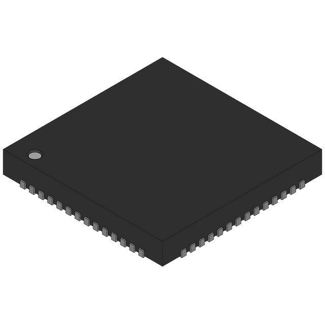
Device Information(1)
PART NUMBER
PACKAGE
TLC5957
QFN (56)
BODY SIZE (NOM)
8.0 mm × 8.0 mm
(1) For all available packages, see the orderable addendum at
the end of the datasheet.
4 Typical Application Circuit (Multiple Daisy Chained TLC5957s)
VLED
SW
COM n
COM n
VLED
SW
COM 1
COM 1
VLED
SW
COM 0
COMSEL 0
COMSEL 1
COMSEL n
COM 0
DATA
SCLK
Controller
LAT
GCLK
FLAGS
READ
X 48
X 48
OUTR0
OUTB15
SIN
OUTR0
IC1
LAT
OUTB15
SIN
SOUT
TLC5957
VCC
SCLK
SOUT
TLC5957
SCLK
ICn
LAT
VCC
GCLK
VCC
VCC
GCLK
Thermal
Pad
IREF
Thermal
Pad
IREF
IREFGND
IREFGND
GND
GND
GND
GND
3
1
An IMPORTANT NOTICE at the end of this data sheet addresses availability, warranty, changes, use in safety-critical applications,
intellectual property matters and other important disclaimers. PRODUCTION DATA.
�TLC5957
SLVSCQ4 – OCTOBER 2014
www.ti.com
Table of Contents
1
2
3
4
5
6
7
8
Features ..................................................................
Applications ...........................................................
Description .............................................................
Typical Application Circuit (Multiple Daisy
Chained TLC5957s)................................................
Revision History.....................................................
Pin Configuration and Functions .........................
Specifications.........................................................
1
1
1
7.1
7.2
7.3
7.4
7.5
7.6
7.7
4
4
5
5
5
7
8
Absolute Maximum Ratings ......................................
Handling Ratings ......................................................
Recommended Operating Conditions.......................
Thermal Information .................................................
Electrical Characteristics...........................................
Timing Requirements ...............................................
Typical Characteristics ..............................................
8.2 Test Circuit .............................................................. 10
9
Detailed Description ............................................ 11
9.1 Overview ................................................................. 11
9.2 Functional Block Diagram ....................................... 12
9.3 Device Functional Modes........................................ 13
1
2
3
4
10 Application and Implementation........................ 17
10.1 Application Information.......................................... 17
11 Power Supply Recommendations ..................... 17
12 Layout................................................................... 17
12.1 Layout Guidelines ................................................. 17
12.2 Layout Example .................................................... 18
13 Device and Documentation Support ................. 18
13.1
13.2
13.3
13.4
Parameter Measurement Information ................ 10
Related Links ........................................................
Trademarks ...........................................................
Electrostatic Discharge Caution ............................
Glossary ................................................................
18
18
18
18
14 Mechanical, Packaging, and Orderable
Information ........................................................... 18
8.1 Pin Equivalent Input and Output Schematic
Diagrams.................................................................. 10
5 Revision History
2
DATE
REVISION
NOTES
October 2014
*
Initial release.
Submit Documentation Feedback
Copyright © 2014, Texas Instruments Incorporated
�TLC5957
www.ti.com
SLVSCQ4 – OCTOBER 2014
6 Pin Configuration and Functions
55 54 53 52 51 50 49
48 47
OUTR10
VCC
OUTB10
OUTG10
OUTG11
OUTR11
OUTR12
OUTB11
OUTB12
OUTG12
OUTG13
OUTR13
IREFGND
56
1
OUTB13
RTQ
56 PINS
Top View
46 45 44 43
42
SOUT
OUTR14
2
41
OUTB9
OUTG14
3
40
OUTG9
OUTB14
4
39
OUTR9
OUTR15
5
38
OUTB8
OUTG15
6
37
OUTG8
OUTB15
7
36
OUTR8
OUTR0
8
35
OUTB7
OUTG0
9
34
OUTG7
OUTB0
10
33
OUTR7
OUTR1
11
32
OUTB6
OUTG1
12
31
OUTG6
OUTB1
13
30
OUTR6
OUTR2
14
29
GCLK
LAT
27 28
SCLK
SIN
OUTB5
OUTR5
23 24 25 26
OUTG5
OUTB4
OUTG4
OUTR4
OUTB3
20 21 22
OUTG3
17 18 19
OUTB2
15 16
OUTR3
Thermal
PAD
(Solder side)
(GND terminal)
OUTG2
IREF
Pin Functions
PIN
I/O
DESCRIPTION
NAME
NO.
GCLK
29
GND
ThermalPad
—
Power ground. The thermal pad must be soldered to GND on PCB.
IREF
1
—
Maximum constant-current value setting. The OUTR0 to OUTB15 maximum constant output
current are set to the desired values by connecting an external resistor between IREF and
IREFGND. See Equation 1 for more detail. The external resistor should be placed close to the
device.
IREFGND
56
—
Analog ground. Dedicated ground pin for the external IREF resistor. This pin should be connected
to analog ground trace which is connected to power ground near the common GND point of board.
LAT
27
I
The LAT falling edge latches the data from the common shift register into the GS data latch or FC
data latch.
OUTR0R15
8, 11, 14, 17, 20,
23, 30, 33, 36,
39, 44, 47, 50,
53, 2, 5
O
Constant current output for RED LED. Multiple outputs can be tied together to increase the
constant current capability. Different voltages can be applied to each output. These outputs are
turned on-off by GCLK signal and the data in GS data memory.
OUTG0G15
9, 12, 15, 18, 21,
24, 31, 34, 37,
40, 45, 48, 51,
54, 3, 6
O
Constant current output for GREEN LED. Multiple outputs can be tied together to increase the
constant current capability. Different voltages can be applied to each output. These outputs are
turned on-off by GCLK signal and the data in GS data memory.
OUTB0B15
10, 13, 16, 19,
22, 25, 32, 35,
38, 41, 46, 49,
52, 55, 4, 7
O
Constant current output for BLUE LED. Multiple outputs can be tied together to increase the
constant current capability. Different voltages can be applied to each output. These outputs are
turned on-off by GCLK signal and the data in GS data memory.
I
Grayscale(GS) pulse width modulation (PWM) reference clock control for OUTXn.
Each GCLK rising edge increase the GS counter by1 for PWM control.
Copyright © 2014, Texas Instruments Incorporated
Submit Documentation Feedback
3
�TLC5957
SLVSCQ4 – OCTOBER 2014
www.ti.com
Pin Functions (continued)
PIN
I/O
DESCRIPTION
NAME
NO.
SCLK
28
I
Serial data shift clock. Data present on SIN are shifted to the 48-bit common shift register LSB
with the SCLK rising edge. Data in the shift register are shifted towards the MSB at each SCLK
rising edge.
The common shift register MSB appears on SOUT.
SIN
26
I
Serial data input of the 48-bit common shift register.
When SIN is high level, the LSB is set to '1' for only one SCLK input rising edge. If two SCLK
rising edges are input while SIN is high, then the 48-bit shift register LSB and LSB+1 are set to '1'.
When SIN is low, the LSB is set to '0' at the SCLK input rising edge.
SOUT
42
O
Serial data output of the 48-bit common shift register. SOUT is connected to the MSB of the
register.
VCC
43
—
Power-supply voltage.
7 Specifications
7.1 Absolute Maximum Ratings
over operating free-air temperature range (unless otherwise noted)
VCC
(2)
MIN
MAX
–0.3
6.0
V
OUTx0 to OUTx15, x = R, G, B
30
30
mA
SIN, SCLK, LAT, GCLK, IREF
–0.3
VCC + 0.3
V
SOUT
–0.3
VCC + 0.3
V
OUTx0 to OUTx15, x = R, G, B
–0.3
11
V
–40
150
°C
Supply voltage
VCC
IOUT
Output current (dc)
VIN (2)
Input voltage range
VOUT
(2)
TJ(MAX)
(1)
(2)
Output voltage range
(1)
Operation junction temperature
UNIT
Stresses beyond those listed under Absolute Maximum Ratings may cause permanent damage to the device. These are stress ratings
only, which do not imply functional operation of the device at these or any other conditions beyond those indicated under Recommended
Operating Conditions. Exposure to absolute-maximum-rated conditions for extended periods may affect device reliability.
All voltage values are with respect to device ground terminal.
7.2 Handling Ratings
Tstg
V(ESD)
(1)
(2)
4
MIN
MAX
UNIT
–55
150
°C
Human body model (HBM), per ANSI/ESDA/JEDEC JS-001, all pins (1)
–3
3
Charged device model (CDM), per JEDEC specification JESD22-C101, all
pins (2)
–1
1
Storage temperature range
Electrostatic discharge
kV
JEDEC document JEP155 states that 500-V HBM allows safe manufacturing with a standard ESD control process.
JEDEC document JEP157 states that 250-V CDM allows safe manufacturing with a standard ESD control process.
Submit Documentation Feedback
Copyright © 2014, Texas Instruments Incorporated
�TLC5957
www.ti.com
SLVSCQ4 – OCTOBER 2014
7.3 Recommended Operating Conditions
At TA = –40°C to 85°C, unless otherwise noted.
MIN
NOM
MAX
UNIT
DC CHARACTERISTICS VCC = 3 V to 5.5 V
VCC
Supply voltage
VO
Voltage applied to output
OUTx0 to OUTx15, x = R, G, B
3
VIH
High level input voltage
SIN, SCLK, LAT, GCLK
VIL
Low level input voltage
SIN, SCLK, LAT, GCLK
IOH
High level output current
SOUT
IOL
Low level output current
SOUT
5.5
V
10
V
0.7×VCC
VCC
V
GND
0.3×VCC
V
–2
mA
2
mA
OUTx0 to OUTx15, x = R, G, B, 3V ≤ VCC ≤ 4V
20
OUTx0 to OUTx15, x = R, G, B, 4V < VCC ≤ 5.5V
25
IOLC
Constant output sink current
mA
TA
Operating free air temperature
–40
85
°C
TJ
Operation junction temperature
–40
125
°C
AC CHARACTERISTICS, VCC = 3 V to 5.5 V
FCLK(SCLK)
Data shift clock frequency
SCLK
33
MHz
FCLK(GCLK)
Grayscale control clock frequency
GCLK
33
MHz
7.4 Thermal Information
TLC5957
THERMAL METRIC (1)
RθJA
Junction-to-ambient thermal resistance
27.4
RθJC(top)
Junction-to-case (top) thermal resistance
13.6
RθJB
Junction-to-board thermal resistance
5.5
ψJT
Junction-to-top characterization parameter
0.2
ψJB
Junction-to-board characterization parameter
5.5
RθJC(bot)
Junction-to-case (bottom) thermal resistance
0.8
(1)
UNIT
RTQ (56 PINS)
°C/W
For more information about traditional and new thermal metrics, see the IC Package Thermal Metrics application report, SPRA953.
7.5 Electrical Characteristics
over operating free-air temperature range (unless otherwise noted)
PARAMETER
VOH
TEST CONDITIONS
High
IOH = –2mA at SOUT
Low
IOL = 2mA at SOUT
Output voltage
VOL
MIN
TYP
VCC-0.4
MAX
UNIT
VCC
V
0.4
V
VLOD0
LODVTH = 00b
0.05
0.09
0.15
V
VLOD1
LODVTH = 01b
0.15
0.19
0.25
V
VLOD2
LODVTH = 10b
0.3
0.35
0.4
V
VLOD3
LODVTH = 11b
0.45
0.49
0.55
V
1.184
1.209
1.234
V
1
µA
LED open detection threshold
VIREF
Reference voltage output
RIREF = 5.97kΩ (1mA target), BC = 0h, CCR/G/B = 80h
IIN
Input current (SIN, SCLK, LAT, GCLK)
VIN = VCC or GND
–1
ICC0
SIN/SCLK/LAT/GSCLK = GND, GSn = 0000h, BC = 4h, CCR/G/B = 120h,
VOUTn = 0.6V, RIREF = OPEN, VCC = 4V
8
10
ICC1
SIN/SCLK/LAT/GSCK = GND, GSn = 0000h, BC = 4h, CCR/G/B = 120h,
VOUTn = 0.6V, RIREF = 7.5kΩ (Io = 10mA target) , VCC = 4V
11
13
SIN/SCLK/LAT = GND, GCLK = 33MHz, TSU3 = 200ns, XREFRESH = 0,
GSn = FFFFh, BC = 4h, CCR/G/B = 120h, VOUTn = 0.6V,
RIREF = 7.5kΩ (Io = 10mA target) , VCC = 4V
20
26
ICC3
SIN/SCLK/LAT = GND, GCLK = 33MHz, TSU3 = 200ns, XREFRESH = 0,
GSn = FFFFh, BC = 7h, CCR/G/B = 1D2h, VOUTn = 0.6V,
RIREF = 7.5kΩ (Io = 25mA target) , VCC = 4V
22
28
ICC4
In power save mode
0.9
1.5
ICC2
Supply current (VCC)
Copyright © 2014, Texas Instruments Incorporated
Submit Documentation Feedback
mA
5
�TLC5957
SLVSCQ4 – OCTOBER 2014
www.ti.com
Electrical Characteristics (continued)
over operating free-air temperature range (unless otherwise noted)
PARAMETER
TEST CONDITIONS
MIN
TYP
MAX
±1%
±3%
±1%
±2%
UNIT
Δ IOLC0
Constant current error
(OUTx0-15, x = R/G/B)
Channel-tochannel (1)
All OUTn = on, BC = 0h, CCR/G/B = 08Fh, VOUTn = VOUTfix = 0.6V,
RIREF = 7.5kΩ(1mA target), TA = +25C, at same color grouped output of
OUTR0-15, OUTG0-15 and OUTB0-15
ΔIOLC1
Constant current error
(OUTx0-15, x = R/G/B)
Device-todevice (2)
All OUTn = on, BC = 0h, CCR/G/B = 08Fh, VOUTn = VOUTfix = 0.6V,
RIREF = 7.5kΩ(1mA target), TA = +25C, at same color grouped output of
OUTR0-15, OUTG0-15 and OUTB0-15
Δ IOLC2
Line regulation (3)
VCC = 3.0 to 5.5V, All OUTn = on, BC = 0h, CCR/G/B = 08Fh,
VOUTn = VOUTfix = 0.6V, RIREF = 7.5kΩ (1mA target)
±1
±3
%/V
ΔIOLC3
Load regulation (4)
VCC = 4V, All OUTn = on, BC = 0h, CCR/G/B = 08Fh, VOUTn = 0.6 to 3V,
VOUTfix = 1V, RIREF = 7.5kΩ (1mA target)
±1
±3
%/V
ΔIOLC4
Constant current error
(OUTx0-15, x = R/G/B)
Channel-tochannel (1)
All OUTn = on, BC = 7h, CCR/G/B - 1CCh, VOUTn = VOUTfix = 0.6V,
RIREF = 7.5kΩ(25mA target), TA = +25C, at same color grouped output of
OUTR0-15, OUTG0-15 and OUTB0-15
±1%
±3%
ΔIOLC5
Constant current error
(OUTx0-15, x = R/G/B)
Device-todevice (2)
All OUTn = on, BC = 7h, CCR/G/B - 1CCh, VOUTn = VOUTfix = 0.6V,
RIREF = 7.5kΩ(25mA target), TA = +25C, at same color grouped output of
OUTR0-15, OUTG0-15 and OUTB0-15
±1%
±3%
ΔIOLC6
Line regulation (3)
VCC = 3.0 to 5.5V, All OUTn = on, BC = 7h, CCR/G/B - 1CCh,
VOUTn = VOUTfix = 0.6V, RIREF = 7.5kΩ (25mA target)
±1
±3
%/V
Δ IOLC7
Load regulation (4)
All OUTn = on, BC = 7h, CCR/G/B - 1CCh, VOUTn = 0.6 to 3V,
VOUTfix = 0.6V, RIREF = 7.5kΩ (25mA target)
±1
±3
%/V
TTSD
Thermal shutdown threshold
170
180
°C
THYS
Thermal shutdown hysterisis
VISP(in)
VISP(out)
(1)
10
°C
IREF resistor short protection threshold
0.190
V
IREF resistor short-protection release
threshold
0.330
V
The deviation of each outputs in same color group (OUTR0~15 or OUTG0~15 or OUTB0~15) from the average of same color group
constant current. The deviation is calculated by the formula. (X = R or G or B, n = 0~15
æ
ç
D (%) = ç
ç
è
(2)
160
IOUTXn
(IOUTX0 + IOUTX1 + ... + IOUTX14 + IOUTX15)
16
ö
÷
- 1÷ ´ 100
÷
ø
The deviation of the average of constant-current in each color group from the ideal constant-current value. (X = R or G or B) :
æ (IOUTX0 + IOUTX1 + ... + IOUTX15 )
ö
- (Ideal Output Current) ÷
ç
16
D (%) = ç
÷ ´ 100
Ideal Output Current
çç
÷÷
è
ø
Ideal current is calculated by the following equation:
æ VIREF ö
÷÷ ´
çR
è IREF ( W ) ø
Ideal Output (mA ) = Gain ´ ç
(3)
100
æ (IOUTXn at VCC = 5.5V ) - (IOUTXn at VCC = 3.0V ) ö
ç
÷´
(IOUTXn at VCC = 3.0V
è
ø 5.5V - 3V
Load regulation is calculated by the following equation. (X = R or G or B, n = 0~15):
D (% / V ) =
6
VIREF = 1.209V(Typ), refer to Table 1 for the Gain at chosen BC.
Line regulation is calculated by the following equation. (X = R or G or B, n = 0~15):
D (% / V ) =
(4)
CCR(or CCG, CCB) / 511d,
æ (IOUTXn at VOUTXn = 3V ) - (IOUTXn at VOUTXn
ç
(IOUTXn at VOUTXn = 1V
è
Submit Documentation Feedback
= 1V ) ö
100
÷´
ø 3V - 1V
Copyright © 2014, Texas Instruments Incorporated
�TLC5957
www.ti.com
SLVSCQ4 – OCTOBER 2014
7.6 Timing Requirements
At TA = –40°C to 85°C, unless otherwise noted.
MIN
TYP
MAX
UNIT
AC CHARACTERISTICS, VCC = 3 V to 5.5 V
tWH0
SCLK
10
ns
tWL0
SCLK
10
ns
GCLK
10
ns
tWL1
GCLK
10
ns
tWH2
LAT
10
ns
tSU0
SIN – SCLK↑
2
ns
tWH1
Pulse duration
tSU1
3
ns
LAT↓ – SCLK↑ , for WRTGS, WRTFC, and TMGST Command
20
ns
LAT↓ – SCLK↑ , for LATGS, READFC, and LINERESET Command
80
ns
tSU3
LAT↓ – GCLK↑ , for LATGS AND LINERESET Command
30
ns
tH0
SCLK↑ – SIN
2
ns
tH1
SCLK↑ – LAT↑
2
ns
tH2
SCLK↓ – LAT↓
2
ns
tSU2
LAT↑ – SCLK↑
Setup time
tWHO , tWL0 , tWH1, tWL1, tWH2
VCC
INPUT
50%
GND
t wl
t wh
tSU0 , tSU1 , tSU2 , tSU3 , tH0 , t1
VCC
CLOCK
INPUT
(1)
50%
GND
tSU
tH
VCC
DATA/CONTROL
INPUT
(1)
50%
GND
tH2
LAT
S CLK
1
2
3
1022 1023 1024
1
2
3
4
5
tH2
LAT Signal needs to include falling edge of SCLK
Figure 1. Input Timing
Copyright © 2014, Texas Instruments Incorporated
Submit Documentation Feedback
7
�TLC5957
SLVSCQ4 – OCTOBER 2014
www.ti.com
7.7 Typical Characteristics
At VCC= 4V and TA = 25°C, unless otherwise noted.
50
50
1 mA
5 mA
10 mA
20 mA
45
40
Output Current (mA)
35
30
25
20
15
35
30
25
20
15
10
10
5
5
0
0
0
0.2
0.4
0.6
Output Voltage (V)
0.8
1
0
0.2
0.4
0.6
Output Voltage (V)
D001
VCC = 4 V
Figure 2. Output Current vs Output Voltage
D003
3
1 mA
5 mA
10 mA
20 mA
2
1 mA
5 mA
10 mA
20 mA
2
1
OUTG15
OUTG14
OUTG13
OUTG12
Output Current (Ch)
D005
VCC = 4 V
OUTG11
OUTG9
OUTG10
OUTG8
OUTR6
OUTG5
OUTG4
OUTG0
OUTR15
OUTR14
OUTR13
OUTR12
Output Current (Ch)
OUTR11
OUTR9
OUTR10
OUTR8
OUTR7
OUTR6
OUTR5
-3
OUTR4
-3
OUTR3
-2
OUTR2
-2
OUTR1
-1
OUTR0
-1
OUTG3
0
OUTG2
0
OUTG1
'IOLC (%)
1
'IOLC (%)
1
Figure 3. Output Current vs Output Voltage
3
D006
VCC = 4 V
Figure 4. Constant-Current Error vs Output Current
(Channel-to-Channel in RED color group)
Figure 5. Constant-Current Error vs Output Current
(Channel-to-Channel in GREEN color group)
3
1.4
1 mA
5 mA
10 mA
20 mA
2
1 mA
25 mA
1.3
1.2
1
1.1
' IOLC (%)
'IOLC (%)
0.8
VCC = 5 V
OUTG7
Output Current (mA)
40
1 mA
5 mA
10 mA
20 mA
25 mA
45
0
-1
1
0.9
0.8
0.7
-2
0.6
Output Current (Ch)
0.5
-40
OUTB15
OUTB14
OUTB13
OUTB12
OUTB11
OUTB10
OUTB9
OUTB8
OUTB7
OUTB6
OUTB5
OUTB4
OUTB3
OUTB2
OUTB1
OUTB0
-3
D007
-20
0
20
40
60
80
100
Ambient Temperature (qC)
VCC=4V
120
140
D014
VOUTXn=0.6V
VCC = 4 V
Figure 6. Constant-Current Error vs Output Current
(Channel-to-Channel in BLUE color group)
8
Submit Documentation Feedback
Figure 7. Maximum Constant-Current Error vs Ambient
Temperature
(Channel-to-Channel in RED color group)
Copyright © 2014, Texas Instruments Incorporated
�TLC5957
www.ti.com
SLVSCQ4 – OCTOBER 2014
Typical Characteristics (continued)
At VCC= 4V and TA = 25°C, unless otherwise noted.
1.4
1.6
1 mA
25 mA
1.4
1
' IOLC (%)
' IOLC (%)
1.2
1
0.8
0.8
0.6
0.6
0.4
0.4
0.2
-40
-20
0
20
40
60
80
100
Ambient Temperature (qC)
VCC=4V
120
0.2
-40
140
-20
0
D015
20
40
60
80
100
Ambient Temperature (qC)
VOUTXn=0.6V
VCC=4V
Figure 8. Maximum Constant-Current Error vs Ambient
Temperature
(Channel-to-Channel in GREEN color group)
120
140
D016
VOUTXn=0.6V
Figure 9. Maximum Constant-Current Error vs Ambient
Temperature
(Channel-to-Channel in BLUE color group)
25
30
1 mA
5 mA
10 mA
20 mA
25 mA
20
VCC = 3 V
VCC = 4 V
VCC = 5.5 V
24
Supply Current (mA)
25
Output Current (mA)
1 mA
25 mA
1.2
15
10
23
22
21
20
19
5
18
0
17
0
1
2
3
4
5
Step [dec]
6
7
8
0
5
10
15
Output Current (mA)
VOUTXn=0.6V,
GCLK=33MHz,
D012
Figure 10. Global Brightness Control Linearity
20
25
D017
GSXn=FFFFh,
Figure 11. Supply Current (ICC) vs Output Current
21.5
Supply Current (mA)
21.25
21
20.75
20.5
20.25
20
VCC = 3 V
VCC = 4 V
VCC = 5.5 V
19.75
19.5
-50
GCLK=33MHz
GSXn=FFFFh,
0
50
100
Ambient Temperature (qC)
VOUTXn=0.6V,
150
D013
Output Current=10mA,
Figure 12. Supply Current vs Ambient Temperature
Copyright © 2014, Texas Instruments Incorporated
Submit Documentation Feedback
9
�TLC5957
SLVSCQ4 – OCTOBER 2014
www.ti.com
8 Parameter Measurement Information
8.1 Pin Equivalent Input and Output Schematic Diagrams
VCC
VCC
OUTPUT
INPUT
GND
GND
Figure 13. SIN, SCLK
Figure 14. SOUT
VCC
OUTXn
(1)
(1) X=R or G or B, n=0~15
INPUT
GND
GND
Figure 16. OUTR0/G0/B0 through OUTR15/G15/B15
Figure 15. LAT, GCLK
8.2 Test Circuit
RL
VCC
VCC
OUTXn
VCC
VLED
(2)
VCC
SOUT
(1)
GND
(1)
CL
GND
CL
(1) CL includes measurement probe and jig capacitance.
(1) CL includes measurement probe and jig capacitance.
(2) X=R or G or B, n=0~15
Figure 17. Rise Time and Fall Time Test Circuit for OUTXn
VCC
VCC
Figure 18. Rise Time and Fall Time Test Circuit for SOUT
OUTR0
OUTXn
(1)
VOUTXn
GND OUTB15
(1)
VOUTfix
(1) X=R or G or B, n=0~15
Figure 19. Constant Current Test Circuit for OUTXn
10
Submit Documentation Feedback
Copyright © 2014, Texas Instruments Incorporated
�TLC5957
www.ti.com
SLVSCQ4 – OCTOBER 2014
9 Detailed Description
9.1 Overview
The TLC5957 is a 48-channel constant-current sink driver for multiplexing an LED display system. Each channel
has an individually-adjustable, 65536-step, pulse width modulation (PWM) grayscale control.
The TLC5957 supports output current range from 1 mA to 25 mA. Channel-to-channel accuracy is 3% max,
device-to-device accuracy is 2% max in all current ranges. Also, the TLC5957 implements Low Grayscale
Enhancement (LGSE) technology to improve the display quality at low grayscale conditions. These features
improve the performance of the TLC5957-multiplexed display system.
The output channels are grouped in three groups, each group has 16 channels for one color. Each group has a
512-step color brightness control (CC) function. The maximum current value of all 48 channels can be set by 8step global brightness control (BC) function. GS, CC and BC data are accessible via a serial interface port.
The TLC5957 has one error flag: LED open detection (LOD), that can be read via a serial interface port. The
TLC5957 also has an enhanced circuit to solve the caterpillar issue caused by open LEDs. Thermal shutdown
(TSD) and Iref resistor short protection (ISP) assure TLC5957 of a higher system reliability.
Copyright © 2014, Texas Instruments Incorporated
Submit Documentation Feedback
11
�TLC5957
SLVSCQ4 – OCTOBER 2014
www.ti.com
9.2 Functional Block Diagram
VCC
48 bit LOD
DATA LATCH
LSB
MSB
SIN
SOUT
48 bit Common Shift Register
SEL_TD0
SCLKB
SCLK
47
0
48
767
ADR
48
LSB
Grayscale (GS)
XRST
data latch
Address Counter
GS first data
latch for
OUTR/G/B0
ADR Select
LAT16B
48
48
0
LOAD
48
48
47 48
48
MSB
GS first data GS first data
latch for
latch for
OUTR/G/B14 OUTR/G/B15
GS first data
latch for
OUTR/G/B1
95 97
48
48
48
671 672
48
719 720
48
767
48
LAT768B
LSB
LAT
Command
Decoder
MSB
LATFC
2nd 48ch GS Data Latch for Display
0
767
48
XRST
48
48
48
SCLK
SCLKB
LAT
ES-PWN Timing Control
XRFESH
Poker Trans
Mode
2
1
48
PWM Mode
LSB
Power On
Reset
XRST
Function Control (FC) Data latch
0
47
42
GSCLK
2 XRFRESH
GCLK EDGE
Internal circuit
1st line and
Quick pulse
LSB
MSB
16 bit
GS Counter
3rd GS Data Latch for ES-PWN Synch
34
48
0
47
GDLY
32
12-grouped Switching Delay
48
BC & CC & PCHG
2
IREF
48
48
5
3
PRIODEND
48
MSB
48CH Constant driver with 3 bit BC, 27 bit CC
and Pre-charge FET
Reference
Current Control
48
Detection
Voltage
GND
LOD Detection
OUTR
OUTR15
OUTG0
OUTB0
12
Submit Documentation Feedback
OUTR1
OUTG15
OUTB15
Copyright © 2014, Texas Instruments Incorporated
�TLC5957
www.ti.com
SLVSCQ4 – OCTOBER 2014
9.3 Device Functional Modes
After power on, all OUTXn of TLC5957 are turned off. All the internal counters and function control registers are
initialized. Below is a brief summary of the sequence to operate TLC5957, just give users a general idea how this
part works. After that, the function block related to each step will be detailed in following sections.
1. According to required LED current, choose BC and CC code, select the current programming resistor RIREF.
2. Send WRTFC command to set FC register value if the default value need be changed.
3. Write GS data of line 1 into GS data latch. Using LATGS command for the last group of 48bit GS data
loading, the GS data written just now will be displayed.
4. Input GCLK continuously, 2N GCLK (N>=9) as a segment. Between the interval of two segments, supply
voltage should be switched from one line to next line accordingly.
5. During the same period of step4, GS data for next line should be written into GS data latch. Using LATGS
command for the last group of 48bit GS data loading.
6. Repeat step 4-5 until it comes to the last line for a multiplexing panel. Input 2N GCLK (N>=9) as a segment,
at the same time, GS data for 1st line should be written into GS data latch. Using LINERESET command for
the last group of 48bit GS data loading.
Repeat step 4 through 6.
9.3.1 Brightness Control (BC) Function
The TLC5957 is able to adjust the output current of all constant-current outputs simultaneously. This function is
called global brightness control (BC). The global BC for all outputs is programmed with a 3-bit word, thus all
output currents can be adjusted in 8 steps from 12.9% to 100% (See Table 2) for a given current programming
resistor(RIREF)
BC data can be set via the serial interface. When the BC data change, the output current also changes
immediately. When the device is powered on, the BC data in the function control (FC) register is set to 4h as the
initial value.
9.3.2 Color Control (CC) Function
The TLC5957 is able to adjust the output current of each of the three color groups OUTR0-OUTR15, OUTG0OUTG15, and OUTB0-OUTB15 separately. This function is called color brightness control (CC). For each color,
it has 9-bit data latch CCR, CCG, or CCB in FC register. Thus, all color group output currents can be adjusted in
512 steps from 0% to 100% of the maximum output current, IOLCMax. (See next section for more details about
IOLCMax). The CC data are entered via the serial interface. When the CC data change, the output current also
changes immediately.
When the IC is powered on, the CC data are set to ‘100h’.
Equation 1 calculates the actual output current.
Iout(mA) = IOLCMax(mA) × ( CCR/511d or CCB/511d)
(1)
Where:
IOLCMax = the maximum channel current for each channel, determined by BC data and RIREF (See Equation 2)
CCR/G/B = the color brightness control value for each color group in the FC1 register (000h to 1FFh)
Table 1 shows the CC data versus the constant-current against IOLCMax.
Copyright © 2014, Texas Instruments Incorporated
Submit Documentation Feedback
13
�TLC5957
SLVSCQ4 – OCTOBER 2014
www.ti.com
Device Functional Modes (continued)
Table 1. CC Data vs Current Ratio and Set Current Value
RATIO OF OUTPUT
CURRENT
TO IolcMax(%, typical)
CC DATA (CCR or CCG or CCB)
OUTPUT CURRENT (mA, RIREF = 7.41 kΩ)
BC = 7h
(IolcMax =25mA)
BC = 0h
(IolcMax=3.2mA)
BINARY
DECIMAL
HEX
0 0000 0000
0
00
0
0
0
0 0000 0001
1
01
0.2
0.05
0.006
0 0000 0010
2
02
0.4
0.10
0.013
—
—
—
—
—
—
1 0000 0000
(Default)
256
(Default)
100
(Default)
50.1
12.52
1.621
—
—
—
—
—
—
1 1111 1101
509
1FD
99.6
24.90
3.222
1 1111 1110
510
1FE
99.8
24.95
3.229
1 1111 1111
511
1FF
100.0
25
3.235
9.3.3 Select RIREF For a Given BC
The maximum output current per channel, IOLCMax is determined by resistor RIREF placed between the IREF and
IREFGND pins, and the BC code in FC register. The voltage on IREF is typically 1.209V. RIREF can be calculated
by Equation 2.
Riref(kΩ) = Viref(V) / IOLCMax(mA) × Gain
(2)
Where:
VIREF = the internal reference voltage on IREF (1.209V, typical)
IOLCMax is the largest current for each output at CCR/G/B=1FFh.
Gain = the current gain at a selected BC code (See Table 2 )
Table 2. Current Gain Versus BC Code
BC DATA
GAIN
RATIO OF
GAIN / GAIN_MAX (AT MAX BC)
0 (recommend)
20.0
12.9%
001
1
39.5
25.6%
010
2
58.6
37.9%
011
3
80.9
52.4%
100 (default)
4 (default)
100.0
64.7%
101
5
113.3
73.3%
110
6
141.6
91.7%
111
7
154.5
100%
BINARY
HEX
000 (recommend)
NOTE: Recommend to use smaller BC code for better performance. For noise immunity purposes, suggest RIREF < 60 kΩ.
9.3.4 Choosing BC/CC For a Different Application
BC is mainly used for global brightness adjustment between day and night. Suggested BC is 4h, which is in the
middle of the range; thus, one can change brightness up and down flexibly.
CC can be used to fine tune the brightness in 512 steps, this is suitable for white balance adjustment between
RGB color groups. To get a pure white color, the general requirement for the luminous intensity ratio of R, G, B
LED is 3:6:1. Depending on LED’s characteristics (Electro-Optical conversion efficiency), the current ratio of R,
G, B LED will be much different from this ratio. Usually, the Red LED will need the largest current. One can
choose 511d(the max value) CC code for the color group which needs the largest current at first, then choose
proper CC code for the other two color groups according to the current ratio requirement of the LED used.
14
Submit Documentation Feedback
Copyright © 2014, Texas Instruments Incorporated
�TLC5957
www.ti.com
SLVSCQ4 – OCTOBER 2014
9.3.4.1 Example 1: Red LED Current is 20mA, Green LED Needs 12mA, Blue LED needs 8mA
1. Red LED needs the largest current, so choose 511d for CCR
2. 511 x 12mA / 20mA = 306.6, thus choose 307d for CCG. With same method, choose 204d for CCB.
3. According to the required red LED current, choose 7h for BC.
4. According to Equation 2, RIREF = 1.2V/20mA x 154.5 = 9.27 kΩ
In this example, we choose 7h for BC, instead of using the default 4h. This is because the Red LED current is
20mA, approaching the upper limit of current range. To prevent the constant output current from exceeding the
upper limit in case a larger BC code is input accidently, we choose the maximum BC code here.
9.3.4.2 Example 2: Red LED Current is 5mA, Green LED Needs 2mA, Blue LED Needs 1mA.
1. Red LED needs the largest current, so choose 511d for CCR.
2. 511 x 2mA / 5mA = 204.4, thus choose 204d for CCG. With same method, choose 102d for CCB.
3. According to the required blue LED current, choose 0h for BC.
4. According to Equation 2, RIREF = 1.2V / 5mA x 20 = 4.8 kΩ
In this example, we choose 0h for BC, instead of using the default 4h. This is because the Blue LED current is
1mA, which is approaching the lower limit of current range. To prevent the constant output current from
exceeding the lower limit in case a lower BC code is input accidently, we choose the min BC code here.
In general, if LED current is in the middle of range(i.e, 10mA), one can just use the default 4h as BC code.
9.3.5 LED Open Detection (LOD)
LOD function detects a fault caused by an open circuit in any LED string, or a short from OUTXn to ground with
low impedance, by comparing the OUTXn voltage to the LOD detection threshold voltage level set by LODVLT in
the FC register. If the OUTXn voltage is lower than the programmed voltage, the corresponding output LOD bit
will be set to '1' to indicate a opened LED. Otherwise, the output of that LOD bit is '0'. LOD data output by the
detect circuit are valid only during the ‘on’ period of that OUTXn output channel. LOD data are always ‘0’ for
outputs that are turned off.
9.3.6 Poker Mode
Poker Mode provides the TLC5957 with a flexible PWM bit, from 9 bit to 16 bit. Therefore, data length can be
reduced. In high multiplexing applications, Poker Mode can significantly increase visual refresh rate.
9.3.7 Internal Circuit for Caterpillar Removal
Caterpillar effect is a very common issue on LED panels. It is usually caused by an LED lamp open, LED lamp
leakage or LED lamp short. The TLC5957 implements an internal circuit that can eliminate the caterpillar issue
caused by LED open. This function can be enabled and disabled by LINERESET command. If the function is
enabled, the IC automatically detects the broken LED lamp, and the lamp will not light until IC reset.
9.3.8 Internal Pre-charge FET for Ghost Removal
The internal pre-charge FET can prevent ghosting of multiplexed LED modules. One cause of this phenomenon
is the charging current for parasitic capacitance of the OUTXn through the LED when the supply voltage switches
from one common line to the next common line.
To prevent this unwanted charging current, the TLC5957 uses an internal FET to pull OUTXn up to VCC-1.4V
during the common line switching period. Thus, no charging current flows through LED and the ghosting is
eliminated.
9.3.9 Thermal Shutdown (TSD)
The thermal shutdown (TSD) function turns off all IC constant-current outputs when the junction temperature (TJ)
exceeds 170°C (typ). It resumes normal operation when TJ falls below 160°C (typ).
Copyright © 2014, Texas Instruments Incorporated
Submit Documentation Feedback
15
�TLC5957
SLVSCQ4 – OCTOBER 2014
www.ti.com
9.3.10 IREF Resistor Short Protection (ISP)
The Iref resistor short protection (ISP) function prevents unwanted large currents from flowing though the
constant-current output when the Iref resistor is shorted accidently. The TLC5957 turns off all output channels
when the Iref pin voltage is lower than 0.19V (typ). When the Iref pin voltage goes higher than 0.33V (typ), the
TLC5957 resumes normal operation.
9.3.11 Noise Reduction
Large surge currents may flow through the IC and the board on which the device is mounted if all 48 LED
channels turn on simultaneously at the 1st GCLK rising edge. This large surge current could induce detrimental
noise and electromagnetic interference (EMI) into other circuits.
The TLC5957 separate the LED channels into 12 groups. Each group turns on sequentially with some delay
between one group and the next group. By this means, a soft-start feature is provided and the inrush current is
minimized.
16
Submit Documentation Feedback
Copyright © 2014, Texas Instruments Incorporated
�TLC5957
www.ti.com
SLVSCQ4 – OCTOBER 2014
10 Application and Implementation
NOTE
Information in the following applications sections is not part of the TI component
specification, and TI does not warrant its accuracy or completeness. TI’s customers are
responsible for determining suitability of components for their purposes. Customers should
validate and test their design implementation to confirm system functionality.
10.1 Application Information
Send request via email for Application Note: Build High Density, High Refresh Rate, Multiplexing LED Panel with
TLC5957
11 Power Supply Recommendations
The VCC power supply voltage should be decoupled by placing a 0.1 µF ceramic capacitor close to VCC pin and
GND plane. Depending on panel size, several electrolytic capacitors must be placed on board equally distributed
to get a well regulated LED supply voltage (VLED). VLED voltage ripple should be less than 5% of its nominal
value. Furthermore, the VLED should be set to the voltage calculated by equation:
VLED > Vf + 0.4V (10mA constant current example)
(3)
Where: Vf = maximum forward voltage of LED
12 Layout
12.1 Layout Guidelines
1. Place the decoupling capacitor near the VCC pin and GND plane.
2. Place the current programming resistor Riref close to IREF pin and IREFGND pin.
3. Route the GND pattern as widely as possible for large GND currents. Maximum GND current is
approximately 1.2A
4. Routing between the LED cathode side and the device OUTXn pin should be as short and straight as
possible to reduce wire inductance.
5. The PowerPAD™ must be connected to GND plane because the pad is used as power ground pin internally,
there will be large current flow through this pad when all channels turn on. Furthermore, this pad should be
connected to a heat sink layer by thermal via to reduce device temperature. One suggested thermal via
pattern is shown as below. For more information about suggested thermal via pattern and via size, see "
PowerPAD Thermally Enhanced Package", SLMA002G.
Copyright © 2014, Texas Instruments Incorporated
Submit Documentation Feedback
17
�TLC5957
SLVSCQ4 – OCTOBER 2014
www.ti.com
12.2 Layout Example
13 Device and Documentation Support
13.1 Related Links
The table below lists quick access links. Categories include technical documents, support and community
resources, tools and software, and quick access to sample or buy.
Table 3. Related Links
PARTS
PRODUCT FOLDER
SAMPLE & BUY
TECHNICAL
DOCUMENTS
TOOLS &
SOFTWARE
SUPPORT &
COMMUNITY
TLC5957
Click here
Click here
Click here
Click here
Click here
13.2 Trademarks
PowerPAD is a trademark of Texas Instruments.
13.3 Electrostatic Discharge Caution
These devices have limited built-in ESD protection. The leads should be shorted together or the device placed in conductive foam
during storage or handling to prevent electrostatic damage to the MOS gates.
13.4 Glossary
SLYZ022 — TI Glossary.
This glossary lists and explains terms, acronyms, and definitions.
14 Mechanical, Packaging, and Orderable Information
The following pages include mechanical, packaging, and orderable information. This information is the most
current data available for the designated devices. This data is subject to change without notice and revision of
this document. For browser-based versions of this data sheet, refer to the left-hand navigation.
18
Submit Documentation Feedback
Copyright © 2014, Texas Instruments Incorporated
�PACKAGE OPTION ADDENDUM
www.ti.com
10-Dec-2020
PACKAGING INFORMATION
Orderable Device
Status
(1)
Package Type Package Pins Package
Drawing
Qty
Eco Plan
(2)
Lead finish/
Ball material
MSL Peak Temp
Op Temp (°C)
Device Marking
(3)
(4/5)
(6)
TLC5957RTQR
ACTIVE
QFN
RTQ
56
2000
RoHS & Green
NIPDAU
Level-3-260C-168 HR
-40 to 85
5957AB
TLC5957RTQT
ACTIVE
QFN
RTQ
56
250
RoHS & Green
NIPDAU
Level-3-260C-168 HR
-40 to 85
5957AB
(1)
The marketing status values are defined as follows:
ACTIVE: Product device recommended for new designs.
LIFEBUY: TI has announced that the device will be discontinued, and a lifetime-buy period is in effect.
NRND: Not recommended for new designs. Device is in production to support existing customers, but TI does not recommend using this part in a new design.
PREVIEW: Device has been announced but is not in production. Samples may or may not be available.
OBSOLETE: TI has discontinued the production of the device.
(2)
RoHS: TI defines "RoHS" to mean semiconductor products that are compliant with the current EU RoHS requirements for all 10 RoHS substances, including the requirement that RoHS substance
do not exceed 0.1% by weight in homogeneous materials. Where designed to be soldered at high temperatures, "RoHS" products are suitable for use in specified lead-free processes. TI may
reference these types of products as "Pb-Free".
RoHS Exempt: TI defines "RoHS Exempt" to mean products that contain lead but are compliant with EU RoHS pursuant to a specific EU RoHS exemption.
Green: TI defines "Green" to mean the content of Chlorine (Cl) and Bromine (Br) based flame retardants meet JS709B low halogen requirements of