�������
�
� �
� �� �
� ���� ��
��������
SWRS025C − APRIL 2004 − REVISED JULY 2007
D Hot Plug Protection
D Quad 1.0 to 2.5 Gigabits Per Second (Gbps)
Serializer/Deserializer
D Independent Channel Operation
D 2.5-V Power Supply for Low Power
D
D
D
D
Operation
Selectable Signal Preemphasis for Serial
Output
Interfaces to Backplane, Copper Cables, or
Optical Converters
Lock Indication and Sync Mode for Fast
Initialization
18-Bit Parallel Buses for Flexible Interface
Applications
D On-Chip PLL Provides Clock Synthesis
D
D
D
D
D
D
From Low-Speed Reference
Receiver Differential Input Thresholds
200 mV Min
Rated for Industrial Temperature Range
Typical Power: 1700 mW at 2.5 Gbps
Ideal for High-Speed Backplane
Interconnect and Point-to-Point Data Link
Internal Passive Receive Equalization
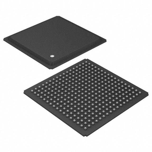
Small Footprint 19 mm x 19 mm, 289-Ball
PBGA Package
description
The TLK4250 device is a four-channel, multi-gigabit transceiver used in high-speed bidirectional point-to-point
data transmission systems. The four channels in the transceiver are configured as four separate links. The
transceiver supports an effective serial interface speed of 1.0 Gbps to 2.5 Gbps per channel, providing up to
2.25 Gbps of data bandwidth per channel.
The primary application of the transceiver is to provide high-speed I/O data channels for point-to-point baseband
data transmission over controlled impedance media of approximately 50 Ω. The transmission media can be a
printed-circuit board, copper cables, or fiber-optic cable. The maximum rate and distance of data transfer
depend on the attenuation characteristics of the media and the noise coupling to the environment.
The transceiver can also replace parallel data transmission architectures by providing a reduction in the number
of traces, connector pins, and transmit/receive pins. Parallel data loaded into the transmitter is delivered to the
receiver over a serial channel, which can be a coaxial copper cable, a controlled impedance backplane, or an
optical link. The data is then reconstructed into its original parallel format. It offers significant power and cost
savings over current solutions, as well as scalability for higher data rate in the future.
The transceiver performs the data parallel-to-serial and serial-to-parallel conversions. The clock extraction
functions as a physical layer interface device. The serial transceiver interface operates at a maximum data rate
of 2.5 Gbps. Each transmitter latches 18-bit parallel data at a rate based on the supplied reference clock
(GTx_CLK). The 18-bit parallel data is internally encoded into 20 bits by framing the 18-bit data with start and
stop bits. The resulting 20-bit frame is then transmitted differentially at 20 times the reference clock (GTx_CLK)
rate.
The receiver section performs the serial-to-parallel conversion on the input data, synchronizing the resulting
20-bit wide parallel data to the recovered clock (Rx_CLK). It then extracts the 18 bits of data from the 20-bit wide
data resulting in 18 bits of parallel data at the receive data terminals (RDx[0:17]). This results in an effective data
payload of 0.9 Gbps to 2.25 Gbps (18 bits data x GTx_CLK frequency) per channel.
The transceiver provides an internal loopback capability for self-test purposes. Serial data from the serializer
is passed directly to the deserializer, allowing the protocol device a functional self-check of the physical
interface.
Please be aware that an important notice concerning availability, standard warranty, and use in critical applications of
Texas Instruments semiconductor products and disclaimers thereto appears at the end of this data sheet.
PowerPAD is a trademark of Texas Instruments.
Copyright 2004 − 2007, Texas Instruments Incorporated
���� ����� �
�
����!"#���� �� $%!!&�� #� �� �%�'�$#���� (#�&
�!�(%$�� $����!" �� ��&$���$#����� �&! �)& �&!"� �� �&*#� ����!%"&���
��#�(#!( +#!!#��,
�!�(%$���� �!�$&����- (�&� ��� �&$&��#!�', ��$'%(&
�&����- �� #'' �#!#"&�&!�
WWW.TI.COM
1
��������
�
� �
� �� �
� ���� ��
��������
SWRS025C − APRIL 2004 − REVISED JULY 2007
The transceiver is designed to be hot plug capable. An on-chip power-on reset circuit holds the Rx_CLK low
during power up. This circuit also places the parallel side output signal terminals, DOUTTxP and DOUTTxN,
into a high-impedance state during power up.
The transceiver uses a 2.5-V supply. The I/O section is 3-V compatible. With the 2.5-V supply, the transceiver
is power efficient, consuming less than 1700 mW typically. The transceiver is characterized for operation from
−40°C to 85°C.
AVAILABLE OPTIONS
PACKAGE
TA
−40°C to 85°C
PLASTIC BALL GRID ARRAY
(PBGA)
SYMBOL
TLK4250IGPV
TLK4250IZPV
ECAT
NOTE: For the most current package and ordering information, see the Package Option
Addendum at the end of this document, or see the TI website at www.ti.com.
2
WWW.TI.COM
��������
�
� �
� �� �
� ���� ��
��������
SWRS025C − APRIL 2004 − REVISED JULY 2007
17
A
B
TDB1
TDB0
C
D
E
DOUTTB
DOUTTB
PREEMP
P
N
HB
F
G
H
J
K
DINRBP
DINRBN
RDB0
GND
TDC0
L
M
N
DOUTTC
DOUTTC
PREEMP
P
N
HC
P
R
T
U
DINRCP
DINRCN
RDC0
RDC1
17
16
TDB4
TDB2
GNDA
GNDA
VDDAB
GNDA
GNDA
RDB1
VDD
TDC1
GNDA
GNDA
VDDAC
GNDA
GNDA
RDC2
RDC4
16
15
TDB5
TDB3
GND
RDB3
VDDAB
RDB2
GND
VDD
GND
VDD
GND
TDC2
VDDAC
VDD
GND
RDC3
RDC5
15
14
TDB7
TDB6
VDD
RB_CLK
RDB7
RDB4
RDB5
RDB6
GND
TDC5
TDC6
TDC7
TDC4
TDC3
GND
RDC6
RDC7
14
13
TDB8
GND
RDB17
RDB13
RDB10
RDB9
RDB8
VDD
TDC9
TDC10
TDC11
TDC14
VDD
RDC8
RC_CLK
13
TDC12
TDC13
TDC16
GND
RDC10
RDC9
12
GND
RDC13
RDC11
11
GTB_
GTC_
CLK
CLK
LOOPEN
12
TDB9
TDB10
VDD
SYNCB
RDB16
RDB14
RDB12
RDB11
VDD
TDC8
C
TESTEN
11
TDB11
TDB13
GND
VDD
LOCKBB
RDB15
GND
GND
GND
GND
GND
TDC15
VDD
C
10
TDB12
GND
LOOPEN
ENABLE
TESTEN
B
B
B
TDB17
GND
VDD
TDB15
GND
GND
GND
GND
GND
GND
GND
GND
GND
GND
TDC17
SYNCC
RDC17
RDC14
GND
RDC12
10
LOCKBC
GND
RDC16
RDC15
VDD
9
TDD5
TDD1
TDD0
8
GND
GNDA
ENABLE
9
TDB14
TDB16
GND
C
8
GTD_
RDA0
RDA1
VDD
RDA6
RDA8
RDA11
GND
GND
GND
GND
GND
TDD8
VDD
CLK
DOUTTD
7
DINRAN
GNDA
GND
RDA5
RDA9
RDA12
GND
GND
GND
GND
GND
TDD12
TDD9
TDD6
7
P
6
DINRAP
GNDA
RDA2
RDA4
RDA10
RDA14
PREEMP
VDDAA
5
VDDAA
RDA7
RDA13
ENABLE
A
D
DOUTTD
TDD17
LOCKB
ENABLE
A
A
TDD15
GNDA
RDA3
RA_CLK
RDA17
SYNCA
SYNCD
VDD
TDD2
GNDA
6
TDD16
TDD11
TDD4
VDDAD
5
VDDAD
LOOPEN
RDD17
LOCKBD
TDD14
TDD3
VDD
GNDA
DINRDP
4
VDD
GND
GND
GNDA
DINRDN
3
D
A
DOUTTA
3
TDD7
HD
TDA17
VDD
N
TDD10
N
LOOPEN
DOUTTA
TDD13
PREEMP
GND
RDA16
HA
4
TESTEN
RDA15
TESTEN
GNDA
GND
VDD
GND
VDD
GND
TDA15
RDD16
RDD15
GND
P
D
GTA_
2
TDA0
TDA2
TDA3
TDA6
TDA10
TDA13
GND
TDA16
RDD14
RDD13
RDD10
RDD8
RDD6
RDD3
RDD2
RDD0
2
1
CLK
1
TDA1
TDA4
TDA5
TDA7
TDA8
TDA9
TDA11
TDA12
TDA14
RDD12
RDD11
RDD9
RD_CLK
RDD7
RDD5
RDD4
RDD1
A
B
C
D
E
F
G
H
J
K
L
M
N
P
R
T
U
WWW.TI.COM
3
��������
�
� �
� �� �
� ���� ��
��������
SWRS025C − APRIL 2004 − REVISED JULY 2007
functional block diagram
A detailed block diagram of each channel is shown below. Channels A, B, C, and D are identical and are
configured as four separate links.
LOOPENx
DOUTTxP
18-Bit
Register
TDx[0:17]
DOUTTxN
18
Start/Stop
Encoder
20
Parallel to
Serial
Bit
Clock
PREEMPHx
Multiplying
Clock
Synthesizer
GTx_CLK
Controls:
PLL, Bias,
Rx, Tx
TESTENx
ENABLEx
Bit
Clock
Interpolator and
Clock Recovery
MUX
Recovered
Clock
LOCKBx
RDx[0:17]
18-Bit
Register
Rx_CLK
18
Start/Stop
Decoder
20
Serial to
Parallel
MUX
DINRxP
DINRxN
4
WWW.TI.COM
��������
�
� �
� �� �
� ���� ��
��������
SWRS025C − APRIL 2004 − REVISED JULY 2007
Terminal Functions
TERMINAL
NAME
NO.
DINRAP
DINRAN
A6
A7
DINRBP
DINRBN
F17
G17
DINRCP
DINRCN
P17
R17
DINRDP
DINRDN
U4
U3
DOUTTAP
DOUTTAN
A3
A4
DOUTTBP
DOUTTBN
C17
D17
DOUTTCP
DOUTTCN
L17
M17
DOUTTDP
DOUTTDN
U7
U6
ENABLEA
H5
ENABLEB
E10
ENABLEC
M9
ENABLED
J6
GTA_CLK
E2
GTB_CLK
B13
GTC_CLK
K13
GTD_CLK
P8
SYNCA
F4
SYNCB
D12
SYNCC
N10
SYNCD
K5
LOOPENA
H4
LOOPENB
D10
LOOPENC
P12
LOOPEND
M4
LOCKBA
G5
LOCKBB
E11
LOCKBC
N9
LOCKBD
L4
PREEMPHA
A5
PREEMPHB
E17
PREEMPHC
N17
PREEMPHD
U5
TYPE
Input
DESCRIPTION
Serial receive inputs. DINRxP and DINRxN together are the differential serial
inputs that interface from a copper or an optical I/F module.
Output
(high-z
power up)
Serial transmit outputs. DOUTTxP and DOUTTxN are differential serial outputs
that interface to copper or an optical I/F module. These terminals transmit NRZ
data at a rate of 20 times the GTx_CLK value. DOUTTxP and DOUTTxN are
put in a high-impedance state when LOOPENx is high and are active when
LOOPENx is low. During power-on reset these terminals are high impedance.
Input
(w/pullup)
Device enable. When this terminal is held low, the device is placed in
power-down mode. When asserted high while the device is in power-down
mode, the transceiver goes into power-on reset before beginning normal
operation.
Input
Reference clock. GTx_CLK is a continuous external input clock that
synchronizes the transmitter interface TDx. The frequency range of GTx_CLK
is 50 MHz to 125 MHz.
The transmitter uses the rising edge of this clock to register the 18-bit input
data (TDx) for serialization.
Input
(w/pulldown)
Fast synchronization. When asserted high, the transmitter substitutes the
18-bit pattern 111111111000000000 so that when the start/stop bits are framed
around the data, the receiver can immediately detect the proper deserialization
boundary. This is typically used during initialization of the serial link.
Input
(w/pulldown)
Loop enable. When LOOPENx is active high, the internal loop-back path is
activated. The transmitted serial data is directly routed internally to the inputs
of the receiver. This provides a self-test capability with the protocol device. The
DOUTTxP and DOUTTxN outputs are held in a high-impedance state during
the loop-back test. LOOPENx is held low during standard operational state
with external serial outputs and inputs active.
Output
Receiver lock. When this signal is asserted low, it indicates that the receiver
has acquired bit synchronization on the data stream and has located the
start/stop bits so that the deserialized data presented on the parallel receive
bus is properly received.
Input
Preemphasis. When asserted, the serial transmit outputs have extra output
swings on the first bit of any run length of save value bits. If the run length of
output bits is one, then that bit has larger output swings.
WWW.TI.COM
5
��������
�
� �
� �� �
� ���� ��
��������
SWRS025C − APRIL 2004 − REVISED JULY 2007
Terminal Functions (Continued)
TERMINAL
NAME
NO.
RDA[0:17]
A8, B8, C6, C4, D6, D7, D8,
D5, E8, E7, E6, F8, F7, E5,
F6, G6, F5, E4
RDB[0:17]
H17, H16, F15, D15, F14,
G14, H14, E14, H13, G13,
F13, H12, G12, E13, F12,
F11, E12, D13
RDC[0:17]
T17, U17, T16, T15, U16,
U15, T14, U14, T13, U12,
T12, U11, U10, T11, R10,
T9, R9, P10
RDD[0:17]
U2, U1, T2, R2, T1, R1, P2,
P1, N2, M1, M2, L1, K1, L2,
K2, K3, J3, K4
RA_CLK
D4
RB_CLK
D14
RC_CLK
U13
RD_CLK
N1
TDA[0:17]
A2, A1, B2, C2, B1, C1, D2,
D1, E1, F1, F2, G1, H1, G2,
J1, H3, J2, J4
TDB[0:17]
B17, A17, B16, B15, A16,
A15, B14, A14, A13, A12,
B12, A11, A10, B11, A9,
C10, B9, D9
TDC[0:17]
K17, K16, M15, P14, N14,
K14, L14, M14, K12, L13,
M13, N13, L12, M12, P13,
M11, N12, M10
TDD[0:17]
U8, T8, R6, P4, P5, R8, P7,
P6, M8, N7, N6, N5, M7, M6,
N4, L6, M5, K6
TESTENA
H6
TESTENB
F10
TESTENC
P11
TESTEND
M3
TYPE
DESCRIPTION
Output (hi-z
on power up)
Receive data bus. These outputs carry 18-bit parallel data output from the
transceiver to the protocol device, synchronized to Rx_CLK. The data is
valid on the rising edge of Rx_CLK as shown in Figure 7. These terminals
are high-impedance during power-on reset.
Output (low
on power up)
Recovered clock. Output clock that is synchronized to RDx. Rx_CLK is the
recovered serial data rate clock divided by 20. Rx_CLK is held low during
power-on reset.
Input
Transmit data bus. These inputs carry the 18-bit parallel data output from a
protocol device to the transceiver for encoding, serialization, and
transmission. This 18-bit parallel data is clocked into the transceiver on the
rising edge of GTx_CLK as shown in Figure 6.
Input
(w/pulldown)
Test mode enable. This terminal must be left unconnected or tied low.
POWER
VDD
VDDAA
6
C8, C12, C14, D3, D11, F3,
F9, G4, H15, J12, J13, J16,
K15, L5, N3, N8, N11, P15,
R4, R13, U9
Supply
Digital logic power. Provides power for all digital circuitry and digital I/O
buffers.
Supply
Analog power. VDDAx provides a supply reference for the high-speed
receiver and transmitter analog circuits.
B5, C5
VDDAB
E15, E16
VDDAC
N15, N16
VDDAD
R5, T5
WWW.TI.COM
��������
�
� �
� �� �
� ���� ��
��������
SWRS025C − APRIL 2004 − REVISED JULY 2007
Terminal Functions (Continued)
TERMINAL
NAME
TYPE
NO.
DESCRIPTION
GROUND
GNDA
GND
B3, B4, B6, B7, C16, D16,
F16, G16, L16, M16, P16,
R16, T3, T4, T6, T7
Ground
Analog ground. GNDA provides a ground reference for the high-speed
receiver and transmitter analog circuits.
B10, C3, C7, C9, C11, C13,
C15, E3, E9, G3, G7, G8,
G9, G10, G11, G15, H2, H7,
H8, H9, H10, H11, J5, J7, J8,
J9, J10, J11, J14, J15, J17,
K7, K8, K9, K10, K11, L3, L7,
L8, L9, L10, L11, L15, P3,
P9, R3, R7, R11, R12, R14,
R15, T10
Ground
Digital logic ground. Provides a ground for the logic circuits and digital I/O
buffers.
transmit interface
The transmitter portion registers valid incoming 18-bit-wide data (TDx[0:17]) on the rising edge of GTx_CLK.
The data is then framed with start and stop bits, serialized, and transmitted sequentially over the differential
high-speed I/O channel. The clock multiplier multiplies the reference clock (GTx_CLK) by a factor of 10, creating
a bit clock. This internal bit clock is fed to the parallel-to-serial shift register, which transmits data on both the
rising and falling edges of the bit clock providing a serial data rate that is 20 times the reference clock. Data is
transmitted LSB (TDx0) first.
transmit data bus
The transmit bus interface accepts 18-bit-wide, single-ended, TTL parallel data at the TDx[0:17] terminals. Data
is valid on the rising edge of GTx_CLK. The GTx_CLK is used as the word clock. The data and clock signals
must be properly aligned as shown in Figure 1. Detailed timing information can be found in the TTL input
electrical characteristics table.
GTx_CLK
TDXn
tsu
th
Figure 1. Transmit Timing Waveform
transmission latency
The data transmission latency of the transceiver is defined as the delay from the initial 18-bit word on the parallel
transmit interface to the serial transmission of the start bit of the 20-bit frame containing the 18-bit word. The
transmit latency is fixed once the link is established. However, due to silicon process variations and
implementation variables, such as supply voltage and temperature, the exact delay varies slightly. Figure 2
illustrates the timing relationship between the transmit data bus, GTx_CLK, and the serial transmit terminals.
WWW.TI.COM
7
��������
�
� �
� �� �
� ���� ��
��������
SWRS025C − APRIL 2004 − REVISED JULY 2007
Transmitted 20-Bit Frame
DOUTTxP,
DOUTTxN
td(Tx latency)
TDx[0:17]
18-Bit Word to Transmit
GTx_CLK
Figure 2. Transmitter Latency
start/stop framing logic
All true serial interfaces require a method of encoding to ensure minimum transition density so that the receiving
PLL has a minimal number of transitions in which to stay locked onto the data stream. The signal encoding also
provides a mechanism for the receiver to identify the word boundary for correct deserialization. The TLK4250
transceiver wraps a start bit (1) and a stop bit (0) around the 18-bit data payload as shown in Figure 3. This is
transparent to the user, as the transceiver internally adds the framing bits to the data such that the user reads
and writes actual 18-bit data.
20-Bit Frame
18-Bit Word
Stop
Bit
Start
Bit
TDx0
TDx1
...
TDx16
TDx17
Stop
Bit
Start
Bit
Figure 3. Serial Output Data Stream With Start and Stop Bit
parallel-to-serial
The parallel-to-serial shift register takes in the 20-bit-wide frame multiplexed from the framing logic and converts
it to a serial stream. The shift register is clocked on both the rising and falling edges of the internally generated
bit clock, which is 10 times the GTx_CLK input frequency. The LSB (TDx0) is first out after the start bit as shown
in Figure 3.
high-speed data output
The high-speed data output driver consists of a PECL-compatible differential pair that can be optimized for a
particular transmission line impedance and length. The line can be directly coupled or ac coupled. See Figure 10
and Figure 11 for termination details. No external pullup or pulldown resistors are required.
The transceiver provides a selectable signal preemphasis option for driving lossy media. When signal
preemphasis is enabled, the first bit of a run length of same-value bits (e.g., 111...) is driven to a larger output
swing, which precompensates for signal inter-symbol interference (ISI) in lossy media, such as copper cables
or printed circuit board traces.
8
WWW.TI.COM
��������
�
� �
� �� �
� ���� ��
��������
SWRS025C − APRIL 2004 − REVISED JULY 2007
receive interface
The receiver portion of the TLK4250 accepts 20-bit framed differential serial data. The interpolator and clock
recovery circuit locks to the data stream and extracts the bit rate clock. This recovered clock retimes the input
data stream. The serial data is then aligned to the 20-bit frame by finding the start and stop bits and the 18-bit
data is output on a 18-bit wide parallel bus synchronized to the extracted receive clock (Rx_CLK).
receive data bus
The receive bus interface drives 18-bit-wide, single-ended, TTL parallel data at the RDx[0:17] terminals. Data
is valid on the rising edge of Rx_CLK. The Rx_CLK is used as the recovered word clock. The data and clock
signals are aligned as shown in Figure 4. Detailed timing information can be found in the TTL output switching
characteristics table.
Rx_CLK
RDx[0:17]
tsu
th
Figure 4. Receive Timing Waveform
data reception latency
The serial-to-parallel data receive latency is the time from when the start bit arrives at the receiver until the output
of the aligned parallel word. The receive latency is fixed once the link is established. However, due to silicon
process variations and implementation variables, such as supply voltage and temperature, the exact delay
varies slightly. Figure 5 illustrates the timing relationship between the serial receive terminals, the recovered
word clock (Rx_CLK), and the receive data bus.
20-Bit Encoded Frame
DINTxP,
DINTxN
R(latency)
RDx[0:17]
18-Bit Decoded Word
Rx_CLK
Figure 5. Receiver Latency
serial-to-parallel
Serial data is received on the DINRxP and DINRxN terminals. The interpolator and clock recovery circuit locks
to the data stream if the clock to be recovered is within ±100 PPM of the internally generated bit rate clock. The
recovered clock retimes the input data stream. The serial data is then clocked into the serial-to-parallel shift
registers.
WWW.TI.COM
9
��������
�
� �
� �� �
� ���� ��
��������
SWRS025C − APRIL 2004 − REVISED JULY 2007
synchronization mode
The deserializer must synchronize to the serializer in order to receive valid data. Synchronization can be
accomplished in one of two ways.
rapid synchronization
The serializer has the capability to send specific SYNC patterns consisting of 9 ones and 9 zeros, switching at
the input clock rate. The transmission of SYNC patterns enables the deserializer to lock to the serializer signal
within a deterministic time frame. The transmission of SYNC patterns is selected via the SYNC input on the
serializer. On receiving a valid SYNC pulse (wider than 6 clock cycles), 1026 cycles of SYNC pattern are sent.
When the deserializer detects edge transitions at the serial input, it attempts to lock to the embedded clock
information. The deserializer LOCKBx output remains inactive while its clock/data recovery (CDR) locks to the
incoming data or SYNC patterns present on the serial input. When the deserializer locks to the serial data, the
LOCKBx output goes active. When LOCKBx is active, the deserializer outputs represent incoming serial data.
One approach is to tie the deserializer LOCKBx output directly to the SYNCx input of the transmitter. This
ensures that enough SYNC patterns are sent to achieve deserializer lock.
random lock synchronization
The deserializer can attain lock to a data stream without requiring the serializer to send special SYNC patterns.
This allows the transceiver to operate in open-loop applications. Equally important is the deserializer’s ability
to support hot insertion into a running backplane. In the open-loop or hot-insertion case, it is assumed the data
stream is essentially random. Therefore, because lock time varies due to data stream characteristics, the exact
lock time cannot be predicted. The primary constraint on the random lock time is the initial phase relation
between the incoming data and the GTx_CLK when the deserializer powers up.
The data contained in the data stream can also affect lock time. If a specific pattern is repetitive, the deserializer
could enter false lock—falsely recognizing the data pattern as the start/stop bits. This is referred to as repetitive
multitransition (RMT). This occurs when more than one low-high transition takes place per clock cycle over
multiple clock cycles. In the worst case, the deserializer could become locked to the data pattern rather than
the clock. Circuitry within the deserializer can detect that the possibility of false lock exists. On detection, the
circuitry prevents the LOCKBx from becoming active until the potential false-lock pattern changes. Notice that
the RMT pattern only affects the deserializer lock time, and once the deserializer is in lock, the RMT pattern does
not affect the deserializer state as long as the same data boundary happens each cycle. The deserializer does
not go into lock until it finds a unique data boundary that consists of four consecutive cycles of data boundary
(start/stop bits) at the same position.
The deserializer stays in lock until it cannot detect the same data boundary (start/stop bits) for four consecutive
cycles. Then the deserializer goes out of lock and hunts for the new data boundary (start/stop bits). In the event
of loss of synchronization, the LOCKBx terminal output goes inactive and the outputs (including Rx_CLK) enter
a high-impedance state. The user’s system must monitor the LOCKBx terminal in order to detect a loss of
synchronization. On detection of loss of lock, sending SYNC patterns for resynchronization is desirable if
reestablishing lock within a specific time is critical. However, the deserializer can lock to random data as
previously noted. LOCKBx is held inactive for at least nine cycles after loss of lock is detected.
recommended power-up sequence
When powering up the device, it is recommended to first set the ENABLEx terminal low. Set the ENABLEx
terminal to high once sufficient time has passed to allow the power supply to stabilize.
power-down mode
When the ENABLEx terminal is deasserted low, the transceiver goes into a power-down mode. In the
power-down mode, the serial transmit terminals (DOUTTxP, DOUTTxN) and the receive data bus terminals
(RDx[0:17]) go into a high-impedance state.
10
WWW.TI.COM
��������
�
� �
� �� �
� ���� ��
��������
SWRS025C − APRIL 2004 − REVISED JULY 2007
reference clock input
The reference clock (GTx_CLK) is an external input clock that synchronizes the transmitter interface. The
reference clock is then multiplied in frequency 10 times to produce the internal serialization bit clock. The internal
serialization bit clock is frequency locked to the reference clock and clocks out the serial transmit data on both
its rising and falling edges, providing a serial data rate that is 20 times the reference clock.
The receiver tracking logic uses clock phases from the internal PLL as it aligns the recovered clock phase with
the incoming serial data stream; therefore, the input reference clock (GTX_CLK) is needed even if the transmit
function of the TLK4250 is not being used. The receiver function has the ability to track an incoming serial data
stream that is within ±200 ppm of the data rate that is set by GTX_CLK. This allows the use of clock sources
with ±100 ppm frequency tolerance.
operating frequency range
The transceiver may operate at a serial data rate between 1.0 Gbps to 2.5 Gbps. GTx_CLK must be within
±100 PPM of the desired parallel data rate clock. Each individual channel may operate at a different rate.
testability
The transceiver has a comprehensive suite of built-in self-tests. The loopback function provides for at-speed
testing of the transmit/receive portions of the circuitry. The ENABLEx terminal allows for all circuitry to be
disabled so that a quiescent current test can be performed.
loop-back testing
The transceiver can provide a self-test function by enabling (LOOPENx) the internal loop-back path. Enabling
this terminal causes serial transmitted data to be routed internally to the receiver. The parallel data output can
be compared to the parallel input data for functional verification. (The external differential output is held in a
high-impedance state during the loop-back testing.)
power-on reset
On application of minimum valid power, the transceiver generates a power-on reset. During the power-on reset,
the RDx terminals are 3-stated and Rx_CLK is held low. The length of the power-on reset cycle depends on the
GTx_CLK frequency, but is less than 1 ms in duration.
WWW.TI.COM
11
��������
�
� �
� �� �
� ���� ��
��������
SWRS025C − APRIL 2004 − REVISED JULY 2007
absolute maximum ratings over operating free-air temperature (unless otherwise noted)†
Supply voltage, VDD (see Note 1) . . . . . . . . . . . . . . . . . . . . . . . . . . . . . . . . . . . . . . . . . . . . . . . . . . . . . . . . . . . . −0.3 V to 3 V
Voltage range at TDx, ENABLEx, GTx_CLK, LOOPENx, SYNCx, PREEMPHx . . . . . . . . . . . . . . . . −0.3 V to 4 V
Voltage range at any other terminal except above . . . . . . . . . . . . . . . . . . . . . . . . . . . . . . . . −0.3 V to VDD + 0.3 V
Package power dissipation, PD . . . . . . . . . . . . . . . . . . . . . . . . . . . . . . . . . . . . . . . . . . See Dissipation Rating Table
Storage temperature, Tstg . . . . . . . . . . . . . . . . . . . . . . . . . . . . . . . . . . . . . . . . . . . . . . . . . . . . . . . . . . −65°C to 150°C
Electrostatic discharge . . . . . . . . . . . . . . . . . . . . . . . . . . . . . . . . . . . . . . . . . . . . . . . . . . . . . . . . . . . . . . . . . HBM: 2 kV
Characterized free-air operating temperature range, TA . . . . . . . . . . . . . . . . . . . . . . . . . . . . . . . . . . −40°C to 85°C
Lead temperature 1,6 mm (1/16 inch) from case for 10 seconds . . . . . . . . . . . . . . . . . . . . . . . . . . . . . . . . . 260°C
† Stresses beyond those listed under “absolute maximum ratings” may cause permanent damage to the device. These are stress ratings only, and
functional operation of the device at these or any other conditions beyond those indicated under “recommended operating conditions” is not
implied. Exposure to absolute-maximum-rated conditions for extended periods may affect device reliability.
NOTE 1: All voltage values, except differential I/O bus voltages, are with respect to network ground.
Air Flow
0 m/s
0.5 m/s
1 m/s
2.5 m/s
TJA (C/W)
18.4
16.92
15.95
14.7
electrical characteristics over recommended operating conditions
PARAMETER
VDD
TA
ICC
PD
TEST CONDITION
Supply voltage
Operating free-air temperature
Supply current
MIN
TYP
MAX
2.3
2.5
2.7
V
85
°C
−40
VDD = 2.5 V, Rate = 1 Gbps, PRBS pattern
VDD = 2.5 V, Rate = 2.5 Gbps, PRBS pattern
UNIT
285
mA
680
Power dissipation
VDD = 2.5 V, Rate = 1 Gbps, PRBS pattern
VDD = 2.5 V, Rate = 2.5 Gbps, PRBS pattern
715
Shutdown current
VDD = 2.7 V, Rate = 2.5 Gbps, worst case pattern†
ENABLEx = 0, VDDA, VDD terminals, VDD = maximum
PLL start-up lock time
VDD, VDDA = 2.3 V, EN ↑ to PLL acquire
1700
mW
2920
µA
520
0.1
Data acquisition time
† Worst case pattern is a pattern that creates a maximum transition density on the serial transceiver.
0.4
1024
ms
bits
reference clock (GTx_CLK) timing requirements over recommended operating conditions (unless
otherwise noted)
PARAMETER
Rω
Frequency
TEST CONDITIONS
TYP
MAX
TYP−0.01%
50
TYP+0.01%
Maximum data rate
TYP−0.01%
125
TYP+0.01%
50%
60%
Frequency tolerance
−100
Duty cycle
40%
Jitter
12
MIN
Minimum data rate
Peak-to-peak
WWW.TI.COM
100
40
UNIT
MHz
ppm
ps
��������
�
� �
� �� �
� ���� ��
��������
SWRS025C − APRIL 2004 − REVISED JULY 2007
TTL input electrical characteristics over recommended operating conditions (unless otherwise
noted)
TTL Signals: TDx0 ... TDx17, GTx_CLK, LOOPENx, SYNCx, PREEMPHx
PARAMETER
TEST CONDITIONS
MIN
TYP
MAX
2
UNIT
VIH
VIL
High-level input voltage
See Figure 6
Low-level input voltage
See Figure 6
3.6
V
0.8
V
IIH
IIL
High-level input current
Low-level input current
VDD = Max, VIN = 2 V
VDD = Max, VIN = 0.4 V
40
µA
CIN
Input capacitance
0.8 V to 2 V
tr
tf
GTx_CLK, TDx rise time
0.8 V to 2 V, C = 5 pF, see Figure 6
1
ns
GTx_CLK, TDx fall time
2 V to 0.8 V, C = 5 pF, see Figure 6
1
ns
tsu
th
TDx setup to ↑ GTx_CLK
See Figure 6
1.5
ns
TDx hold to ↑ GTx_CLK
See Figure 6
0.4
ns
µA
−40
4
pF
3.6 V
2V
GTx_CLK
0.8 V
0V
tr
tf
3.6 V
2V
TDx[0:17]
0.8 V
0V
tsu
tf
tr
th
Figure 6. TTL Data Input Valid Levels for AC Measurements
WWW.TI.COM
13
��������
�
� �
� �� �
� ���� ��
��������
SWRS025C − APRIL 2004 − REVISED JULY 2007
TTL output switching characteristics over recommended operating conditions (unless otherwise
noted)
PARAMETER
TEST CONDITIONS
MIN
TYP
2.1
2.3
GND
0.25
MAX
UNIT
VOH
VOL
High-level output voltage
Low-level output voltage
IOH= −1 mA, VDD = minimum
IOL= 1 mA, VDD = minimum
tr(slew)
tf(slew)
Magnitude of Rx_CLK, RDx slew rate (rising)
0.8 V to 2 V, C = 5 pF, see Figure 7
0.5
V/ns
Magnitude of Rx_CLK, RDx slew rate (falling)
0.8 V to 2 V, C = 5 pF, see Figure 7
0.5
V/ns
tsu
th
RDx setup to ↑ Rx_CLK
RDx hold to ↑ Rx_CLK
V
0.5
V
50% voltage swing, GTx_CLK = 50 MHz,
see Figure 7
8
ns
50% voltage swing, GTx_CLK = 125 MHz,
see Figure 7
3
ns
50% voltage swing, GTx_CLK = 50 MHz,
see Figure 7
8
ns
50% voltage swing, GTx_CLK = 125 MHz,
see Figure 7
3
ns
2V
Rx_CLK
0.8 V
0V
tr(slew)
tf(slew)
2V
RDx[0:17]
0.8 V
0V
tr(slew)
tsu
tf(slew)
th
Figure 7. TTL Data Output Valid Levels for AC Measurements
14
WWW.TI.COM
��������
�
� �
� �� �
� ���� ��
��������
SWRS025C − APRIL 2004 − REVISED JULY 2007
transmitter/receiver characteristics
PARAMETER
TEST CONDITION
MIN
TYP
MAX
UNIT
DC-coupled. Preemphasis = high, see Figure 8
750
1000
1375
DC-coupled. Preemphasis = low, see Figure 8
650
950
1300
DC-coupled. Preemphasis = high, see Figure 8
1500
2000
2750
DC-coupled. Preemphasis = low, see Figure 8
1000
1500
2600
DC-coupled. See Figure 8
500
750
1100
mV
DC-coupled. See Figure 8
1000
1500
2200
mV
1000
1250
1400
mV
VOD(p)
VOD(p) = |VTXP − VTXN|,
Preemphasis VOD
VOD(pp−p)
Differential, peakĆto-peak output
voltage with preemphasis
VOD(d)
VD(d) = |VTXP − VTXN|,
De-emphasis VOD
VOD(pp−d)
Differential, peak-to-peak output
voltage with deemphasis
V(cmt)
Transmit termination voltage range,
(VTXP + VTXN)/2
VID
Receiver input voltage differential
VID= |RXP – RXN|
200
Vcmr
Receiver common-mode voltage
range, (VRXP + VRXN)/2
1000
VDD−350
mV
−10
10
µA
2
pF
Iin
Cin
tr, tf
Receiver input leakage
RL = 50 Ω, CL = 5 pF, see Figure 9
Serial transmit data total jitter
(peak-to-peak)
Differential output jitter, random + deterministic,
223 − 1 PRBS pattern at 2.5 Gbps
Receive jitter tolerance
Total input jitter, PRBS pattern, permitted eye
closure at zero crossing
100
150
ps
0.15
UI
0.5
UI
At 1.0 Gbps
Tlatency
TX latency
Rlatency
RX latency
mV
mV
Receiver input capacitance
Differential output signal rise and
fall time (20% to 80%)
mV
Bit
times
At 2.5 Gbps
At 1.0 Gbps
Bit
times
At 2.5 Gbps
VOD(p)
VOD(d)
VOD(pp-d)
V(cmt)
VOD(pp-p)
tf
tr
VOD(d)
Bit
Time
Bit
Time
VOD(p)
Figure 8. Differential and Common-Mode Output Voltage Definitions
WWW.TI.COM
15
��������
�
� �
� �� �
� ���� ��
��������
SWRS025C − APRIL 2004 − REVISED JULY 2007
80%
DOUTTxP
50%
20%
tr
tf
80%
50%
20%
DOUTTxN
tf
tr
+V
80%
V(cmt)
DOUTTxP−DOUTTxN
20%
−V
tr
tf
Figure 9. Rise and Fall Time Definitions
TXP
RXP
VDD
ZO
ZO
5 kΩ
ZO
7.5 kΩ
ZO
TXN
Transmitter
+
_
GND
RXN
Media
Receiver
Figure 10. High-Speed I/O Directly Coupled Mode
TXP
RXP
VDD
ZO
ZO
5 kΩ
ZO
7.5 kΩ
ZO
TXN
Transmitter
GND
RXN
Media
Receiver
Figure 11. High-Speed I/O AC-Coupled Mode
16
WWW.TI.COM
+
_
��������
�
� �
� �� �
� ���� ��
��������
SWRS025C − APRIL 2004 − REVISED JULY 2007
AC-coupling is only recommended if the parallel TX data stream is encoded to achieve a dc-balanced data
stream. Otherwise, the ac capacitors can induce common-mode voltage drift due to the dc-unbalanced data
stream.
WWW.TI.COM
17
�PACKAGE OPTION ADDENDUM
www.ti.com
5-Jun-2016
PACKAGING INFORMATION
Orderable Device
Status
(1)
Package Type Package Pins Package
Drawing
Qty
Eco Plan
Lead/Ball Finish
MSL Peak Temp
(2)
(6)
(3)
TLK4250GPV
PREVIEW
BGA
GPV
289
TBD
Call TI
Call TI
TLK4250IGPV
OBSOLETE
BGA
GPV
289
TBD
Call TI
Call TI
TLK4250IZPV
LIFEBUY
BGA
ZPV
289
TBD
Call TI
Call TI
Op Temp (°C)
Device Marking
(4/5)
-40 to 85
TLK4250I
-40 to 85
TLK4250I
(1)
The marketing status values are defined as follows:
ACTIVE: Product device recommended for new designs.
LIFEBUY: TI has announced that the device will be discontinued, and a lifetime-buy period is in effect.
NRND: Not recommended for new designs. Device is in production to support existing customers, but TI does not recommend using this part in a new design.
PREVIEW: Device has been announced but is not in production. Samples may or may not be available.
OBSOLETE: TI has discontinued the production of the device.
(2)
Eco Plan - The planned eco-friendly classification: Pb-Free (RoHS), Pb-Free (RoHS Exempt), or Green (RoHS & no Sb/Br) - please check http://www.ti.com/productcontent for the latest availability
information and additional product content details.
TBD: The Pb-Free/Green conversion plan has not been defined.
Pb-Free (RoHS): TI's terms "Lead-Free" or "Pb-Free" mean semiconductor products that are compatible with the current RoHS requirements for all 6 substances, including the requirement that
lead not exceed 0.1% by weight in homogeneous materials. Where designed to be soldered at high temperatures, TI Pb-Free products are suitable for use in specified lead-free processes.
Pb-Free (RoHS Exempt): This component has a RoHS exemption for either 1) lead-based flip-chip solder bumps used between the die and package, or 2) lead-based die adhesive used between
the die and leadframe. The component is otherwise considered Pb-Free (RoHS compatible) as defined above.
Green (RoHS & no Sb/Br): TI defines "Green" to mean Pb-Free (RoHS compatible), and free of Bromine (Br) and Antimony (Sb) based flame retardants (Br or Sb do not exceed 0.1% by weight
in homogeneous material)
(3)
MSL, Peak Temp. - The Moisture Sensitivity Level rating according to the JEDEC industry standard classifications, and peak solder temperature.
(4)
There may be additional marking, which relates to the logo, the lot trace code information, or the environmental category on the device.
(5)
Multiple Device Markings will be inside parentheses. Only one Device Marking contained in parentheses and separated by a "~" will appear on a device. If a line is indented then it is a continuation
of the previous line and the two combined represent the entire Device Marking for that device.
(6)
Lead/Ball Finish - Orderable Devices may have multiple material finish options. Finish options are separated by a vertical ruled line. Lead/Ball Finish values may wrap to two lines if the finish
value exceeds the maximum column width.
Important Information and Disclaimer:The information provided on this page represents TI's knowledge and belief as of the date that it is provided. TI bases its knowledge and belief on information
provided by third parties, and makes no representation or warranty as to the accuracy of such information. Efforts are underway to better integrate information from third parties. TI has taken and
continues to take reasonable steps to provide representative and accurate information but may not have conducted destructive testing or chemical analysis on incoming materials and chemicals.
TI and TI suppliers consider certain information to be proprietary, and thus CAS numbers and other limited information may not be available for release.
Addendum-Page 1
Samples
�PACKAGE OPTION ADDENDUM
www.ti.com
5-Jun-2016
In no event shall TI's liability arising out of such information exceed the total purchase price of the TI part(s) at issue in this document sold by TI to Customer on an annual basis.
Addendum-Page 2
�MECHANICAL DATA
MPBG233 – FEBRUARY 2002
GPV (S–PBGA–N289)
PLASTIC BALL GRID ARRAY
19,20
SQ
18,80
16,00 TYP
1,00
U
T
R
P
1,00
N
M
L
K
J
H
G
F
E
D
A1 Corner
C
B
A
3
1
2
5
4
7
6
9
8
11
10
13
12
15
14
17
16
Bottom View
2,00 MAX
Seating Plane
0,60
0,40
0,10
0,50
0,30
0,15
4204203/A 02/2002
NOTES: A. All linear dimensions are in inches (millimeters).
B. This drawing is subject to change without notice.
POST OFFICE BOX 655303
• DALLAS, TEXAS 75265
1
��IMPORTANT NOTICE
Texas Instruments Incorporated and its subsidiaries (TI) reserve the right to make corrections, enhancements, improvements and other
changes to its semiconductor products and services per JESD46, latest issue, and to discontinue any product or service per JESD48, latest
issue. Buyers should obtain the latest relevant information before placing orders and should verify that such information is current and
complete. All semiconductor products (also referred to herein as “components”) are sold subject to TI’s terms and conditions of sale
supplied at the time of order acknowledgment.
TI warrants performance of its components to the specifications applicable at the time of sale, in accordance with the warranty in TI’s terms
and conditions of sale of semiconductor products. Testing and other quality control techniques are used to the extent TI deems necessary
to support this warranty. Except where mandated by applicable law, testing of all parameters of each component is not necessarily
performed.
TI assumes no liability for applications assistance or the design of Buyers’ products. Buyers are responsible for their products and
applications using TI components. To minimize the risks associated with Buyers’ products and applications, Buyers should provide
adequate design and operating safeguards.
TI does not warrant or represent that any license, either express or implied, is granted under any patent right, copyright, mask work right, or
other intellectual property right relating to any combination, machine, or process in which TI components or services are used. Information
published by TI regarding third-party products or services does not constitute a license to use such products or services or a warranty or
endorsement thereof. Use of such information may require a license from a third party under the patents or other intellectual property of the
third party, or a license from TI under the patents or other intellectual property of TI.
Reproduction of significant portions of TI information in TI data books or data sheets is permissible only if reproduction is without alteration
and is accompanied by all associated warranties, conditions, limitations, and notices. TI is not responsible or liable for such altered
documentation. Information of third parties may be subject to additional restrictions.
Resale of TI components or services with statements different from or beyond the parameters stated by TI for that component or service
voids all express and any implied warranties for the associated TI component or service and is an unfair and deceptive business practice.
TI is not responsible or liable for any such statements.
Buyer acknowledges and agrees that it is solely responsible for compliance with all legal, regulatory and safety-related requirements
concerning its products, and any use of TI components in its applications, notwithstanding any applications-related information or support
that may be provided by TI. Buyer represents and agrees that it has all the necessary expertise to create and implement safeguards which
anticipate dangerous consequences of failures, monitor failures and their consequences, lessen the likelihood of failures that might cause
harm and take appropriate remedial actions. Buyer will fully indemnify TI and its representatives against any damages arising out of the use
of any TI components in safety-critical applications.
In some cases, TI components may be promoted specifically to facilitate safety-related applications. With such components, TI’s goal is to
help enable customers to design and create their own end-product solutions that meet applicable functional safety standards and
requirements. Nonetheless, such components are subject to these terms.
No TI components are authorized for use in FDA Class III (or similar life-critical medical equipment) unless authorized officers of the parties
have executed a special agreement specifically governing such use.
Only those TI components which TI has specifically designated as military grade or “enhanced plastic” are designed and intended for use in
military/aerospace applications or environments. Buyer acknowledges and agrees that any military or aerospace use of TI components
which have not been so designated is solely at the Buyer's risk, and that Buyer is solely responsible for compliance with all legal and
regulatory requirements in connection with such use.
TI has specifically designated certain components as meeting ISO/TS16949 requirements, mainly for automotive use. In any case of use of
non-designated products, TI will not be responsible for any failure to meet ISO/TS16949.
Products
Applications
Audio
www.ti.com/audio
Automotive and Transportation
www.ti.com/automotive
Amplifiers
amplifier.ti.com
Communications and Telecom
www.ti.com/communications
Data Converters
dataconverter.ti.com
Computers and Peripherals
www.ti.com/computers
DLP® Products
www.dlp.com
Consumer Electronics
www.ti.com/consumer-apps
DSP
dsp.ti.com
Energy and Lighting
www.ti.com/energy
Clocks and Timers
www.ti.com/clocks
Industrial
www.ti.com/industrial
Interface
interface.ti.com
Medical
www.ti.com/medical
Logic
logic.ti.com
Security
www.ti.com/security
Power Mgmt
power.ti.com
Space, Avionics and Defense
www.ti.com/space-avionics-defense
Microcontrollers
microcontroller.ti.com
Video and Imaging
www.ti.com/video
RFID
www.ti-rfid.com
OMAP Applications Processors
www.ti.com/omap
TI E2E Community
e2e.ti.com
Wireless Connectivity
www.ti.com/wirelessconnectivity
Mailing Address: Texas Instruments, Post Office Box 655303, Dallas, Texas 75265
Copyright © 2016, Texas Instruments Incorporated
�


 工商网监
湘ICP备2023018690号
工商网监
湘ICP备2023018690号
