�������
��
� �
�������
����
�
SLVS126C − JULY 1995 − REVISED JUNE 1996
D
D
D
D
D
D
D
Wide Bandwidth . . . Typ 100 MHz at −3 dB
Three Channels
0 V to 4 V, Digital Level-Contrast Control
0 V to 4 V, Digital Level-Gain Adjust Control
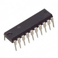
20-Pin Plastic DIP for Small PCB Area
Required
Fewer Peripheral Components Required
Than for LM1203 Applications
Independent CLAMP(+) Adjustment to Each
Channel
N PACKAGE
(TOP VIEW)
R CLAMP(+)
VCC1
R VIDEO IN
R CLAMP CAP
G VIDEO IN
GND
G CLAMP CAP
B VIDEO IN
B CLAMP CAP
CONTRAST
description
1
20
2
19
3
18
4
17
5
16
6
15
7
14
8
13
9
12
10
11
G CLAMP(+)
B CLAMP(+)
R VIDEO OUT
R GAIN ADJUST
VCC2
G VIDEO OUT
G GAIN ADJUST
B VIDEO OUT
B GAIN ADJUST
CLAMP GATE
The TLS1233 is a 100-MHz wide-band video preamplifier system intended for mid-to-high-resolution RGB
(red-green-blue) color monitors. Each video amplifier (R, G, and B) contains a gain set for adjusting maximum
system gain (AV = 7.8 V/V). The TLS1233 provides digital level-operated contrast, brightness, and gain
adjustment control. All the control inputs offer high input impedance and an operation range from 0 V to 4 V for
easy interface to the serial digital buses. Provided in a 20-pin plastic dual-in-line package (DIP), the TLS1233
integrates most of the external components required to accommodate the video system.
The TLS1233 operates from a 12-V supply and contains an internal input bias voltage. Also, the TLS1233
contains the feedback resistor required between output and CLAMP(−) for dc level holding. The device is
characterized for operation from 0°C to 70°C.
functional block diagram
R VIDEO IN
R CLAMP CAP
R GAIN ADJUST
3
16 V
CC2
A1
A2
4
18
17
1
G VIDEO IN 5
G CLAMP CAP 7
A1
A2
15
G GAIN ADJUST 14
20
B VIDEO IN
B CLAMP CAP
8
CLAMP GATE
R CLAMP(+)
G VIDEO OUT
G CLAMP(+)
A1
A2
9
B GAIN ADJUST 12
CONTRAST
R VIDEO OUT
13 B VIDEO OUT
19
10 Contrast
Control
B CLAMP(+)
11
Please be aware that an important notice concerning availability, standard warranty, and use in critical applications of
Texas Instruments semiconductor products and disclaimers thereto appears at the end of this data sheet.
Copyright 1996, Texas Instruments Incorporated
�
� ������ ��� ����������� �� ����!�� �� �� "�#$������� %��!&
���%���� ������� �� �"!����������� "!� �'! �!��� �� �!(�� �������!���
����%��% )������*& ���%������ "���!����+ %�!� ��� �!�!�����$* ���$�%!
�!����+ �� �$$ "����!�!��&
•
POST OFFICE BOX 655303 DALLAS, TEXAS 75265
POST OFFICE BOX 1443 HOUSTON, TEXAS 77251−1443
•
1
��������
��
� �
�������
����
�
SLVS126C − JULY 1995 − REVISED JUNE 1996
TLS1233Y chip information
This chip, when properly assembled, displays characteristics similar to the TLS1233. Thermal compression or
ultrasonic bonding may be used on the doped-aluminum bonding pads. The chips may be mounted with
conductive epoxy or a gold-silicon preform.
BONDING PAD ASSIGNMENTS
2
3
1
20
19
18
4
76
17
5
16
6
6
15
7
14
CHIP THICKNESS: 15 TYPICAL
BONDING PADS: 4 × 4 MINIMUM
8
9
10
11
12
13
TJ max = 150°C
TOLERANCES ARE ± 10%.
78
ALL DIMENSIONS ARE IN MILS.
absolute maximum ratings over operating free-air temperature range (unless otherwise noted)†
Supply voltage, VCC . . . . . . . . . . . . . . . . . . . . . . . . . . . . . . . . . . . . . . . . . . . . . . . . . . . . . . . . . . . . . . . . . . . . . 13.5 V
Input voltage range, VI (see Note 1) . . . . . . . . . . . . . . . . . . . . . . . . . . . . . . . . . . . . . . . . . . . . . . . . . . . . 0 V to VCC
Video output current, IO (per channel) . . . . . . . . . . . . . . . . . . . . . . . . . . . . . . . . . . . . . . . . . . . . . . . . . . . . . . 28 mA
Total power dissipation at (or below) 25°C free-air temperature (see Note 2) . . . . . . . . . . . . . . . . . . . . 1.87 W
Operating virtual junction temperature range, TJ . . . . . . . . . . . . . . . . . . . . . . . . . . . . . . . . . . . . −55°C to 150°C
Operating free-air temperature range, TA . . . . . . . . . . . . . . . . . . . . . . . . . . . . . . . . . . . . . . . . . . . . . . 0°C to 70°C
Storage temperature range, Tstg . . . . . . . . . . . . . . . . . . . . . . . . . . . . . . . . . . . . . . . . . . . . . . . . . . −65°C to 150°C
Lead temperature 1,6 mm (1/16 inch) from case for 10 seconds . . . . . . . . . . . . . . . . . . . . . . . . . . . . . . . 260°C
† Stresses beyond those listed under “absolute maximum ratings” may cause permanent damage to the device. These are stress ratings only, and
functional operation of the device at these or any other conditions beyond those indicated under “recommended operating conditions” is not
implied. Exposure to absolute-maximum-rated conditions for extended periods may affect device reliability.
NOTES: 1. All VCC terminals must be externally wired together to prevent internal damage during VCC power-on/-off cycles.
2. For operation above 25°C free-air temperature, derate linearly from 1.87 W (TA = 25°C) to 1.2 W (TA = 70°C). This equates to a
derating factor of 15 mW/°C.
2
•
POST OFFICE BOX 655303 DALLAS, TEXAS 75265
POST OFFICE BOX 1443 HOUSTON, TEXAS 77251−1443
•
��������
��
� �
�������
����
�
SLVS126C − JULY 1995 − REVISED JUNE 1996
recommended operating conditions
Supply voltage, VCC1 and VCC2
MIN
NOM
MAX
11
12
13
UNIT
V
V
High-level input voltage range, CLAMP GATE, VIH
Clamp comparators off
2.4
5
Low-level input voltage range, CLAMP GATE, VIL
Clamp comparators on
0
0.8
V
0
70
°C
Operating free-air temperature, TA
electrical characteristics at 25°C free-air temperature range, CLAMP GATE = 0 V, CLAMP(+) = 2 V,
CONTRAST = R,G,B GAIN ADJUST = 4 V, VCC1 =VCC2 = 12 V (see Figure 2) (unless otherwise noted)
ALTERNATE
SYMBOL
PARAMETER
TEST CONDITIONS
ICC
Supply current
VCC1 + VCC2
Vref
Video input reference voltage
Measure R/G/B video input
II
Contrast and R,G,B GAIN ADJUST
input current
Measure CONTRAST,
R/G/B GAIN ADJUST
Clamp gate low input current
CLAMP GATE = 0 V
Clamp gate high input current
CLAMP GATE = 12 V
IIL
IIH
Clamp capacitor charge current
IK(chg)
IK(dschg)
Clamp capacitor discharge current
MIN
2.1
TYP
MAX
84
94
mA
2.3
2.5
V
−0.5
-10
µA
−0.5
−2.4
µA
0.005
1
µA
R,G,B CLAMP CAP = 0 V
1
mA
R,G,B CLAMP CAP = 5 V
−1
mA
V
VOL
VOH
Low-level output voltage
R,G,B CLAMP CAP = 0 V
0.3
High-level output voltage
R,G,B CLAMP CAP = 5 V
7.8
VO(diff)
Output voltage difference
Between any two channels
± 0.5
VO(diff)
UNIT
V
± 50
mV
operating characteristics at 25°C free-air temperature, CLAMP GATE = 0 V, CLAMP(+) = 4 V,
CONTRAST = R,G,B GAIN ADJUST = 4 V, fI = 10 kHz, VCC1 = VCC2 = 12 V (unless otherwise noted)
PARAMETER
AV(max)
AV(mid)
Maximum voltage amplification
ALTERNATE
SYMBOL
TEST CONDITIONS
AVMAX
AVMID
CONTRAST = 4 V,
Midrange voltage amplification
CONTRAST = 2 V,
VIPP = 700 mV
VIPP = 700 mV
Contrast voltage for minimum
amplification
VCONT-LOW
VI(PP) = 1 V,
AVmax(diff)
AVmid(diff)
Amplification match at AV(max)
Amplification match at AV(mid)
Amplification match at AV(low)
THD
Total harmonic distortion
BW
Amplifier bandwidth
Crosstalk attenuation
Pulse test for rise time
Pulse test for fall time
NOTES: 3.
4.
5.
6.
7.
AVlow(diff)
ax
tr
tf
TYP
MAX
UNIT
7.8
V/V
2
V/V
See Note 3
1
V
CONTRAST = 4 V,
See Note 4
±0.2
dB
CONTRAST = 2 V,
See Note 3
±0.2
dB
±0.2
dB
0.5
%
100
MHz
60
dB
40
dB
3
ns
4
ns
CONTRAST = VCONT-LOW,
See Note 3 and 4
CONTRAST = 1 V,
BW(−3 dB)
MIN
VIPP = 1 V
CONTRAST = 4 V,
See Notes 5 And 7
CONTRAST = 4 V,
See Note 6
f = 10 kHz,
CONTRAST = 4 V,
f = 10 MHz,
See Notes 6 or 7
CONTRAST = 4 V,
VO(PP) = 4 V
CLAMP(+) = 2 V,
See Notes 5 and 7
Determine VCONT-LOW for −40 dB attenuation of output. Reference to AV(max).
Measure gain difference between any two amplifiers, VI(PP) = 1 V.
Adjust input frequency from 10 kHz (AV(max) reference level) to the − 3-dB corner frequency (f − 3 dB). VI(PP) = 700 mV.
VI(PP) = 700 mV at f = 10 kHz to any amplifier. Measure output levels of the other two undriven amplifiers relative to driven amplifier.
A special text fixture without a socket and a double-sided full-ground-plane PC board are required.
•
POST OFFICE BOX 655303 DALLAS, TEXAS 75265
POST OFFICE BOX 1443 HOUSTON, TEXAS 77251−1443
•
3
��������
��
� �
�������
����
�
SLVS126C − JULY 1995 − REVISED JUNE 1996
PARAMETER MEASUREMENT INFORMATION
1
CLAMP(+)
R CLAMP(+)
G CLAMP(+)
VCC1
B CLAMP(+)
20
0.1 µF
2
12 V
10 µF
+
19
0.1 µF
0.1 µF
3
R Video In
75 Ω
+
10 µF
R VIDEO OUT
R VIDEO IN
To Red
Cascade Driver
18
390 Ω
4
R CLAMP CAP R GAIN ADJUST
17
0.1 µF
0 V to 4 V
0.1 µF
0.1 µF
5
G Video In
75 Ω
+
10 µF
VCC2
G VIDEO IN
16
+
0.1 µF
6
G VIDEO OUT
GND
15
390 Ω
7
G CLAMP CAP G GAIN ADJUST
14
0.1 µF
12 V
10 µF
To Green
Cascade Driver
0 V to 4 V
0.1 µF
0.1 µF
8
B Video In
75 Ω
+
10 µF
B VIDEO OUT
B VIDEO IN
13
390 Ω
9
B CLAMP CAP B GAIN ADJUST
12
0.1 µF
CLAMP GATE
CONTRAST
11
0.1 µF
Figure 1. Test Circuit
4
0 V to 4 V
0.1 µF
10
CONTRAST
To Blue
Cascade Driver
•
POST OFFICE BOX 655303 DALLAS, TEXAS 75265
POST OFFICE BOX 1443 HOUSTON, TEXAS 77251−1443
•
CLAMP GATE
��������
��
� �
�������
����
�
SLVS126C − JULY 1995 − REVISED JUNE 1996
APPLICATION INFORMATION
4V
4V
1
G CLAMP(+)
R CLAMP (+)
20
0.1 µF
4V
2
12 V
10 µF
+
B CLAMP(+)
VCC1
19
0.1 µF
0.1 µF
3
R Video In
+
10 µF
75 Ω
R VIDEO OUT
R VIDEO IN
To Red
Cascade Driver
4V
18
390 Ω
4
R CLAMP CAP R GAIN ADJUST
17
0.1 µF
0.1 µF
0.1 µF
5
G Video In
+
10 µF
75 Ω
VCC2
G VIDEO IN
16
+
0.1 µF
6
G VIDEO OUT
GND
12 V
10 µF
To Green
Cascade Driver
15
390 Ω
7
G CLAMP CAP G GAIN ADJUST
4V
14
0.1 µF
0.1 µF
0.1 µF
8
B Video In
75 Ω
+
10 µF
B VIDEO OUT
B VIDEO IN
390 Ω
9
B CLAMP CAP B GAIN ADJUST
CONTRAST
0.1 µF
4V
12
0.1 µF
4V
To Blue
Cascade Driver
13
0.1 µF
10
CLAMP GATE
CONTRAST
11
100 Ω
CLAMP GATE
100 Ω
†
† Minimum pulse width: 300 ns
Figure 2. Application Circuit
•
POST OFFICE BOX 655303 DALLAS, TEXAS 75265
POST OFFICE BOX 1443 HOUSTON, TEXAS 77251−1443
•
5
��������
��
� �
�������
����
�
SLVS126C − JULY 1995 − REVISED JUNE 1996
MECHANICAL DATA
N (R-PDIP-T**)
PLASTIC DUAL-IN-LINE PACKAGE
16 PIN SHOWN
PINS **
14
16
18
20
A MAX
0.775
(19,69)
0.775
(19,69)
0.920
(23.37)
0.975
(24,77)
A MIN
0.745
(18,92)
0.745
(18,92)
0.850
(21.59)
0.940
(23,88)
DIM
A
16
9
0.260 (6,60)
0.240 (6,10)
1
8
0.070 (1,78) MAX
0.035 (0,89) MAX
0.310 (7,87)
0.290 (7,37)
0.020 (0,51) MIN
0.200 (5,08) MAX
Seating Plane
0.125 (3,18) MIN
0.100 (2,54)
0.021 (0,53)
0.015 (0,38)
0°−ā 15°
0.010 (0,25) M
0.010 (0,25) NOM
14/18 PIN ONLY
4040049/C 08/95
NOTES: A. All linear dimensions are in inches (millimeters).
B. This drawing is subject to change without notice.
C. Falls within JEDEC MS-001 (20 pin package is shorter then MS-001.)
6
•
POST OFFICE BOX 655303 DALLAS, TEXAS 75265
POST OFFICE BOX 1443 HOUSTON, TEXAS 77251−1443
•
�PACKAGE OPTION ADDENDUM
www.ti.com
10-Dec-2020
PACKAGING INFORMATION
Orderable Device
Status
(1)
Package Type Package Pins Package
Drawing
Qty
Eco Plan
(2)
Lead finish/
Ball material
MSL Peak Temp
Op Temp (°C)
Device Marking
(3)
(4/5)
(6)
TLS1233N
ACTIVE
PDIP
N
20
20
RoHS &
Non-Green
NIPDAU
N / A for Pkg Type
0 to 70
TLS1233N
(1)
The marketing status values are defined as follows:
ACTIVE: Product device recommended for new designs.
LIFEBUY: TI has announced that the device will be discontinued, and a lifetime-buy period is in effect.
NRND: Not recommended for new designs. Device is in production to support existing customers, but TI does not recommend using this part in a new design.
PREVIEW: Device has been announced but is not in production. Samples may or may not be available.
OBSOLETE: TI has discontinued the production of the device.
(2)
RoHS: TI defines "RoHS" to mean semiconductor products that are compliant with the current EU RoHS requirements for all 10 RoHS substances, including the requirement that RoHS substance
do not exceed 0.1% by weight in homogeneous materials. Where designed to be soldered at high temperatures, "RoHS" products are suitable for use in specified lead-free processes. TI may
reference these types of products as "Pb-Free".
RoHS Exempt: TI defines "RoHS Exempt" to mean products that contain lead but are compliant with EU RoHS pursuant to a specific EU RoHS exemption.
Green: TI defines "Green" to mean the content of Chlorine (Cl) and Bromine (Br) based flame retardants meet JS709B low halogen requirements of