�������� ��������
�
��
� ������� ������������
���������� ������ ����������� ����������
SLOS156E − MAY 1996 − REVISED SEPTEMBER 2006
D
D
D
D
D
D
D
D
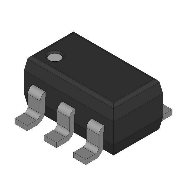
DBV PACKAGE
(TOP VIEW)
Output Swing Includes Both Supply Rails
Low Noise . . . 21 nV/√Hz Typ at f = 1 kHz
Low Input Bias Current . . . 1 pA Typ
Very Low Power . . . 11 µA Per Channel Typ
Common-Mode Input Voltage Range
Includes Negative Rail
Wide Supply Voltage Range
2.7 V to 10 V
Available in the SOT-23 Package
Macromodel Included
IN +
1
VDD− /GND
2
IN −
3
5
VDD+
4
OUT
EQUIVALENT INPUT NOISE VOLTAGE†
vs
FREQUENCY
description
V n − Equivalent Input Noise Voltage − nV/ Hz
80
The TLV2211 is a single low-voltage operational
amplifier available in the SOT-23 package. It
consumes only 11 µA (typ) of supply current and
is ideal for battery-power applications. Looking at
Figure 1, the TLV2211 has a 3-V noise level of
22 nV/√Hz at 1kHz; 5 times lower than competitive
SOT-23 micropower solutions. The device
exhibits rail-to-rail output performance for increased dynamic range in single- or split-supply
applications. The TLV2211 is fully characterized
at 3 V and 5 V and is optimized for low-voltage
applications.
The TLV2211, exhibiting high input impedance
and low noise, is excellent for small-signal
conditioning for high-impedance sources, such as
piezoelectric transducers. Because of the micropower dissipation levels combined with 3-V
operation, these devices work well in hand-held
monitoring and remote-sensing applications. In
addition, the rail-to-rail output feature with single
or split supplies makes this family a great choice
when interfacing with analog-to-digital converters
(ADCs).
VDD = 3 V
RS = 20 Ω
TA = 25°C
70
60
50
40
30
20
10
0
101
102
103
f − Frequency − Hz
104
† All loads are referenced to 1.5 V.
Figure 1. Equivalent Input Noise Voltage
Versus Frequency
AVAILABLE OPTIONS
TA
VIOmax AT 25°C
PACKAGED DEVICES
SOT-23 (DBV)†
SYMBOL
0°C to 70°C
3 mV
TLV2211CDBV
VACC
−40°C to 85°C
3 mV
TLV2211IDBV
VACI
CHIP FORM‡
(Y)
TLV2211Y
† The DBV package available in tape and reel only.
‡ Chip forms are tested at TA = 25°C only.
Please be aware that an important notice concerning availability, standard warranty, and use in critical applications of
Texas Instruments semiconductor products and disclaimers thereto appears at the end of this data sheet.
Advanced LinCMOS is a trademark of Texas Instruments.
Copyright 2001−2006, Texas Instruments Incorporated
���������� ���� ���!"#�$�!� �%
&""��$ �% !� '&()�
�$�!� �$�*
�"! &
$%
!��!"# $! %'�
���
�$�!�% '�" $+� $�"#% !� ��,�% ��%$"&#��$%
%$�� �" -�""��$.* �"! &
$�!� '"!
�%%��/ !�% �!$ ��
�%%�"�). ��
)& �
$�%$��/ !� �)) '�"�#�$�"%*
POST OFFICE BOX 655303
• DALLAS, TEXAS 75265
1
��������� ��������
�
��
� ������� ������������
���������� ������ ����������� ����������
SLOS156E − MAY 1996 − REVISED SEPTEMBER 2006
description (continued)
With a total area of 5.6mm2, the SOT-23 package only requires one-third the board space of the standard 8-pin
SOIC package. This ultra-small package allows designers to place single amplifiers very close to the signal
source, minimizing noise pick-up from long PCB traces. TI has also taken special care to provide a pinout that
is optimized for board layout (see Figure 2). Both inputs are separated by GND to prevent coupling or leakage
paths. The OUT and IN− terminals are on the same end of the board to provide negative feedback. Finally, gain
setting resistors and decoupling capacitor are easily placed around the package.
1
VI
IN +
VDD+
4
V+
C
2
GND
VDD/GND
RI
3
IN −
OUT
5
VO
RF
Figure 2. Typical Surface Mount Layout for a Fixed-Gain Noninverting Amplifier
2
POST OFFICE BOX 655303
• DALLAS, TEXAS 75265
��������� ��������
�
��
� ������� ������������
���������� ������ ����������� ����������
SLOS156E − MAY 1996 − REVISED SEPTEMBER 2006
TLV2211Y chip information
This chip, when properly assembled, displays characteristics similar to the TLV2211C. Thermal compression
or ultrasonic bonding may be used on the doped-aluminum bonding pads. This chip may be mounted with
conductive epoxy or a gold-silicon preform.
BONDING PAD ASSIGNMENTS
(4)
(3)
VDD +
(5)
(1)
+
IN +
(3)
(4)
OUT
−
IN −
(2)
VDD − / GND
40
(2)
CHIP THICKNESS: 10 MILS TYPICAL
BONDING PADS: 4 × 4 MILS MINIMUM
TJmax = 150°C
TOLERANCES ARE ± 10%.
ALL DIMENSIONS ARE IN MILS.
PIN (2) IS INTERNALLY CONNECTED
TO BACK SIDE OF CHIP.
(1)
(5)
32
POST OFFICE BOX 655303
• DALLAS, TEXAS 75265
3
��������� ��������
�
��
� ������� ������������
���������� ������ ����������� ����������
SLOS156E − MAY 1996 − REVISED SEPTEMBER 2006
equivalent schematic
VDD +
Q3
Q6
Q9
R7
Q12
Q14
Q16
C2
IN +
R6
OUT
C1
IN −
R5
Q1
Q4
Q13
Q15
R2
Q2
R3
Q5
Q7
Q8
Q10
Q11
R4
R1
VDD −/ GND
COMPONENT COUNT†
Transistors
Diodes
Resistors
Capacitors
23
6
11
2
† Includes both amplifiers and all
ESD, bias, and trim circuitry
4
POST OFFICE BOX 655303
• DALLAS, TEXAS 75265
D2
Q17
D1
��������� ��������
�
��
� ������� ������������
���������� ������ ����������� ����������
SLOS156E − MAY 1996 − REVISED SEPTEMBER 2006
absolute maximum ratings over operating free-air temperature range (unless otherwise noted)†
Supply voltage, VDD (see Note 1) . . . . . . . . . . . . . . . . . . . . . . . . . . . . . . . . . . . . . . . . . . . . . . . . . . . . . . . . . . . . 12 V
Differential input voltage, VID (see Note 2) . . . . . . . . . . . . . . . . . . . . . . . . . . . . . . . . . . . . . . . . . . . . . . . . . . . ± VDD
Input voltage range, VI (any input, see Note 1) . . . . . . . . . . . . . . . . . . . . . . . . . . . . . . . . . . . . . . . . −0.3 V to VDD
Input current, II (each input) . . . . . . . . . . . . . . . . . . . . . . . . . . . . . . . . . . . . . . . . . . . . . . . . . . . . . . . . . . . . . . . ± 5 mA
Output current, IO . . . . . . . . . . . . . . . . . . . . . . . . . . . . . . . . . . . . . . . . . . . . . . . . . . . . . . . . . . . . . . . . . . . . . . . ± 50 mA
Total current into VDD + . . . . . . . . . . . . . . . . . . . . . . . . . . . . . . . . . . . . . . . . . . . . . . . . . . . . . . . . . . . . . . . . . . ± 50 mA
Total current out of VDD − . . . . . . . . . . . . . . . . . . . . . . . . . . . . . . . . . . . . . . . . . . . . . . . . . . . . . . . . . . . . . . . . ± 50 mA
Duration of short-circuit current (at or below) 25°C (see Note 3) . . . . . . . . . . . . . . . . . . . . . . . . . . . . . . unlimited
Continuous total power dissipation . . . . . . . . . . . . . . . . . . . . . . . . . . . . . . . . . . . . . See Dissipation Rating Table
Operating free-air temperature range, TA: TLV2211C . . . . . . . . . . . . . . . . . . . . . . . . . . . . . . . . . . . 0°C to 70°C
TLV2211I . . . . . . . . . . . . . . . . . . . . . . . . . . . . . . . . . . −40°C to 85°C
Storage temperature range, Tstg . . . . . . . . . . . . . . . . . . . . . . . . . . . . . . . . . . . . . . . . . . . . . . . . . . . −65°C to 150°C
Lead temperature 1,6 mm (1/16 inch) from case for 10 seconds: DBV package . . . . . . . . . . . . . . . . . . 260°C
† Stresses beyond those listed under “absolute maximum ratings” may cause permanent damage to the device. These are stress ratings only, and
functional operation of the device at these or any other conditions beyond those indicated under “recommended operating conditions” is not
implied. Exposure to absolute-maximum-rated conditions for extended periods may affect device reliability.
NOTES: 1. All voltage values, except differential voltages, are with respect to VDD − .
2. Differential voltages are at the noninverting input with respect to the inverting input. Excessive current flows when input is brought
below VDD − − 0.3 V.
3. The output may be shorted to either supply. Temperature and /or supply voltages must be limited to ensure that the maximum
dissipation rating is not exceeded.
DISSIPATION RATING TABLE
PACKAGE
TA ≤ 25°C
25 C
POWER RATING
DERATING FACTOR
ABOVE TA = 25°C
70°C
TA = 70
C
POWER RATING
85°C
TA = 85
C
POWER RATING
DBV
150 mW
1.2 mW/°C
96 mW
78 mW
recommended operating conditions
TLV2211C
MIN
Supply voltage, VDD ���� ���� ��
2.7
Input voltage range, VI
VDD −
VDD −
Common-mode input voltage, VIC
Operating free-air temperature, TA
NOTE 1: All voltage values, except differential voltages, are with respect to VDD − .
POST OFFICE BOX 655303
0
• DALLAS, TEXAS 75265
MAX
10
VDD + − 1.3
VDD + − 1.3
70
TLV2211I
MIN
2.7
VDD −
VDD −
−40
MAX
10
VDD + − 1.3
VDD + − 1.3
85
UNIT
V
V
V
°C
5
��������� ��������
�
��
� ������� ������������
���������� ������ ����������� ����������
SLOS156E − MAY 1996 − REVISED SEPTEMBER 2006
electrical characteristics at specified free-air temperature, VDD = 3 V (unless otherwise noted)
PARAMETER
VIO
Input offset voltage
αVIO
Temperature
coefficient of input
offset voltage
Input offset voltage
long-term drift
(see Note 4)
IIO
IIB
VICR
VOH
VOL
AVD
TA†
TEST CONDITIONS
TLV2211C
MIN
Full range
VDD ± = ± 1.5 V,
VO = 0,
VIC = 0,
RS = 50 Ω
25°C
TLV2211I
TYP
MAX
0.47
3
MIN
TYP
MAX
0.47
3
UNIT
mV
1
1
µV/°C
V/°C
0.003
0.003
µV/mo
Input offset current
Full range
0.5
60
0.5
60
pA
Input bias current
Full range
1
60
1
60
pA
Common-mode input
voltage range
High-level output
voltage
Low-level output
voltage
Large-signal
differential voltage
amplification
|VIO | ≤ 5 mV,
25°C
25
C
0
to
2
Full range
0
to
1.7
RS = 50 Ω
IOH = − 100 µA
A
IOH = − 250 µA
−0.3
to
2.2
0
to
2
−0.3
to
2.2
V
0
to
1.7
25°C
2.94
2.94
25°C
2.85
2.85
Full range
2.5
V
2.5
VIC = 1.5 V,
IOL = 50 µA
25°C
15
IOL = 500 µA
A
25°C
150
VIC = 1.5 V,
Full range
RL = 10 kه
25°C
3
VIC = 1.5 V,
VO = 1 V to 2 V
Full range
1
RL = 1 Mه
25°C
600
600
15
150
500
7
mV
500
3
7
1
V/mV
ri(d)
Differential input
resistance
25°C
1012
1012
Ω
ri(c)
Common-mode
input resistance
25°C
1012
1012
Ω
ci(c)
Common-mode
input capacitance
f = 10 kHz,
25°C
5
5
pF
zo
Closed-loop
output impedance
f = 7 kHz,
AV = 1
25°C
200
200
Ω
CMRR
Common-mode
rejection ratio
VIC = 0 to 1.7 V,
RS = 50 Ω
VO = 1.5 V,
kSVR
Supply voltage
rejection ratio
(∆VDD /∆VIO)
VDD = 2.7 V to 8 V,
No load
VIC = VDD /2
,
IDD
Supply current
VO = 1.5 V,
No load
25°C
65
Full range
60
25°C
80
Full range
80
83
65
83
dB
60
95
80
95
dB
25°C
Full range
80
11
25
30
11
25
30
µA
† Full range for the TLV2211C is 0°C to 70°C. Full range for the TLV2211I is − 40°C to 85°C.
‡ Referenced to 1.5 V
NOTE 4: Typical values are based on the input offset voltage shift observed through 500 hours of operating life test at TA = 150°C extrapolated
to TA = 25°C using the Arrhenius equation and assuming an activation energy of 0.96 eV.
6
POST OFFICE BOX 655303
• DALLAS, TEXAS 75265
��������� ��������
�
��
� ������� ������������
���������� ������ ����������� ����������
SLOS156E − MAY 1996 − REVISED SEPTEMBER 2006
operating characteristics at specified free-air temperature, VDD = 3 V (unless otherwise noted)
PARAMETER
SR
Slew rate at unity gain
Vn
Equivalent input noise
voltage
VN(PP)
Peak-to-peak equivalent
input noise voltage
In
Equivalent input noise
current
TEST CONDITIONS
VO = 1.1 V to 1.9 V,
CL = 100 pF‡
RL = 10 kه,
TLV2211C
TA†
MIN
25°C
0.01 0.025
Full
range
TYP
0.005
TLV2211I
MAX
MIN
TYP
MAX
UNIT
0.01 0.025
V/µs
0.005
f = 10 Hz
25°C
80
80
f = 1 kHz
25°C
22
22
f = 0.1 Hz to 1 Hz
25°C
660
660
f = 0.1 Hz to 10 Hz
25°C
880
880
25°C
0.6
0.6
fA /√Hz
25°C
56
56
kHz
25°C
7
7
kHz
25°C
56°
56°
25°C
20
20
Gain-bandwidth product
f = 10 kHz,
CL = 100 pF‡
RL = 10 kه,
BOM
Maximum output-swing
bandwidth
VO(PP) = 1 V,
RL = 10 kه,
AV = 1,
CL = 100 pF‡
φm
Phase margin at
unity gain
RL = 10 kه,
CL = 100 pF‡
Gain margin
† Full range is − 40°C to 85°C.
‡ Referenced to 1.5 V
POST OFFICE BOX 655303
• DALLAS, TEXAS 75265
nV/√Hz
nV
dB
7
��������� ��������
�
��
� ������� ������������
���������� ������ ����������� ����������
SLOS156E − MAY 1996 − REVISED SEPTEMBER 2006
electrical characteristics at specified free-air temperature, VDD = 5 V (unless otherwise noted)
PARAMETER
VIO
Input offset voltage
αVIO
Temperature
coefficient of input
offset voltage
Input offset voltage
long-term drift
(see Note 5)
IIO
Input offset current
IIB
Input bias current
VICR
VOH
VOL
AVD
Common-mode input
voltage range
High-level output
voltage
Low-level output
voltage
Large-signal
differential
voltage amplification
TA†
TEST CONDITIONS
TLV2211C
MIN
Full range
VDD ± = ± 2.5 V,
VO = 0,
VIC = 0,
RS = 50 Ω
MAX
0.45
3
µV/mo
25°C
0.5
VIC = 2.5 V,
VO = 1 V to 4 V
RL = 10 kه
RL = 1 Mه
60
0.5
150
1
25°C
25
C
0
to
4
60
Full range
0
to
3.5
−0.3
to
4.2
1
0
to
4
−0.3
to
4.2
V
4.875
V
4.5
25°C
12
25°C
120
Full range
12
120
500
3
pA
4.95
4.875
Full range
pA
0
to
3.5
4.5
6
60
150
4.95
25°C
60
150
150
25°C
IOL = 500 µA
mV
0.003
Full range
VIC = 2.5 V,
3
0.003
25°C
IOL = 50 µA
0.45
UNIT
25°C
RS = 50 Ω
VIC = 2.5 V,
MAX
µV/°C
Full range
IOH = − 250 µA
TYP
0.5
25°C
IOH = − 100 µA
MIN
0.5
Full range
|VIO | ≤ 5 mV
TLV2211I
TYP
12
mV
500
6
12
3
V/mV
25°C
800
800
ri(d)
Differential input
resistance
25°C
1012
1012
Ω
ri(c)
Common-mode
input resistance
25°C
1012
1012
Ω
ci(c)
Common-mode
input capacitance
f = 10 kHz,
25°C
5
5
pF
zo
Closed-loop
output impedance
f = 7 kHz,
AV = 1
25°C
200
200
Ω
CMRR
Common-mode
rejection ratio
VIC = 0 to 2.7 V,
RS = 50 Ω
VO = 2.5 V,
kSVR
Supply voltage
rejection ratio
(∆VDD /∆VIO)
VDD = 4.4 V to 8 V,
No load
VIC = VDD /2,
IDD
Supply current
VO = 2.5 V,
No load
25°C
70
Full range
70
25°C
80
Full range
80
83
70
83
dB
70
95
80
95
dB
25°C
Full range
80
13
25
30
13
25
30
µA
† Full range for the TLV2211C is 0°C to 70°C. Full range for the TLV2211I is − 40°C to 85°C.
‡ Referenced to 1.5 V
NOTE 5: Typical values are based on the input offset voltage shift observed through 500 hours of operating life test at TA = 150°C extrapolated
to TA = 25°C using the Arrhenius equation and assuming an activation energy of 0.96 eV.
8
POST OFFICE BOX 655303
• DALLAS, TEXAS 75265
��������� ��������
�
��
� ������� ������������
���������� ������ ����������� ����������
SLOS156E − MAY 1996 − REVISED SEPTEMBER 2006
operating characteristics at specified free-air temperature, VDD = 5 V (unless otherwise noted)
PARAMETER
SR
Slew rate at unity gain
Vn
Equivalent input noise
voltage
VN(PP)
Peak-to-peak equivalent
input noise voltage
In
Equivalent input noise
current
TEST CONDITIONS
VO = 1.5 V to 3.5 V,
CL = 100 pF‡
RL = 10 kه,
TLV2211C
TA†
MIN
25°C
0.01 0.025
Full
range
TYP
TLV2211I
MAX
0.005
MIN
TYP
MAX
UNIT
0.01 0.025
V/µs
0.005
f = 10 Hz
25°C
72
72
f = 1 kHz
25°C
21
21
f = 0.1 Hz to 1 Hz
25°C
600
600
f = 0.1 Hz to 10 Hz
25°C
800
800
25°C
0.6
0.6
fA /√Hz
25°C
65
65
kHz
25°C
7
7
kHz
25°C
56°
56°
25°C
22
22
Gain-bandwidth product
f = 10 kHz,
CL = 100 pF‡
RL = 10 kه,
BOM
Maximum output-swing
bandwidth
VO(PP) = 2 V,
RL = 10 kه,
AV = 1,
CL = 100 pF‡
φm
Phase margin at
unity gain
RL = 10 kه,
CL = 100 pF‡
Gain margin
† Full range is − 40°C to 85°C.
‡ Referenced to 1.5 V
nV/√Hz
nV
dB
electrical characteristics at VDD = 3 V, TA = 25°C (unless otherwise noted)
PARAMETER
VIO
IIO
Input offset voltage
IIB
Input bias current
Input offset current
TLV2211Y
TEST CONDITIONS
VDD ± = ± 1.5 V,
RS = 50 Ω
MIN
TYP
MAX
0.47
VO = 0,
VIC = 0,
mV
0.5
60
pA
1
60
pA
−0.3
to 2.2
VICR
Common-mode input voltage range
| VIO | ≤ 5 mV,
VOH
High-level output voltage
IOH = −100 µA
IOH = − 200 µA
VOL
Low-level output voltage
VIC = 0,
VIC = 0,
IOL = 50 µA
IOL = 500 µA
AVD
Large-signal differential
voltage amplification
VIC = 1.5 V,
VO = 1 V to 2 V
ri(d)
Differential input resistance
ri(c)
Common-mode input resistance
ci(c)
Common-mode input capacitance
f = 10 kHz
zo
Closed-loop output impedance
f = 7 kHz,
Ω
Common-mode rejection ratio
VIC = 0 to 1.7 V,
AV = 1
VO = 1.5 V,
200
CMRR
RS = 50 Ω
83
dB
kSVR
Supply voltage rejection ratio
(∆VDD /∆VIO)
VDD = 2.7 V to 8 V,
VIC = VDD/2,
No load
95
dB
VO = 1.5 V,
No load
11
µA
IDD
Supply current
† Referenced to 1.5 V
POST OFFICE BOX 655303
RS = 50 Ω
UNIT
V
2.94
2.85
• DALLAS, TEXAS 75265
V
15
150
RL = 10 kن
7
RL = 1 Mن
600
mV
V/mV
1012
1012
Ω
5
pF
Ω
9
��������� ��������
�
��
� ������� ������������
���������� ������ ����������� ����������
SLOS156E − MAY 1996 − REVISED SEPTEMBER 2006
electrical characteristics at VDD = 5 V, TA = 25°C (unless otherwise noted)
PARAMETER
VIO
IIO
Input offset voltage
IIB
Input bias current
VICR
Common-mode input voltage range
VOH
High-level output voltage
VOL
Low-level output voltage
AVD
Large-signal differential
voltage amplification
ri(d)
Differential input resistance
ri(c)
Common-mode input resistance
ci(c)
Common-mode input capacitance
f = 10 kHz
zo
Closed-loop output impedance
f = 7 kHz,
CMRR
Common-mode rejection ratio
kSVR
Supply voltage rejection ratio
(∆VDD /∆VIO)
Input offset current
IDD
Supply current
† Referenced to 1.5 V
10
TLV2211Y
TEST CONDITIONS
TYP
MAX
0.45
VDD ± = ± 2.5 V,
RS = 50 Ω
VIC = 0,
| VIO | ≤ 5 mV,
RS = 50 Ω
IOH = − 100 µA
IOH = − 250 µA
VIC = 2.5 V,
MIN
VO = 0,
UNIT
mV
0.5
60
pA
1
60
pA
−0.3
to 4.2
V
4.95
4.875
VIC = 2.5 V,
IOL = 50 µA
IOL = 500 µA
VIC = 2.5 V,
VO = 1 V to 4 V
V
12
120
RL = 10 kن
12
RL = 1 Mن
800
mV
V/mV
1012
1012
Ω
5
pF
200
Ω
Ω
VIC = 0 to 2.7 V,
AV = 1
VO = 2.5 V,
RS = 50 Ω
83
dB
VDD = 4.4 V to 8 V,
VIC = VDD/2,
No load
95
dB
VO = 2.5 V,
No load
13
µA
POST OFFICE BOX 655303
• DALLAS, TEXAS 75265
��������� ��������
�
��
� ������� ������������
���������� ������ ����������� ����������
SLOS156E − MAY 1996 − REVISED SEPTEMBER 2006
TYPICAL CHARACTERISTICS
Table of Graphs
FIGURE
VIO
Input offset voltage
Distribution
vs Common-mode input voltage
3, 4
5, 6
αVIO
IIB/IIO
Input offset voltage temperature coefficient
Distribution
7, 8
Input bias and input offset currents
vs Free-air temperature
9
VI
Input voltage
vs Supply voltage
vs Free-air temperature
10
11
VOH
VOL
High-level output voltage
vs High-level output current
12, 15
Low-level output voltage
vs Low-level output current
13, 14, 16
VO(PP)
Maximum peak-to-peak output voltage
vs Frequency
17
IOS
Short-circuit output current
vs Supply voltage
vs Free-air temperature
18
19
VO
Output voltage
vs Differential input voltage
20, 21
AVD
Differential voltage amplification
vs Load resistance
vs Frequency
vs Free-air temperature
22
23, 24
25, 26
zo
Output impedance
vs Frequency
27, 28
CMRR
Common-mode rejection ratio
vs Frequency
vs Free-air temperature
29
30
kSVR
Supply-voltage rejection ratio
vs Frequency
vs Free-air temperature
31, 32
33
IDD
Supply current
vs Supply voltage
34
SR
Slew rate
vs Load capacitance
vs Free-air temperature
35
36
VO
VO
Large-signal pulse response
vs Time
37, 38, 39, 40
Small-signal pulse response
vs Time
41, 42, 43, 44
Vn
Equivalent input noise voltage
vs Frequency
Noise voltage (referred to input)
Over a 10-second period
47
Total harmonic distortion plus noise
vs Frequency
48
Gain-bandwidth product
vs Free-air temperature
vs Supply voltage
49
50
Phase margin
vs Frequency
vs Load capacitance
23, 24
51
Gain margin
vs Load capacitance
52
Unity-gain bandwidth
vs Load capacitance
53
THD + N
φm
B1
POST OFFICE BOX 655303
• DALLAS, TEXAS 75265
45, 46
11
��������� ��������
�
��
� ������� ������������
���������� ������ ����������� ����������
SLOS156E − MAY 1996 − REVISED SEPTEMBER 2006
TYPICAL CHARACTERISTICS
DISTRIBUTION OF TLV2211
INPUT OFFSET VOLTAGE
DISTRIBUTION OF TLV2211
INPUT OFFSET VOLTAGE
30
30
376 Amplifiers From 1 Wafer Lot
VDD = ± 1.5 V
TA = 25°C
25
Precentage of Amplifiers − %
Precentage of Amplifiers − %
25
20
15
10
5
0
376 Amplifiers From 1 Wafer Lot
VDD = ± 2.5 V
TA = 25°C
20
15
10
5
−1.5
−1
−0.5
0
0.5
1
VIO − Input Offset Voltage − mV
0
1.5
−1.5
−1
−0.5
0
0.5
1
VIO − Input Offset Voltage − mV
Figure 3
Figure 4
INPUT OFFSET VOLTAGE†
vs
COMMON-MODE INPUT VOLTAGE
INPUT OFFSET VOLTAGE†
vs
COMMON-MODE INPUT VOLTAGE
1
ÁÁ
ÁÁ
1
VDD = 3 V
RS = 50 Ω
TA = 25°C
0.8
0.6
VIO − Input Offset Voltage − mV
VIO − Input Offset Voltage − mV
0.8
0.4
0.2
0
−0.2
ÁÁ
ÁÁ
ÁÁ
−0.4
−0.6
−0.8
−1
−1
0
1
2
3
VIC − Common-Mode Input Voltage − V
VDD = 5 V
RS = 50 Ω
TA = 25°C
0.6
0.4
0.2
0
−0.2
−0.4
−0.6
−0.8
−1
−1
0
1
2
3
4
VIC − Common-Mode Input Voltage − V
Figure 6
Figure 5
† For all curves where VDD = 5 V, all loads are referenced to 2.5 V. For all curves where VDD = 3 V, all loads are referenced to 1.5 V.
12
1.5
POST OFFICE BOX 655303
• DALLAS, TEXAS 75265
5
��������� ��������
�
��
� ������� ������������
���������� ������ ����������� ����������
SLOS156E − MAY 1996 − REVISED SEPTEMBER 2006
TYPICAL CHARACTERISTICS
DISTRIBUTION OF TLV2211 INPUT OFFSET
VOLTAGE TEMPERATURE COEFFICIENT
DISTRIBUTION OF TLV2211 INPUT OFFSET
VOLTAGE TEMPERATURE COEFFICIENT
50
32 Amplifiers From 1 Wafer Lot
VDD = ± 1.5 V
P Package
TA = 25°C
40
Percentage of Amplifiers − %
Percentage of Amplifiers − %
50
30
20
10
0
−3
−2
−1
0
1
2
32 Amplifiers From 1 Wafer Lot
VDD = ± 2.5 V
P Package
TA = 25°C
40
30
20
10
0
3
−3
α VIO − Temperature Coefficient − µ V / °C
−2
−1
5
VDD± = ± 2.5 V
VIC = 0
VO = 0
RS = 50 Ω
RS = 50 Ω
TA = 25°C
4
3
70
VI − Input Voltage − V
IIIB
IB and IIIO
IO − Input Bias and Input Offset Currents − pA
3
INPUT VOLTAGE
vs
SUPPLY VOLTAGE
100
60
50
40
IIB
20
2
1
0
| VIO | ≤ 5 mV
−1
ÁÁ
ÁÁ
30
−2
−3
IIO
−4
10
0
25
2
Figure 8
INPUT BIAS AND INPUT OFFSET CURRENTS†
vs
FREE-AIR TEMPERATURE
80
1
α VIO − Temperature Coefficient − µ V / °C
Figure 7
90
0
−5
45
65
85
105
TA − Free-Air Temperature − °C
125
1
Figure 9
1.5
2
2.5
3
3.5
| VDD ± | − Supply Voltage − V
4
Figure 10
† Data at high and low temperatures are applicable only within the rated operating free-air temperature ranges of the various devices.
POST OFFICE BOX 655303
• DALLAS, TEXAS 75265
13
��������� ��������
�
��
� ������� ������������
���������� ������ ����������� ����������
SLOS156E − MAY 1996 − REVISED SEPTEMBER 2006
TYPICAL CHARACTERISTICS
INPUT VOLTAGE†‡
vs
FREE-AIR TEMPERATURE
HIGH-LEVEL OUTPUT VOLTAGE†‡
vs
HIGH-LEVEL OUTPUT CURRENT
5
3
VDD = 5 V
VDD = 3 V
VOH − High-Level Output Voltage − V
VI − Input Voltage − V
4
3
| VIO | ≤ 5 mV
2
ÁÁÁ
1
0
−1
−55 −35 −15
5
25
45
65 85 105
TA − Free-Air Temperature − °C
125
ÁÁ
ÁÁ
ÁÁ
2.5
TA = − 40°C
2
TA = 25°C
1.5
TA = 85°C
1
TA = 125°C
0.5
0
0
200
1.4
1
VIC = 0
VOL − Low-Level Output Voltage − V
VOL − Low-Level Output Voltage − V
LOW-LEVEL OUTPUT VOLTAGE†‡
vs
LOW-LEVEL OUTPUT CURRENT
VDD = 3 V
TA = 25°C
VIC = 0.75 V
0.8
0.6
VIC = 1.5 V
ÁÁ
ÁÁ
ÁÁ
0.4
0.2
0
0
1
2
3
4
5
VDD = 3 V
VIC = 1.5 V
1.2
TA = 125°C
1
TA = 85°C
0.8
TA = 25°C
0.6
0.4
TA = − 40°C
0.2
0
0
IOL − Low-Level Output Current − mA
Figure 13
1
2
3
4
IOL − Low-Level Output Current − mA
Figure 14
† Data at high and low temperatures are applicable only within the rated operating free-air temperature ranges of the various devices.
‡ For all curves where VDD = 5 V, all loads are referenced to 2.5 V. For all curves where VDD = 3 V, all loads are referenced to 1.5 V.
14
800
Figure 12
LOW-LEVEL OUTPUT VOLTAGE‡
vs
LOW-LEVEL OUTPUT CURRENT
ÁÁ
ÁÁ
600
| IOH | − High-Level Output Current − µ A
Figure 11
1.2
400
POST OFFICE BOX 655303
• DALLAS, TEXAS 75265
5
��������� ��������
�
��
� ������� ������������
���������� ������ ����������� ����������
SLOS156E − MAY 1996 − REVISED SEPTEMBER 2006
TYPICAL CHARACTERISTICS
LOW-LEVEL OUTPUT VOLTAGE†‡
vs
LOW-LEVEL OUTPUT CURRENT
HIGH-LEVEL OUTPUT VOLTAGE†‡
vs
HIGH-LEVEL OUTPUT CURRENT
1.4
5
VDD = 5 V
VIC = 2.5 V
ÁÁ
ÁÁ
1.2
4
VOL − Low-Level Output Voltage − V
VOH − High-Level Output Voltage − V
TA = 125°C
TA = 85°C
TA = 25°C
3
TA = − 40°C
2
VDD = 5 V
VIC = 2.5 V
0
200
TA = 85°C
0.8
TA = 25°C
0.6
0.4
ÁÁ
ÁÁ
1
0
TA = 125°C
1
400
600
800
TA = − 40°C
0.2
0
0
1000
1
| IOH | − High-Level Output Current − µA
Figure 15
4
5
6
SHORT-CIRCUIT OUTPUT CURRENT
vs
SUPPLY VOLTAGE
16
5
VDD = 5 V
I OS − Short-Circuit Output Current − mA
VO(PP) − Maximum Peak-to-Peak Output Voltage − V
3
Figure 16
MAXIMUM PEAK-TO-PEAK OUTPUT VOLTAGE‡
vs
FREQUENCY
ÁÁ
ÁÁ
ÁÁ
2
IOL − Low-Level Output Current − mA
4
3
VDD = 3 V
2
1
RI = 10 kΩ
TA = 25°C
0
102
12
104
VID = − 100 mV
10
8
6
4
2
VID = 100 mV
0
−2
103
f − Frequency − Hz
VO = VDD/2
VIC = VDD/2
TA = 25°C
14
2
3
4
5
6
VDD − Supply Voltage − V
7
8
Figure 18
Figure 17
† Data at high and low temperatures are applicable only within the rated operating free-air temperature ranges of the various devices.
‡ For all curves where VDD = 5 V, all loads are referenced to 2.5 V. For all curves where VDD = 3 V, all loads are referenced to 1.5 V.
POST OFFICE BOX 655303
• DALLAS, TEXAS 75265
15
��������� ��������
�
��
� ������� ������������
���������� ������ ����������� ����������
SLOS156E − MAY 1996 − REVISED SEPTEMBER 2006
TYPICAL CHARACTERISTICS
SHORT-CIRCUIT OUTPUT CURRENT†‡
vs
FREE-AIR TEMPERATURE
OUTPUT VOLTAGE‡
vs
DIFFERENTIAL INPUT VOLTAGE
3
VDD = 5 V
VIC = 2.5 V
VO = 2.5 V
12
10
VID = − 100 mV
8
6
4
2
−2
−75
−50
2
1.5
1
0.5
VID = 100 mV
0
VDD = 3 V
RI = 10 kΩ
VIC = 1.5 V
TA = 25°C
2.5
V O − Output Voltage − V
I OS − Short-Circuit Output Current − mA
14
−25
0
25
50
75
100
TA − Free-Air Temperature − °C
0
−1000 −750 −500 −250 0
250 500 750 1000
VID − Differential Input Voltage − µV
125
Figure 19
Figure 20
OUTPUT VOLTAGE‡
vs
DIFFERENTIAL INPUT VOLTAGE
VDD = 5 V
VIC = 2.5 V
RL = 10 kΩ
TA = 25°C
V O − Output Voltage − V
4
3
2
1
0
−1000 −750 −500 −250 0
250 500 750 1000
VID − Differential Input Voltage − µV
AVD − Differential Voltage Amplification − V/mV
5
DIFFERENTIAL VOLTAGE AMPLIFICATION‡
vs
LOAD RESISTANCE
103
VO(PP) = 2 V
TA = 25°C
VDD = 5 V
102
VDD = 3 V
101
ÁÁ
ÁÁ
1
0.1
1
101
102
RL − Load Resistance − kΩ
Figure 21
Figure 22
† Data at high and low temperatures are applicable only within the rated operating free-air temperature ranges of the various devices.
‡ For all curves where VDD = 5 V, all loads are referenced to 2.5 V. For all curves where VDD = 3 V, all loads are referenced to 1.5 V.
16
POST OFFICE BOX 655303
• DALLAS, TEXAS 75265
103
��������� ��������
�
��
� ������� ������������
���������� ������ ����������� ����������
SLOS156E − MAY 1996 − REVISED SEPTEMBER 2006
TYPICAL CHARACTERISTICS
LARGE-SIGNAL DIFFERENTIAL VOLTAGE
AMPLIFICATION AND PHASE MARGIN†
vs
FREQUENCY
40
20
45°
Phase Margin
10
0°
0
Gain
−10
−20
φom
m − Phase Margin
AVD
A
VD − Large-Signal Differential
Voltage Amplification − dB
30
ÁÁ
ÁÁ
90°
VDD = 3 V
RL = 10 kΩ
CL= 100 pF
TA = 25°C
−45°
−30
−40
103
104
105
f − Frequency − Hz
−90°
106
Figure 23
LARGE-SIGNAL DIFFERENTIAL VOLTAGE
AMPLIFICATION AND PHASE MARGIN†
vs
FREQUENCY
40
20
45°
Phase Margin
10
0°
0
Gain
−10
−20
φom
m − Phase Margin
AVD
A
VD − Large-Signal Differential
Voltage Amplification − dB
30
ÁÁ
ÁÁ
90°
VDD = 5 V
RL= 10 kΩ
CL= 100 pF
TA = 25°C
−45°
−30
−40
103
104
105
f − Frequency − Hz
−90°
106
Figure 24
† For all curves where VDD = 5 V, all loads are referenced to 2.5 V. For all curves where VDD = 3 V, all loads are referenced to 1.5 V.
POST OFFICE BOX 655303
• DALLAS, TEXAS 75265
17
��������� ��������
�
��
� ������� ������������
���������� ������ ����������� ����������
SLOS156E − MAY 1996 − REVISED SEPTEMBER 2006
TYPICAL CHARACTERISTICS
LARGE-SIGNAL DIFFERENTIAL
VOLTAGE AMPLIFICATION†‡
vs
FREE-AIR TEMPERATURE
LARGE-SIGNAL DIFFERENTIAL
VOLTAGE AMPLIFICATION†‡
vs
FREE-AIR TEMPERATURE
104
10 3
AVD − Large-Signal Differential Voltage
Amplification − V/mV
AVD − Large-Signal Differential Voltage
Amplification − V/mV
RL = 1 MΩ
10 2
10 1
RL = 10 kΩ
VDD = 3 V
VIC = 1.5 V
VO = 0.5 V to 2.5 V
1
−75
−50
−25
0
25
50
75
100
TA − Free-Air Temperature − °C
VDD = 5 V
VIC = 2.5 V
VO = 1 V to 4 V
103
RL = 1 MΩ
102
101
RL = 10 kΩ
1
−75
125
−50
−25
0
25
50
75 100
TA − Free-Air Temperature − °C
Figure 25
Figure 26
OUTPUT IMPEDANCE‡
vs
FREQUENCY
OUTPUT IMPEDANCE‡
vs
FREQUENCY
10 3
10 3
VDD = 5 V
TA = 25°C
z o − Output Impedance − Ω
z o − Output Impedance − Ω
VDD = 3 V
TA = 25°C
10 2
AV = 100
AV = 10
101
AV = 100
10 2
101
AV = 10
AV = 1
1
10 1
AV = 1
10 2
10 3
f− Frequency − Hz
10 4
1
101
Figure 27
102
103
f− Frequency − Hz
Figure 28
† Data at high and low temperatures are applicable only within the rated operating free-air temperature ranges of the various devices.
‡ For all curves where VDD = 5 V, all loads are referenced to 2.5 V. For all curves where VDD = 3 V, all loads are referenced to 1.5 V.
18
125
POST OFFICE BOX 655303
• DALLAS, TEXAS 75265
104
��������� ��������
�
��
� ������� ������������
���������� ������ ����������� ����������
SLOS156E − MAY 1996 − REVISED SEPTEMBER 2006
TYPICAL CHARACTERISTICS
COMMON-MODE REJECTION RATIO†
vs
FREQUENCY
COMMON-MODE REJECTION RATIO†‡
vs
FREE-AIR TEMPERATURE
88
TA = 25°C
VDD = 5 V
VO = 2.5 V
80
60 VDD = 3 V
VO = 1.5 V
40
20
0
10 1
10 2
10 3
f − Frequency − Hz
10 4
CMMR − Common-Mode Rejection Ratio − dB
CMRR − Common-Mode Rejection Ratio − dB
100
86
VDD = 5 V
84
VDD = 3 V
82
80
78
0
25
50
75 100
− 75 − 50 − 25
TA − Free-Air Temperature − °C
10 5
Figure 29
Figure 30
SUPPLY-VOLTAGE REJECTION RATIO†
vs
FREQUENCY
SUPPLY-VOLTAGE REJECTION RATIO†
vs
FREQUENCY
100
VDD = 3 V
TA = 25°C
80
k SVR − Supply-Voltage Rejection Ratio − dB
k SVR − Supply-Voltage Rejection Ratio − dB
100
kSVR +
60
40
kSVR −
20
ÁÁ
ÁÁ
0
−20
10 1
125
10 2
10 3
10 4
f − Frequency − Hz
10 5
10 6
VDD = 5 V
TA = 25°C
kSVR +
80
60
kSVR −
40
20
ÁÁ
ÁÁ
ÁÁ
0
−20
101
Figure 31
10 2
10 3
10 4
10 5
10 6
f − Frequency − Hz
Figure 32
† For all curves where VDD = 5 V, all loads are referenced to 2.5 V. For all curves where VDD = 3 V, all loads are referenced to 1.5 V.
‡ Data at high and low temperatures are applicable only within the rated operating free-air temperature ranges of the various devices.
POST OFFICE BOX 655303
• DALLAS, TEXAS 75265
19
��������� ��������
�
��
� ������� ������������
���������� ������ ����������� ����������
SLOS156E − MAY 1996 − REVISED SEPTEMBER 2006
TYPICAL CHARACTERISTICS
SUPPLY-VOLTAGE REJECTION RATIO†
vs
FREE-AIR TEMPERATURE
SUPPLY CURRENT†
vs
SUPPLY VOLTAGE
30
VDD = 2.7 V to 8 V
VIC = VO = VDD / 2
96
20
TA = − 40°C
TA = 25°C
15
ÁÁ
ÁÁ
ÁÁ
94
Á
Á
Á
VO = VDD/2
VIC = VDD/2
No Load
25
98
I DD − Supply Current − µ A
k SVR − Supply-Voltage Rejection Ratio − dB
100
92
90
−75 −50
−25
0
25
50
75
100
10
TA = 85°C
5
0
125
0
2
TA − Free-Air Temperature − °C
Figure 33
8
10
SLEW RATE†‡
vs
FREE-AIR TEMPERATURE
0.050
0.040
VDD = 5 V
AV = − 1
TA = 25°C
SR −
0.040
0.030
SR − Slew Rate − V/ µ s
SR − Slew Rate − V/ µ s
6
Figure 34
SLEW RATE‡
vs
LOAD CAPACITANCE
0.035
4
VDD − Supply Voltage − V
0.025
SR +
0.020
0.015
VDD = 5 V
RL = 10 kΩ
CL = 100 pF
AV = 1
SR −
0.030
SR +
0.020
0.010
0.010
0.05
0
101
102
103
104
CL − Load Capacitance − pF
105
0
−75
−50
Figure 35
−25
0
25
50
75 100
TA − Free-Air Temperature − °C
Figure 36
† Data at high and low temperatures are applicable only within the rated operating free-air temperature ranges of the various devices.
‡ For all curves where VDD = 5 V, all loads are referenced to 2.5 V. For all curves where VDD = 3 V, all loads are referenced to 1.5 V.
20
POST OFFICE BOX 655303
• DALLAS, TEXAS 75265
125
��������� ��������
�
��
� ������� ������������
���������� ������ ����������� ����������
SLOS156E − MAY 1996 − REVISED SEPTEMBER 2006
TYPICAL CHARACTERISTICS
INVERTING LARGE-SIGNAL PULSE
RESPONSE†
INVERTING LARGE-SIGNAL PULSE
RESPONSE†
3
5
VO − Output Voltage − V
2.5
2
1.5
1
3
2
1
0.5
0
VDD = 5 V
RL = 10 kΩ
CL = 100 pF
AV = − 1
TA = 25°C
4
VO − Output Voltage − V
VDD = 3 V
RL = 10 kΩ
CL = 100 pF
AV = −1
TA = 25°C
0
0
50 100 150 200 250 300 350 400 450 500
t − Time − µs
0
50 100 150 200 250 300 350 400 450 500
t − Time − µs
Figure 37
Figure 38
VOLTAGE-FOLLOWER LARGE-SIGNAL
PULSE RESPONSE†
VOLTAGE-FOLLOWER LARGE-SIGNAL
PULSE RESPONSE†
5
VDD = 5 V
RL = 10 kΩ
CL = 100 pF
4 A =1
V
TA = 25°C
VDD = 5 V
CL = 100 pF
AV = 1
TA = 25°C
4
VO − Output Voltage − V
VO − Output Voltage − V
5
3
2
1
3
2
RL = 10 kΩ
Tied to 2.5 V
1
0
0
100 200 300 400 500 600 700 800 900 1000
t − Time − µs
RL = 100 kΩ
Tied to 2.5 V
RL = 10 kΩ
Tied to 0 V
0
0
100
200
300
400
500
t − Time − µs
Figure 39
Figure 40
† For all curves where VDD = 5 V, all loads are referenced to 2.5 V. For all curves where VDD = 3 V, all loads are referenced to 1.5 V.
POST OFFICE BOX 655303
• DALLAS, TEXAS 75265
21
��������� ��������
�
��
� ������� ������������
���������� ������ ����������� ����������
SLOS156E − MAY 1996 − REVISED SEPTEMBER 2006
TYPICAL CHARACTERISTICS
INVERTING SMALL-SIGNAL
PULSE RESPONSE†
INVERTING SMALL-SIGNAL
PULSE RESPONSE†
0.76
2.58
VDD = 3 V
RL = 10 kΩ
CL = 100 pF
AV = − 1
TA = 25°C
2.56
VO
VO − Output Voltage − V
VO − Output Voltage − V
074
VDD = 5 V
RL = 10 kΩ
CL = 100 pF
AV = − 1
TA = 25°C
0.72
0.7
0.68
0.66
2.54
2.52
2.5
2.48
2.46
0.64
0
10
20
30
40
2.44
50
0
10
20
30
t − Time − µs
t − Time − µs
Figure 41
VOLTAGE-FOLLOWER SMALL-SIGNAL
PULSE RESPONSE†
0.76
2.58
VDD = 3 V
RL = 10 kΩ
CL = 100 pF
AV = 1
TA = 25°C
VDD = 5 V
RL = 10 kΩ
CL = 100 pF
AV = 1
TA = 25°C
2.56
VO
VO − Output Voltage − V
VO
VO − Output Voltage − V
0.74
0.72
0.7
0.68
0.66
2.54
2.52
2.5
2.48
2.46
0
10
20
30
40
50
2.44
0
t − Time − µs
10
20
30
40
t − Time − µs
Figure 44
Figure 43
† For all curves where VDD = 5 V, all loads are referenced to 2.5 V. For all curves where VDD = 3 V, all loads are referenced to 1.5 V.
22
50
Figure 42
VOLTAGE-FOLLOWER SMALL-SIGNAL
PULSE RESPONSE†
0.64
40
POST OFFICE BOX 655303
• DALLAS, TEXAS 75265
50
��������� ��������
�
��
� ������� ������������
���������� ������ ����������� ����������
SLOS156E − MAY 1996 − REVISED SEPTEMBER 2006
TYPICAL CHARACTERISTICS
EQUIVALENT INPUT NOISE VOLTAGE†
vs
FREQUENCY
EQUIVALENT INPUT NOISE VOLTAGE†
vs
FREQUENCY
80
V n − Equivalent Input Noise Voltage − nV/ Hz
V n − Equivalent Input Noise Voltage − nV/ Hz
80
VDD = 3 V
RS = 20 Ω
TA = 25°C
70
60
50
40
30
20
10
0
101
102
103
f − Frequency − Hz
VDD = 5 V
RS = 20 Ω
TA = 25°C
70
60
50
40
30
20
10
0
101
104
102
Figure 46
TOTAL HARMONIC DISTORTION PLUS NOISE†
vs
FREQUENCY
THD + N − Total Harmonic Distortion Plus Noise − %
INPUT NOISE VOLTAGE OVER
A 10-SECOND PERIOD†
1000
VDD = 5 V
f = 0.1 Hz to 10 Hz
TA = 25°C
Noise Voltage − nV
500
250
0
−250
−500
−750
−1000
0
2
4
104
f − Frequency − Hz
Figure 45
750
103
6
8
10
10
VDD = 10 V
VIC = 2.5 V
RL = 10 kΩ
TA = 25°C
AV = 100
1
AV = 10
0.1
AV = 1
0.01
10 1
t − Time − s
10 2
10 3
10 4
f − Frequency − Hz
Figure 48
Figure 47
† For all curves where VDD = 5 V, all loads are referenced to 2.5 V. For all curves where VDD = 3 V, all loads are referenced to 1.5 V.
POST OFFICE BOX 655303
• DALLAS, TEXAS 75265
23
��������� ��������
�
��
� ������� ������������
���������� ������ ����������� ����������
SLOS156E − MAY 1996 − REVISED SEPTEMBER 2006
TYPICAL CHARACTERISTICS
GAIN-BANDWIDTH PRODUCT
vs
SUPPLY VOLTAGE
GAIN-BANDWIDTH PRODUCT†‡
vs
FREE-AIR TEMPERATURE
80
80
Gain-Bandwidth Product − kHz
75
Gain-Bandwidth Product − kHz
VDD = 5 V
f = 10 kHz
RL = 10 kΩ
CL = 100 pF
70
65
60
RL = 10 kΩ
CL = 100 pF
TA 25°C
75
70
65
60
55
55
50
−75
50
−50 −25
0
25
50
75
100
TA − Free-Air Temperature − °C
0
125
1
2
3
4
5
6
VDD − Supply Voltage − V
Figure 49
GAIN MARGIN
vs
LOAD CAPACITANCE
75°
25
TA = 25°C
Rnull = 1000 Ω
60°
20
Rnull = 500 Ω
Gain Margin − dB
Rnull = 1000 Ω
45°
30°
10 kΩ
15°
10 kΩ
VI
0
101
10
Rnull = 500 Ω
VDD +
−
+
15
5
Rnull
CL
VDD −
102
103
104
CL − Load Capacitance − pF
Rnull = 0
TA = 25°C
Rnull = 0
105
0
101
Figure 51
102
103
104
CL − Load Capacitance − pF
Figure 52
† Data at high and low temperatures are applicable only within the rated operating free-air temperature ranges of the various devices.
‡ For all curves where VDD = 5 V, all loads are referenced to 2.5 V. For all curves where VDD = 3 V, all loads are referenced to 1.5 V.
24
8
Figure 50
PHASE MARGIN
vs
LOAD CAPACITANCE
φom
m − Phase Margin
7
POST OFFICE BOX 655303
• DALLAS, TEXAS 75265
105
��������� ��������
�
��
� ������� ������������
���������� ������ ����������� ����������
SLOS156E − MAY 1996 − REVISED SEPTEMBER 2006
TYPICAL CHARACTERISTICS
UNITY-GAIN BANDWIDTH
vs
LOAD CAPACITANCE
80
TA = 25°C
B1 − Unity-Gain Bandwidth − kHz
70
60
50
40
30
ÁÁÁ
ÁÁÁ
20
10
0
101
10 2
10 3
10 4
10 5
CL − Load Capacitance − pF
10 6
Figure 53
APPLICATION INFORMATION
driving large capacitive loads
The TLV2211 is designed to drive larger capacitive loads than most CMOS operational amplifiers. Figures 51
and 52 illustrate its ability to drive loads up to 600 pF while maintaining good gain and phase margins
(Rnull = 0).
A smaller series resistor (Rnull) at the output of the device (see Figure 54) improves the gain and phase margins
when driving large capacitive loads. Figures 51 and 52 show the effects of adding series resistances of 500
Ω and 1000 Ω. The addition of this series resistor has two effects: the first is that it adds a zero to the transfer
function and the second is that it reduces the frequency of the pole associated with the output load in the transfer
function.
The zero introduced to the transfer function is equal to the series resistance times the load capacitance. To
calculate the improvement in phase margin, equation 1 can be used.
ǒ
∆φ m1 + tan –1 2 × π × UGBW × R
null
×C
Ǔ
(1)
L
Where :
∆φ m1 + improvement in phase margin
UGBW + unity-gain bandwidth frequency
R null + output series resistance
C L + load capacitance
POST OFFICE BOX 655303
• DALLAS, TEXAS 75265
25
��������� ��������
�
��
� ������� ������������
���������� ������ ����������� ����������
SLOS156E − MAY 1996 − REVISED SEPTEMBER 2006
APPLICATION INFORMATION
driving large capacitive loads (continued)
The unity-gain bandwidth (UGBW) frequency decreases as the capacitive load increases (see Figure 54). To
use equation 1, UGBW must be approximated from Figure 54.
10 kΩ
VDD +
VI
10 kΩ
Rnull
−
+
CL
VDD − / GND
Figure 54. Series-Resistance Circuit
driving heavy dc loads
The TLV2211 is designed to provide better sinking and sourcing output currents than earlier CMOS rail-to-rail
output devices. This device is specified to sink 500 µA and source 250 µA at VDD = 3 V and VDD = 5 V at a
maximum quiescent IDD of 25 µA. This provides a greater than 90% power efficiency.
When driving heavy dc loads, such as 10 kΩ, the positive edge can experience some distortion under slewing
conditions. This condition can be seen in Figure 39. This condition is affected by three factors:
D Where the load is referenced. When the load is referenced to either rail, this condition does not occur. The
distortion occurs only when the output signal swings through the point where the load is referenced.
Figure 40 illustrates two 10-kΩ load conditions. The first load condition shows the distortion seen for a
10-kΩ load tied to 2.5 V. The third load condition shows no distortion for a 10-kΩ load tied to 0 V.
D Load resistance. As the load resistance increases, the distortion seen on the output decreases. Figure 40
illustrates the difference seen on the output for a 10-kΩ load and a 100-kΩ load with both tied to 2.5 V.
D Input signal edge rate. Faster input edge rates for a step input result in more distortion than with slower input
edge rates.
26
POST OFFICE BOX 655303
• DALLAS, TEXAS 75265
��������� ��������
�
��
� ������� ������������
���������� ������ ����������� ����������
SLOS156E − MAY 1996 − REVISED SEPTEMBER 2006
APPLICATION INFORMATION
macromodel information
Macromodel information provided was derived using Microsim Parts, the model generation software used
with Microsim PSpice. The Boyle macromodel (see Note 6) and subcircuit in Figure 54 are generated using
the TLV2211 typical electrical and operating characteristics at TA = 25°C. Using this information, output
simulations of the following key parameters can be generated to a tolerance of 20% (in most cases):
D
D
D
D
D
D
D
D
D
D
D
D
Maximum positive output voltage swing
Maximum negative output voltage swing
Slew rate
Quiescent power dissipation
Input bias current
Open-loop voltage amplification
Unity-gain frequency
Common-mode rejection ratio
Phase margin
DC output resistance
AC output resistance
Short-circuit output current limit
NOTE 6: G. R. Boyle, B. M. Cohn, D. O. Pederson, and J. E. Solomon, “Macromodeling of Integrated Circuit Operational Amplifiers”, IEEE Journal
of Solid-State Circuits, SC-9, 353 (1974).
99
3
VDD +
9
RSS
92
FB
10
J1
DP
VC
J2
IN +
11
RD1
VAD
DC
12
C1
R2
−
53
HLIM
−
+
C2
6
−
−
−
+
VLN
+
GCM
GA
VLIM
8
−
RD2
54
4
91
+
VLP
7
60
+
−
+ DLP
90
RO2
VB
IN −
VDD −
−
+
ISS
RP
2
1
DLN
EGND +
−
RO1
DE
5
+
VE
OUT
.SUBCKT TLV2211 1 2 3 4 5
C1
11
12
8.86E−12
C2
6
7
50.00E−12
DC
5
53
DX
DE
54
5
DX
DLP
90
91
DX
DLN
92
90
DX
DP
4
3
DX
EGND
99
0
POLY (2) (3,0) (4,0) 0 .5 .5
FB
7
99
POLY (5) VB VC VE VLP
+ VLN 0 4.29E6 −6E6 6E6 6E6 −6E6
GA
6
0
11
12 9.425E−6
GCM
0
6
10
99 1320.2E−12
ISS
3
10
DC 1.250E−6
HLIM
90
0
VLIM 1K
J1
11
2
10 JX
J2
12
1
10 JX
R2
6
9
100.0E3
RD1
60
11
106.1E3
RD2
60
12
106.1E3
R01
8
5
50
R02
7
99
150
RP
3
4
419.2E3
RSS
10
99
160.0E6
VAD
60
4
−.5
VB
9
0
DC 0
VC
3
53
DC .55
VE
54
4
DC .55
VLIM
7
8
DC 0
VLP
91
0
DC 0.1
VLN
0
92
DC 2.6
.MODEL DX D (IS=800.0E−18)
.MODEL JX PJF (IS=500.0E−15 BETA=166E−6
+ VTO=−.004)
.ENDS
Figure 55. Boyle Macromodel and Subcircuit
PSpice and Parts are trademark of MicroSim Corporation.
��
"!#! �)%� %�#&)�$�!� #! �)%� !" !$+�" #! �)% '"!
� � (. ���
�"�
$). !" �� �"�
$).� �"� �!$ -�""��$� (. �� �% �&)). "�'"�%��$��/ �))
!� $+� %'�
���
�$�!� �� !'�"�$��/
+�"�
$�"�%$�
% !� $+�
%�#�
!� &
$!" '"! &
$ $! -+�
+ $+� #! �) "�)�$�%*
POST OFFICE BOX 655303
• DALLAS, TEXAS 75265
27
�PACKAGE MATERIALS INFORMATION
www.ti.com
3-Jun-2022
TAPE AND REEL INFORMATION
REEL DIMENSIONS
TAPE DIMENSIONS
K0
P1
B0 W
Reel
Diameter
Cavity
A0
B0
K0
W
P1
A0
Dimension designed to accommodate the component width
Dimension designed to accommodate the component length
Dimension designed to accommodate the component thickness
Overall width of the carrier tape
Pitch between successive cavity centers
Reel Width (W1)
QUADRANT ASSIGNMENTS FOR PIN 1 ORIENTATION IN TAPE
Sprocket Holes
Q1
Q2
Q1
Q2
Q3
Q4
Q3
Q4
User Direction of Feed
Pocket Quadrants
*All dimensions are nominal
Device
Package Package Pins
Type Drawing
SPQ
Reel
Reel
A0
Diameter Width (mm)
(mm) W1 (mm)
B0
(mm)
K0
(mm)
P1
(mm)
TLV2211CDBVR
SOT-23
DBV
5
3000
180.0
9.0
TLV2211CDBVT
SOT-23
DBV
5
250
180.0
TLV2211IDBVR
SOT-23
DBV
5
3000
178.0
TLV2211IDBVT
SOT-23
DBV
5
250
178.0
3.15
3.2
1.4
4.0
8.0
Q3
9.0
3.15
3.2
1.4
4.0
8.0
Q3
9.0
3.3
3.2
1.4
4.0
8.0
Q3
9.0
3.3
3.2
1.4
4.0
8.0
Q3
Pack Materials-Page 1
W
Pin1
(mm) Quadrant
�PACKAGE MATERIALS INFORMATION
www.ti.com
3-Jun-2022
TAPE AND REEL BOX DIMENSIONS
Width (mm)
W
L
H
*All dimensions are nominal
Device
Package Type
Package Drawing
Pins
SPQ
Length (mm)
Width (mm)
Height (mm)
TLV2211CDBVR
SOT-23
DBV
5
3000
182.0
182.0
20.0
TLV2211CDBVT
SOT-23
DBV
5
250
182.0
182.0
20.0
TLV2211IDBVR
SOT-23
DBV
5
3000
180.0
180.0
18.0
TLV2211IDBVT
SOT-23
DBV
5
250
180.0
180.0
18.0
Pack Materials-Page 2
�PACKAGE OUTLINE
DBV0005A
SOT-23 - 1.45 mm max height
SCALE 4.000
SMALL OUTLINE TRANSISTOR
C
3.0
2.6
1.75
1.45
PIN 1
INDEX AREA
1
0.1 C
B
A
5
2X 0.95
1.9
1.45
0.90
3.05
2.75
1.9
2
4
0.5
5X
0.3
0.2
3
(1.1)
C A B
0.15
TYP
0.00
0.25
GAGE PLANE
8
TYP
0
0.22
TYP
0.08
0.6
TYP
0.3
SEATING PLANE
4214839/F 06/2021
NOTES:
1. All linear dimensions are in millimeters. Any dimensions in parenthesis are for reference only. Dimensioning and tolerancing
per ASME Y14.5M.
2. This drawing is subject to change without notice.
3. Refernce JEDEC MO-178.
4. Body dimensions do not include mold flash, protrusions, or gate burrs. Mold flash, protrusions, or gate burrs shall not
exceed 0.25 mm per side.
www.ti.com
�EXAMPLE BOARD LAYOUT
DBV0005A
SOT-23 - 1.45 mm max height
SMALL OUTLINE TRANSISTOR
PKG
5X (1.1)
1
5
5X (0.6)
SYMM
(1.9)
2
2X (0.95)
3
4
(R0.05) TYP
(2.6)
LAND PATTERN EXAMPLE
EXPOSED METAL SHOWN
SCALE:15X
SOLDER MASK
OPENING
METAL
SOLDER MASK
OPENING
METAL UNDER
SOLDER MASK
EXPOSED METAL
EXPOSED METAL
0.07 MIN
ARROUND
0.07 MAX
ARROUND
NON SOLDER MASK
DEFINED
(PREFERRED)
SOLDER MASK
DEFINED
SOLDER MASK DETAILS
4214839/F 06/2021
NOTES: (continued)
5. Publication IPC-7351 may have alternate designs.
6. Solder mask tolerances between and around signal pads can vary based on board fabrication site.
www.ti.com
�EXAMPLE STENCIL DESIGN
DBV0005A
SOT-23 - 1.45 mm max height
SMALL OUTLINE TRANSISTOR
PKG
5X (1.1)
1
5
5X (0.6)
SYMM
(1.9)
2
2X(0.95)
4
3
(R0.05) TYP
(2.6)
SOLDER PASTE EXAMPLE
BASED ON 0.125 mm THICK STENCIL
SCALE:15X
4214839/F 06/2021
NOTES: (continued)
7. Laser cutting apertures with trapezoidal walls and rounded corners may offer better paste release. IPC-7525 may have alternate
design recommendations.
8. Board assembly site may have different recommendations for stencil design.
www.ti.com
�IMPORTANT NOTICE AND DISCLAIMER
TI PROVIDES TECHNICAL AND RELIABILITY DATA (INCLUDING DATA SHEETS), DESIGN RESOURCES (INCLUDING REFERENCE
DESIGNS), APPLICATION OR OTHER DESIGN ADVICE, WEB TOOLS, SAFETY INFORMATION, AND OTHER RESOURCES “AS IS”
AND WITH ALL FAULTS, AND DISCLAIMS ALL WARRANTIES, EXPRESS AND IMPLIED, INCLUDING WITHOUT LIMITATION ANY
IMPLIED WARRANTIES OF MERCHANTABILITY, FITNESS FOR A PARTICULAR PURPOSE OR NON-INFRINGEMENT OF THIRD
PARTY INTELLECTUAL PROPERTY RIGHTS.
These resources are intended for skilled developers designing with TI products. You are solely responsible for (1) selecting the appropriate
TI products for your application, (2) designing, validating and testing your application, and (3) ensuring your application meets applicable
standards, and any other safety, security, regulatory or other requirements.
These resources are subject to change without notice. TI grants you permission to use these resources only for development of an
application that uses the TI products described in the resource. Other reproduction and display of these resources is prohibited. No license
is granted to any other TI intellectual property right or to any third party intellectual property right. TI disclaims responsibility for, and you
will fully indemnify TI and its representatives against, any claims, damages, costs, losses, and liabilities arising out of your use of these
resources.
TI’s products are provided subject to TI’s Terms of Sale or other applicable terms available either on ti.com or provided in conjunction with
such TI products. TI’s provision of these resources does not expand or otherwise alter TI’s applicable warranties or warranty disclaimers for
TI products.
TI objects to and rejects any additional or different terms you may have proposed. IMPORTANT NOTICE
Mailing Address: Texas Instruments, Post Office Box 655303, Dallas, Texas 75265
Copyright © 2022, Texas Instruments Incorporated
�