User's Guide
SLAU435 – March 2012
TLV320AIC3212EVM-U Evaluation Module
This user’s guide describes the operation, use, features, and characteristics of the TLV320AIC3212EVMU. This small form factor evaluation module (EVM) is a programmable USB audio device that features the
TLV320AIC3212 Audio Codec.
1
2
3
4
5
6
7
8
9
10
Contents
EVM Overview ............................................................................................................... 2
1.1
Features ............................................................................................................. 2
1.2
Introduction ......................................................................................................... 2
EVM Description and Getting Started .................................................................................... 3
2.1
TLV320AIC3212EVM-U Hardware Description ................................................................ 3
2.2
Getting Started ..................................................................................................... 4
AIC3212 Control Software ................................................................................................. 6
3.1
AIC3212EVM CS Setup ........................................................................................... 6
3.2
Using the AIC3212EVM-U CS ................................................................................... 7
PC Board Drawings ....................................................................................................... 12
TLV320AIC3212EVM-U Schematic ..................................................................................... 15
TLV320AIC3212EVM-U Bill of Materials ............................................................................... 23
Default Jumper Positions ................................................................................................. 28
Writing Scripts .............................................................................................................. 30
Example Scripts ........................................................................................................... 32
9.1
Headphone playback script ..................................................................................... 32
9.2
Microphone recording script ..................................................................................... 33
Related Documentation ................................................................................................... 35
List of Figures
.............................................................................
............................................................................................................
Using Example Configurations in Control Software ....................................................................
Main Panel Window ........................................................................................................
Example Configurations Window .........................................................................................
TLV320AIC3212 Control Software Command-Line Window ..........................................................
Decode Window ...........................................................................................................
Register Inspector Window ...............................................................................................
TLV320AIC3212EVM PCB Top .........................................................................................
TLV320AIC3212EVM PCB Layer 2 .....................................................................................
TLV320AIC3212EVM PCB Layer 3 .....................................................................................
TLV320AIC3212EVM PCB Bottom Copper, Reversed ...............................................................
TLV320AIC3212EVM PCB Bottom .....................................................................................
TLV320AIC3212EVM PCB Drill Pattern ................................................................................
Schematic, Sheet 1 of 8 ..................................................................................................
Schematic, Sheet 2 of 8 ..................................................................................................
Schematic, Sheet 3 of 8 ..................................................................................................
Schematic, Sheet 4 of 8 ..................................................................................................
1
Top view of TLV320AIC3212EVM-U board
2
2
USB Connection
4
3
4
5
6
7
8
9
10
11
12
13
14
15
16
17
18
5
7
8
9
10
11
12
12
13
13
14
14
15
16
17
18
Windows is a trademark of Microsoft Corporation.
SLAU435 – March 2012
Submit Documentation Feedback
TLV320AIC3212EVM-U Evaluation Module
Copyright © 2012, Texas Instruments Incorporated
1
�EVM Overview
www.ti.com
19
Schematic, Sheet 5 of 8 .................................................................................................. 19
20
Schematic, Sheet 6 of 8 .................................................................................................. 20
21
Schematic, Sheet 7 of 8 .................................................................................................. 21
22
Schematic, Sheet 8 of 8 .................................................................................................. 22
23
Default Jumper Settings Layout ......................................................................................... 29
List of Tables
1
Audio Jacks Available to Connect Analog Inputs and Outputs ....................................................... 3
2
Bill of Materials for TLV320AIC3212_YZF_USB_EVM_REV2 ...................................................... 23
3
TLV320AIC3212EVM-U Default Jumper Positions
1
EVM Overview
1.1
Features
•
•
•
...................................................................
28
Full-featured, small form-factor EVM for the TLV320AIC3212 Audio Codec
USB connection to the PC provides power, control, and streaming audio for quick and easy evaluation.
Easy-to-use AIC3212 Control Software (CS) provides a graphical user interface to configure and
control the TLV320AIC3212.
The TLV320AIC3212EVM-U is compatible with Windows™ XP-based personal computers.
1.2
Introduction
The TLV320AIC3212EVM-U is a USB audio device with programmable inputs and outputs, effects, and
extensive routing capabilities. It is a simple platform to evaluate the TLV320AIC3212 Audio Codec.
Figure 1. Top view of TLV320AIC3212EVM-U board
2
TLV320AIC3212EVM-U Evaluation Module
Copyright © 2012, Texas Instruments Incorporated
SLAU435 – March 2012
Submit Documentation Feedback
�EVM Description and Getting Started
www.ti.com
2
EVM Description and Getting Started
2.1
TLV320AIC3212EVM-U Hardware Description
Table 1 summarizes the audio jacks available to connect analog inputs and outputs to the
TLV320AIC3212 and the switches.
Table 1. Audio Jacks Available to Connect Analog Inputs and Outputs
Designator
Label
Associated pin
Description
J1
N/A
N/A
USB Mini-B jack
J2
MIC IN
IN2L/IN2R
Line input or electret-condenser microphone input. For Line output, W11 and W12
jumpers should be removed. To use electret-condenser microphones, install
jumpers on W11 and W12; this connects 2.2kΩ pullup resistors to MICBIAS at
both the tip and the ring.
J3
SPEAKER
OUTPUTS
SPKLP/SPKLM/
SPKRP/SPKRM
Stereo Class-D Speaker Outputs
J4
HP OUT
HPL/HPR
Headphone Output
J5
REC OUT
RECP/RECM
Receiver Output
J6
SAR REF
VOLTAGE
VREF_SAR
External voltage supply for SAR
J7
SAR IN
IN1L/IN1R
SAR ADC Inputs
J11
CLASS D
PWR INPUT
SLVDD/SRVDD/ Connector for External Speaker Supply. To use external supply, set JP3 to 1-2
SPK_V
("EXT") and JP2 to 1-2 ("EXT").
J19
LINE OUT
LOL/LOR
Line output. Connect only high-impedance loads to this output (e.g., external
Class-D amplifier).
SW1
RESET
N/A
RESET switch
SW2
APP
N/A
Cycles through the applications loaded in the onboard EEPROM.
SW3
PATCH
N/A
Cycles through the patches loaded in the onboard EEPROM.
SW4
USB_RESET
N/A
USB_RESET
SLAU435 – March 2012
Submit Documentation Feedback
TLV320AIC3212EVM-U Evaluation Module
Copyright © 2012, Texas Instruments Incorporated
3
�EVM Description and Getting Started
2.2
www.ti.com
Getting Started
Evaluation can start right out of the box:
1. Install jumpers for TLV320AIC3212EVM-U (see Section 7 for default jumper settings)
2. Download and install the TLV320AIC3212EVM-U Control Software from the EVM product folder. The
password for installation is "CC".
3. Connect the TLV320AIC3212EVM to an available USB port. LED lights D1 and D2 should illuminate
once the EVM is detected by PC. Also in the Windows device manager, the EVM should be recognized
as “USB Composite Device”.
Figure 2. USB Connection
4. Connect stereo headphones at the headphone output (J4)
4
TLV320AIC3212EVM-U Evaluation Module
Copyright © 2012, Texas Instruments Incorporated
SLAU435 – March 2012
Submit Documentation Feedback
�EVM Description and Getting Started
www.ti.com
5. Open AIC3212 Control Software and select a typical headphone playback script, as shown in
Figure 3.
Figure 3. Using Example Configurations in Control Software
SLAU435 – March 2012
Submit Documentation Feedback
TLV320AIC3212EVM-U Evaluation Module
Copyright © 2012, Texas Instruments Incorporated
5
�AIC3212 Control Software
www.ti.com
6. Play audio through any media playback tool on your PC. Make sure the playback setup on the PC is
through ‘”USB-miniEVM”.
To adjust playback volume, open “Sounds and Audio Devices Properties” in the control panel, and click
the Volume button of the Sound playback section of the Audio tab. Ensure that “USB-miniEVM” is selected
as the default playback and recording devices.
The following section explains the software installation procedure which allows programming of the audio
device.
3
AIC3212 Control Software
The following sections describe the operation and installation of the AIC3212 control software.
3.1
AIC3212EVM CS Setup
To install the TLV320AIC3212 EVM-U software:
1. Download the latest version of the AIC3212EVM-U Control Software (CS) located in the
TLV320AIC3212 Product Folder.
2. Open the self-extracting installation file, and extract to a known folder.
3. In that folder, install the Software by double-clicking the “CC.exe” and follow the directions. The
installation password is “CC”.
4. Connect TLV320AIC3212EVM-U to PC through USB cable and open up TLV320AIC3212 Control
Software. The software will then pop up a window called select EVM to prompt the user to choose the
correct EVM name
6
TLV320AIC3212EVM-U Evaluation Module
Copyright © 2012, Texas Instruments Incorporated
SLAU435 – March 2012
Submit Documentation Feedback
�AIC3212 Control Software
www.ti.com
3.2
Using the AIC3212EVM-U CS
The following sections describe the AIC3212EVM-U CS usage.
3.2.1
Main Panel Window
The Main Panel window, shown in Figure 4, provides easy access to all the features of the AIC3212 CS.
Figure 4. Main Panel Window
The main panel provides a high-level block diagram of the AIC3212. On the main panel, shown in
Figure 4, users can configure the analog input and output routings by simply clicking on the switches. The
analog setup, digital setup, audio inputs, audio outputs, DRC, AGC, SAR and headset detection provide
additional control of many other features of the AIC3212. These categories are intended for advanced
users and can be accessed by clicking “View” on the main panel. One can also click on the colored blocks
on the main panel to gain access to these categories. Left ADC and Right ADC blocks provide detailed
settings for recording path. Left DAC and Right DAC blocks provide detailed settings for playback path.
Yellow block in the middle provides settings for digital interface, which includes Audio Serial Interface
configuration, clock settings, etc.
Clicking “Refresh” button on the top will read back the current state of the AIC3212 register settings and
reflect it to the user interface. “EVM status” on the bottom part of the main panel reflects the hardware
connection of the EVM. “USB Fs” indicates the current sample rate of the EVM board.
SLAU435 – March 2012
Submit Documentation Feedback
TLV320AIC3212EVM-U Evaluation Module
Copyright © 2012, Texas Instruments Incorporated
7
�AIC3212 Control Software
3.2.2
www.ti.com
Typical Configuration
AIC3212 Control Software provides example scripts to typical playback and record application. These
typical record and playback configurations can be accessed by choosing “Example Configuration…” under
View. Once the typical configuration is selected, click “ProgramCodec” to download the script into EVM.
Figure 5. Example Configurations Window
8
TLV320AIC3212EVM-U Evaluation Module
Copyright © 2012, Texas Instruments Incorporated
SLAU435 – March 2012
Submit Documentation Feedback
�AIC3212 Control Software
www.ti.com
3.2.3
Command-Line Interface Panel
Figure 6. TLV320AIC3212 Control Software Command-Line Window
The command-line interface provides a means to communicate with the TLV320AIC3212 using a simple
scripting language (described in the Section 8). The TAS1020B USB controller handles all communication
between the PC and the codec. A script is loaded into the command buffer, either by loading a script file
using the “open” button or by pasting text from the clipboard. Click “Run” to execute the command buffer.
All
•
•
•
controls update their status with respect to the register contents in the following conditions:
A panel is open
The “Run” button in the command-line interface is pressed
The “Refresh” button on the main panel window is pressed
SLAU435 – March 2012
Submit Documentation Feedback
TLV320AIC3212EVM-U Evaluation Module
Copyright © 2012, Texas Instruments Incorporated
9
�AIC3212 Control Software
www.ti.com
One feature in the command-line interface is the “Decode” function of the script. Clicking the “Decode”
button on the command-line interface will decode the script line by line. This decode feature provides an
easy means to understand the meaning of the script without referring to the register map. The decode
content can be cleared by clicking “ClearDecode”.
Figure 7. Decode Window
Another feature in the command-line interface is the “Record” function. By checking the “Record” box, one
can record the current value of the register that is being modified. The recorded register values along with
their page numbers are displayed in the command buffer. The recorded register values can also be
decoded by clicking the “Decode” tab on the command-line interface window. The content of the
command buffer can be cleared by clicking “Clear” button.
10
TLV320AIC3212EVM-U Evaluation Module
Copyright © 2012, Texas Instruments Incorporated
SLAU435 – March 2012
Submit Documentation Feedback
�AIC3212 Control Software
www.ti.com
3.2.4
Register Inspector Table
Figure 8. Register Inspector Window
The contents of TLV320AIC3212 register map can be accessed through the Register inspector table. The
“Page” number control selects the page to be displayed in the register table. The register table contains
information such as register name, current register value and the bit field of the current register value.
While using the register inspect table, user should first specify the page number. Once the page is
specified, user can inspect or change the register value by either entering the hex value of the register or
changing the corresponding bits for that register.
SLAU435 – March 2012
Submit Documentation Feedback
TLV320AIC3212EVM-U Evaluation Module
Copyright © 2012, Texas Instruments Incorporated
11
�PC Board Drawings
4
www.ti.com
PC Board Drawings
The working dimensions of the PCB as shown below are 165mm × 91.4mm (6.5 × 3.6 inches).
Figure 9. TLV320AIC3212EVM PCB Top
Figure 10. TLV320AIC3212EVM PCB Layer 2
12
TLV320AIC3212EVM-U Evaluation Module
Copyright © 2012, Texas Instruments Incorporated
SLAU435 – March 2012
Submit Documentation Feedback
�PC Board Drawings
www.ti.com
Figure 11. TLV320AIC3212EVM PCB Layer 3
Figure 12. TLV320AIC3212EVM PCB Bottom Copper, Reversed
SLAU435 – March 2012
Submit Documentation Feedback
TLV320AIC3212EVM-U Evaluation Module
Copyright © 2012, Texas Instruments Incorporated
13
�PC Board Drawings
www.ti.com
Figure 13. TLV320AIC3212EVM PCB Bottom
Figure 14. TLV320AIC3212EVM PCB Drill Pattern
14
TLV320AIC3212EVM-U Evaluation Module
Copyright © 2012, Texas Instruments Incorporated
SLAU435 – March 2012
Submit Documentation Feedback
�TLV320AIC3212EVM-U Schematic
www.ti.com
5
TLV320AIC3212EVM-U Schematic
The schematic diagram and the top-assembly drawing for the TLV320AIC3212EVM-U is provided as a reference.
U2 - TAS1020B
USB CONTROLLER
AUDIO
U17 - TLV320AIC3212YZFEVM-U
TLV320AIC3212IYZF
BALL ASSIGNMENTS
WCSP (YZF) Package, Top View
J
DVDD
GPIO1
DOUT3
DOUT2
GPI1
IOVSS
DVDD
WCLK1
DIN1
IOVDD
GPIO2
BCLK3
GPO1
SDA
SCL
IOVDD
DOUT1
BCLK1
G
MCLK2
RESET
SPI_SELECT
DIN3
WCLK3
WCLK2
DIN2
BCLK2
MCLK1
F
VBAT
IOVSS
GPI2
GPI3
DVSS
AVDD_18
IN2R
IN2L
H
E
ANALOG
INPUTS
I2C & SPI
I2C & SPI
CONTROL INTERFACE
I2S #1
AUDIO INTERFACE
B
I2S#1
GPI4
SPKRP
SPK_V
D
SRVDD
SRVSS
LOR
C
SPKRM
SPKLM
AVDD4_18
B
SLVSS
SLVDD
A
SPKLP
9
DVSS
AVSS2
AVSS3
AVSS1
HPVSS_SENSE
IN4R
LOL
AVDD2_18
CPFCP
CPVSS
AVSS4
CPVDD_18
8
7
AVSS
IN3L
IN1R/AUX2
IN1L/AUX1
VREF_SAR
MICBIAS
MICBIAS_EXT
AVDD1_18
IN4L
HPL
HVDD_18
RECM
RECP
MICDET
CPFCM
VNEG
HPR
RECVDD_33
RECVSS
AVDD3_33
6
5
4
3
2
CONTROL
I2C
OPTICAL
AUDIO INPUT
U15- SRC4392
I2S#2
IN3R
A
I2S #2
AUDIO INTERFACE
SRC #1
OPTICAL
AUDIO OUTPUT
VREF_AUDIO
1
I2S#3
I2S #3
AUDIO INTERFACE
B
I2C
OPTICAL
AUDIO INPUT
U16- SRC4392
GPIO
I2S #4 (=I2S#1 routed thru GPIO)
AUDIO INTERFACE
A
SRC #2
OPTICAL
AUDIO OUTPUT
TLV320AIC3212IYZF
BALL ASSIGNMENTS
WCSP (YZF) Package, Bottom View
6 WIRE
AUDIO I/F
J
DIN1
WCLK1
DVDD
IOVSS
GPI1
DOUT2
DOUT3
GPIO1
DVDD
H
BCLK1
DOUT1
IOVDD
SCL
SDA
GPO1
BCLK3
GPIO2
IOVDD
G
MCLK1
BCLK2
DIN2
WCLK2
WCLK3
DIN3
SPI_SELECT
RESET
MCLK2
F
IN2L
IN2R
AVDD_18
DVSS
GPI3
GPI2
GPI4
IOVSS
VBAT
E
IN3R
IN3L
AVSS
AVSS1
AVSS3
AVSS2
DVSS
SPK_V
SPKRP
D
VREF_AUDIO
VREF_SAR
IN1L/AUX1
IN1R/AUX2
IN4R
HPVSS_SENSE
LOR
SRVSS
SRVDD
AVDD1_18
C
IN4L
MICBIAS_EXT
MICBIAS
AVDD2_18
LOL
AVDD4_18
SPKLM
SPKRM
B
MICDET
RECP
RECM
HVDD_18
HPL
CPVSS
CPFCP
SLVDD
SLVSS
A
AVDD3_33
RECVSS
RECVDD_33
HPR
VNEG
CPFCM
CPVDD_18
AVSS4
SPKLP
5
6
7
8
9
1
2
3
4
ANALOG
OUTPUTS
Figure 15. Schematic, Sheet 1 of 8
SLAU435 – March 2012
Submit Documentation Feedback
TLV320AIC3212EVM-U Evaluation Module
Copyright © 2012, Texas Instruments Incorporated
15
�TLV320AIC3212EVM-U Schematic
www.ti.com
I2C EEPROM
TAS1020B - USB CONTROLER
+3.3VD
C13
+3.3VD
+3.3VD
TO PROGRAM U3,
INSTALL
JUMPER J12
IOVD
200K
R14
C14
C15
EE-PROGRAM
0.1uF
0.1uF
8
2
7
3
6
4
5
R82
1
U3
2
GND
1
4.7K
R12
R13
2.7K
2.7K
0.1uF
GND
U4
GND
8
1
7
2
6
3
5
4
SCL_IOVD
SDA_IOVD
GND
R53
R52
2.7K
2.7K
IOVD
+3.3VD
U5
C16
5
1
2
Y1
1
2
C1
OE
Vcc
GND OUT
0.1uF
3
4
GND
4
MCLK
MCLK
3
GND
SIT8002AI-13-33E-6.00000T
SN74LVC1G126DBVR
GND
GND
0.001uF
I2C
PCA9306DCTR
24FC512-I/SM
DIN (DAC Data)
BCLK
C2
ID_NC
Data+
Data5v
Case
4
GND
44
43
42
41
40
39
38
(ADC Data)
37
1
36
2
35
3
34
+3.3VD
C12
GND
R2
4
33
5
32
U2
6
JP4
0.1uF
31
TAS1020BPFB
7
2
GND
GND
30
SDOUT1 (ADC Data)
SRC1_DOUT_B
MISO
R3
1
+5V
27.4
+3.3VD
SD-54819-026
GND
8
29
9
28
10
27
11
26
R4
27.4
C4
C5
SS~
47pF
0.1uF
13
14
15
16 17
18
19
20
21 22
23
U6
24
GND
GND
+3.3VD
GND
GND
GND
ACTIVE/ D1
APP#
+3.3VD
100K
+3.3VD
SW4
2
1
SPI_SELECT
0.1uF
SPI_SELECT
SN74LVC1G126DBVR
I2S_ENABLE
R11
10K
PATCH
SW3
1
GND
2
C11
0.1uF
USB RESET
GND
4
10K
R10
C8
R6
649
0.1uF
5
I2S_ENABLE
+3.3VD
R5
C17
2
3
GND
SPI
SCLK
IOVD
GND
25
12
C6
MOSI
1
47pF
I2S
WCLK
2
0.1uF
1.5K
3
45
46
C3
GND
5
+3.3VD
47
3
GND
48
30.9K
100pF
J1
6
R1
1
USB INPUT
GND
C7
1uF
D2
PATCH#
GND
GND
+3.3VD
+3.3VD
GND
R7
R9
10K
649
APP
SW2
1
2
IOVD
C10
C18
GND
0.1uF
U7
1
GND
5
0.1uF
GND
2
3
+3.3VD
RESET
R8
10K
RESET~
RESET
SN74LVC1G126DBVR
GND
SW1
1
4
2
C9
0.1uF
GND
GND
Figure 16. Schematic, Sheet 2 of 8
16
TLV320AIC3212EVM-U Evaluation Module
SLAU435 – March 2012
Submit Documentation Feedback
Copyright © 2012, Texas Instruments Incorporated
�TLV320AIC3212EVM-U Schematic
www.ti.com
+5.0V USB INPUT
+1.8V OUTPUT
CHARGE PUMP (ONLY)
+5V
POWER SUPPLIES
+5V
+1.8V_CP
U8
TPS73618DBVT
R18
1
2
2
3
C19
10uF
+1.8V_CP
5
4
CHARGE PUMP &
CLASS-D POWER
TPS73618DBVT
C20
+5V
0.1uF
C21
47uF
R15
ANALOG POWER
W7
10K
+1.8V
U9
TPS73618DBVT
2
1
4
C28
C23
GND
V_ENABLE
GND
GND
B6
1
47uF
C41
0.1uF
0.1uF
+3.3V
U10
TPS73633DBVT
1
2
2
GND
+3.3V
A6
0.1uF
W9
B9
4
GND
JP3
A5
TLV320AIC3212YZF
J11
0.1uF
C36
V_ENABLE
C42
2.2uF
1
+1.8V
R78
C5
C26
10uF
GND
2.2uF
C33
47uF
C27
47uF
C25
C35
B8
C32
5
3
10uF
E4
B7
JP2
3
R20
GND
AVDD1_18
CURRENT
MEASUREMENT
0
C109
1
+5V
R77
C2
C31
1
GND
2
GND
+1.8V
10uF
D9
D8
+5.0V USB INPUT
+3.3V Analog_3V3
W8
C34
0.1uF
GND
C30
3
0.1uF
GND
A7
E8
C96
47uF
3
U17
0.1uF
10uF
+5V
2
10uF
C29
C24
TPS73618DBVT
0.1uF
+1.8V_CP
E3
2
3
C22
+1.8V
R79
2
C40
W3
+1.8V
5
1
2
R19
AVDD_18
CURRENT
MEASUREMENT
1
+5V
1
F3
SPEAKER VOLTAGE
USB +5V
+5.0V USB INPUT
+1.8V OUTPUT
+1.8V
U17
GND
V_ENABLE
2
GND
2
GND
2
GND
0
C110
0.1uF
AVDD2_18
CURRENT
MEASUREMENT
10uF
E6
2
GND
GND
GND
GND
W10
GND
+5.0V USB INPUT
+3.3V IOVDD
+3.3VD
VR1
TPS73633DBVT
R61
1
2
+3.3VD
5
+1.8V
GND
1
+5V
C7
EXTERNAL CLASS-D POWER SUPPLY
AVDD4_18
CURRENT
MEASUREMENT
C43
0.1uF
2
3
C97
10uF
C98
4
A8
47uF
C95
2
GND
0.1uF
GND
DIGITAL POWER
W2
V_ENABLE
GND
GND
+1.8V
B4
C44
W4
C45
0.1uF
10uF
HVDD
CURRENT
MEASUREMENT
1
2
+1.8V
3
+1.8V_CP
2
1
DVDD
CURRENT
MEASUREMENT
GND
GND
U17
J9
GROUND
AGND2
DGND1
DGND2
1uF
DGND3
SGND1
SGND2
+3.3V
A3
1
AGND=GND=DGND
AGND1
W1
C37
2
GND
A1
AVDD3_33
CURRENT
MEASUREMENT
E7
C46
0.1uF
C47
10uF
GND
A2
GND
E5
1uF
F4
NO CONNECT
GND
IOVDD
W5
TP57
1
IOVDD
CURRENT
MEASUREMENT
+3.3VD
IOVD
+1.8V_CP
221
VBAT_ext
C49
0.1uF
W57
W6
TLV320AIC3212YZF
3
R17
F9
VARVD
W14
+5V
GND
C38
2
J3
1
2
3
1
2
3
1
2
VARVD
GND
H9
H3
C39
C48
0.1uF
10uF
F8
J4
TLV320AIC3212YZF
GND
Figure 17. Schematic, Sheet 3 of 8
SLAU435 – March 2012
Submit Documentation Feedback
TLV320AIC3212EVM-U Evaluation Module
Copyright © 2012, Texas Instruments Incorporated
17
�TLV320AIC3212EVM-U Schematic
www.ti.com
J3
R26
4
0
R25
3
0
R24
2
0
R23
1
ANALOG I/O
VREF_SAR
J6
SPLP
SPKLM
SPLM
221
C106
C107
10uF
0.1uF
GND
SPKRM
SPRM
SPKRP
SPRP
FLT_LP
1K
R58
C50
TP56
1uF
TP55
HPL
R54
C99
C102
32.4
W56
GND
GND
GND
GND
B5
MICDET
GND
2
HPL
6
B1
3
HPR
1
J4
AVSS_SENSE
HEADSET TYPE SELECTION
1
2
3
220
2
3
1
R85
2
IN1R
C53
W60
MIC_GND
W61
DNP
GND
1
3
0.47uF
1-2
1-2
W60
W61
W17
R66
GND_MIC
IN1R
D4
2
2
1
4
3
1
1
FB1
D3
3
IN1L
IN1L
C54
TP4
RIGHT
4
Headset_MIC
D6
2
2
1
A4
HPVSS_SENSE
W18
J7
LEFT
5
HPR
Shield
MICDET
GND
W47
221
GND
0.047uF
16
C3
2.2K
GND
0.0047uF
C103
R63
R81
C100
0.0047uF
0.0047uF
GND
1
2
3
2
3
0.047uF
C101
0.0047uF
100
1
C51
16
W55
32.4
1K
R65
R62
R80
MICBIAS_EXT
1
FLT_LM
1K
R59
E9
GND
0.47uF
FLT_RP
R57
100
2
GND
FLT_RM
1K
R64
VBAT_ext
C62
GND
GND
R60
C9
GND
D1
Headset_MIC
C61
C8
GND
VREF_AUDIO
ANALOG REFERENCE
FILTER
C60
A9
D2
1
2
SPKLP
C59
U17
R68
SAR VOLTAGE
REFERENCE
0
2-3
2-3
C104
0.1uF
W16
LOL
LOL
C63
C6
221
C105
LOR
0.1uF
R27
1uF
100
C64
R28
MICBIAS
1uF
100
5
6
D7
R22
GND
C4
R21
2.2K
W12
LOR
2.2K
PBC02SAAN
C66
C65
3
0.047uF
0.047uF
4
W11
LINE OUT
RIGHT
1
1
1
2
2
J19
IN2L
MIC IN
LEFT
2
MICBIAS
Shield
GND
R67
GND
IN2L
C108
GND
GND
F1
2
0.47uF
R83
Shield
6
RECL
IN2R
5
R29
IN2R
RECP
C52
0
0
F2
RIGHT
3
4
C67
0.47uF
B2
2
1
IN3L_TP
J2
47uF
IN3L
C55
E2
GND
B3
0.47uF
IN3R_TP
RECM
R84
R55
5
10K
6
RECR
0
C68
GND
1
R56
E1
R30
0.47uF
J5
10K
GND
0
IN4L_TP
REC OUT
RIGHT
4
47uF
IN3R
C56
3
LEFT
Shield
LEFT
GND
IN4L
C57
C1
0.47uF
IN4R_TP
IN4R
C58
D5
0.47uF
TLV320AIC3212YZF
TLV320AIC3212IYZF
Figure 18. Schematic, Sheet 4 of 8
18
TLV320AIC3212EVM-U Evaluation Module
SLAU435 – March 2012
Submit Documentation Feedback
Copyright © 2012, Texas Instruments Incorporated
�TLV320AIC3212EVM-U Schematic
www.ti.com
TP24
TP25
TP26
TP27
Install W25-W28 pins 2-3
and use ASI1, for operating
AIC3212 at USB Sampling
Rate
W24
2
3
W31
TP30
TP31
G3
J1
GND
TP29
1
GND
TP28
3
2
1
GND
3
W30
GND
2
1
3
1
GND
1
2
3
G9
1
3
W28
2
W27
(DAC Data)
2
1
2
DIN
W58
U17
G1
USB CONTROLER
TAS1020B
SRC2_RXCKO
W29
FROM BREAKOUT BOARD
W26
1
FROM BREAKOUT BOARD
W25
W59
2
MCLK2
MCLK1
SRC1_RXCKO
2
1
TP22
2
3
SRC2_MCLK
I2S_2
SRC_1
SIDE A
&
BREAKOUT
CONNECTOR
I2S_3
SRC_2
SIDE B
&
BREAKOUT
CONNECTOR
I2S_4
SRC_2
SIDE A
&
BREAKOUT
CONNECTOR
DIN2
W32
GND
1
2
G2
3
H1
1
3
BCLK2
2
BCLK
I2S
W49
3
GND
2
GND
1
SDOUT1 (ADC Data)
DOUT2
H2
J6
J2
G4
GND
WCLK
BREAKOUT
CONNECTOR
3
SRC1_MCLK
I2S_1
TP23
1
1
3
2
DOUT1
WCLK1
When USB is running at a
different sample rate than
AIC3212, then remove
W27 pin 2-3 or disable the
DOUT1 by writing to I2C
Book 0, Page 4, Register
67, D4-D1=0
W23
W48
DIN1
BCLK1
GND
WCLK2
1
2
1
GND
SCL_IOVD
SSZ_SCL
SS~
H4
G6
H5
H7
TP33
TP34
TP35
3
2
1
TP32
1
2
W35
GND
BCLK3
GND
1
2
3
3
R31
10K
1
IOVD
TP15
W34
GND
F7
3
W53
2
F5
W54
W19
2
W33
W50
WCLK3
3
2
3
1
2
10K
1
W51
1
1-2
1-2
1-2
1-2
2
2-3
2-3
OPEN
OPEN
3
SPI
3
W19
W20
W21
W22
I2C
R32
3
DOUT3
W52
IOVD
I2C / SPI
SELECTION
DIN3
W36
GND
1
2
3
BCLK3
DOUT3
W20
TP16
J5
J7
GND
WCLK3
G5
1
2
3
TP17
MOSI_SDA
SDA_IOVD
MOSI
1
2
W21
2
1
MISO_GPO1
3
W38
GND
1
TP19
2
TP18
3
W37
MISO
TP39
3
TP38
1
TP37
2
TP36
1
2
TP20
W39
GND
W22
SCLK_GPI1
F6
SCLK
GPI2_DIN
W40
GND
1
2
3
GPIO2_BCLK
H8
GPO1_DOUT
SPI_SELECT
G7
H6
G8
J8
GND
GPIO1_WCLK
TP21
TLV320AIC3212YZF
RESET~
SCL_IOVD
SDA_IOVD
RESET~
Figure 19. Schematic, Sheet 5 of 8
SLAU435 – March 2012
Submit Documentation Feedback
TLV320AIC3212EVM-U Evaluation Module
Copyright © 2012, Texas Instruments Incorporated
19
�TLV320AIC3212EVM-U Schematic
www.ti.com
MCLK (USB)
C112
0.1uF
IOVD
U1
1
U15 - 11
+3.3VD
2
3
+3.3VD
+3.3VD
2.2K
GND
10K
Install Jumper in W41 to
disable Y2 Output Clock
W41
0.01uF
1
2
2
OE
Vcc
GND OUT
4
3
SM7745HSV-22.5792M
GND
22.5792M
5
+3.3VD
A
GND
Y
R74
4
4.75K
GND
+3.3VD
R73
U11
Y2
1
VCC
SN74LVC1G07DBVR
R34
C69
R33
NC
C70
1
14
2
13
3
12
LOCK_SRC1
IOVD
C73
0.1uF
IOVD
GND
4
11
5
10
357
Green
U18
0.1uF
U13
1
GND
U15 - 15
5
1
2
W45
6
9
MCLK
1
2
2
7
8
22.5792MHz/4
3
4
3
ADJCLK
5
6
SN74LVC74APWR
3
TP40
4
VCC
5
+3.3VD
A
GND
Y
R72
4
4.75K
SN74LVC1G07DBVR
SRC1_MCLK
GND
SN74LVC1G125DBVR
GND
NC
R71
SRC1_MCLK
GND
READY_SRC1
C111
357
Green
0.1uF
IOVD
U19
1
TO SRCs
U16 - 11
2
3
IOVD
+3.3VD
NC
VCC
5
+3.3VD
A
GND
Y
R70
4
4.75K
SN74LVC1G07DBVR
C74
GND
+3.3VD
R69
C71
0.1uF
U14
10K
Install Jumper in W42 to
disable Y3 Output Clock
W42
1
GND 0.01uF
R35
1
2
2
OE
Vcc
GND OUT
W46
4
3
+3.3VD
SM7745HSV-24.576M
GND
357
Green
5
1
2
2
22.5792MHz/4
3
4
3
ADJCLK
5
6
SN74LVC1G125DBVR
MCLK
Y3
1
LOCK_SRC2
GND
24.576M
C72
0.01uF
+3.3VD
U12
1
8
2
7
3
6
4
5
TP41
4
SRC2_MCLK
GND
IOVD
SRC2_MCLK
U16 - 15
10K
2
3
NC
VCC
5
+3.3VD
A
GND
Y
R76
4
4.75K
SN74LVC1G07DBVR
GND
ICS542
GND
U20
1
R36
R75
+3.3VD
+3.3VD
READY_SRC2
357
Green
R38
R37
10K
10K
W43
1
1
2
2
W44
GND
GND
W44
W43
Installed
Installed
Removed
Removed
Installed
Removed
Installed
Removed
CLK
CLK/2
Power Down ALL
Input/6
Input/12
Input/8
Input/16
Input/2
Input/4
Figure 20. Schematic, Sheet 6 of 8
20
TLV320AIC3212EVM-U Evaluation Module
SLAU435 – March 2012
Submit Documentation Feedback
Copyright © 2012, Texas Instruments Incorporated
�TLV320AIC3212EVM-U Schematic
www.ti.com
GPIO2_BCLK
GPIO1_WCLK
GPO1_DOUT
GPI2_DIN
DIN3
DOUT3
WCLK3
BCLK3
BCLK2
WCLK2
DOUT2
DIN2
SRC1_DOUT_B (ADC Data)
DIN
(DAC Data)
WCLK
BCLK
SAMPLE RATE CONVERTER
SAMPLE RATE CONVERTER
+3.3VD
+3.3VD
IOVD
IOVD
R44
C84
+3.3VD
+3.3VD
R51
C94
10
10
J16
10uF
J17
3
GND
10uF
0.1uF
36
2
35
3
34
4
33
5
+3.3VD
10
0.1uF
+3.3VD
GND
31
GND
7
SRC #1
30
38
35
3
34
4
33
7
8
29
9
28
10
27
11
26
12
25
0.1uF
10uF
29
9
28
10
27
11
GND
SRC1_MCLK
0.1uF
30
GND
C89
C88
10
C91
31
SRC #2
8
GND
+3.3VD
32
U16
SRC4392IPFBR
6
R46
C79
C93
10uF
37
40
36
2
5
+3.3VD
0.1uF
C92
0.1uF
GND
1
C81
SRC4392IPFBR
0.1uF
10uF
1
SHIELD
C87
GND
32
U15
6
R40
C78
OUT
INPUT
TOTX147PL
39
SHIELD
0.1uF
1
2
TORX147PL(F,T)
1
C77
GND
GND
GND
TORX147PL(F,T)
GND
GND
3
Vcc
2
42
C86
41
38
10
C85
44
C83
10uF
43
0.1uF
37
40
39
42
41
44
SHIELD
TOTX147PL
43
46
45
48
OUT
1
47
SHIELD
0.1uF
INPUT
GND
GND
VCC
GND
46
3
Vcc
2
C82
45
GND
J15
3
C76
R45
1
J18
0.1uF
2
48
GND
10
C75
VCC
47
0.1uF
R39
26
SRC4392IPFBR
12
25
SRC2_MCLK
U15 - 11
23
24
21
22
19
20
17
18
15
16
14
13
23
24
21
22
19
20
17
18
15
16
14
13
U16 - 11
SRC1_RXCKO
GND
GND
+1.8V
SRC2_MCLK
GND
IOVD
GND
R43
SRC2_RXCKO
4.7K
GND
GND
R49
IOVD
+1.8V
IOVD
10K
GND
R50
4.7K
IOVD
SRC1_MCLK
C90
IOVD
0.1uF
C80
0.1uF
U15 - 15
GND
U16 - 15
GND
SCL_IOVD
SDA_IOVD
RESET~
Figure 21. Schematic, Sheet 7 of 8
SLAU435 – March 2012
Submit Documentation Feedback
TLV320AIC3212EVM-U Evaluation Module
Copyright © 2012, Texas Instruments Incorporated
21
�TLV320AIC3212EVM-U Schematic
www.ti.com
STANDOFFS
0.5in
0.5in
0.5in
0.5in
0.5in
0.5in
0.5in
0.5in
DIGITAL INTERFACE CONNECTOR
ANALOG INTERFACE CONNECTOR
HW1 HW2 HW3 HW4 HW5 HW6 HW7 HW8
mfg: JST
p/n: 100P-JMDSS-G-1-TF(LF)(SN)
BREAK-OUT CONNECTIONS
BREAK-OUT CONNECTIONS
BREAK-OUT CONNECTIONS
mfg: JST
p/n: 100P-JMDSS-G-1-TF(LF)(SN)
IN1+
AGND
IN2+
AGND
IN3+
AGND
IN4+
AGND
IN5+
AGND
IN6+
AGND
IN7+
AGND
IN8+
AGND
MICBIAS
AGND
SPK1+
CLASS-D
SPK1SPEAKER
SPK2+
OUTPUT
SPK2OUT1+
OUT1GND
OUT2+
LINE
OUT2GND
OUTPUTS
OUT3+
OUT3GND
OUT4+
OUT4GND
AGND
HPGND
HEADSET
HPGND
GROUND
HPGND
HPGND
SPKGND
IN1L
GND
IN2L
GND
IN3L
GND
IN4L
GND
GND
GND
GND
GND
MICBIAS
2
3
4
5
6
7
8
9
10
11
12
13
14
15
16
17
18
19
20
21
22
23
24
25
26
27
28
29
30
31
32
33
34
IN1R
GND
IN2R
GND
IN3R
GND
IN4R
GND
GND
GND
GND
GND
MICDET
35
36
37
38
SPLP
SPLM
39
40
SPLM
SPRP
41
42
SPRP
SPRM
43
44
SPRM
RECL
45
46
RECR
47
48
49
50
51
52
LOL
GND
AVSS_SENSE
GND
GND
SPKVDD
HPGND
HPVDD
AV_ENABLE
AGND
VARVA
AGND
+1.8VA
AGND
+3.3VA
AGND
+5VA
1
SPLP
GND
GND
GND
GND
GND
GND
LOR
53
54
55
56
57
58
59
60
61
62
63
64
HPL
65
66
HPR
67
68
69
70
71
72
73
74
75
76
77
78
79
80
81
82
83
84
85
86
87
88
89
90
91
92
93
94
95
GND
BREAK-OUT CONNECTIONS
P2
P1
GND
GND
GND
98
99
100
+5VD
DGND
+3.3VD
DGND
+1.8VD
DGND
VARVD
DGND
DV_ENABLE
GND
GND
GND
GND
DGND
MCLK
GND
+3.3VD
GND
+1.8V
GND
VARVD
GND
V_ENABLE
GND
GND
MCLK1
GND
GND
GND
CLASS-D
SPEAKER
OUTPUT
GND
GND
DGND
GND
GND
GND
GND
GND
LINE
OUTPUTS
GND
GND
HEADSET
OUTPUTS
SPKGND
HPGND
HPVDD
RESERVED
AGND
VARVA
AGND
+1.8VA
AGND
+3.3VA
AGND
+5VA
100P-JMDSS-G-1-TF(LF)(SN)
RESERVED
1
2
3
4
5
6
+5V
GND
+3.3VD
7
8
9
10
11
12
13
14
15
16
17
18
19
20
21
22
23
24
25
26
SCL_IOVD
GND
+1.8V
GND
VARVD
GND
RESERVED
27
28
SDA_IOVD
29
30
MCLK1
31
32
DIN1
33
34
BCLK1
35
36
DOUT1
37
38
WCLK1
39
40
MISO
41
42
43
44
SS~
45
46
SCLK
47
48
I2S_ENABLE
49
50
RESET~
51
52
I2C
MCLK
I2S1
MOSI
GND
53
54
55
56
57
58
59
60
BCLK2
61
62
DOUT2
63
64
WCLK2
65
66
67
68
69
70
71
72
73
74
BCLK3
75
76
DOUT3
77
78
WCLK3
79
80
81
82
83
84
85
86
GPI2_DIN
87
88
GPIO2_BCLK
89
90
GPO1_DOUT
91
92 GPIO1_WCLK
93
94
95
+5VD
DGND
+3.3VD
DGND
+1.8VD
DGND
VARVD
DGND
GND
MCLK2
SPI
I2S_ENABLE
RESET
DGND
MCLK_2
DIN2
I2S_2
DIN3
RESERVED
96
97
98
99
100
100P-JMDSS-G-1-TF(LF)(SN)
P2
P1
Anchor
+5V
RESERVED
SPKVDD
GND
96
97
IN1AGND
IN2AGND
IN3AGND
IN4AGND
IN5AGND
IN6AGND
IN7AGND
IN8AGND
MICDET
AGND
SPK1+
SPK1SPK2+
SPK2OUT1OUT1GND
OUT2OUT2GND
OUT3OUT3GND
OUT4OUT4GND
AGND
HP1L
HP1R
HP2L
HP2R
100P-JMDSS-G-1-TF(LF)(SN)
Anchor
100P-JMDSS-G-1-TF(LF)(SN)
GND
GND
Figure 22. Schematic, Sheet 8 of 8
Empty para to force the bill of materials to a new landscape page
Empty para to force the bill of materials to a new landscape page
Empty para to force the bill of materials to a new landscape page
Empty para to force the bill of materials to a new landscape page
22
TLV320AIC3212EVM-U Evaluation Module
SLAU435 – March 2012
Submit Documentation Feedback
Copyright © 2012, Texas Instruments Incorporated
�TLV320AIC3212EVM-U Bill of Materials
www.ti.com
6
TLV320AIC3212EVM-U Bill of Materials
Table 2. Bill of Materials for TLV320AIC3212_YZF_USB_EVM_REV2
TI-SEMICONDUCTORS
Item
QTY
REF DES
Description
1
Vendor
Vendor Part NO.
MANU
MANU Part NO.
1
U17
POWER TUNED CODEC WCSP81-YZF ROHS
TEXAS
INSTRUMENTS
TLV320AIC3212
YZF
TEXAS INSTRUMENTS
TLV320AIC3212YZF
2
1
U2
USB STREAMING CONTROLLER TQFP48-PFB ROHS
DIGI-KEY
296-13041-5
TEXAS INSTRUMENTS
TAS1020BPFB
3
3
U5, U6, U7
SINGLE BUS BUFFER GATE WITH 3-STATE OUTPUT
SOT23-DBV5 ROHS
DIGI-KEY
296-11605-1
TEXAS INSTRUMENTS
SN74LVC1G126DBVR
4
2
U8, U9
VOLT REG 1.8V 400MA LDO CAP FREE NMOS SOT23DBV5 ROHS
DIGI-KEY
296-15816-1
TEXAS INSTRUMENTS
TPS73618DBVT
5
2
U10, VR1
VOLT REG 3.3V 400MA LDO CAP FREE NMOS SOT23DBV5 ROHS
DIGI-KEY
296-15819-1
TEXAS INSTRUMENTS
TPS73633DBVT
6
2
U15, U16
2 CHAN,ASYNC,SAMPLE RATE CONV W/DIG AUDIO
REC/XMTR ROHS
DIGI-KEY
296-19740-1
BURR-BROWN
SRC4392IPFBR
7
2
U13, U14
SINGLE BUS BUFFER GATE WITH 3-STATE OUTPUT
SOT23-DBV5 ROHS
DIGI-KEY
296-11603-1
TEXAS INSTRUMENTS
SN74LVC1G125DBVR
8
1
U4
DUAL BIDIR I2C BUS AND SMBUS VOLT LEVEL TRANS
SSOP8-DCT ROHS
DIGI-KEY
296-18509-1
TEXAS INSTRUMENTS
PCA9306DCTR
9
1
U11
DUAL POS-EDGE-TRIG D-TYPE FLIP-FLOP W/CLR+PRE DIGI-KEY
TSSOP8-PW ROHS
296-1241-1-ND
TEXAS INSTRUMENTS
SN74LVC74APWR
10
4
U1, U18, U19, U20
SINGLE BUFFER/DRIVER GATE OPEN DRAIN OUTS
SOT23-DBV5 ROHS
296-8485-1
TEXAS INSTRUMENTS
SN74LVC1G07DBVR
Item
QTY
REF DES
Description
Vendor
Vendor Part NO.
MANU
MANU Part NO.
11
1
U3
512K I2C SERIAL EEPROM SOIC8-SM ROHS
DIGI-KEY
24FC512-I/SM
MICROCHIP
24FC512-I/SM
12
2
J15, J17
TOSLINK RECEIVER 3.3V 15MB SHUTTER ROHS
DIGI-KEY
TORX147PLFT
TOSHIBA
TORX147PL(F,T)
13
2
J16, J18
TOSLINK TRANSMITTER 3.3V 15MB SHUTTER ROHS
NEWARK
05M1615
TOSHIBA
TOTX147PL
14
1
U12
CLOCK DIVIDER,SOP8-D,ROHS
DIGI-KEY
800-1803-1
IDT
ICS542
15
2
D1, D2
LED, YELLOW 2.0V SMD0805 ROHS
DIGI-KEY
67-1554-1
LUMEX OPTO
SML-LXT0805YW-TR
16
4
LOCK_SRC1, LOCK_SRC2, LED, GREEN 2.0V SMD0805 ROHS
READY_SRC1,
READY_SRC2
DIGI-KEY
67-1553-1
LUMEX OPTO
SML-LXT0805GW-TR
17
1
Y1
OSCILLATOR SMT 6MHz 3.3V OUT-ENABLE ROHS
MOUSER
788-8002AI133E- SITIME
6.0T
SIT8002AI-13-33E6.00000T
18
1
Y2
OSCILLATOR SMT 3.3V SM77H SERIES 22.5792MHz
ROHS
NU HORIZONS
SM7745HSV22.5792M
PLETRONICS
SM7745HSV-22.5792M
19
1
Y3
OSCILLATOR SMT 3.3V SM77H SERIES 24.576MHz
ROHS
NU HORIZONS
SM7745HSV24.576M
PLETRONICS
SM7745HSV-24.576M
DIGI-KEY
SEMICONDUCTORS
SLAU435 – March 2012
Submit Documentation Feedback
TLV320AIC3212EVM-U Evaluation Module
Copyright © 2012, Texas Instruments Incorporated
23
�TLV320AIC3212EVM-U Bill of Materials
www.ti.com
Table 2. Bill of Materials for TLV320AIC3212_YZF_USB_EVM_REV2 (continued)
CAPACITORS
24
Item
QTY
REF DES
Description
20
Vendor
Vendor Part NO.
MANU
MANU Part NO.
1
C1
CAP SMD0603 CERM 1000PFD 50V 5% COG ROHS
DIGI-KEY
445-1293-1
TDK CORP.
C1608C0G1H102J
21
3
C7, C63, C64
CAP SMD0603 CERM 1.0UFD 16V 10% X7R ROHS
DIGI-KEY
445-1604-1
TDK
C1608X7R1C105K
22
1
C2
CAP SMD0805 CERM 100PFD 50V 5% C0G ROHS
DIGI-KEY
490-1615-1
MURATA
GRM2165C1H101JA01D
23
29
C9, C10, C11, C13, C14,
C15, C20, C23, C26, C70,
C73, C74, C76, C77, C79,
C80, C81, C82, C84, C86,
C87, C89, C90, C91, C92,
C94, C95, C111, C112
CAP SMD0603 CERM 0.1UFD 50V 10% X7R ROHS
DIGI-KEY
445-1314-1
TDK
C1608X7R1H104K
24
8
C21, C24, C27, C30, C32,
C67, C68, C98
CAP SMD0805 CERM 47UFD 6.3V 20% X5R ROHS
DIGI-KEY
587-1779-1
TAIYO YUDEN
JMK212BJ476MG-T
25
20
C3, C6, C8, C12, C16, C17,
C18, C29, C39, C40, C41,
C42, C43, C44, C46, C49,
C96, C104, C105, C107
CAP SMD0402 CERM 0.1UFD 16V X7R 10% ROHS
DIGI-KEY
490-3261-1-ND
MURATA
GRM155R71C104KA88D
26
4
C28, C45, C47, C106
CAP SMD0805 CERM 10UFD 10V10% X7R ROHS
DIGI-KEY
490-3905-1
MURATA
GRM21BR71A106KE51L
27
4
C19, C22, C25, C97
CAP SMD0603 CERM 10UFD 10V 20% X5R ROHS
DIGI-KEY
PCC2479CT
PANASONIC
ECJ-1VB1A106M
28
2
C35, C36
CAP SMD0603 CERM 2.2UFD 10V 10% X7R ROHS
DIGI-KEY
490-4520-1
MURATA
GRM188R71A225KE15D
29
10
C34, C48, C75, C78, C83,
C85, C88, C93, C109, C110
CAP SMD0603 CERM 10UFD 6.3V 20% X5R ROHS
DIGI-KEY
PCC2395CT
PANASONIC
ECJ-1VB0J106M
30
3
C69, C71, C72
CAP SMD0603 CERM 0.01UFD 25V 5% X7R ROHS
DIGI-KEY
478-3700-1
AVX
06031C103JAT2A
31
2
C37, C38
CAP SMD0402 CERM 1.0UFD 6.3V X5R 10% ROHS
DIGI-KEY
490-1320-1
MURATA
GRM155R60J105KE19D
32
2
C31, C33
CAP SMD0603 CERM 0.1UFD 50V 10% X7R ROHS
DIGI-KEY
490-1519-1
MURATA
GRM188R71H104KA93D
33
1
C50
CAP SMD0805 CERM 1.0UFD 16V 10% X7R ROHS
DIGI-KEY
445-1358-1
TDK
C2012X7R1C105K
34
8
C52, C53, C54, C55, C56,
C57, C58, C108
CAP SMD0603 CERM 0.47UFD 16V 10% X5R ROHS
DIGI-KEY
478-1248-1
AVX
0603YD474KAT2A
35
4
C99, C100, C101, C102
CAP SMD0603 CERM 4700PFD 25V 5% COG ROHS
DIGI-KEY
445-2712-1-ND
TDK CORP.
C1608C0G1E472J
36
4
C51, C65, C66, C103
CAP SMD1206 CERM 0.047ufd 50V COG 5% ROHS
DIGI-KEY
490-1764-1-ND
MURATA
GRM31M5C1H473JA01L
37
2
C4, C5
CAP SMD0603 CERM 47PFD 50V 5% COG ROHS
DIGI-KEY
490-1419-1
MURATA
GRM1885C1H470JA01D
TLV320AIC3212EVM-U Evaluation Module
SLAU435 – March 2012
Submit Documentation Feedback
Copyright © 2012, Texas Instruments Incorporated
�TLV320AIC3212EVM-U Bill of Materials
www.ti.com
Table 2. Bill of Materials for TLV320AIC3212_YZF_USB_EVM_REV2 (continued)
RESISTORS
Item
QTY
REF DES
Description
38
Vendor
Vendor Part NO.
MANU
MANU Part NO.
1
R2
RESISTOR SMD0603 1.50K OHM 1% THICK FILM 1/10W
ROHS
DIGI-KEY
P1.50KHCT
PANASONIC
ERJ-3EKF1501V
39
1
R5
RESISTOR SMD0603 100K OHM 1% THICK FILM 1/10W
ROHS
DIGI-KEY
P100KHCT
PANASONIC
ERJ-3EKF1003V
40
13
R8, R9, R10, R11, R15,
R31, R32, R33, R35, R36,
R37, R38, R49
RESISTOR SMD0603 10K 5% 1/10W ROHS
DIGI-KEY
P10KGCT
PANASONIC
ERJ-3GEYJ103V
41
2
R6, R7
RESISTOR SMD0603 THICK FILM 649 OHMS 1% 1/10W
ROHS
DIGI-KEY
311-649HRCT
YAGEO
RC0603FR-07649RL
42
1
R1
RESISTOR SMD0603 30.9K OHMS 1% 1/10W ROHS
DIGI-KEY
541-30.9KHCT
VISHAY
CRCW060330K9FKEA
43
2
R3, R4
RESISTOR SMD0603 27.4 OHMS 1% 1/10W ROHS
DIGI-KEY
P27.4HCT
PANASONIC
ERJ-3EKF27R4V
44
4
R12, R13, R52, R53
RESISTOR SMD0603 2.7K OHMS 5% 1/10W ROHS
DIGI-KEY
P2.7KGCT
PANASONIC
ERJ-3GEYJ272V
45
4
R21, R22, R34, R54
RESISTOR SMD0603 2.20K OHMS 1% THICK FILM
1/10W ROHS
DIGI-KEY
P2.20KHCT
PANASONIC
ERJ-3EKF2201V
46
4
R23, R24, R25, R26
RESISTOR SMD1206 0.0 OHM 5% 1/4W ROHS
DIGI-KEY
P0.0ECT
PANASONIC
ERJ-8GEY0R00V
47
4
R27, R28, R64, R65
RESISTOR SMD0603 100 OHM 1/10W 1% ROHS
DIGI-KEY
541-100HCT
VISHAY
CRCW0603100RFKEA
48
3
R43, R50, R82
RESISTOR SMD0603 4.7K OHMS 5% 1/10W ROHS
DIGI-KEY
P4.7KGCT
PANASONIC
ERJ-3GEYJ472V
49
6
R39, R40, R44, R45, R46,
R51
RESISTOR SMT1206 10.0 OHM 1% 1/4W ROHS
DIGI-KEY
P10.0FCT
PANASONIC
ERJ-8ENF10R0
50
1
R14
RESISTOR SMD0603 200K OHMS 5% 1/10W ROHS
DIGI-KEY
P200KGCT
PANASONIC
ERJ-3GEYJ204V
51
4
R29, R30, R77, R78
RESISTOR SMD0603 0.0 OHM 5% THICK FILM 1/10W
ROHS
DIGI-KEY
P0.0GCT
PANASONIC
ERJ-3GEY0R00V
52
2
R55, R56
RESISTOR SMD0603 10.0K OHMS 0.1% 25 PPM 1/10W
ROHS
DIGI-KEY
P10KYCT
PANASONIC
ERA-3YEB103V
53
4
R57, R58, R59, R60
RESISTOR SMD0603 THICK FILM 1.00K OHM 1% 1/10W
ROHS
DIGI-KEY
311-1.00KHRCT
YAGEO
RC0603FR-071KL
54
2
R62, R63
RESISTOR,SMT,1206,16.0 OHM,5%,1/4W,ROHS
DIGI-KEY
541-16ECT
VISHAY
CRCW120616R0JNEA
55
4
R17, R66, R67, R68
RESISTOR SMD0603 221 OHMS 1% 1/10W ROHS
DIGI-KEY
541-221HCT
VISHAY
CRCW0603221RFKEA
56
5
R18, R19, R20, R61, R79
RESISTOR,SMT,1206,2.0 OHM,5%,1/4W,ROHS
DIGI-KEY
541-2.0ECT-ND
VISHAY
CRCW12062R00JNEA
57
2
R80, R81
RESISTOR SMD1206 32.4 OHMS 1% 1/4W ROHS
DIGI-KEY
311-32.4FRCTND
YAGEO
RC1206FR-0732R4L
58
4
R70, R72, R74, R76
RESISTOR SMD0603 4.75K OHMS 1% 1/10W ROHS
DIGI-KEY
541-4.75KHCT
VISHAY
CRCW06034K75FKEA
59
4
R69, R71, R73, R75
RESISTOR SMD0603 357 OHM 1% THICK FILM 1/10W
ROHS
DIGI-KEY
P357HCT
PANASONIC
ERJ-3EKF3570V
60
2
R83, R84
RESISTOR,SMT,0603,0603,1/10W,0 OHM,ZERO OHM
DIGI-KEY
RMCF0603ZT0R
00CT-ND
STACKPOLE
ELECTRONICS
CRCW0603000Z
Item
QTY
REF DES
Description
Vendor Part NO.
MANU
MANU Part NO.
61
1
FB1
FERRITE CHIP, 220 OHMS 2A 100MHZ SMD 0603 ROHS DIGI-KEY
445-1565-1
TDK
MPZ1608S221A
FERRITES, INDUCTORS, CHOKES, COILS AND TRANSFORMERS
Vendor
SLAU435 – March 2012
Submit Documentation Feedback
TLV320AIC3212EVM-U Evaluation Module
Copyright © 2012, Texas Instruments Incorporated
25
�TLV320AIC3212EVM-U Bill of Materials
www.ti.com
Table 2. Bill of Materials for TLV320AIC3212_YZF_USB_EVM_REV2 (continued)
HEADERS AND JACKS
Item
QTY
REF DES
Description
62
Vendor
Vendor Part NO.
MANU
MANU Part NO.
41
W3, W4, W6, W14, W16,
W17, W19, W20, W23,
W24, W25, W26, W27,
W28, W29, W30, W31,
W32, W33, W34, W35,
W36, W37, W38, W39,
W40, W48, W49, W50,
W51, W52, W53, W54,
W55, W56, W57, W60,
W61, JP2, JP3, JP4
HEADER THRU MALE 3 PIN 100LS GOLD ROHS
DIGI-KEY
S1011E-03-ND
SULLINS
PBC03SAAN
63
20
W1, W2, W5, W7, W8, W9,
W10, W11, W12, W18,
W21, W22, W41, W42,
W43, W44, W47, W58,
W59, EE-PROGRAM
HEADER THRU MALE 2 PIN 100LS GOLD ROHS
DIGI-KEY
S1011E-02
SULLINS
PBC02SAAN
64
2
W45, W46
HEADER THRU MALE 2X3 PIN 100LS GOLD ROHS
DIGI-KEY
S2011E-03
SULLINS
PBC03DAAN
65
2
P1, P2
PLUG SMD 2x50 FEMALE JMDSERIES 0.5MM LS GOLD
ROHS
DIGI-KEY
455-1880-1
JST
100P-JMDSS-G-1TF(LF)(SN)
66
4
J2, J4, J5, J19
JACK AUDIO-STEREO MINI(3.5MM ,4-COND SMT-RA
ROHS
DIGI-KEY
CP-43516SJCT
CUI STACK
SJ-43516-SMT
67
1
J1
JACK USB MINIB RA 5PIN ROHS
DIGI-KEY
WM2072
MOLEX
SD-54819-026
Item
QTY
REF DES
Description
Vendor
Vendor Part NO.
MANU
MANU Part NO.
68
2
J3, J7
TERMINAL BLOCK 4PIN 6A/125V GRAY 3.5mm PITCH
16-28AWG ROHS
DIGI-KEY
ED1516
ON SHORE TECHNOLOGY
ED555/4DS
69
2
J6, J11
TERMINAL BLOCK 2PIN 6A/125V GRAY 3.5mm PITCH
16-28AWG ROHS
DIGI-KEY
ED1514
ON SHORE TECHNOLOGY
ED555/2DS
SOCKETS, SOCKET PINS AND TERMINAL BLOCKS
26
TLV320AIC3212EVM-U Evaluation Module
SLAU435 – March 2012
Submit Documentation Feedback
Copyright © 2012, Texas Instruments Incorporated
�TLV320AIC3212EVM-U Bill of Materials
www.ti.com
Table 2. Bill of Materials for TLV320AIC3212_YZF_USB_EVM_REV2 (continued)
TESTPOINTS AND SWITCHES
ITEM
QTY
REF DESIGNATORS
DESCRIPTION
VENDOR
VENDOR PART
NUM
MANU
MANU PART NUM
70
59
HPL, HPR, LOL, LOR, TP4,
IN1L, IN1R, IN2L, IN2R,
RECM, RECP, TP15, TP16,
TP17, TP18, TP19, TP20,
TP21, TP22, TP23, TP24,
TP25, TP26, TP27, TP28,
TP29, TP30, TP31, TP32,
TP33, TP34, TP35, TP36,
TP37, TP38, TP39, TP40,
TP41, TP55, TP56, TP57,
SPKLM, SPKLP, SPKRM,
SPKRP, FLT_LM, FLT_LP,
FLT_RM, FLT_RP,
MICDET, IN3L_TP,
IN3R_TP, IN4L_TP,
IN4R_TP, MICBIAS,
VREF_SAR, VREF_AUDIO,
HPVSS_SENSE,
MICBIAS_EXT VREF_SAR
PC TESTPOINT, WHITE, ROHS
DIGI-KEY
5002K
KEYSTONE
ELECTRONICS
5002
71
7
AGND1, AGND2, DGND1,
DGND2, DGND3, SGND1,
SGND2
PC TESTPOINT BLACK 063 HOLE ROHS
DIGI-KEY
5011K
KEYSTONE
ELECTRONICS
5011
72
6
+1.8V, +1.8V_CP, +3.3V,
+3.3VD, +5V, VARVD
PC TESTPOINT, RED, ROHS
DIGI-KEY
5000K
KEYSTONE
ELECTRONICS
5000
73
4
SW1, SW2, SW3, SW4
SWITCH, MOM, 160G SMT 4X3MM ROHS
DIGI-KEY
EG4344CT
E-SWITCH
TL1015AF160QG
Item
QTY
REF DES
Description
Vendor
Vendor Part NO.
MANU
MANU Part NO.
74
8
HW1, HW2, HW3, HW4,
HW5, HW6, HW7, HW8
STANDOFF,4-40,0.5INx3/16IN,ALUM RND F-F
KEYSTONE
ELECTRONICS
2027K
KEYSTONE
ELECTRONICS
2027
Item
QTY
REF DES
Description
Vendor
Vendor Part NO.
MANU
MANU Part NO.
75
4
C59, C60, C61, C62
C1206_DNP
N/A
N/A
N/A
C1206_DNP
76
1
R85
R1206_DNP
N/A
N/A
N/A
R1206_DNP
Item
QTY
REF DES
Description
Vendor
Vendor Part NO.
MANU
MANU Part NO.
AS NEEDED
SHUNT STANDARD 2POS .200 TIN
DIGI-KEY
A31698-ND
TE CONNECTIVITY
531230-4
STANDOFFS AND HARDWARE
COMPONENTS NOT ASSEMBLED
SHUNTS
1001
SLAU435 – March 2012
Submit Documentation Feedback
TLV320AIC3212EVM-U Evaluation Module
Copyright © 2012, Texas Instruments Incorporated
27
�Default Jumper Positions
7
www.ti.com
Default Jumper Positions
Table 3. TLV320AIC3212EVM-U Default Jumper Positions
Reference
Designator
28
Default Position
Description
JP2
2-3
Supply for SRVDD
JP3
2-3
Supply for SLVDD
JP4
1-2
Selection between Record to USB and SRC Record
W1
Installed
AVDD3_33 Current Measurement
W2
Installed
HVDD Current Measurement
W3
2-3
Supply Selection for CPVDD_18
W4
2-3
Supply Selection for DVDD
W5
Installed
IOVDD Current Measurement
W6
2-3
Supply Selection for IOVDD
W7
Installed
AVDD_18 Current Measurement
W8
Installed
AVDD1_18 Current Measurement
W9
Installed
AVDD2_18 Current Measurement
W10
Installed
AVDD4_18 Current Measurement
W11
Installed
Internal MICBIAS
W12
Installed
Internal MICBIAS
W14
Open
Supply Selection for VBAT
W16
2-3
Input Configuration for IN1R
W17
2-3
Input Configuration for IN1L
W18
Installed
Jumper for MICDET
W19
2-3
I2C/SPI - Selection between SCL and /SS lines
W20
2-3
I2C/SPI - Selection between SDA and MOSI lines
W21
Open
I2C/SPI - Connection of MISO to GPO1 pin
W22
Open
I2C/SPI - Coneection of SCLK to GPI1 pin
W23
2-3
Selection for External MCLK1
W24
1-2
Selection for External MCLK2
W25
2-3
Configuration for Audio Serial Interface #1 DIN1
W26
2-3
Configuration for Audio Serial Interface #1 BCLK1
W27
2-3
Configuration for Audio Serial Interface #1 DOUT1
W28
2-3
Configuration for Audio Serial Interface #1 WCLK1
W29
2-3
Configuration for Audio Serial Interface #2 DIN2
W30
2-3
Configuration for Audio Serial Interface #2 BCLK2
W31
2-3
Configuration for Audio Serial Interface #2 DOUT2
W32
2-3
Configuration for Audio Serial Interface #2 WCLK2
W33
2-3
Configuration for Audio Serial Interface #3 DIN3
W34
2-3
Configuration for Audio Serial Interface #3 BCLK3
W35
2-3
Configuration for Audio Serial Interface #3 DOUT3
W36
2-3
Configuration for Audio Serial Interface #3 WCLK3
W37
2-3
Configuration for Audio Serial Interface #4 DIN3
W38
2-3
Configuration for Audio Serial Interface #4 BCLK3
W39
2-3
Configuration for Audio Serial Interface #4 DOUT3
W40
2-3
Configuration for Audio Serial Interface #4 WCLK3
W41
Installed
Jumper to enable/disable Y2 Output Clock
W42
Installed
Jumper to enable/disable Y3 Output Clock
W43
Installed
Jumper to configure divider ratio of U12
W44
Installed
Jumper to configure divider ratio of U12
TLV320AIC3212EVM-U Evaluation Module
SLAU435 – March 2012
Submit Documentation Feedback
Copyright © 2012, Texas Instruments Incorporated
�Default Jumper Positions
www.ti.com
Table 3. TLV320AIC3212EVM-U Default Jumper Positions (continued)
Reference
Designator
Default Position
Description
W45
1-2
Clock selection for SRC1_MCLK
W46
1-2
Clock selection for SRC2_MCLK
W47
Installed
Jumper for MICBIAS_EXT
W48
1-2
Selection for MCLK1
W49
Open
Selection for MCLK2
W51
2-3
6 wire I2S enable on GPI3
W52
1-2
Pull-up or Pull-down Selection for GPI3
W53
2-3
6 wire I2S enable on GPI4
W54
1-2
Pull-up or Pull-down Selection for GPI4
W55
1-2
Load Selection for Headphone HPL Output
W56
1-2
Load Selection for Headphone HPR Output
W57
1-2
Supply Selection for IOVDD
W60
Open
Headset Type Selection 1
W61
Open
Headset Type Selection 2
For 16-Ohm Load measurement, Set W55=1-2 and W56=1-2 (as shown above)
For 32-Ohm Load measurement, Set W55=2-3 and W56=2-3
Figure 23. Default Jumper Settings Layout
SLAU435 – March 2012
Submit Documentation Feedback
TLV320AIC3212EVM-U Evaluation Module
Copyright © 2012, Texas Instruments Incorporated
29
�Writing Scripts
8
www.ti.com
Writing Scripts
A script is simply a text file that contains data to send to the serial control buses.
Each line in a script file is one command. No provision is made for extending lines beyond one line, except
for the > command. A line is terminated by a carriage return.
The first character of a line is the command. Commands are:
I
r
w
>
#
b
d
f
Set interface bus to use
Read from the serial control bus
Write to the serial control bus
Extend repeated write commands to lines below a w
Comment
Break
Delay
Wait for Flag
The first command, I, sets the interface to use for the commands to follow. This command must be
followed by one of the following parameters:
Standard mode I2C bus
Fast mode I2C bus
SPI bus with 8-bit register addressing
SPI bus with 16-bit register addressing
i2cstd
i2cfast
spi8
spi16
For example, if a fast mode I2C bus is to be used, the script begins with:
I i2cfast
A double-quoted string of characters following the b command can be added to provide information to the
user about each breakpoint. When the script is executed, the software's command handler halts as soon
as a breakpoint is detected and displays the string of characters within the double quotes.
The Wait for Flag command, f, reads a specified register and verifies if the bitmap provided with the
command matches the data being read. If the data does not match, the command handler retries for up to
200 times. This feature is useful when switching buffers in parts that support the adaptive filtering mode.
The command f syntax follows:
f [i2c address] [register] [D7][D6][D5][D4][D3][D2][D1][D0]
where 'i2c address' and 'register' are in hexadecimal format
and 'D7' through 'D0' are in binary format with values of 0,
1 or X for don't care.8
Anything following a comment command # is ignored by the parser, provided that it is on the same line.
The delay command d allows the user to specify a time, in milliseconds, that the script pauses before
proceeding. Note: The delay time is entered in decimal format.
A series of byte values follows either a read or write command. Each byte value is expressed in
hexadecimal, and each byte must be separated by a space. Commands are interpreted and sent to the
TAS1020B by the program.
The first byte following an r (read) or w (write) command is the I2C slave address of the device (if I2C is
used) or the first data byte to write. (If SPI is used, note that SPI interfaces are not standardized on
protocols, so the meaning of this byte varies with the device being addressed on the SPI bus.) The
second byte is the starting register address that data will be written to (again, with I2C; SPI varies.
Following these two bytes are data, if writing; if reading, the third byte value is the number of bytes to
read, (expressed in hexadecimal).
For example, to write the values 0xAA 0x55 to an I2C device with a slave address of 0x30, starting at a
register address of 0x03, the user writes:
30
TLV320AIC3212EVM-U Evaluation Module
Copyright © 2012, Texas Instruments Incorporated
SLAU435 – March 2012
Submit Documentation Feedback
�Writing Scripts
www.ti.com
#example script
I i2cfast
w 30 03 AA 55
r 30 03 02e
This script begins with a comment, specifies that a fast I2C bus is used, then writes 0xAA 0x55 to the I2C
slave device at address 0x30, writing the values into registers 0x03 and 0x04. The script then reads back
two bytes from the same device starting at register address 0x03. Note that the slave device value does
not change. It is unnecessary to set the R/W bit for I2C devices in the script; the read or write commands
does that.
If extensive repeated write commands are sent and commenting is desired for a group of bytes, the >
command can be used to extend the bytes to other lines that follow. A usage example for the > command
follows:
#example script for '>' command
I i2cfast
# Write AA and BB to registers 3 and 4, respectively
w 30 03 AA BB
# Write CC, DD, EE and FF to registers 5, 6, 7 and 8, respectively
> CC DD EE FF
# Place a commented breakpoint
b "AA BB CC DD EE FF was written, starting at register 3"
# Read back all six registers, starting at register 3
r 30 03 06b
The following example demonstrates usage of the Wait for Flag command, f:
#example script for 'wait for flag' command
I i2cfast
# Switch to Page 44
w 30 00 2C
# Switch buffer
w 30 01 05
# Wait for bit D0 to clear. 'x' denotes a don't care.
f 30 01 xxxxxxx0
Any text editor can be used to write these scripts; jEdit is an editor that is highly recommended for general
usage. For more information, go to: www.jedit.org.
Once the script is written, it can be used in the command window by running the program, and then
selecting Open Script File... from the File menu. Locate the script and open it. The script then is displayed
in the command buffer. The user also can edit the script once it is in the buffer and save it by selecting
Save Script File... from the File menu.
Once the script is in the command buffer, it can be executed by pressing the Execute Command Buffer
button. If breakpoints are in the script, the script executes to that point, and the user is presented with a
dialog box with a button to press to continue executing the script. When ready to proceed, the user
pushes that button and the script continues.
SLAU435 – March 2012
Submit Documentation Feedback
TLV320AIC3212EVM-U Evaluation Module
Copyright © 2012, Texas Instruments Incorporated
31
�Example Scripts
www.ti.com
9
Example Scripts
9.1
Headphone playback script
#############################################
# Headphone playback
# AVdd = 1.8V, DVdd = 1.8V, MCLK = 12.288MHz
# PLL Disabled, DOSR = 128, PRB_P1
# Primary I2S interface used with WCLK & BCLK as inputs to the device (slave)
#############################################
#####################################
# Software Reset
#####################################
#
w 30 00 00
w 30 7F 00
w 30 01 01
#
######################################
######################################
# Clock configuration
######################################
#
# select MCLK for CODEC clock input, bypass PLL
w 30 04 00
#
# NDAC = 1, MDAC = 2
w 30 0B 81
w 30 0C 82
#
# DOSR = 128
w 30 0D 00
w 30 0E 80
#
#######################################
###################################
# Initialize the Codec
###################################
#
# select page 1
w 30 00 01
#
# Disable weak connection between AVDD and DVDD
w 30 01 00
#
# set the REF charging time to 40 ms
w 30 7A 01
#
##################################
#######################################
# ASI #1 configuration
#######################################
#
# select page 4
w 30 00 04
#
# set ASI#1 16 bits, I2S mode
w 30 01 00
w 30 0A 00
#
#########################################
32
TLV320AIC3212EVM-U Evaluation Module
Copyright © 2012, Texas Instruments Incorporated
SLAU435 – March 2012
Submit Documentation Feedback
�Example Scripts
www.ti.com
#########################################
# Signal processing
#########################################
#
# select page 0
w 30 00 00
#
# set DAC PRB mode to PRB_P1
w 30 3C 01
#
################################
#######################################################
# DAC configuration
#######################################################
#
# select page 1
w 30 00 01
#
# Set DAC PTM mode to PTM_P3
w 30 03 00
w 30 04 00
#
# Headphone in Ground-centered Mode, HPL gain = 0 dB
w 30 1F 80
#
# HPR to have independent gain, set to 0 dB
w 30 20 00
#
# Charge pump runs of Oscillator clock with divider = 4
w 30 21 28
#
# Charge pump to power up on the headphone power up in Ground-centered Mode
w 30 23 10
#
# Enable DAC to HPL/HPR and power up HPL/HPR
w 30 1B 33
#
# select page 0
w 30 00 00
#
# power up DAC_L and DAC_R
w 30 3F C0
#
# Unmute the DAC digital volume control
w 30 40 00
#
##################################################
9.2
Microphone recording script
###########################################
# Microphone Record through IN2L & IN2R
# Make sure to insert jumper W11 and W12 for Mic-bias
# AVdd = 1.8V, DVdd = 1.8V, MCLK = 12.288MHz
# PLL Disabled, AOSR = 128, PRB_R1
# Primary I2S interface used with WCLK & BCLK as inputs to the device
##############################################
###########################################
# Software Reset
SLAU435 – March 2012
Submit Documentation Feedback
TLV320AIC3212EVM-U Evaluation Module
Copyright © 2012, Texas Instruments Incorporated
33
�Example Scripts
www.ti.com
###########################################
#
w 30 00 00
w 30 7F 00
w 30 01 01
#
###########################################
###########################################
# Clock Configuration, ADC side
###########################################
#
# Set MCLK as ADC_CLKIN
w 30 04 00
#
# Power up NADC, MADC and set NADC = 1, MADC = 2
w 30 12 81
w 30 13 82
#
# Set AOSR = 128
w 30 14 80
#
###########################################
#############################################
# Initialize the Codec
#############################################
#
# select page 1
w 30 00 01
#
# Disable the weak connection beween AVDD and DVDD
w 30 01 00
#
# set the REF charging time to 40 ms
w 30 7A 01
#
# Set the quick charge of input coupling cap for analog inputs
w 30 79 33
#
################################################
##############################################
# ASI#1 configuration
##############################################
#
# select page 4
w 30 00 04
#
# set ASI#1 16 bits, I2S mode
w 30 01 00
w 30 0A 00
#
################################################
###########################################
# Signal processing
###########################################
#
# Select Page 0
w 30 00 00
#
# Set the ADC PRB Mode to PRB_R1
w 30 3D 01
#
###########################################
34
TLV320AIC3212EVM-U Evaluation Module
Copyright © 2012, Texas Instruments Incorporated
SLAU435 – March 2012
Submit Documentation Feedback
�Related Documentation
www.ti.com
#############################################
# ADC configuration
#############################################
#
# Select Page 1
w 30 00 01
#
# Mic Bias enabled, Source = Avdd, 1.62V
w 30 33 40
#
# Route IN2L and CM1 to LEFT ADCPGA with 20K input impedance
w 30 34 20
w 30 36 80
#
# Route IN2R and CM1 to RIGHT ADCPGA with 20K input impedance
w 30 37 20
w 30 39 80
#
# Left Channel Analog ADC PGA = 30 dB
w 30 3B 3C
#
# Right Channel Analog ADC PGA = 30 dB
w 30 3C 3C
#
# ADC Analog programmed for PTM_R4
w 30 3D 00
#
#
# select page 0
w 30 00 00
#
# Power-up ADC Channel
w 30 51 C0
#
# Unmute ADC channel and Fine Gain = 0dB
w 30 52 00
#
##################################################
10
Related Documentation
1. TLV320AIC3212EVM-U Software
SLAU435 – March 2012
Submit Documentation Feedback
TLV320AIC3212EVM-U Evaluation Module
Copyright © 2012, Texas Instruments Incorporated
35
�Evaluation Board/Kit Important Notice
Texas Instruments (TI) provides the enclosed product(s) under the following conditions:
This evaluation board/kit is intended for use for ENGINEERING DEVELOPMENT, DEMONSTRATION, OR EVALUATION PURPOSES
ONLY and is not considered by TI to be a finished end-product fit for general consumer use. Persons handling the product(s) must have
electronics training and observe good engineering practice standards. As such, the goods being provided are not intended to be complete
in terms of required design-, marketing-, and/or manufacturing-related protective considerations, including product safety and environmental
measures typically found in end products that incorporate such semiconductor components or circuit boards. This evaluation board/kit does
not fall within the scope of the European Union directives regarding electromagnetic compatibility, restricted substances (RoHS), recycling
(WEEE), FCC, CE or UL, and therefore may not meet the technical requirements of these directives or other related directives.
Should this evaluation board/kit not meet the specifications indicated in the User’s Guide, the board/kit may be returned within 30 days from
the date of delivery for a full refund. THE FOREGOING WARRANTY IS THE EXCLUSIVE WARRANTY MADE BY SELLER TO BUYER
AND IS IN LIEU OF ALL OTHER WARRANTIES, EXPRESSED, IMPLIED, OR STATUTORY, INCLUDING ANY WARRANTY OF
MERCHANTABILITY OR FITNESS FOR ANY PARTICULAR PURPOSE.
The user assumes all responsibility and liability for proper and safe handling of the goods. Further, the user indemnifies TI from all claims
arising from the handling or use of the goods. Due to the open construction of the product, it is the user’s responsibility to take any and all
appropriate precautions with regard to electrostatic discharge.
EXCEPT TO THE EXTENT OF THE INDEMNITY SET FORTH ABOVE, NEITHER PARTY SHALL BE LIABLE TO THE OTHER FOR ANY
INDIRECT, SPECIAL, INCIDENTAL, OR CONSEQUENTIAL DAMAGES.
TI currently deals with a variety of customers for products, and therefore our arrangement with the user is not exclusive.
TI assumes no liability for applications assistance, customer product design, software performance, or infringement of patents or
services described herein.
Please read the User’s Guide and, specifically, the Warnings and Restrictions notice in the User’s Guide prior to handling the product. This
notice contains important safety information about temperatures and voltages. For additional information on TI’s environmental and/or
safety programs, please contact the TI application engineer or visit www.ti.com/esh.
No license is granted under any patent right or other intellectual property right of TI covering or relating to any machine, process, or
combination in which such TI products or services might be or are used.
FCC Warning
This evaluation board/kit is intended for use for ENGINEERING DEVELOPMENT, DEMONSTRATION, OR EVALUATION PURPOSES
ONLY and is not considered by TI to be a finished end-product fit for general consumer use. It generates, uses, and can radiate radio
frequency energy and has not been tested for compliance with the limits of computing devices pursuant to part 15 of FCC rules, which are
designed to provide reasonable protection against radio frequency interference. Operation of this equipment in other environments may
cause interference with radio communications, in which case the user at his own expense will be required to take whatever measures may
be required to correct this interference.
EVM Warnings and Restrictions
It is important to operate this EVM within the input voltage range of and the output voltage range of .
Exceeding the specified input range may cause unexpected operation and/or irreversible damage to the EVM. If there are questions
concerning the input range, please contact a TI field representative prior to connecting the input power.
Applying loads outside of the specified output range may result in unintended operation and/or possible permanent damage to the EVM.
Please consult the EVM User's Guide prior to connecting any load to the EVM output. If there is uncertainty as to the load specification,
please contact a TI field representative.
During normal operation, some circuit components may have case temperatures greater than . The EVM is designed to operate properly
with certain components above as long as the input and output ranges are maintained. These components include but are not limited to
linear regulators, switching transistors, pass transistors, and current sense resistors. These types of devices can be identified using the
EVM schematic located in the EVM User's Guide. When placing measurement probes near these devices during operation, please be
aware that these devices may be very warm to the touch.
Mailing Address: Texas Instruments, Post Office Box 655303, Dallas, Texas 75265
Copyright © 2012, Texas Instruments Incorporated
�EVALUATION BOARD/KIT/MODULE (EVM) ADDITIONAL TERMS
Texas Instruments (TI) provides the enclosed Evaluation Board/Kit/Module (EVM) under the following conditions:
The user assumes all responsibility and liability for proper and safe handling of the goods. Further, the user indemnifies TI from all claims
arising from the handling or use of the goods.
Should this evaluation board/kit not meet the specifications indicated in the User’s Guide, the board/kit may be returned within 30 days from
the date of delivery for a full refund. THE FOREGOING LIMITED WARRANTY IS THE EXCLUSIVE WARRANTY MADE BY SELLER TO
BUYER AND IS IN LIEU OF ALL OTHER WARRANTIES, EXPRESSED, IMPLIED, OR STATUTORY, INCLUDING ANY WARRANTY OF
MERCHANTABILITY OR FITNESS FOR ANY PARTICULAR PURPOSE. EXCEPT TO THE EXTENT OF THE INDEMNITY SET FORTH
ABOVE, NEITHER PARTY SHALL BE LIABLE TO THE OTHER FOR ANY INDIRECT, SPECIAL, INCIDENTAL, OR CONSEQUENTIAL
DAMAGES.
Please read the User's Guide and, specifically, the Warnings and Restrictions notice in the User's Guide prior to handling the product. This
notice contains important safety information about temperatures and voltages. For additional information on TI's environmental and/or safety
programs, please visit www.ti.com/esh or contact TI.
No license is granted under any patent right or other intellectual property right of TI covering or relating to any machine, process, or
combination in which such TI products or services might be or are used. TI currently deals with a variety of customers for products, and
therefore our arrangement with the user is not exclusive. TI assumes no liability for applications assistance, customer product design,
software performance, or infringement of patents or services described herein.
REGULATORY COMPLIANCE INFORMATION
As noted in the EVM User’s Guide and/or EVM itself, this EVM and/or accompanying hardware may or may not be subject to the Federal
Communications Commission (FCC) and Industry Canada (IC) rules.
For EVMs not subject to the above rules, this evaluation board/kit/module is intended for use for ENGINEERING DEVELOPMENT,
DEMONSTRATION OR EVALUATION PURPOSES ONLY and is not considered by TI to be a finished end product fit for general consumer
use. It generates, uses, and can radiate radio frequency energy and has not been tested for compliance with the limits of computing
devices pursuant to part 15 of FCC or ICES-003 rules, which are designed to provide reasonable protection against radio frequency
interference. Operation of the equipment may cause interference with radio communications, in which case the user at his own expense will
be required to take whatever measures may be required to correct this interference.
General Statement for EVMs including a radio
User Power/Frequency Use Obligations: This radio is intended for development/professional use only in legally allocated frequency and
power limits. Any use of radio frequencies and/or power availability of this EVM and its development application(s) must comply with local
laws governing radio spectrum allocation and power limits for this evaluation module. It is the user’s sole responsibility to only operate this
radio in legally acceptable frequency space and within legally mandated power limitations. Any exceptions to this are strictly prohibited and
unauthorized by Texas Instruments unless user has obtained appropriate experimental/development licenses from local regulatory
authorities, which is responsibility of user including its acceptable authorization.
For EVMs annotated as FCC – FEDERAL COMMUNICATIONS COMMISSION Part 15 Compliant
Caution
This device complies with part 15 of the FCC Rules. Operation is subject to the following two conditions: (1) This device may not cause
harmful interference, and (2) this device must accept any interference received, including interference that may cause undesired operation.
Changes or modifications not expressly approved by the party responsible for compliance could void the user's authority to operate the
equipment.
FCC Interference Statement for Class A EVM devices
This equipment has been tested and found to comply with the limits for a Class A digital device, pursuant to part 15 of the FCC Rules.
These limits are designed to provide reasonable protection against harmful interference when the equipment is operated in a commercial
environment. This equipment generates, uses, and can radiate radio frequency energy and, if not installed and used in accordance with the
instruction manual, may cause harmful interference to radio communications. Operation of this equipment in a residential area is likely to
cause harmful interference in which case the user will be required to correct the interference at his own expense.
�FCC Interference Statement for Class B EVM devices
This equipment has been tested and found to comply with the limits for a Class B digital device, pursuant to part 15 of the FCC Rules.
These limits are designed to provide reasonable protection against harmful interference in a residential installation. This equipment
generates, uses and can radiate radio frequency energy and, if not installed and used in accordance with the instructions, may cause
harmful interference to radio communications. However, there is no guarantee that interference will not occur in a particular installation. If
this equipment does cause harmful interference to radio or television reception, which can be determined by turning the equipment off and
on, the user is encouraged to try to correct the interference by one or more of the following measures:
• Reorient or relocate the receiving antenna.
• Increase the separation between the equipment and receiver.
• Connect the equipment into an outlet on a circuit different from that to which the receiver is connected.
• Consult the dealer or an experienced radio/TV technician for help.
For EVMs annotated as IC – INDUSTRY CANADA Compliant
This Class A or B digital apparatus complies with Canadian ICES-003.
Changes or modifications not expressly approved by the party responsible for compliance could void the user’s authority to operate the
equipment.
Concerning EVMs including radio transmitters
This device complies with Industry Canada licence-exempt RSS standard(s). Operation is subject to the following two conditions: (1) this
device may not cause interference, and (2) this device must accept any interference, including interference that may cause undesired
operation of the device.
Concerning EVMs including detachable antennas
Under Industry Canada regulations, this radio transmitter may only operate using an antenna of a type and maximum (or lesser) gain
approved for the transmitter by Industry Canada. To reduce potential radio interference to other users, the antenna type and its gain should
be so chosen that the equivalent isotropically radiated power (e.i.r.p.) is not more than that necessary for successful communication.
This radio transmitter has been approved by Industry Canada to operate with the antenna types listed in the user guide with the maximum
permissible gain and required antenna impedance for each antenna type indicated. Antenna types not included in this list, having a gain
greater than the maximum gain indicated for that type, are strictly prohibited for use with this device.
Cet appareil numérique de la classe A ou B est conforme à la norme NMB-003 du Canada.
Les changements ou les modifications pas expressément approuvés par la partie responsable de la conformité ont pu vider l’autorité de
l'utilisateur pour actionner l'équipement.
Concernant les EVMs avec appareils radio
Le présent appareil est conforme aux CNR d'Industrie Canada applicables aux appareils radio exempts de licence. L'exploitation est
autorisée aux deux conditions suivantes : (1) l'appareil ne doit pas produire de brouillage, et (2) l'utilisateur de l'appareil doit accepter tout
brouillage radioélectrique subi, même si le brouillage est susceptible d'en compromettre le fonctionnement.
Concernant les EVMs avec antennes détachables
Conformément à la réglementation d'Industrie Canada, le présent émetteur radio peut fonctionner avec une antenne d'un type et d'un gain
maximal (ou inférieur) approuvé pour l'émetteur par Industrie Canada. Dans le but de réduire les risques de brouillage radioélectrique à
l'intention des autres utilisateurs, il faut choisir le type d'antenne et son gain de sorte que la puissance isotrope rayonnée équivalente
(p.i.r.e.) ne dépasse pas l'intensité nécessaire à l'établissement d'une communication satisfaisante.
Le présent émetteur radio a été approuvé par Industrie Canada pour fonctionner avec les types d'antenne énumérés dans le manuel
d’usage et ayant un gain admissible maximal et l'impédance requise pour chaque type d'antenne. Les types d'antenne non inclus dans
cette liste, ou dont le gain est supérieur au gain maximal indiqué, sont strictement interdits pour l'exploitation de l'émetteur.
SPACER
SPACER
SPACER
SPACER
SPACER
SPACER
SPACER
SPACER
�【Important Notice for Users of this Product in Japan】
】
This development kit is NOT certified as Confirming to Technical Regulations of Radio Law of Japan
If you use this product in Japan, you are required by Radio Law of Japan to follow the instructions below with respect to this product:
1.
2.
3.
Use this product in a shielded room or any other test facility as defined in the notification #173 issued by Ministry of Internal Affairs and
Communications on March 28, 2006, based on Sub-section 1.1 of Article 6 of the Ministry’s Rule for Enforcement of Radio Law of
Japan,
Use this product only after you obtained the license of Test Radio Station as provided in Radio Law of Japan with respect to this
product, or
Use of this product only after you obtained the Technical Regulations Conformity Certification as provided in Radio Law of Japan with
respect to this product. Also, please do not transfer this product, unless you give the same notice above to the transferee. Please note
that if you could not follow the instructions above, you will be subject to penalties of Radio Law of Japan.
Texas Instruments Japan Limited
(address) 24-1, Nishi-Shinjuku 6 chome, Shinjuku-ku, Tokyo, Japan
http://www.tij.co.jp
【ご使用にあたっての注】
本開発キットは技術基準適合証明を受けておりません。
本製品のご使用に際しては、電波法遵守のため、以下のいずれかの措置を取っていただく必要がありますのでご注意ください。
1.
2.
3.
電波法施行規則第6条第1項第1号に基づく平成18年3月28日総務省告示第173号で定められた電波暗室等の試験設備でご使用いただく。
実験局の免許を取得後ご使用いただく。
技術基準適合証明を取得後ご使用いただく。
なお、本製品は、上記の「ご使用にあたっての注意」を譲渡先、移転先に通知しない限り、譲渡、移転できないものとします。
上記を遵守頂けない場合は、電波法の罰則が適用される可能性があることをご留意ください。
日本テキサス・インスツルメンツ株式会社
東京都新宿区西新宿6丁目24番1号
西新宿三井ビル
http://www.tij.co.jp
SPACER
SPACER
SPACER
SPACER
SPACER
SPACER
SPACER
SPACER
SPACER
SPACER
SPACER
SPACER
SPACER
SPACER
SPACER
SPACER
�EVALUATION BOARD/KIT/MODULE (EVM)
WARNINGS, RESTRICTIONS AND DISCLAIMERS
For Feasibility Evaluation Only, in Laboratory/Development Environments. Unless otherwise indicated, this EVM is not a finished
electrical equipment and not intended for consumer use. It is intended solely for use for preliminary feasibility evaluation in
laboratory/development environments by technically qualified electronics experts who are familiar with the dangers and application risks
associated with handling electrical mechanical components, systems and subsystems. It should not be used as all or part of a finished end
product.
Your Sole Responsibility and Risk. You acknowledge, represent and agree that:
1.
2.
3.
4.
You have unique knowledge concerning Federal, State and local regulatory requirements (including but not limited to Food and Drug
Administration regulations, if applicable) which relate to your products and which relate to your use (and/or that of your employees,
affiliates, contractors or designees) of the EVM for evaluation, testing and other purposes.
You have full and exclusive responsibility to assure the safety and compliance of your products with all such laws and other applicable
regulatory requirements, and also to assure the safety of any activities to be conducted by you and/or your employees, affiliates,
contractors or designees, using the EVM. Further, you are responsible to assure that any interfaces (electronic and/or mechanical)
between the EVM and any human body are designed with suitable isolation and means to safely limit accessible leakage currents to
minimize the risk of electrical shock hazard.
You will employ reasonable safeguards to ensure that your use of the EVM will not result in any property damage, injury or death, even
if the EVM should fail to perform as described or expected.
You will take care of proper disposal and recycling of the EVM’s electronic components and packing materials.
Certain Instructions. It is important to operate this EVM within TI’s recommended specifications and environmental considerations per the
user guidelines. Exceeding the specified EVM ratings (including but not limited to input and output voltage, current, power, and
environmental ranges) may cause property damage, personal injury or death. If there are questions concerning these ratings please contact
a TI field representative prior to connecting interface electronics including input power and intended loads. Any loads applied outside of the
specified output range may result in unintended and/or inaccurate operation and/or possible permanent damage to the EVM and/or
interface electronics. Please consult the EVM User's Guide prior to connecting any load to the EVM output. If there is uncertainty as to the
load specification, please contact a TI field representative. During normal operation, some circuit components may have case temperatures
greater than 60°C as long as the input and output are maintained at a normal ambient operating temperature. These components include
but are not limited to linear regulators, switching transistors, pass transistors, and current sense resistors which can be identified using the
EVM schematic located in the EVM User's Guide. When placing measurement probes near these devices during normal operation, please
be aware that these devices may be very warm to the touch. As with all electronic evaluation tools, only qualified personnel knowledgeable
in electronic measurement and diagnostics normally found in development environments should use these EVMs.
Agreement to Defend, Indemnify and Hold Harmless. You agree to defend, indemnify and hold TI, its licensors and their representatives
harmless from and against any and all claims, damages, losses, expenses, costs and liabilities (collectively, "Claims") arising out of or in
connection with any use of the EVM that is not in accordance with the terms of the agreement. This obligation shall apply whether Claims
arise under law of tort or contract or any other legal theory, and even if the EVM fails to perform as described or expected.
Safety-Critical or Life-Critical Applications. If you intend to evaluate the components for possible use in safety critical applications (such
as life support) where a failure of the TI product would reasonably be expected to cause severe personal injury or death, such as devices
which are classified as FDA Class III or similar classification, then you must specifically notify TI of such intent and enter into a separate
Assurance and Indemnity Agreement.
Mailing Address: Texas Instruments, Post Office Box 655303, Dallas, Texas 75265
Copyright © 2012, Texas Instruments Incorporated
�IMPORTANT NOTICE
Texas Instruments Incorporated and its subsidiaries (TI) reserve the right to make corrections, enhancements, improvements and other
changes to its semiconductor products and services per JESD46, latest issue, and to discontinue any product or service per JESD48, latest
issue. Buyers should obtain the latest relevant information before placing orders and should verify that such information is current and
complete. All semiconductor products (also referred to herein as “components”) are sold subject to TI’s terms and conditions of sale
supplied at the time of order acknowledgment.
TI warrants performance of its components to the specifications applicable at the time of sale, in accordance with the warranty in TI’s terms
and conditions of sale of semiconductor products. Testing and other quality control techniques are used to the extent TI deems necessary
to support this warranty. Except where mandated by applicable law, testing of all parameters of each component is not necessarily
performed.
TI assumes no liability for applications assistance or the design of Buyers’ products. Buyers are responsible for their products and
applications using TI components. To minimize the risks associated with Buyers’ products and applications, Buyers should provide
adequate design and operating safeguards.
TI does not warrant or represent that any license, either express or implied, is granted under any patent right, copyright, mask work right, or
other intellectual property right relating to any combination, machine, or process in which TI components or services are used. Information
published by TI regarding third-party products or services does not constitute a license to use such products or services or a warranty or
endorsement thereof. Use of such information may require a license from a third party under the patents or other intellectual property of the
third party, or a license from TI under the patents or other intellectual property of TI.
Reproduction of significant portions of TI information in TI data books or data sheets is permissible only if reproduction is without alteration
and is accompanied by all associated warranties, conditions, limitations, and notices. TI is not responsible or liable for such altered
documentation. Information of third parties may be subject to additional restrictions.
Resale of TI components or services with statements different from or beyond the parameters stated by TI for that component or service
voids all express and any implied warranties for the associated TI component or service and is an unfair and deceptive business practice.
TI is not responsible or liable for any such statements.
Buyer acknowledges and agrees that it is solely responsible for compliance with all legal, regulatory and safety-related requirements
concerning its products, and any use of TI components in its applications, notwithstanding any applications-related information or support
that may be provided by TI. Buyer represents and agrees that it has all the necessary expertise to create and implement safeguards which
anticipate dangerous consequences of failures, monitor failures and their consequences, lessen the likelihood of failures that might cause
harm and take appropriate remedial actions. Buyer will fully indemnify TI and its representatives against any damages arising out of the use
of any TI components in safety-critical applications.
In some cases, TI components may be promoted specifically to facilitate safety-related applications. With such components, TI’s goal is to
help enable customers to design and create their own end-product solutions that meet applicable functional safety standards and
requirements. Nonetheless, such components are subject to these terms.
No TI components are authorized for use in FDA Class III (or similar life-critical medical equipment) unless authorized officers of the parties
have executed a special agreement specifically governing such use.
Only those TI components which TI has specifically designated as military grade or “enhanced plastic” are designed and intended for use in
military/aerospace applications or environments. Buyer acknowledges and agrees that any military or aerospace use of TI components
which have not been so designated is solely at the Buyer's risk, and that Buyer is solely responsible for compliance with all legal and
regulatory requirements in connection with such use.
TI has specifically designated certain components which meet ISO/TS16949 requirements, mainly for automotive use. Components which
have not been so designated are neither designed nor intended for automotive use; and TI will not be responsible for any failure of such
components to meet such requirements.
Products
Applications
Audio
www.ti.com/audio
Automotive and Transportation
www.ti.com/automotive
Amplifiers
amplifier.ti.com
Communications and Telecom
www.ti.com/communications
Data Converters
dataconverter.ti.com
Computers and Peripherals
www.ti.com/computers
DLP® Products
www.dlp.com
Consumer Electronics
www.ti.com/consumer-apps
DSP
dsp.ti.com
Energy and Lighting
www.ti.com/energy
Clocks and Timers
www.ti.com/clocks
Industrial
www.ti.com/industrial
Interface
interface.ti.com
Medical
www.ti.com/medical
Logic
logic.ti.com
Security
www.ti.com/security
Power Mgmt
power.ti.com
Space, Avionics and Defense
www.ti.com/space-avionics-defense
Microcontrollers
microcontroller.ti.com
Video and Imaging
www.ti.com/video
RFID
www.ti-rfid.com
OMAP Applications Processors
www.ti.com/omap
TI E2E Community
e2e.ti.com
Wireless Connectivity
www.ti.com/wirelessconnectivity
Mailing Address: Texas Instruments, Post Office Box 655303, Dallas, Texas 75265
Copyright © 2012, Texas Instruments Incorporated
�
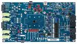


 工商网监
湘ICP备2023018690号
工商网监
湘ICP备2023018690号