Product
Folder
Order
Now
Support &
Community
Tools &
Software
Technical
Documents
TLV61048
ZHCSJH5 – MARCH 2019
采用 SOT-23 封装的 TLV61048 15V 输出电压非同步升压转换器
1 特性
•
•
•
•
•
•
•
•
TLV61048 是一款非同步升压转换器,为由低电压超级
电容器和单芯锂离子电池供电的产品提供电源解决方
案。TLV61048 将电源开关与 4.7A 典型电流限制相集
成,在不影响最大负载交付的情况下增强了输入电源的
放电能力。TLV61048 也支持使用尺寸更小的宽范围外
部电感器和输出电容器来简化设计工作。
输入电压:2.61V 至 5.5V(下降 2.4V)
输出电压最高 15V
集成低侧 FET:输入电压为 3.3V 时,电阻为
85mΩ
4.7A(典型值)开关电流限制
600kHz 或 1MHz 可选开关频率
1µA 关断电流
输出电压精度为 2.5%
轻负载下采用 PFM 运行模式
内部 2ms 软启动时间
热关断保护
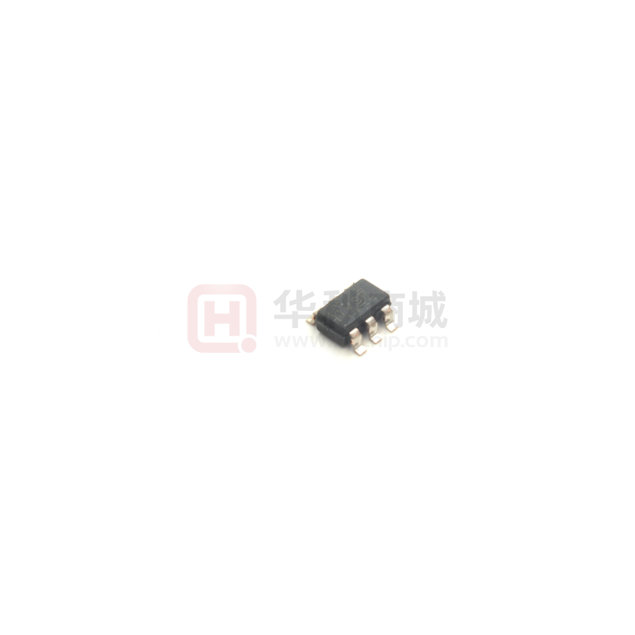
6 引脚 3mm × 3mm SOT-23 封装
通过配置 FREQ 引脚,TLV61048 的可选开关频率为
600kHz 或 1MHz。在轻负载时,该器件会进入 PFM
运行模式来实现更高的效率。TLV61048 具有 2ms 内
置软启动时间,从而可最大程度地降低浪涌电流。
TLV61048 采用 3mm × 3mm 6 引脚 SOT-23 封装。
器件信息(1)
2 应用
•
•
•
器件型号
PLC 备用电源
LCD 偏置电源
直流/直流工业隔离
TLV61048
封装
封装尺寸(标称值)
SOT-23 (6)
2.90mm × 1.60mm
(1) 如需了解所有可用封装,请参阅数据表末尾的可订购产品附
录。
简化原理图
L1
1.5 V ~ 2.6 V
C1
12V
D1
3.3V
VIN
SW
C3
C2
GND
FREQ
R1
ON
OFF
FB
EN
R2
1
本文档旨在为方便起见,提供有关 TI 产品中文版本的信息,以确认产品的概要。 有关适用的官方英文版本的最新信息,请访问 www.ti.com,其内容始终优先。 TI 不保证翻译的准确
性和有效性。 在实际设计之前,请务必参考最新版本的英文版本。
English Data Sheet: SLVSEX0
ADVANCE INFORMATION
•
•
•
1
3 说明
�TLV61048
ZHCSJH5 – MARCH 2019
www.ti.com.cn
目录
1
2
3
4
5
6
7
特性 ..........................................................................
应用 ..........................................................................
说明 ..........................................................................
修订历史记录 ...........................................................
Pin Configuration and Functions .........................
Specifications.........................................................
1
1
1
2
3
4
6.1
6.2
6.3
6.4
6.5
4
4
4
4
5
Absolute Maximum Ratings ......................................
ESD Ratings ............................................................
Recommended Operating Conditions.......................
Thermal Information ..................................................
Electrical Characteristics...........................................
8
8.1 Application Information.............................................. 9
8.2 Typical Applications .................................................. 9
9 Power Supply Recommendations...................... 14
10 Layout................................................................... 14
10.1 Layout Guidelines ................................................. 14
10.2 Layout Example .................................................... 14
11 器件和文档支持 ..................................................... 15
11.1
11.2
11.3
11.4
11.5
11.6
Detailed Description .............................................. 6
7.1
7.2
7.3
7.4
Overview ...................................................................
Functional Block Diagram .........................................
Feature Description...................................................
Device Functional Modes..........................................
Application and Implementation .......................... 9
6
6
6
7
器件支持 ...............................................................
接收文档更新通知 .................................................
社区资源................................................................
商标 .......................................................................
静电放电警告.........................................................
术语表 ...................................................................
15
15
15
15
15
15
12 机械、封装和可订购信息 ....................................... 15
ADVANCE INFORMATION
4 修订历史记录
注:之前版本的页码可能与当前版本有所不同。
2
日期
修订版本
说明
2019 年 3 月
*
初始发行版
Copyright © 2019, Texas Instruments Incorporated
�TLV61048
www.ti.com.cn
ZHCSJH5 – MARCH 2019
5 Pin Configuration and Functions
DBV Package
6-Pin SOT-23
Top View
SW
FREQ
GND
VIN
FB
EN
Pin Functions
NO.
NAME
I/O
DESCRIPTION
1
SW
PWR
The switch pin of the converter. It is connected to the drain of the internal power MOSFET.
2
GND
PWR
Ground
3
FB
I
Voltage feedback of adjustable output voltage. Connected to the center tap of a resistor
divider to program the output voltage.
4
EN
I
Enable logic input. Logic high voltage enables the device. Logic low voltage disables the
device and turns it into shutdown mode.
5
VIN
I
IC power supply input
6
FREQ
I
Frequency select pin. The device operates at 600 kHz if FREQ is left floating and at 1 MHz if
connected to GND.
Copyright © 2019, Texas Instruments Incorporated
ADVANCE INFORMATION
PIN
3
�TLV61048
ZHCSJH5 – MARCH 2019
www.ti.com.cn
6 Specifications
6.1 Absolute Maximum Ratings
over operating free-air temperature range (unless otherwise noted)
(1)
MIN
MAX
– 0.3
6
V
SW
–0.3
18
V
FB
-0.3
3.6
V
–40
150
°C
VIN, EN, FREQ
Voltage range at terminals
(2)
Operating junction temperature range, TJ
(1)
(2)
UNIT
Stresses beyond those listed under Absolute Maximum Ratings may cause permanent damage to the device. These are stress ratings
only, which do not imply functional operation of the device at these or any other conditions beyond those indicated under Recommended
Operating Conditions. Exposure to absolute-maximum-rated conditions for extended periods may affect device reliability.
All voltage values are with respect to network ground terminal.
6.2 ESD Ratings
V(ESD) (1)
ADVANCE INFORMATION
(1)
(2)
(3)
Electrostatic discharge
VALUE
UNIT
Human body model (HBM), per ANSI/ESDA/JEDEC JS-001, all pins (2)
±2000
V
Charged device model (CDM), per JEDEC specification JESD22-C101, all pins (3)
±500
V
Electrostatic discharge (ESD) to measure device sensitivity and immunity to damage caused by assembly line electrostatic discharges in
to the device.
JEDEC document JEP155 states that 500-V HBM allows safe manufacturing with a standard ESD control process.
JEDEC document JEP157 states that 250-V CDM allows safe manufacturing with a standard ESD control process.
6.3 Recommended Operating Conditions
over operating free-air temperature range (unless otherwise noted)
MIN
TYP
MAX
UNIT
VIN
Input voltage range
2.6
5.5
VOUT
Output voltage range
3.3
14
V
V
L
Effective inductance range
2.2
4.7
10
µH
CIN
Effective input capacitance range
0.22
1
COUT
Effective output capacitance range
4.7
TJ
Operating junction temperature
–40
µF
µF
125
°C
6.4 Thermal Information
TLV61048
THERMAL METRIC (1)
DBV (SOT23)
UNIT
6 PINS
RθJA
Junction-to-ambient thermal resistance
177.7
RθJC(top)
Junction-to-case (top) thermal resistance
120.6
RθJB
Junction-to-board thermal resistance
33.2
ψJT
Junction-to-top characterization parameter
21.5
ψJB
Junction-to-board characterization parameter
32.6
RθJC(bot)
Junction-to-case (bottom) thermal resistance
n/a
(1)
4
°C/W
For more information about traditional and new thermal metrics, see the IC Package Thermal Metrics application report, SPRA953.
Copyright © 2019, Texas Instruments Incorporated
�TLV61048
www.ti.com.cn
ZHCSJH5 – MARCH 2019
6.5 Electrical Characteristics
TA = –40°C to 85°C, VIN = 3.3 V. Typical values are at TA = 25°C, unless otherwise noted.
PARAMETER
TEST CONDITIONS
MIN
TYP
MAX
2.55
2.61
UNIT
POWER SUPPLY
VIN
Input voltage range
2.6
VIN rising
VIN_UVLO
Under voltage lockout threshold
VIN_HYS
VIN UVLO hysteresis
IQ_VIN
Quiescent current into VIN pin
IC enabled, no load, no switching
ISD
Shutdown current into VIN pin
IC disabled, VIN = 2.6 V to 5.5 V, TA = 25°C
VIN falling
2.3
5.5
2.4
150
V
V
mV
100
µA
1.0
µA
OUTPUT
VOUT
Output voltage range
3.3
PWM mode, TJ=-40°C to 125°C
VREF
Feedback voltage
IFB_LKG
Leakage current into FB pin
TA = 25°C
ISW_LKG
Leakage current into SW pin
IC disabled, SW = 5.5V
0.78
PFM mode, TA=25°C
0.8
15
V
0.82
V
50
nA
500
nA
0.81
V
POWER SWITCH
Low-side MOSFET on resistance
Vin = 3.3, Vout = 12V
85
mΩ
Default, SW = 1.5V
480
550
620
kHz
Default, SW = 2.6V
1020
1150
1280
kHz
fSW
Switching frequency
tOFF_min
Min. off time
600kHz, SW = 1.5V
ILIM_SW
Peak switch current limit
600kHz, VIN = 3.3V
tSTARTUP
Startup time
130
3.8
4.7
ADVANCE INFORMATION
RDS(on)
ns
5.6
2
A
ms
LOGIC INTERFACE
VEN_H
EN Logic high threshold
VEN_L
EN Logic low threshold
REN
EN Pull Down Resistor
RFREQ
FREQ pull up resistance
VFREQ_H
FREQ logic high threshold
VFREQ_L
FREQ logic low threshold
1.2
0.4
V
V
1
MΩ
800
kΩ
1.2
0.4
V
V
PROTECTION
TSD
Thermal shutdown threshold
TJ rising
TSD_HYS
Thermal shutdown hysteresis
TJ falling below TSD
版权 © 2019, Texas Instruments Incorporated
150
°C
20
°C
5
�TLV61048
ZHCSJH5 – MARCH 2019
www.ti.com.cn
7 Detailed Description
7.1 Overview
The TLV61048 is a non-synchronous boost converter supporting output voltage up to 15 V with input ranging
from 2.61 V to 5.5 V. The TLV61048 integrates a power switch with current limit up to 4.7 A (typical). The device
operates in a current mode scheme with quasi-constant frequency with internal loop compensation built in. The
switching frequency is selectable between 600 kHz and 1 MHz. There is internal fixed soft start time which is 2
ms typically to control the inrush current during startup.
Topology of the TLV61048 boost converter is adaptive off-time with peak current control, which provides superior
load and line transient responses. The selectable switching frequency offers the possibility to optimize the design
either for the use of small sized inductor (1 MHz) or for higher system efficiency (600 kHz).
The converter operates in continuous conduction mode (CCM) when the inductor valley current is above zero,
while switches into discontinuous conduction mode (DCM) if valley current crossing zero. If the load is further
lowered, the device enters into PFM operation to achieve even higher efficiency.
7.2 Functional Block Diagram
ADVANCE INFORMATION
VIN
5
1
SW
6
FREQ
3
FB
Gate Driver
UVLO
Current
Limit
EN
4
Control
Logic
PWM Generator
On Time
GND
2
Thermal Shutdown
VIN
SW
Off Time
EA
SS
REF
7.3 Feature Description
7.3.1 Undervoltage Lockout
An undervoltage lockout (UVLO) circuit stops the operation of the converter when the input voltage drops below
the typical UVLO threshold of 2.4 V. A hysteresis of 150 mV is added so that the device cannot be enabled again
until the input voltage goes up to 2.55 V. This function is implemented in order to prevent malfunctioning of the
device when the input voltage is between 2.4 V and 2.55 V.
6
版权 © 2019, Texas Instruments Incorporated
�TLV61048
www.ti.com.cn
ZHCSJH5 – MARCH 2019
Feature Description (接
接下页)
7.3.2 Enable and Disable
When the input voltage is above typical UVLO rising threshold of 2.55 V and the EN pin is pulled high, the
TLV61048 is enabled. When the EN pin is pulled low, the TLV61048 stops the PWM switch and turns off the low
side switch. The EN pin has an internal pull-down resistance of 1MΩ, the device is disabled when the EN pin is
floating. In shutdown mode, less than 1-µA input current is consumed.
7.3.3 Soft Start
The soft-start feature helps the regulator to gradually reach the steady state operating point, thus reducing startup stresses and surge. When the input voltage is applied, the output capacitor is charged to VIN through the
inductor and high side rectifier diode. After reaching the 2.55 V (typical) UVLO threshold, the internal soft-start
control circuit initiates to ramp the reference voltage to 0.8 V within 2 ms (typical), while the low side FET starts
switching after output capacitor is charged to the input voltage.
The frequency select pin FREQ allows to set the switching frequency of the device to 600 kHz (FREQ = floating)
or 1 MHz (FREQ = GND). Higher switching frequency improves load transient response but reduces efficiency
slightly. The other benefit of higher switching frequency is lower output ripple voltage.
7.4 Device Functional Modes
The TLV61048 has two operation modes: PWM mode and PFM mode.
7.4.1 PWM Mode
The TLV61048 uses a quasi-constant frequency pulse width modulation (PWM) at moderate to heavy load
currents. Based on the VIN/VOUT ratio, a circuit predicts the required off-time. At the beginning of the switching
cycle, the integrated NMOS switching FET, shown in the functional block diagram, is turned on. The input voltage
is applied across the inductor and the inductor current ramps up. In this phase, the output capacitor is discharged
by the load current. When the inductor current hits the current threshold that is set by the error amplifier output,
the PWM switch is turned off, and the external power diode is forward-biased. The inductor transfers its stored
energy to replenish the output capacitor and supply the load. When the off-time is expired, the next switching
cycle starts again. The error amplifier compares the FB pin voltage with an internal reference, and its output
determines the duty cycle of the PWM switching.
The TLV61048 has a built-in compensation circuit that can accommodate a wide range of input and output
voltages for stable operation.
7.4.2 PFM Mode
The TLV61048 integrates a power save mode with pulse frequency modulation (PFM) to improve efficiency at
light load. When the load current decreases, the inductor peak current set by the output of the error amplifier
declines to regulate the output voltage. When the inductor peak current hits the low limit (400 mA typical), the
output voltage exceeds the set threshold voltage as the load current decreases further. When the FB voltage hits
the PFM reference voltage, the TLV61048 goes into power-save mode. In the power-save mode, the device only
switches when the output voltage trips below a set threshold voltage. It ramps up the output with several pulses
and enters the power save mode when the output voltage exceeds the set threshold voltage.
版权 © 2019, Texas Instruments Incorporated
7
ADVANCE INFORMATION
7.3.4 Frequency Select (FREQ)
�TLV61048
ZHCSJH5 – MARCH 2019
www.ti.com.cn
Device Functional Modes (接
接下页)
Output
Voltage
PFM mode at light load
1.01 x VOUT_NOM
VOUT_NOM
ADVANCE INFORMATION
PWM mode at heavy load
8
版权 © 2019, Texas Instruments Incorporated
�TLV61048
www.ti.com.cn
ZHCSJH5 – MARCH 2019
8 Application and Implementation
注
Information in the following applications sections is not part of the TI component
specification, and TI does not warrant its accuracy or completeness. TI’s customers are
responsible for determining suitability of components for their purposes. Customers should
validate and test their design implementation to confirm system functionality.
8.1 Application Information
TLV61048 is a boost DC/DC converter integrating a power switch and loop compensation circuits. The device
supports up to 15-V output with the input range from 2.61 V to 5.5 V. The device can operate down to 1.5 V if an
external 3.3-V bias supply is applied to the VIN pin. The TLV61048 adopts the current-mode control with
adaptive constant off-time. The switching frequency is quasi-constant and selectable between 600 kHz and 1
MHz. The following design procedure can be used to select component values for the TLV61048.
8.2.1 12-V Output Boost Converter With External Bias
In this design example, TLV61048 VIN pin is supplied by an external 3.3-V bias voltage to keep internal circuitry
on in order to extend power stage operating VIN to 1.5 V. 600-kHz switching frequency is selected to reduce
switching loss in order to improve overall efficiency.
L1
1.5 V ~ 2.6 V
VIN
C1
1.0uF
4.7uH
12 V
3.3 V
Bias VIN
VIN
SW
C3
0.1uF
C2
10uF
R1
FREQ
GND
1.5M
TLV61048
ON
OFF
FB
EN
R2
107k
图 1. 12-V Boost Converter With External Bias
8.2.1.1 Design Requirements
For this design example, see parameters are shown in 表 1:
表 1. Design Requirements
PARAMETERS
VALUE
Power input voltage
1.5 V to 2.7 V
Control input voltage
3.3 V
Output voltage
12 V
Frequency
600 kHz
Output current
0 - 100 mA
版权 © 2019, Texas Instruments Incorporated
9
ADVANCE INFORMATION
8.2 Typical Applications
�TLV61048
ZHCSJH5 – MARCH 2019
www.ti.com.cn
8.2.1.2 Detailed Design Procedure
8.2.1.2.1 Programming the Output Voltage
Output voltage is programmed via external resistor divider. By selecting the external resistor divider R1 and R2,
as shown in 公式 1, the output voltage is programmed to the desired value. When the output voltage is regulated,
the typical voltage at the FB pin is VREF of 800 mV.
§V
R1 ¨ OUT
© VREF
·
1¸ u R2
¹
where
•
•
VOUT is the desired output voltage
VREF is the internal reference voltage at the FB pin
(1)
For best accuracy, R2 should be kept smaller than 150 kΩ to ensure the current flowing through R2 is at least
100 times larger than the FB pin leakage current. Changing R2 towards a lower value increases the immunity
against noise injection. Changing the R2 towards a higher value reduces the quiescent current for achieving
higher efficiency at low load currents.
8.2.1.2.2 Inductor Selection
ADVANCE INFORMATION
Because the selection of the inductor affects steady state operation, transient behavior, and loop stability, the
inductor is the most important component in power regulator design. There are three important inductor
specifications, inductor value, saturation current, and DC resistance (DCR). The TLV61048 is designed to work
with inductor values between 2.2 µH and 10 µH. Use 公式 2 to 公式 4 to calculate the peak current of the
application inductor. To calculate the current in the worst case, use the minimum input voltage, maximum output
voltage, and maximum load current of the application. To have enough design margin, choose the inductor value
with –30% tolerance, and a low power-conversion efficiency for the calculation. In a boost regulator, the inductor
dc current can be calculated with 公式 2.
VOUT u IOUT
IL(DC)
VIN u K
where
•
•
•
•
VOUT = output voltage
IOUT = output current
VIN = input voltage
η = power conversion efficiency, use 80% for most applications
(2)
The inductor ripple current is calculated with the 公式 3 for an asynchronous boost converter in continuous
conduction mode (CCM).
VIN u VOUT 0.8V VIN
'IL(P P)
L u fSW u VOUT 0.8V
where
•
•
•
•
•
ΔIL(P-P) = inductor ripple current
L = inductor value
fSW = switching frequency
VOUT = output voltage
VIN = input voltage
Therefore, the inductor peak current is calculated with 公式 4.
'IL P P
IL P IL DC
2
(3)
(4)
Normally, it is advisable to work with an inductor peak-to-peak current of less than 40% of the average inductor
current for maximum output current. A smaller ripple from a larger valued inductor reduces the magnetic
hysteresis losses in the inductor and EMI. However, in the same way, load transient response time is increased.
表 2 lists the recommended inductor for the TLV61048 in the 600-kHz configuration.
10
版权 © 2019, Texas Instruments Incorporated
�TLV61048
www.ti.com.cn
ZHCSJH5 – MARCH 2019
表 2. Recommended Inductors for the TLV61048 at 600-kHz Configuration
(1)
PART NUMBER
L (µH)
DCR MAX (mΩ)
SATURATION CURRENT
TYPICAL (A)
SIZE (L×W×H) (mm)
VENDOR (1)
SWPA5040S4R7NT
4.7
39
3.9
5×5×4
Sunlord
Coilcraft
XAL4030-472ME
4.7
44.1
4.5
4×4×3
SWPA5040S100MT
10
83
2.9
5×5×4
Sunlord
XAL4040-103ME
10
92.4
3
4×4×4
Coilcraft
See Third-party Products Disclaimer
8.2.1.2.3 Input and Output Capacitor Selection
The output capacitor is mainly selected to meet the requirements for output ripple and loop stability. This ripple
voltage is related to the capacitor’s capacitance and its equivalent series resistance (ESR). Assuming a ceramic
capacitor with zero ESR, the minimum capacitance needed for a given ripple can be calculated by:
IOUT u DMAX
COUT
fSW u VRIPPLE
•
•
DMAX = maximum switching duty cycle
VRIPPLE = peak to peak output voltage ripple
(5)
The ESR impact on the output ripple must be considered if tantalum or aluminum electrolytic capacitors are
used.
Take care when evaluating the derating of a ceramic capacitor under DC bias, aging, and AC signal. For
example, the DC bias can significantly reduce capacitance. A ceramic capacitor can lose more than 50% of its
capacitance at its rated voltage. Therefore, always leave margin on the voltage rating to ensure adequate
capacitance at the required output voltage.
TI recommends using the output capacitor with effective capacitance in the range of 4.7 µF to 10 µF for 600-kHz
configuration. TI also recommends placing a small 1 µF capacitor right across the rectifier diode cathode to the
GND pin of the TLV61048 to reduce the high RMS current loop's inductance. The output capacitor affects the
small signal control loop stability of the boost regulator. If the output capacitor is below the range, the boost
regulator can potentially become unstable. Increasing the output capacitor makes the output voltage ripple
smaller in PWM mode. 表 3 lists the recommended capacitor for the TLV61048.
表 3. Recommended Output Capacitors for the TLV61048
(1)
PART NUMBER
COUT (µF)
RATING
PACKAGE
VENDOR (1)
TMK316BLD106KL
10
25 V, X5R
1206
Taiyo Yuden
CC1206KKX5R8BB106
10
25 V, X5R
1206
Yageo
See Third-party Products Disclaimer.
版权 © 2019, Texas Instruments Incorporated
11
ADVANCE INFORMATION
where
�TLV61048
ZHCSJH5 – MARCH 2019
www.ti.com.cn
For input capacitor, a ceramic capacitor with more than 1 µF is enough for most applications.
8.2.1.3 Application Curves
SW
5 V/div
SW
5 V/div
Vout (AC)
20 mV/div
Vout (AC)
50 mV/div
Inductor
Current
300 mA/div
Inductor
Current
400 mA/div
VIN = 2.5 V
VOUT = 12 V
IOUT = 0.1 A
VIN = 2.5 V
ADVANCE INFORMATION
图 2. Switching Waveform in CCM
VOUT = 12 V
IOUT = 10 mA
图 3. Switching Waveform in PFM
EN
2 V/div
EN
2 V/div
Vout
3 V/div
Vout
3 V/div
Inductor
Current
300 mA/div
Inductor
Current
300 mA/div
图 4. Start-up Waveform
图 5. Shutdown Waveform
Vout (AC)
300 mV/div
Vout (AC)
100 mV/div
Input
Voltage
1 V/div
Output
Current
50 mA/div
VIN= 2.5 V
VOUT= 12 V
IOUT= 0.06A to 0.1
A
VIN= 1.5 V to 2.6 V
VOUT= 12 V
IOUT= 0.1 A
图 7. Line Transient
图 6. Load Transient
12
版权 © 2019, Texas Instruments Incorporated
�TLV61048
www.ti.com.cn
ZHCSJH5 – MARCH 2019
8.2.2 15-V Output Boost Converter
In this design example, TLV61048 is configured to output 15-V DC voltage. 1-MHz switching frequency is
selected to reduce output ripple and improve load transient performance. TI recommends placing an RC snubber
from the switch node to the ground node to ensure voltage spike does not exceed the specified absolute
maximum rating.
L1
3.3 µH
C1
1 µF
15 V
VIN
SW
C2
10 µF
FREQ
GND
R1
2M
ADVANCE INFORMATION
TLV61048
FB
EN
R2
113 k
图 8. 15-V Boost Converter
8.2.2.1 Design Requirements
表 4. Design Requirements
PARAMETER
VALUE
Power input voltage
2.6 V to 5.5 V
Output voltage
15 V
Frequency
1 MHz
Output current
0 to 300 mA
8.2.2.2 Detailed Design Procedure
8.2.2.2.1 Inductor Selection
Load transient and loop response performance is optimized at 1-MHz configuration, a smaller inductance is
selected to push the right-half-plane-zero to a higher frequency beyond the crossover frequency of the control
loop. The recommended inductors for 1-MHz operation are listed in 表 5.
表 5. Recommended Inductors for the TLV61048 at 1-MHz Configuration
DCR MAX (mΩ)
SATURATION CURRENT
TYPICAL (A)
SIZE (LxWxH) (mm)
2.2
25
5.6
5×5×4
Sunlord
2.2
38.7
5.6
4×4×3
Coilcraft
3.3
31
4.6
5×5×4
Sunlord
3.3
28.6
5.5
4×4×4
Coilcraft
PART NUMBER
L (µH)
SWPA5040S2R2NT
XAL4020-222ME
SWPA5040S3R3NT
XAL4030-332ME
(1)
VENDOR (1)
See Third-party Products Disclaimer.
8.2.2.2.2 Input and Output Capacitor Selection
For 1-MHz configuration, use the information provided in Input and Output Capacitor Selection.
版权 © 2019, Texas Instruments Incorporated
13
�TLV61048
ZHCSJH5 – MARCH 2019
www.ti.com.cn
9 Power Supply Recommendations
The device is designed to operate from an input voltage supply range between 1.5 V to 5.5 V. This input supply
must be well regulated. If the input supply is located more than a few inches from the converter, additional bulk
capacitance may be required in addition to the ceramic bypass capacitors. A typical choice is an electrolytic or
tantalum capacitor with a value of 47 µF. Output current of the input power supply must be rated according to the
supply voltage, output voltage and output current of the TLV61048.
10 Layout
10.1 Layout Guidelines
As for all switching power supplies, especially those running at high switching frequency and high currents,
layout is an important design step. If the layout is not carefully done, the regulator could suffer from instability
and noise problems. To maximize efficiency, switch rise and fall time are very fast. To prevent radiation of high
frequency noise (for example, EMI), proper layout of the high-frequency switching path is essential. Minimize the
length and area of all traces connected to the SW pin, and always use a ground plane under the switching
regulator to minimize interplane coupling. The input capacitor must not only to be close to the VIN pin, but also to
the GND in in order to reduce input supply ripple.
10.2 Layout Example
GND
ADVANCE INFORMATION
The most critical current path for all boost converters is from the switching FET, through the rectifier diode, then
the output capacitors, and back to ground of the switching FET. This high current path contains nanosecond rise
and fall time and must be kept as short as possible. Therefore, the output capacitor must not only to be close to
the VOUT pin, but also to the GND pin to reduce the overshoot at the SW pin and VOUT pin.
VIN
FREQ
VIN
EN
GND
SW
GND
FB
VOUT
图 9. TLV61048 Layout
14
版权 © 2019, Texas Instruments Incorporated
�TLV61048
www.ti.com.cn
ZHCSJH5 – MARCH 2019
11 器件和文档支持
11.1 器件支持
11.1.1 第三方产品免责声明
TI 发布的与第三方产品或服务有关的信息,不能构成与此类产品或服务或保修的适用性有关的认可,不能构成此类
产品或服务单独或与任何 TI 产品或服务一起的表示或认可。
11.2 接收文档更新通知
要接收文档更新通知,请导航至 TI.com.cn 上的器件产品文件夹。单击右上角的通知我 进行注册,即可每周接收产
品信息更改摘要。有关更改的详细信息,请查看任何已修订文档中包含的修订历史记录。
11.3 社区资源
TI E2E™ Online Community TI's Engineer-to-Engineer (E2E) Community. Created to foster collaboration
among engineers. At e2e.ti.com, you can ask questions, share knowledge, explore ideas and help
solve problems with fellow engineers.
Design Support TI's Design Support Quickly find helpful E2E forums along with design support tools and
contact information for technical support.
11.4 商标
E2E is a trademark of Texas Instruments.
All other trademarks are the property of their respective owners.
11.5 静电放电警告
ESD 可能会损坏该集成电路。德州仪器 (TI) 建议通过适当的预防措施处理所有集成电路。如果不遵守正确的处理措施和安装程序 , 可
能会损坏集成电路。
ESD 的损坏小至导致微小的性能降级 , 大至整个器件故障。 精密的集成电路可能更容易受到损坏 , 这是因为非常细微的参数更改都可
能会导致器件与其发布的规格不相符。
11.6 术语表
SLYZ022 — TI 术语表。
这份术语表列出并解释术语、缩写和定义。
12 机械、封装和可订购信息
以下页面包含机械、封装和可订购信息。这些信息是指定器件的最新可用数据。数据如有变更,恕不另行通知,且
不会对此文档进行修订。如需获取此产品说明书的浏览器版本,请查阅左侧的导航栏。
版权 © 2019, Texas Instruments Incorporated
15
ADVANCE INFORMATION
下列链接提供到 TI 社区资源的连接。链接的内容由各个分销商“按照原样”提供。这些内容并不构成 TI 技术规范,
并且不一定反映 TI 的观点;请参阅 TI 的 《使用条款》。
�PACKAGE OPTION ADDENDUM
www.ti.com
10-Dec-2020
PACKAGING INFORMATION
Orderable Device
Status
(1)
Package Type Package Pins Package
Drawing
Qty
Eco Plan
(2)
Lead finish/
Ball material
MSL Peak Temp
Op Temp (°C)
Device Marking
(3)
(4/5)
(6)
TLV61048DBVR
ACTIVE
SOT-23
DBV
6
3000
RoHS & Green
NIPDAU
Level-1-260C-UNLIM
-40 to 125
1VSF
TLV61048DBVT
ACTIVE
SOT-23
DBV
6
250
RoHS & Green
NIPDAU
Level-1-260C-UNLIM
-40 to 125
1VSF
(1)
The marketing status values are defined as follows:
ACTIVE: Product device recommended for new designs.
LIFEBUY: TI has announced that the device will be discontinued, and a lifetime-buy period is in effect.
NRND: Not recommended for new designs. Device is in production to support existing customers, but TI does not recommend using this part in a new design.
PREVIEW: Device has been announced but is not in production. Samples may or may not be available.
OBSOLETE: TI has discontinued the production of the device.
(2)
RoHS: TI defines "RoHS" to mean semiconductor products that are compliant with the current EU RoHS requirements for all 10 RoHS substances, including the requirement that RoHS substance
do not exceed 0.1% by weight in homogeneous materials. Where designed to be soldered at high temperatures, "RoHS" products are suitable for use in specified lead-free processes. TI may
reference these types of products as "Pb-Free".
RoHS Exempt: TI defines "RoHS Exempt" to mean products that contain lead but are compliant with EU RoHS pursuant to a specific EU RoHS exemption.
Green: TI defines "Green" to mean the content of Chlorine (Cl) and Bromine (Br) based flame retardants meet JS709B low halogen requirements of