Product
Folder
Order
Now
Support &
Community
Tools &
Software
Technical
Documents
TLV6710
SNVSAV4B – JANUARY 2018 – REVISED OCTOBER 2018
TLV6710 Micropower, 36-V Window Comparator With 400-mV Reference
1 Features
3 Description
•
•
•
The TLV6710 is a high voltage window comparator
that operates over a 1.8 V to 36 V range. The device
has two high-accuracy comparators with an internal
400-mV reference and two open-drain outputs rated
to 25 V. The TLV6710 can be used as a window
comparator or as two independent comparators; the
monitored voltage can be set with the use of external
resistors.
1
•
•
•
•
•
High Supply Voltage Range: 1.8 V to 36 V
Adjustable Threshold: Down to 400 mV
High Threshold Accuracy:
– 0.25% (Typical)
– 0.75% Max Over Temperature
Low Quiescent Current: 7 µA (Typical)
Open-Drain Outputs
Internal Hysteresis: 5.5 mV (Typical)
Temperature Range: –40°C to 125°C
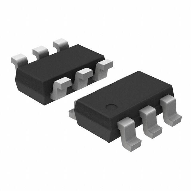
Package: Thin SOT-23-6
OUTA is driven low when the voltage at INA+ drops
below (VITP – VHYS), and goes high when the voltage
returns above the respective threshold (VITP). OUTB
is driven low when the voltage at INB– rises above
VITP, and goes high when the voltage drops below the
respective threshold (VITP – VHYS). Both comparators
in the TLV6710 include built-in hysteresis to reject
brief glitches, thereby ensuring stable output
operation without false triggering.
2 Applications
•
•
•
•
•
•
•
•
Notebook PCs and Tablets
Smartphones
Digital Cameras
Video Game Controllers
Relays and Circuit Breakers
Portable Medical Devices
Door and Window Sensors
Portable- and Battery-Powered Products
The TLV6710 is available in a Thin SOT-23-6
package and is specified over the junction
temperature range of –40°C to 125°C.
Device Information(1)
PART NUMBER
TLV6710
PACKAGE
SOT-23 (6)
BODY SIZE (NOM)
2.90 mm × 1.60 mm
(1) For all available packages, see the package option addendum
at the end of the data sheet.
Simplified Block Diagram
VPULL-UP
(Up To 25 V)
1.8 V to 36 V
VDD
OUTA
INA+
OUTB
INB–
Reference
GND
1
An IMPORTANT NOTICE at the end of this data sheet addresses availability, warranty, changes, use in safety-critical applications,
intellectual property matters and other important disclaimers. PRODUCTION DATA.
�TLV6710
SNVSAV4B – JANUARY 2018 – REVISED OCTOBER 2018
www.ti.com
Table of Contents
1
2
3
4
5
6
7
8
Features ..................................................................
Applications ...........................................................
Description .............................................................
Revision History.....................................................
Device Comparison Table.....................................
Pin Configuration and Functions .........................
Specifications.........................................................
1
1
1
2
3
3
4
7.1
7.2
7.3
7.4
7.5
7.6
7.7
4
4
4
4
5
6
7
Absolute Maximum Ratings .....................................
ESD Ratings..............................................................
Recommended Operating Conditions.......................
Thermal Information ..................................................
Electrical Characteristics...........................................
Timing Requirements ................................................
Typical Characteristics ..............................................
Detailed Description ............................................ 10
8.1 Overview ................................................................. 10
8.2 Functional Block Diagram ....................................... 10
8.3 Feature Description................................................. 11
8.4 Device Functional Modes........................................ 11
9
Application and Implementation ........................ 12
9.1 Application Information............................................ 12
9.2 Typical Application ................................................. 15
9.3 Do's and Don'ts ....................................................... 17
10 Power Supply Recommendations ..................... 18
11 Layout................................................................... 19
11.1 Layout Guidelines ................................................. 19
11.2 Layout Example .................................................... 19
12 Device and Documentation Support ................. 20
12.1
12.2
12.3
12.4
12.5
12.6
12.7
Device Support......................................................
Documentation Support ........................................
Receiving Notification of Documentation Updates
Community Resources..........................................
Trademarks ...........................................................
Electrostatic Discharge Caution ............................
Glossary ................................................................
20
20
20
20
20
20
20
13 Mechanical, Packaging, and Orderable
Information ........................................................... 20
4 Revision History
Changes from Revision A (April 2018) to Revision B
•
Changed output Description text from 36V to 25V on front page Simplified Block Diagram, Description and
Application Information sections. ........................................................................................................................................... 1
Changes from Original (January 2018) to Revision A
•
2
Page
Page
Changed Advance Information to Production Data ............................................................................................................... 1
Submit Documentation Feedback
Copyright © 2018, Texas Instruments Incorporated
Product Folder Links: TLV6710
�TLV6710
www.ti.com
SNVSAV4B – JANUARY 2018 – REVISED OCTOBER 2018
5 Device Comparison Table
Table 1. TLV67xx Integrated Comparator Family
PART NUMBER
CONFIGURATION
OPERATING
VOLTAGE RANGE
THRESHOLD ACCURACY OVER
TEMPERATURE
TLV6700
Window
1.8V to 18V
1%
TLV6703
Non-Inverting Single Channel
1.8V to 18V
1%
TLV6710
Window
1.8V to 36V
0.75%
TLV6713
Non-Inverting Single Channel
1.8V to 36V
0.75%
6 Pin Configuration and Functions
DDC Package
SOT-6
(Top View)
OUTA
1
6
OUTB
GND
2
5
VDD
INA
3
4
INB
Pin Functions
PIN
NAME
NO.
I/O
DESCRIPTION
GND
2
—
Ground
INA
3
I
Comparator A input. This pin is connected to the voltage to be monitored with the use of an
external resistor divider. When the voltage at this terminal drops below the threshold voltage
VIT–(INA), OUTA is driven low.
INB
4
I
Comparator B input. This pin is connected to the voltage to be monitored with the use of an
external resistor divider. When the voltage at this terminal exceeds the threshold voltage
VIT+(INB), OUTB is driven low.
OUTA
1
O
INA comparator open-drain output. OUTA is driven low when the voltage at this comparator
is less than VIT–(INA). The output goes high when the sense voltage rises above VIT+(INA).
OUTB
6
O
INB comparator open-drain output. OUTB is driven low when the voltage at this comparator
exceeds VIT+(INB). The output goes high when the sense voltage falls below VIT–(INB).
VDD
5
I
Supply voltage input. Connect a 1.8-V to 36-V supply to VDD to power the device. It is good
analog design practice to place a 0.1-µF ceramic capacitor close to this pin.
Submit Documentation Feedback
Copyright © 2018, Texas Instruments Incorporated
Product Folder Links: TLV6710
3
�TLV6710
SNVSAV4B – JANUARY 2018 – REVISED OCTOBER 2018
www.ti.com
7 Specifications
7.1 Absolute Maximum Ratings
Over operating junction temperature range, unless otherwise noted. (1)
Voltage
(2)
Current
(2)
MAX
UNIT
–0.3
+40
V
VOUTA, VOUTB
–0.3
+28
V
VINA, VINB
–0.3
+7
V
40
mA
Output pin current
Temperature
(1)
MIN
VDD
Operating junction, TJ
–40
+125
°C
Storage temperature, Tstg
–65
+150
°C
Stresses beyond those listed under Absolute Maximum Ratings may cause permanent damage to the device. These are stress ratings
only, which do not imply functional operation of the device at these or any other conditions beyond those indicated under Recommended
Operating Conditions. Exposure to absolute-maximum-rated conditions for extended periods may affect device reliability.
All voltages are with respect to network ground terminal.
7.2 ESD Ratings
VALUE
V(ESD)
(1)
(2)
Electrostatic discharge
Human-body model (HBM), per ANSI/ESDA/JEDEC JS-001 (1)
±2000
Charged-device model (CDM), per JEDEC specification JESD22-C101 (2)
±500
UNIT
V
JEDEC document JEP155 states that 500-V HBM allows safe manufacturing with a standard ESD control process.
JEDEC document JEP157 states that 250-V CDM allows safe manufacturing with a standard ESD control process.
7.3 Recommended Operating Conditions
over operating junction temperature range (unless otherwise noted)
MIN
VDD
Supply pin voltage
VINA, VINB
NOM
MAX
UNIT
1.8
36
V
Input pin voltage
0
1.7
V
VOUTA, VOUTB
Output pin voltage
0
25
V
IOUTA, IOUTB
Output pin current
10
mA
TJ
Junction temperature
+125
°C
0
–40
+25
7.4 Thermal Information
TLV6710
THERMAL METRIC (1)
DDC (SOT)
UNITS
6 PINS
RθJA
Junction-to-ambient thermal resistance
201.6
°C/W
RθJC(top)
Junction-to-case (top) thermal resistance
47.8
°C/W
RθJB
Junction-to-board thermal resistance
51.2
°C/W
ψJT
Junction-to-top characterization parameter
0.7
°C/W
ψJB
Junction-to-board characterization parameter
50.8
°C/W
RθJC(bot)
Junction-to-case (bottom) thermal resistance
N/A
°C/W
(1)
4
For more information about traditional and new thermal metrics, see the Semiconductor and IC Package Thermal Metrics application
report (SPRA953).
Submit Documentation Feedback
Copyright © 2018, Texas Instruments Incorporated
Product Folder Links: TLV6710
�TLV6710
www.ti.com
SNVSAV4B – JANUARY 2018 – REVISED OCTOBER 2018
7.5 Electrical Characteristics
Over the operating temperature range of TJ = –40°C to +125°C, 1.8 V ≤ VDD < 36 V, and pullup resistors RP1,2 = 100 kΩ,
unless otherwise noted. Typical values are at TJ = 25°C and VDD = 12 V.
PARAMETER
VDD
TEST CONDITIONS
Supply voltage range
MIN
TYP
1.8
(1)
MAX
36
VOL ≤ 0.2 V
UNIT
V
V(POR)
Power-on reset voltage
0.8
V
VIT–(INA)
INA pin negative input threshold voltage VDD = 1.8 V to 36 V
397
400
403
mV
VIT+(INA)
INA pin positive input threshold voltage
400
405.5
413
mV
VHYS(INA)
INA pin hysteresis voltage
(HYS = VIT+(INA) – VIT–(INA))
2
5.5
12
mV
VIT–(INB)
INB pin negative input threshold voltage VDD = 1.8 V to 36 V
387
394.5
400
mV
VIT+(INB)
INB pin positive input threshold voltage
397
400
403
mV
VHYS(INB)
INB pin hysteresis voltage
(HYS = VIT+(INB) – VIT–(INB))
2
5.2
12
mV
VOL
Low-level output voltage
VDD = 1.8 V, IOUT = 3 mA
130
250
mV
VDD = 5 V, IOUT = 5 mA
150
250
mV
IIN
Input current (at INA, INB pins)
ID(leak)
Open-drain output leakage current
VDD = 1.8 V and 36 V, VOUT = 25 V
IDD
Supply current
VDD = 1.8 V – 36 V
UVLO
Undervoltage lockout (2)
VDD falling
(1)
(2)
VDD = 1.8 V to 36 V
VDD = 1.8 V to 36 V
VDD = 1.8 V and 36 V, VINA, VINB = 6.5 V
–25
+1
+25
nA
VDD = 1.8 V and 36 V, VINA, VINB = 0.1 V
–15
+1
+15
nA
10
300
nA
8
11
µA
1.5
1.7
V
1.3
The lowest supply voltage (VDD) at which output is active; tr(VDD) > 15 µs/V. If less than V(POR), the output is undetermined.
When VDD falls below UVLO, OUTA is driven low and OUTB goes to high impedance. The outputs cannot be determined if less than
V(POR).
Submit Documentation Feedback
Copyright © 2018, Texas Instruments Incorporated
Product Folder Links: TLV6710
5
�TLV6710
SNVSAV4B – JANUARY 2018 – REVISED OCTOBER 2018
www.ti.com
7.6 Timing Requirements
PARAMETER
TEST CONDITION
MIN
TYP
MAX
UNIT
.tpd(HL)
High-to-low propagation delay
(1)
VDD = 24 V, ±10-mV input overdrive,
RL = 100 kΩ, VOH = 0.9 × VDD, VOL = 250 mV
9.9
µs
tpd(LH)
Low-to-high propagation delay (1)
VDD = 24 V, ±10-mV input overdrive,
RL = 100 kΩ, VOH = 0.9 × VDD, VOL = 250 mV
28.1
µs
Startup delay
VDD = 5 V
155
µs
tr
Output rise time
VDD = 12 V, 10-mV input overdrive,
RL = 100 kΩ, CL = 10 pF, VO = (0.1 to 0.9) × VDD
2.7
µs
tf
Output fall time
VDD = 12 V, 10-mV input overdrive,
RL = 100 kΩ, CL = 10 pF, VO = (0.9 to 0.1) × VDD
0.12
µs
td(start)
(1)
(2)
(2)
High-to-low and low-to-high refers to the transition at the input pins (INA and INB).
During power on, VDD must exceed 1.8 V for at least 150 µs (typ) before the output state reflects the input condition.
VDD
V(POR)
VIT+(INA)
INA
V HYS
VIT±(INA)
OUTA
t pd(LH)
t pd(HL)
t pd(LH)
VIT+(INB)
INB
V HYS
VIT±(INB)
OUTB
t pd(LH)
t pd(HL)
t d(start)
Figure 1. Timing Diagram
6
Submit Documentation Feedback
Copyright © 2018, Texas Instruments Incorporated
Product Folder Links: TLV6710
�TLV6710
www.ti.com
SNVSAV4B – JANUARY 2018 – REVISED OCTOBER 2018
7.7 Typical Characteristics
At TJ = 25°C and VDD = 12 V, unless otherwise noted.
10
22
INA
INB
20
Minimum Pulse Width (Ps)
Supply Current (PA)
8
6
4
TJ = -40qC
TJ = 0qC
TJ = 25qC
TJ = 85qC
TJ = 125qC
2
18
16
14
12
10
8
6
4
2
0
0
0
6
12
18
24
Supply Voltage (V)
30
36
0
5
10
15
20
25
30
Overdrive (%)
D001
35
40
45
50
D011
VDD = 24 V
Figure 2. Supply Current vs Supply Voltage
Figure 3. Minimum Pulse Duration vs
Threshold Overdrive Voltage (1) (1)
400.2
408.5
408
400.05
407
VIT-(INA) (mV)
VIT-(INB) (mV)
407.5
VDD = 1.8 V
VDD = 12 V
VDD = 36 V
406.5
406
405.5
399.9
399.75
399.6
405
VDD = 1.8 V
VDD = 12 V
VDD = 36 V
399.45
404.5
404
-40
-20
0
20
40
60
TJ (qC)
80
100
120
399.3
-40
140
Figure 4. INA Positive Input Threshold Voltage (VIT+(INA)) vs
Temperature
80
100
120
140
D002
395.1
394.8
VIT-(INB) (mV)
VIT+(INB) (mV)
40
60
TJ (qC)
395.4
399.9
399.75
394.5
394.2
393.9
393.6
393.3
399.6
393
-20
0
20
40
60
TJ (qC)
80
100
120
140
392.7
-40
D004
Figure 6. INB Positive Input Threshold Voltage (VIT+(INB)) vs
Temperature
(1)
20
395.7
VDD = 1.8 V
VDD = 12 V
VDD = 36 V
400.05
399.45
-40
0
Figure 5. INA Negative Input Threshold Voltage (VIT–(INA)) vs
Temperature
400.35
400.2
-20
D005
VDD = 1.8 V
VDD = 12 V
VDD = 36 V
-20
0
20
40
60
TJ (qC)
80
100
120
140
D003
Figure 7. INB Negative Input Threshold Voltage (VIT–(INB)) vs
Temperature
Minimum pulse duration required to trigger output high-to-low transition. INA = negative spike below VIT– and INB = positive spike above
VIT+.
Submit Documentation Feedback
Copyright © 2018, Texas Instruments Incorporated
Product Folder Links: TLV6710
7
�TLV6710
SNVSAV4B – JANUARY 2018 – REVISED OCTOBER 2018
www.ti.com
Typical Characteristics (continued)
At TJ = 25°C and VDD = 12 V, unless otherwise noted.
4500
3500
4000
3000
3500
3000
2000
Count
Count
2500
1500
2500
2000
1500
1000
1000
500
500
402
401
400
398
408
407
406
405
404
399
0
0
D020
D022
VIT-(INA) Threshold Voltage (mV)
VIT+(INA) Threshold Voltage (mV)
VDD = 1.8 V
VDD = 1.8 V
Figure 8. INA Positive Input Threshold Voltage (VIT+(INA))
Distribution
Figure 9. INA Negative Input Threshold Voltage (VIT–(INA))
Distribution
3000
3500
2500
3000
2500
Count
1500
1000
2000
1500
397
396
393
402
401
0
400
0
399
500
398
500
395
1000
394
Count
2000
D021
D023
VIT+(INB) Threshold Voltage (mV)
VIT-(INB) Threshold Voltage (mV)
VDD = 1.8 V
Figure 10. INB Positive Input Threshold Voltage (VIT+(INB))
Distribution
Figure 11. INB Negative Input Threshold Voltage (VIT–(INB))
Distribution
12
3.3
VDD = 1.8 V, INA to OUTA
VDD = 36 V, INA to OUTA
VDD = 1.8 V, INB to OUTB
VDD = 36 V, INB to OUTB
11
10
Low-to-High Propagation Delay (Ps)
High-to-Low Propagation Delay (Ps)
VDD = 1.8 V
9
8
7
6
5
-40
-20
0
20
40
60
TJ (qC)
80
100
120
140
VDD = 1.8 V, INA to OUTA
VDD = 36 V, INA to OUTA
VDD = 1.8 V, INB to OUTB
VDD = 36 V, INB to OUTB
3
2.7
2.4
2.1
1.8
1.5
1.2
-40
-20
D007
Input step ±200 mV
20
40
60
TJ (qC)
80
100
120
140
D008
Input step ±200 mV
Figure 12. Propagation Delay vs Temperature
(High-to-Low Transition at the Inputs)
8
0
Figure 13. Propagation Delay vs Temperature
(Low-to-High Transition at the Inputs)
Submit Documentation Feedback
Copyright © 2018, Texas Instruments Incorporated
Product Folder Links: TLV6710
�TLV6710
www.ti.com
SNVSAV4B – JANUARY 2018 – REVISED OCTOBER 2018
Typical Characteristics (continued)
At TJ = 25°C and VDD = 12 V, unless otherwise noted.
0.5
0.6
TJ = -40qC
TJ = 0qC
TJ = 25qC
TJ = 85qC
TJ = 125qC
0.5
0.4
VOL (V)
VOL (V)
0.4
TJ = -40qC
TJ = 0qC
TJ = 25qC
TJ = 85qC
TJ = 125qC
0.3
0.3
0.2
0.2
0.1
0.1
0
0
0
1
2
3
4
5
6
IOUT (mA)
7
8
9
10
0
1
2
3
4
D009
VDD = 1.8 V
5
6
IOUT (mA)
7
8
9
10
D010
VDD = 12 V
Figure 14. Output Voltage Low vs Output Sink Current
Figure 15. Output Voltage Low vs Output Sink Current
210
Startup Delay (Ps)
195
VDD (2 V/div)
180
Startup
Delay
Period
OUTA (2 V/div)
165
150
OUTB (2 V/div)
135
120
-40
-20
0
20
40
60
TJ (qC)
80
100
120
140
D025
VDD = 5 V
Time (50 µs/div)
VDD = 5 V, VINA = 390 mV, VINB = 410 mV, VPULLUP = 3.3 V
Figure 17. Start-Up Delay
Figure 16. Start-Up Delay vs Temperature
VDD (2 V/div)
Startup
Delay
Period
OUTA (2 V/div)
OUTB (2 V/div)
Time (50 µs/div)
VDD = 5 V, VINA = 410 mV, VINB = 390 mV, VPULLUP = 3.3 V
Figure 18. Start-Up Delay
Submit Documentation Feedback
Copyright © 2018, Texas Instruments Incorporated
Product Folder Links: TLV6710
9
�TLV6710
SNVSAV4B – JANUARY 2018 – REVISED OCTOBER 2018
www.ti.com
8 Detailed Description
8.1 Overview
The TLV6710 combines two comparators (referred to as A and B) and a precision reference for overvoltage and
undervoltage detection. The TLV6710 features a wide supply voltage range (1.8 V to 36 V) and high-accuracy
window threshold voltages of 400 mV (0.75% over temperature) with built-in hysteresis. The outputs are rated to
25 V and can sink up to 10 mA.
Set each input pin (INA, INB) to monitor any voltage above 0.4 V by using an external resistor divider network.
Each input pin has very low input leakage current, allowing the use of large resistor dividers without sacrificing
system accuracy. To form a window comparator, use the two input pins and three resistors (see the Window
Comparator Considerations section). In this configuration, the TLV6710 is designed to assert the output signals
when the monitored voltage is within the window band. Each input can also be used independently. The
relationship between the inputs and the outputs is shown in Table 2. Broad voltage thresholds are supported that
enable the device to be used in a wide array of applications.
Table 2. Truth Table
CONDITION
OUTPUT
INA > VIT+(INA)
OUTA high
Output A high impedance
OUTPUT STATE
INA < VIT–(INA)
OUTA low
Output A sinking
INB > VIT+(INB)
OUTB low
Output B sinking
INB < VIT–(INB)
OUTB high
Output B high impedance
8.2 Functional Block Diagram
VDD
INA
OUTA
A
OUTB
B
INB
Reference
GND
10
Submit Documentation Feedback
Copyright © 2018, Texas Instruments Incorporated
Product Folder Links: TLV6710
�TLV6710
www.ti.com
SNVSAV4B – JANUARY 2018 – REVISED OCTOBER 2018
8.3 Feature Description
8.3.1 Inputs (INA, INB)
The TLV6710 combines two comparators with a precision reference voltage. Each comparator has one external
input; the other input is connected to the internal reference. The rising threshold on INB and the falling threshold
on INA are designed and trimmed to be equal to the reference voltage (400 mV). This configuration optimizes the
device accuracy when used as a window comparator. Both comparators also have built-in hysteresis that proves
immunity to noise and ensures stable operation.
The comparator inputs swings from ground to 1.7 V (7.0 V absolute maximum), regardless of the device supply
voltage used. Although not required in most cases, it is good analog design practice to place a 1-nF to 10-nF
bypass capacitor at the comparator input for noisy applications in order to reduce sensitivity to transient voltage
changes on the monitored signal.
For comparator A, the corresponding output (OUTA) is driven to logic low when the input INA voltage drops
below VIT–(INA). When the voltage exceeds VIT+(INA), OUTA goes to a high-impedance state; see Figure 1.
For comparator B, the corresponding output (OUTB) is driven to logic low when the voltage at input INB exceeds
VIT+(INB). When the voltage drops below VIT–(INB) OUTB goes to a high-impedance state; see Figure 1. Together,
these two comparators form a window-detection function as described in the Window Comparator Considerations
section.
8.3.2 Outputs (OUTA, OUTB)
In a typical TLV6710 application, the outputs are connected to a GPIO input of the processor (such as a digital
signal processor [DSP], central processing unit [CPU], field-programmable gate array [FPGA], or applicationspecific integrated circuit [ASIC]).
The TLV6710 provides two open-drain outputs (OUTA and OUTB); use pullup resistors to hold these lines high
when the output goes to a high-impedance state. Connect pullup resistors to the proper voltage rails to enable
the outputs to be connected to other devices at correct interface voltage levels. The TLV6710 outputs can be
pulled up to 25 V, independent of the device supply voltage. To ensure proper voltage levels, give some
consideration when choosing the pullup resistor values. The pullup resistor value is determined by VOL, output
capacitive loading, and output leakage current (ID(leak)). These values are specified in the Electrical
Characteristics table. Use wired-OR logic to merge OUTA and OUTB into one logic signal.
Table 2 and the Inputs (INA, INB) section describe how the outputs are asserted or high impedance. See
Figure 1 for a timing diagram that describes the relationship between threshold voltages and the respective
output.
8.4 Device Functional Modes
8.4.1 Normal Operation (VDD > UVLO)
When the voltage on VDD is greater than 1.8 V for at least 155 µs, the OUTA and OUTB signals correspond to
the voltage on INA and INB as listed in Table 2.
8.4.2 Undervoltage Lockout (V(POR) < VDD < UVLO)
When the voltage on VDD is less than the device UVLO voltage, and greater than the power-on reset voltage,
V(POR), the OUTA and OUTB signals are asserted and high impedance, respectively, regardless of the voltage on
INA and INB.
8.4.3 Power On Reset (VDD < V(POR))
When the voltage on VDD is lower than the required voltage to internally pull the asserted output to GND
(V(POR)), both outputs are in a high-impedance state.
Submit Documentation Feedback
Copyright © 2018, Texas Instruments Incorporated
Product Folder Links: TLV6710
11
�TLV6710
SNVSAV4B – JANUARY 2018 – REVISED OCTOBER 2018
www.ti.com
9 Application and Implementation
NOTE
Information in the following applications sections is not part of the TI component
specification, and TI does not warrant its accuracy or completeness. TI’s customers are
responsible for determining suitability of components for their purposes. Customers should
validate and test their design implementation to confirm system functionality.
9.1 Application Information
The TLV6710 device is a wide-supply voltage window comparator that operates over a VDD range of 1.8 V to
36 V. The device has two high-accuracy comparators with an internal 400-mV reference and two open-drain
outputs rated to 25 V for overvoltage and undervoltage detection. The device can be used either as a
window comparator or as two independent voltage monitors. The monitored voltages are set with the use of
external resistors.
9.1.1 Window Comparator Considerations
The inverting and noninverting configuration of the comparators forms a window-comparator detection circuit
using a resistor divider network, as shown in Figure 19 and Figure 20. The input pins can monitor any system
voltage above 400 mV with the use of a resistor divider network. INA and INB monitor for undervoltage and
overvoltage conditions, respectively.
VMON
1.8 V to 25 V
R1
(2.21 MW)
RP1
(50 kW)
VDD
OUTA
INA
R2
(13.7 kW)
OUT
Device
OUTB
INB
OUT
UV
R3
(69.8 kW)
VMON
OV
GND
Figure 19. Window Comparator Block Diagram
Overvoltage
Limit
VMON(OV)
VMON(OV_HYS)
VMON
Undervoltage
Limit
VMON(UV_HYS)
VMON(UV)
OUTB
OUTA
Figure 20. Window Comparator Timing Diagram
12
Submit Documentation Feedback
Copyright © 2018, Texas Instruments Incorporated
Product Folder Links: TLV6710
�TLV6710
www.ti.com
SNVSAV4B – JANUARY 2018 – REVISED OCTOBER 2018
Application Information (continued)
The TLV6710 flags the overvoltage or undervoltage condition with the greatest accuracy. The highest accuracy
threshold voltages are VIT–(INA) and VIT+(INB), and correspond with the falling undervoltage flag, and the rising
overvoltage flag, respectively. These thresholds represent the accuracy when the monitored voltage is within the
valid window (both OUTA and OUTB are in a high-impedance state), and correspond to the VMON(UV) and
VMON(OV) trigger voltages, respectively. If the monitored voltage is outside of the valid window (VMON is less than
the undervoltage limit, VMON(UV), or greater than overvoltage limit, VMON(OV)), then the input threshold voltages to
re-enter the valid window are VIT+(INA) or VIT–(INB), and correspond with the VMON(UV_HYS) and VMON(OV_HYS)
monitored voltages, respectively.
The resistor divider values and target threshold voltage can be calculated by using Equation 1 through
Equation 4:
RTOTAL = R1 + R2 + R3
(1)
Choose an RTOTAL value so that the current through the divider is approximately 100 times higher than the input
current at the INA and INB pins. Resistors with high values minimize current consumption; however, the input
bias current degrades accuracy if the current through the resistors is too low. See application report Optimizing
Resistor Dividers at a Comparator Input (SLVA450), for details on sizing input resistors.
R3 is determined by Equation 2:
RTOTAL
R3 =
VIT+(INB)
VMON(OV)
where
•
VMON(OV) is the target voltage at which an overvoltage condition is detected.
(2)
R2 is determined by either Equation 3 or Equation 4:
R2 =
RTOTAL
VMON(UV_HYS)
VIT+(INA) - R3
where
•
R2 =
VMON(UV_HYS) is the target voltage at which an undervoltage condition is removed as VMON rises.
(3)
RTOTAL
VIT-(INA) - R3
VMON(UV)
where
•
VMON(UV) is the target voltage at which an undervoltage condition is detected.
(4)
9.1.2 Input and Output Configurations
Figure 21 to Figure 23 show examples of the various input and output configurations.
Submit Documentation Feedback
Copyright © 2018, Texas Instruments Incorporated
Product Folder Links: TLV6710
13
�TLV6710
SNVSAV4B – JANUARY 2018 – REVISED OCTOBER 2018
www.ti.com
Application Information (continued)
VPULLUP
(up to 25 V)
1.8 V to 36 V
VDD
OUTA
INA
Device
OUTB
INB
GND
Figure 21. Interfacing to Voltages Other than VDD
1.8 V to 25 V
VDD
OUTA
INA
Device
OUTB
INB
GND
Figure 22. Monitoring the Same Voltage as VDD
14
Submit Documentation Feedback
Copyright © 2018, Texas Instruments Incorporated
Product Folder Links: TLV6710
�TLV6710
www.ti.com
SNVSAV4B – JANUARY 2018 – REVISED OCTOBER 2018
Application Information (continued)
VMON
1.8 V to 25 V
VDD
R1
OUTA
INA
R2
Device
OUTB
INB
R3
GND
NOTE: The inputs can monitor a voltage higher than VDD (max) with the use of an external resistor divider network.
Figure 23. Monitoring a Voltage Other than VDD
9.1.3 Immunity to Input Pin Voltage Transients
The TLV6710 is immune to short voltage transient spikes on the input pins. Sensitivity to transients depends on
both transient duration and amplitude; see Figure 3, Minimum Pulse Duration vs Threshold Overdrive Voltage.
9.2 Typical Application
VMON
24 V
0.01 F
+
VPULLUP
3.3 V
±
2.0 MŸ
VDD
100 kŸ
INA
OUTA
Device
6.81 kŸ
INB
30.9 kŸ
100 kŸ
OUTB
GND
Figure 24. 24-V, 10% Window Comparator
Submit Documentation Feedback
Copyright © 2018, Texas Instruments Incorporated
Product Folder Links: TLV6710
15
�TLV6710
SNVSAV4B – JANUARY 2018 – REVISED OCTOBER 2018
www.ti.com
Typical Application (continued)
9.2.1 Design Requirements
Table 3. Design Parameters
PARAMETER
DESIGN REQUIREMENT
DESIGN RESULT
Monitored voltage
24-V nominal, rising (VMON(OV)) and
falling (VMON(UV)) threshold
±10% nominal (26.4 V and 21.6 V,
respectively)
VMON(OV) = 26.4 V ±2.7%, VMON(UV) = 21.6 V ±2.7%
Output logic voltage
3.3-V CMOS
3.3-V CMOS
Maximum current consumption
30 µA
24 µA
9.2.2 Detailed Design Procedure
1. Determine the minimum total resistance of the resistor network necessary to achieve the current
consumption specification by using Equation 1. For this example, the current flow through the resistor
network was chosen to be 13 µA; a lower current can be selected, however, care should be taken to avoid
leakage currents that are artifacts of the manufacturing process. Leakage currents significantly impact the
accuracy if they are greater than 1% of the resistor network current.
VMON(OV ) 26.4 V
RTOTAL
2.03 M
I
13 PA
where
•
•
VMON(OV) is the target voltage at which an overvoltage condition is detected as VMON rises.
I is the current flowing through the resistor network.
(5)
2. After RTOTAL is determined, R3 can be calculated using Equation 6. Select the nearest 1% resistor value for
R3. In this case, 30.9 kΩ is the closest value.
RTOTAL
2.03 MW
R3 =
VIT+(INB) =
0.4 V = 30.7 kW
26.4 V
VMON(OV)
(6)
3. Use Equation 7 to calculate R2. Select the nearest 1% resistor value for R2. In this case, 6.81 kΩ is the
closest value.
RTOTAL
2.03 M:
R2
N
x VIT (INA ) R3
x 0.4 V 30.9 k
VMON(UV )
21.6 V
(7)
4. Use Equation 8 to calculate R1. Select the nearest 1% resistor value for R1. In this case, 2 MΩ is the closest
value.
R1 RTOTAL R2 R3 2.03 M
N
N
0
(8)
5. The worst-case tolerance can be calculated by referring to Equation 13 in application report Optimizing
Resistor Dividers at a Comparator Input (SLVA450). An example of the rising threshold error, VMON(OV), is
given in Equation 9:
$&&
72/ 9IT
(INB)
§
‡¨
¨
©
VIT
(INB)
VMON(OV )
·
¸‡
¸
¹
72/R
§
‡¨
©
0.4 ·
‡
26.4 ¸¹
where
•
•
•
% TOL(VIT+(INB)) is the tolerance of the INB positive threshold.
% ACC is the total tolerance of the VMON(OV) voltage.
% TOLR is the tolerance of the resistors selected.
(9)
6. When the outputs switch to the high-Z state, the rise time of the OUTA or OUTB node depends on the pullup
resistance and the capacitance on the node. Choose pullup resistors that satisfy the downstream timing
requirements; 100-kΩ resistors are a good choice for low-capacitive loads.
9.2.3 Application Curve
16
Submit Documentation Feedback
Copyright © 2018, Texas Instruments Incorporated
Product Folder Links: TLV6710
�TLV6710
www.ti.com
SNVSAV4B – JANUARY 2018 – REVISED OCTOBER 2018
VDD (10 V/div)
OUTA (2 V/div)
OUTB (2 V/div)
Time (5 ms/div)
Figure 25. 24-V Window Monitor Output Response
9.3 Do's and Don'ts
It is good analog design practice to have a 0.1-µF decoupling capacitor from VDD to GND.
If the monitored rail is noisy, connect decoupling capacitors from the comparator inputs to GND.
Do not use resistors for the voltage divider that cause the current through them to be less than 100 times the
input current of the comparators without also accounting for the effect to the accuracy.
Do not use pullup resistors that are too small, because the larger current sunk by the output then exceeds the
desired low-level output voltage (VOL).
Submit Documentation Feedback
Copyright © 2018, Texas Instruments Incorporated
Product Folder Links: TLV6710
17
�TLV6710
SNVSAV4B – JANUARY 2018 – REVISED OCTOBER 2018
www.ti.com
10 Power Supply Recommendations
The TLV6710 has a 40-V absolute maximum rating on the VDD pin, with a recommended operating condition of
36 V. If the voltage supply that is providing power to VDD is susceptible to any large voltage transient that may
exceed 40 V, or if the supply exhibits high voltage slew rates greater than 1 V/µs, take additional precautions.
Place an RC filter between the supply and VDD to filter any high-frequency transient surges on the VDD pin. A
100-Ω resistor and 0.01-µF capacitor is required in these cases, as shown in Figure 26.
100 Ÿ
0.01 F
+
±
VPULLUP
R1
VDD
INA
OUTA
INB
OUTB
R2
R3
GND
Figure 26. Using an RC Filter to Remove High-Frequency Disturbances on VDD
18
Submit Documentation Feedback
Copyright © 2018, Texas Instruments Incorporated
Product Folder Links: TLV6710
�TLV6710
www.ti.com
SNVSAV4B – JANUARY 2018 – REVISED OCTOBER 2018
11 Layout
11.1 Layout Guidelines
•
•
•
Place R1, R2, and R3 close to the device to minimize noise coupling into the INA and INB nodes.
Place the VDD decoupling capacitor close to the device.
Avoid using long traces for the VDD supply node. The VDD capacitor (CVDD), along with parasitic inductance
from the supply to the capacitor, may form an LC tank and create ringing with peak voltages above the
maximum VDD voltage. If this is unavoidable, see Figure 26 for an example of filtering VDD.
11.2 Layout Example
Pullup
Voltage
RP1
RP2
Overvoltage
Flag
Undervoltage
Flag
Monitored
Voltage
R1
1
6
2
5
3
4
R2
CVDD
Input
Supply
R3
Figure 27. Recommended Layout
Submit Documentation Feedback
Copyright © 2018, Texas Instruments Incorporated
Product Folder Links: TLV6710
19
�TLV6710
SNVSAV4B – JANUARY 2018 – REVISED OCTOBER 2018
www.ti.com
12 Device and Documentation Support
12.1 Device Support
12.1.1 Development Support
The DIP Adapter Evaluation Module allows conversion of the SOT-23-6 package to a standard DIP-6 pinout for
ease of prototyping and bench evaluation.
12.2 Documentation Support
12.2.1 Related Documentation
For related documentation, see the following:
Optimizing Resistor Dividers at a Comparator Input (SLVA450)
12.3 Receiving Notification of Documentation Updates
To receive notification of documentation updates, navigate to the device product folder on ti.com. In the upper
right corner, click on Alert me to register and receive a weekly digest of any product information that has
changed. For change details, review the revision history included in any revised document.
12.4 Community Resources
The following links connect to TI community resources. Linked contents are provided "AS IS" by the respective
contributors. They do not constitute TI specifications and do not necessarily reflect TI's views; see TI's Terms of
Use.
TI E2E™ Online Community TI's Engineer-to-Engineer (E2E) Community. Created to foster collaboration
among engineers. At e2e.ti.com, you can ask questions, share knowledge, explore ideas and help
solve problems with fellow engineers.
Design Support TI's Design Support Quickly find helpful E2E forums along with design support tools and
contact information for technical support.
12.5 Trademarks
E2E is a trademark of Texas Instruments.
All other trademarks are the property of their respective owners.
12.6 Electrostatic Discharge Caution
This integrated circuit can be damaged by ESD. Texas Instruments recommends that all integrated circuits be handled with
appropriate precautions. Failure to observe proper handling and installation procedures can cause damage.
ESD damage can range from subtle performance degradation to complete device failure. Precision integrated circuits may be more
susceptible to damage because very small parametric changes could cause the device not to meet its published specifications.
12.7 Glossary
SLYZ022 — TI Glossary.
This glossary lists and explains terms, acronyms, and definitions.
13 Mechanical, Packaging, and Orderable Information
The following pages include mechanical, packaging, and orderable information. This information is the most
current data available for the designated devices. This data is subject to change without notice and revision of
this document. For browser-based versions of this data sheet, refer to the left-hand navigation.
20
Submit Documentation Feedback
Copyright © 2018, Texas Instruments Incorporated
Product Folder Links: TLV6710
�PACKAGE OPTION ADDENDUM
www.ti.com
10-Dec-2020
PACKAGING INFORMATION
Orderable Device
Status
(1)
Package Type Package Pins Package
Drawing
Qty
Eco Plan
(2)
Lead finish/
Ball material
MSL Peak Temp
Op Temp (°C)
Device Marking
(3)
(4/5)
(6)
TLV6710DDCR
ACTIVE
SOT-23-THIN
DDC
6
3000
RoHS & Green
NIPDAU
Level-2-260C-1 YEAR
-40 to 125
1I61
TLV6710DDCT
ACTIVE
SOT-23-THIN
DDC
6
250
RoHS & Green
NIPDAU
Level-2-260C-1 YEAR
-40 to 125
1I61
(1)
The marketing status values are defined as follows:
ACTIVE: Product device recommended for new designs.
LIFEBUY: TI has announced that the device will be discontinued, and a lifetime-buy period is in effect.
NRND: Not recommended for new designs. Device is in production to support existing customers, but TI does not recommend using this part in a new design.
PREVIEW: Device has been announced but is not in production. Samples may or may not be available.
OBSOLETE: TI has discontinued the production of the device.
(2)
RoHS: TI defines "RoHS" to mean semiconductor products that are compliant with the current EU RoHS requirements for all 10 RoHS substances, including the requirement that RoHS substance
do not exceed 0.1% by weight in homogeneous materials. Where designed to be soldered at high temperatures, "RoHS" products are suitable for use in specified lead-free processes. TI may
reference these types of products as "Pb-Free".
RoHS Exempt: TI defines "RoHS Exempt" to mean products that contain lead but are compliant with EU RoHS pursuant to a specific EU RoHS exemption.
Green: TI defines "Green" to mean the content of Chlorine (Cl) and Bromine (Br) based flame retardants meet JS709B low halogen requirements of


 工商网监
湘ICP备2023018690号
工商网监
湘ICP备2023018690号
