Product
Folder
Order
Now
Support &
Community
Tools &
Software
Technical
Documents
TLV760
SNVSAV1A – JUNE 2017 – REVISED OCTOBER 2017
TLV760 100-mA, 30-V, Fixed-Output, Linear-Voltage Regulator
1 Features
3 Description
•
•
•
The TLV760 is an integrated linear-voltage regulator
featuring operation from an input as high as 30 V.
The TLV760 has a maximum dropout of 1.2 V at the
full 100-mA load across operating temperature.
Standard packaging for the TLV760 is the 3-pin SOT23 package.
1
•
•
•
Wide Input Voltage Range up to 30 V
Output Current up to 100 mA
Available in Fixed Output Voltage 3.3-V, 5-V, 12-V
and 15-V Versions
Operating Junction Temperature −40°C to +125°C
Stable With Ceramic Capacitors Greater Than or
Equal to 0.1 µF
Active Thermal Protection and Current Limit
2 Applications
•
•
•
•
•
Post Regulator for Switching DC-DC Converter
Bias Supply for Digital and Analog Circuits
Home Appliances
Power Tools
Factory and Building Automation
The TLV760 is available in 3.3 V, 5 V, 12 V and 15 V.
The SOT-23 packaging of the TLV760 series allows
the device to be used in space-constrained
applications. The TLV760 is a small size alternative
to LM78Lxx series and similar devices.
The TLV760 is designed to bias digital and analog
circuits in applications that are subject to voltage
transients and spikes up to 30 V — for example,
appliances and automation applications. The device
has robust internal thermal protection, which protects
itself from potential damage caused by conditions like
short to ground, increases in ambient temperature,
high load, or high dropout events.
Device Information(1)
PART NUMBER
TLV760
PACKAGE
SOT-23 (3)
BODY SIZE (NOM)
2.92 mm × 1.30 mm
(1) For all available packages, see the orderable addendum at
the end of the data sheet.
space
space
space
Typical Application Circuit
VIN = 5 V
VOUT = 3.3 V
IN
CIN
0.1 µF
OUT
TLV760
COUT
0.1 µF
GND
Copyright © 2017, Texas Instruments Incorporated
1
An IMPORTANT NOTICE at the end of this data sheet addresses availability, warranty, changes, use in safety-critical applications,
intellectual property matters and other important disclaimers. PRODUCTION DATA.
�TLV760
SNVSAV1A – JUNE 2017 – REVISED OCTOBER 2017
www.ti.com
Table of Contents
1
2
3
4
5
6
7
Features ..................................................................
Applications ...........................................................
Description .............................................................
Revision History.....................................................
Pin Configuration and Functions .........................
Specifications.........................................................
1
1
1
2
3
4
6.1
6.2
6.3
6.4
6.5
6.6
4
4
4
4
5
6
Absolute Maximum Ratings ......................................
ESD Ratings..............................................................
Recommended Operating Conditions.......................
Thermal Information ..................................................
Electrical Characteristics...........................................
Typical Characteristics ..............................................
Detailed Description .............................................. 9
7.1 Overview ................................................................... 9
7.2 Functional Block Diagram ......................................... 9
7.3 Feature Description................................................... 9
7.4 Device Functional Modes........................................ 10
8
Application and Implementation ........................ 11
8.1 Application Information............................................ 11
8.2 Typical Application ................................................. 12
9 Power Supply Recommendations...................... 14
10 Layout................................................................... 14
10.1 Layout Guidelines ................................................. 14
10.2 Layout Example .................................................... 14
11 Device and Documentation Support ................. 15
11.1
11.2
11.3
11.4
11.5
11.6
Device Support ....................................................
Receiving Notification of Documentation Updates
Community Resources..........................................
Trademarks ...........................................................
Electrostatic Discharge Caution ............................
Glossary ................................................................
15
15
15
15
15
15
12 Mechanical, Packaging, and Orderable
Information ........................................................... 16
4 Revision History
NOTE: Page numbers for previous revisions may differ from page numbers in the current version.
Changes from Original (June 2017) to Revision A
•
2
Page
Changed description of pin 1 to "OUT" and pin 2 to "IN" to correct error ............................................................................. 3
Submit Documentation Feedback
Copyright © 2017, Texas Instruments Incorporated
Product Folder Links: TLV760
�TLV760
www.ti.com
SNVSAV1A – JUNE 2017 – REVISED OCTOBER 2017
5 Pin Configuration and Functions
DBZ Package
3-Pin SOT-23
Top View
Pin Functions
PIN
NO.
NAME
I/O
DESCRIPTION
1
OUT
O
Output voltage, a ceramic capacitor greater than or equal to 0.1 μF is need for the stability of the
device. (1)
2
IN
I
Input voltage supply — TI recommends a capacitor of value greater than 0.1 µF at the input. (1)
3
GND
—
(1)
Common ground
See External Capacitors for more details.
Submit Documentation Feedback
Copyright © 2017, Texas Instruments Incorporated
Product Folder Links: TLV760
3
�TLV760
SNVSAV1A – JUNE 2017 – REVISED OCTOBER 2017
www.ti.com
6 Specifications
6.1 Absolute Maximum Ratings (1)
Input voltage (IN to GND)
MIN
MAX
UNIT
–0.3
35
V
Output Voltage (OUT)
Output Current
VIN + 0.3
V
Internally limited (2)
mA
Junction temperature
–40
150
°C
Storage temperature, Tstg
−65
150
°C
(1)
(2)
(1)
Stresses beyond those listed under Absolute Maximum Ratings may cause permanent damage to the device. These are stress ratings
only, which do not imply functional operation of the device at these or any other conditions beyond those indicated under Recommended
Operating Conditions. Exposure to absolute-maximum-rated conditions for extended periods may affect device reliability.
See Recommended Operating Conditions section for more details.
6.2 ESD Ratings
VALUE
Electrostatic
discharge
V(ESD)
(1)
(2)
Human-body model (HBM), per ANSI/ESDA/JEDEC JS-001 (1)
±2000
Charged-device model (CDM), per JEDEC specification JESD22-C101 (2)
±500
UNIT
V
JEDEC document JEP155 states that 500-V HBM allows safe manufacturing with a standard ESD control process.
JEDEC document JEP157 states that 250-V CDM allows safe manufacturing with a standard ESD control process.
6.3 Recommended Operating Conditions
over operating free-air temperature range (unless otherwise noted)
MIN
MAX
Maximum input voltage (IN to GND)
Output current (IOUT)
Input and output capacitor (COUT)
0.1
Junction temperature, TJ
–40
UNIT
30
V
100
mA
µF
125
°C
6.4 Thermal Information
TLV760
THERMAL METRIC (1)
DBZ (SOT-23)
UNIT
3 PINS
RθJA
Junction-to-ambient thermal resistance
275.2
°C/W
RθJC(top)
Junction-to-case (top) thermal resistance
92.8
°C/W
RθJB
Junction-to-board thermal resistance
56.8
°C/W
ψJT
Junction-to-top characterization parameter
2.9
°C/W
ψJB
Junction-to-board characterization parameter
55.6
°C/W
(1)
4
For more information about traditional and new thermal metrics, see the Semiconductor and IC Package Thermal Metrics application
report.
Submit Documentation Feedback
Copyright © 2017, Texas Instruments Incorporated
Product Folder Links: TLV760
�TLV760
www.ti.com
SNVSAV1A – JUNE 2017 – REVISED OCTOBER 2017
6.5 Electrical Characteristics
Typical and other limits apply for TA = TJ = 25°C, VOUT(NOM) = 3.3 V, 5 V, 12 V, and 15 V, unless otherwise specified.
PARAMETER
VOUT
Output voltage
accuracy
TEST CONDITIONS
MIN
TYP
MAX
VIN = VOUT(NOM)+ 1.5 V,
1 mA ≤ IOUT ≤ 100 mA
–4%
4%
VIN = VOUT(NOM) + 1.5 V,
1 mA ≤ IOUT ≤ 100 mA,
−40°C ≤ TJ ≤ 125°C
–5%
5%
V
VOUT(NOM) + 1.5 V ≤ VIN ≤ 30 V
IOUT = 1 mA ,
−40°C ≤ TJ ≤ 125°C
VOUT(NOM) = 3.3 V, 5 V
10
30
VOUT(NOM) = 12 V, 15 V
14
45
VIN =VOUT(NOM) + 1.5 V ,
10 mA ≤ IOUT ≤ 100 mA,
−40°C ≤ TJ ≤ 125°C
VOUT(NOM) = 3.3 V, 5 V
20
45
ΔV(ΔIOUT) Load regulation
VOUT(NOM) = 12 V, 15 V
45
80
IGND
VOUT(NOM) + 1.5 V ≤ VIN ≤ 30 V, no load,
−40°C ≤ TJ ≤ 125°C
2
5
0.7
0.9
ΔV(ΔVIN)
Line regulation
Ground pin current
IOUT = 10 mA
VDO
Dropout voltage
TSD
Thermal shutdown
temperature
UNIT
IOUT = 10 mA , −40°C ≤ TJ ≤ 125°C
IOUT = 100 mA
1
0.9
IOUT = 100 mA, −40°C ≤ TJ ≤ 125°C
1.1
Submit Documentation Feedback
Product Folder Links: TLV760
mV
mA
V
1.2
150
Copyright © 2017, Texas Instruments Incorporated
mV
°C
5
�TLV760
SNVSAV1A – JUNE 2017 – REVISED OCTOBER 2017
www.ti.com
6.6 Typical Characteristics
Unless indicated otherwise, VIN = VNOM + 1.5 V, CIN = 0.1 µF, COUT = 0.1 µF, and TA = 25°C.
6
Figure 1. Dropout Voltage vs Load Current
Figure 2. Dropout Voltage vs Junction Temperature
Figure 3. Ground Pin Current vs Input Voltage
Figure 4. Ground Pin Current vs Input Voltage
Figure 5. Ground Pin Current vs Load Current
Figure 6. Ground Pin Current vs Junction Temperature
Submit Documentation Feedback
Copyright © 2017, Texas Instruments Incorporated
Product Folder Links: TLV760
�TLV760
www.ti.com
SNVSAV1A – JUNE 2017 – REVISED OCTOBER 2017
Typical Characteristics (continued)
Unless indicated otherwise, VIN = VNOM + 1.5 V, CIN = 0.1 µF, COUT = 0.1 µF, and TA = 25°C.
Figure 7. Input Current vs Input Voltage
Figure 8. Input Current vs Input Voltage
Figure 9. Output Voltage vs Input Voltage
Figure 10. Output Voltage vs Input Voltage
Figure 11. Output Short-Circuit Current
Figure 12. Output Short-Circuit Current
Submit Documentation Feedback
Copyright © 2017, Texas Instruments Incorporated
Product Folder Links: TLV760
7
�TLV760
SNVSAV1A – JUNE 2017 – REVISED OCTOBER 2017
www.ti.com
Typical Characteristics (continued)
Unless indicated otherwise, VIN = VNOM + 1.5 V, CIN = 0.1 µF, COUT = 0.1 µF, and TA = 25°C.
Figure 14. Power Supply Rejection Ratio
Figure 13. Power Supply Rejection Ratio
120
3.5
100
3
IOUT (mA)
2
60
1.5
40
1
20
0
5.8
VOUT (V)
2.5
80
0.5
8.3
10.8
13.3
15.8 18.3
VIN (V)
VOUT(Red) = 3.3 V
20.8
23.3
0
25.7
D001
IOUT(Black) = 100 mA
Figure 16. Output Current vs Input Voltage
Figure 15. DC Load Regulation
2
Output Noise Voltage (uV/sqrt Hz)
1
0.1
0.01
0.005
10
CIN = 1 µF
3.3 V 0 mA
3.3 V 10 mA
3.3 V 100 mA
100
1K
10K
100K
Frequency (Hz)
1M
10M
D002
COUT = 0.1 µF
VOUT = 3.3 V
Figure 17. Output Spectral Noise Density vs Frequency
8
Submit Documentation Feedback
Copyright © 2017, Texas Instruments Incorporated
Product Folder Links: TLV760
�TLV760
www.ti.com
SNVSAV1A – JUNE 2017 – REVISED OCTOBER 2017
7 Detailed Description
7.1 Overview
The TLV760 is an integrated linear-voltage regulator with inputs that can be as high as 30 V. The TLV760
features quasi LDO architecture, which allows the usage of low ESR capacitors at the output. A ceramic
capacitor with a capacitance value greater than or equal to 0.1 µF is adequate to keep the linear regulator in
stable operation. The device has a rugged active junction thermal protection mechanism.
7.2 Functional Block Diagram
IN
OUT
Current
Limit and
Thermal
Protection
Bandgap
Reference
GND
Copyright © 2017, Texas Instruments Incorporated
7.3 Feature Description
7.3.1 Thermal Protection
The TLV760 contains an active thermal protection mechanism, which limits the junction temperature to 150°C.
This protection comes into action when the thermal junction temperature of the device tries to exceed 150°C.
The output current of the device is limited or folded back to maintain the junction temperature.
The thermal protection follows Equation 1
PD (TJ TA ) / RTJA
where
•
•
•
PD = (VIN – VOUT )IOUT
TJ is the junction temperature
RθJA is the junction-to-ambient thermal resistance
(1)
When a high drop out condition occurs resulting in higher power dissipation across the device the output current
is limited to maintain a constant junction temperature of 150°C. This rugged feature protects the device from
higher power dissipation applications as well as the short to ground at the output.
This internal protection circuitry of TLV760 is intended to protect the devices against thermal overload conditions.
The circuitry is not intended to replace proper heat sinking. Continuously running the TLV760 into thermal
protection degrades device reliability.
For reliable operation, limit junction temperature to a maximum of 125°C. To estimate the thermal margin in a
given layout, increase the ambient temperature until the thermal protection is triggered using worst case load and
highest input voltage conditions.
Submit Documentation Feedback
Copyright © 2017, Texas Instruments Incorporated
Product Folder Links: TLV760
9
�TLV760
SNVSAV1A – JUNE 2017 – REVISED OCTOBER 2017
www.ti.com
Feature Description (continued)
7.3.2 Dropout Voltage
The TLV760 is a bipolar device with quasi LDO architecture. Being a bipolar device the dropout voltage of the
device does not change significantly with output load current. The device has a maximum dropout across
temperature of 1.2 V at 100-mA load current, which is a significant improvement over the traditional LM78Lxx
devices.
7.4 Device Functional Modes
7.4.1 Normal Operation
The TLV760 operates with an input up to 30 V. Its tiny SOT-23 package and quasi-LDO architecture makes it
suitable for providing a very tiny 100-mA bias supply. The device regulates to the nominal output voltage when
all of the following conditions are met.
• The input voltage is greater than the nominal output voltage plus the dropout voltage (VOUT(NOM) + VDO).
• The output current is less than or equal to 100 mA.
• The device junction temperature is less than the thermal protection temperature of 150°C.
10
Submit Documentation Feedback
Copyright © 2017, Texas Instruments Incorporated
Product Folder Links: TLV760
�TLV760
www.ti.com
SNVSAV1A – JUNE 2017 – REVISED OCTOBER 2017
8 Application and Implementation
NOTE
Information in the following applications sections is not part of the TI component
specification, and TI does not warrant its accuracy or completeness. TI’s customers are
responsible for determining suitability of components for their purposes. Customers should
validate and test their design implementation to confirm system functionality.
8.1 Application Information
The TLV760 is a fixed output device which need only input and output capacitors to function. This section
discusses the key aspects to implement this linear regulator in typical applications.
8.1.1 Fixed Output
TLV760 comes in fixed output voltage options, 3.3 V, 5 V, 12 V and 15 V. To ensure the proper regulated output,
the input voltage should be greater than VOUT(nom) + VDO.
8.1.2 External Capacitors
8.1.2.1 Input and Output Capacitor Requirements
A minimum input and output capacitance value of 0.1 µF is required for stability and adequate transient
performance. There is no specific equivalent series resistance (ESR) limitation, although excessively high ESR
compromises transient performance. There is no specific limitation on a maximum capacitance value on the input
or the output. However while selecting a capacitor, derating factors on the capacitance value should be
considered. Use C0G, X7R, or X5R-type ceramic capacitors because these capacitors have minimal variation in
capacitance value and ESR over temperature.
8.1.2.2 Load-Step Transient Response
The load-step transient response is the output voltage response by the linear regulator to a step change in load
current. The depth of charge depletion immediately after the load step is directly proportional to the amount of
output capacitance. However, larger output capacitances decrease any voltage dip or peak occurring during a
load step, the control-loop bandwidth is also decreased, thereby slowing the response time. TI recommends to
optimally scale output capacitors for a specific application and test for the output load transients.
8.1.3 Power Dissipation
Proper consideration should be given to device power dissipation, location of the circuit on the printed circuit
board (PCB), and correct sizing of the thermal plane to ensure the device reliability. The PCB area around the
regulator must be as free as possible of other heat-generating devices that cause added thermal stresses. To
first-order approximation, power dissipation in the regulator depends on the input-to-output voltage difference and
load conditions. Power dissipation can be calculated using The thermal protection follows Equation 1:
PD (TJ TA ) / RTJA
where
•
•
•
PD = (VIN – VOUT )IOUT
TJ is the junction temperature
RθJA is the junction-to-ambient thermal resistance
(2)
Thus, at a given load current, input and output voltage, maximum power dissipation determines the maximum
allowable ambient temperature (TA) for the device, and vice versa. Power dissipation and junction temperature
are most often related by the junction-to-ambient thermal resistance (RθJA) of the combined PCB and device
package and the temperature of the ambient air (TA).
RθJA is highly dependent on the heat-spreading capability built into the particular PCB design, and therefore
varies according to the total copper area, copper weight, and location of the planes. The RθJA recorded in
Thermal Information is determined by the JEDEC standard, PCB, and copper-spreading area and is only used as
a relative measure of package thermal performance.
Submit Documentation Feedback
Copyright © 2017, Texas Instruments Incorporated
Product Folder Links: TLV760
11
�TLV760
SNVSAV1A – JUNE 2017 – REVISED OCTOBER 2017
www.ti.com
Application Information (continued)
TLV760 integrates a rugged protection where the TJ is limited to 150°C. The maximum power dissipation
depends on the ambient temperature and can be calculated using PD = (TJ – TA) / RθJA, for example, substituting
the absolute maximum junction temperature, 150°C for TJ, 50°C for TA, and 275.2 °C/W for RθJA, the maximum
power that can be dissipated is 363 mW. More power can be safely dissipated at lower ambient temperatures.
Less power can be safely dissipated at higher ambient temperatures. The power dissipation can be increased by
3.6 mW for each °C below 50°C ambient. It must be derated by 3.6 mW for each °C above 50°C ambient. Proper
heat sinking enables the safe dissipation of more power.
8.2 Typical Application
VIN = 6.5 V
VOUT = 5 V
IN
OUT
TLV760
CIN
0.1 µF
COUT
0.1 µF
GND
Copyright © 2017, Texas Instruments Incorporated
Figure 18. Typical Appication for the 5-V Option
8.2.1 Design Requirements
For typical TLV760 applications, use the parameters in Table 1.
Table 1. Design Parameters
DESIGN PARAMETER
EXAMPLE VALUE
Input voltage
6.5 V
Output voltage
5V
Output current
100 mA
8.2.2 Detailed Design Procedure
The output for TLV76050 is internally set to 5 V. Input and output capacitors can be selected in accordance with
the External Capacitors. Ceramic capacitances of 0.1 µF for both input and output are selected.
See the Layout section for an example of how to PCB layout the TLV760 to achieve best performance.
12
Submit Documentation Feedback
Copyright © 2017, Texas Instruments Incorporated
Product Folder Links: TLV760
�TLV760
www.ti.com
SNVSAV1A – JUNE 2017 – REVISED OCTOBER 2017
8.2.3 Application Curves
Unless indicated otherwise, VIN = 6.5 V, VOUT = 5 V, COUT = 0.1 µF, and TA = 25°C.
Figure 19. Line Transient Response
Figure 20. Line Transient Response
Figure 21. Load Transient Response
Figure 22. Load Transient Response
Figure 23. Load Transient Response
Figure 24. Load Transient Response
Submit Documentation Feedback
Copyright © 2017, Texas Instruments Incorporated
Product Folder Links: TLV760
13
�TLV760
SNVSAV1A – JUNE 2017 – REVISED OCTOBER 2017
www.ti.com
9 Power Supply Recommendations
The TLV760 is designed to operate from input voltage up to 30 V. If the input power supply has ripples,
additional input and output capacitors with low ESR can help improve the PSRR at higher frequencies.
10 Layout
10.1 Layout Guidelines
General guidelines for linear regulator designs are to place all circuit components on the same side of the circuit
board and as near as practical to the respective TLV760 pin connections. Place ground return connections to the
input and output capacitors, and to the TLV760 ground pin as close as possible to each other, connected by a
wide, component-side, copper surface. The use of vias and long traces to create TLV760 circuit connections is
strongly discouraged and negatively affects system performance.
Use a ground reference plane, either embedded in the PCB itself or located on the bottom side of the PCB
opposite the components. This reference plane serves to assure accuracy of the output voltage and to shield
noise; it behaves similarly to a thermal plane to spread heat from the linear regulator. In most applications, this
ground plane is necessary to meet thermal requirements.
10.2 Layout Example
VOUT
VIN
1
2
CIN
COUT
3
GND PLANE
Figure 25. Layout Guideline for TLV760
14
Submit Documentation Feedback
Copyright © 2017, Texas Instruments Incorporated
Product Folder Links: TLV760
�TLV760
www.ti.com
SNVSAV1A – JUNE 2017 – REVISED OCTOBER 2017
11 Device and Documentation Support
11.1
Device Support
11.1.1 Related Documentation
For related documentation see the following:
AN-1148 Linear Regulators: Theory of Operation and Compensation
11.1.2 Spice Models
Computer simulation of circuit performance using SPICE is often useful when analyzing the performance of
analog circuits and systems. A SPICE model for the TLV760 is available through the TLV760 product folder
under simulation models.
11.1.3 Device Nomenclature
Table 2. Ordering Information (1)
PRODUCT
TLV760XXYYYZ
(1)
DESCRIPTION
XX is the voltage designator
YYY is the package designator.
Z is the package quantity.
For the most current package and ordering information see the Package Option Addendum at the end of this document, or see the
device product folder at www.ti.com.
11.2 Receiving Notification of Documentation Updates
To receive notification of documentation updates, navigate to the device product folder on ti.com. In the upper
right corner, click on Alert me to register and receive a weekly digest of any product information that has
changed. For change details, review the revision history included in any revised document.
11.3 Community Resources
The following links connect to TI community resources. Linked contents are provided "AS IS" by the respective
contributors. They do not constitute TI specifications and do not necessarily reflect TI's views; see TI's Terms of
Use.
TI E2E™ Online Community TI's Engineer-to-Engineer (E2E) Community. Created to foster collaboration
among engineers. At e2e.ti.com, you can ask questions, share knowledge, explore ideas and help
solve problems with fellow engineers.
Design Support TI's Design Support Quickly find helpful E2E forums along with design support tools and
contact information for technical support.
11.4 Trademarks
E2E is a trademark of Texas Instruments.
All other trademarks are the property of their respective owners.
11.5 Electrostatic Discharge Caution
These devices have limited built-in ESD protection. The leads should be shorted together or the device placed in conductive foam
during storage or handling to prevent electrostatic damage to the MOS gates.
11.6 Glossary
SLYZ022 — TI Glossary.
This glossary lists and explains terms, acronyms, and definitions.
Submit Documentation Feedback
Copyright © 2017, Texas Instruments Incorporated
Product Folder Links: TLV760
15
�TLV760
SNVSAV1A – JUNE 2017 – REVISED OCTOBER 2017
www.ti.com
12 Mechanical, Packaging, and Orderable Information
The following pages include mechanical, packaging, and orderable information. This information is the most
current data available for the designated devices. This data is subject to change without notice and revision of
this document. For browser-based versions of this data sheet, refer to the left-hand navigation.
16
Submit Documentation Feedback
Copyright © 2017, Texas Instruments Incorporated
Product Folder Links: TLV760
�PACKAGE OPTION ADDENDUM
www.ti.com
10-Dec-2020
PACKAGING INFORMATION
Orderable Device
Status
(1)
Package Type Package Pins Package
Drawing
Qty
Eco Plan
(2)
Lead finish/
Ball material
MSL Peak Temp
Op Temp (°C)
Device Marking
(3)
(4/5)
(6)
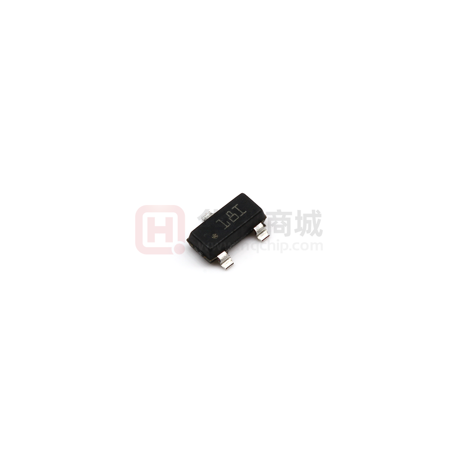
TLV76012DBZR
ACTIVE
SOT-23
DBZ
3
3000
RoHS & Green
SN
Level-1-260C-UNLIM
-40 to 125
18G
TLV76012DBZT
ACTIVE
SOT-23
DBZ
3
250
RoHS & Green
SN
Level-1-260C-UNLIM
-40 to 125
18G
TLV76015DBZR
ACTIVE
SOT-23
DBZ
3
3000
RoHS & Green
SN
Level-1-260C-UNLIM
-40 to 125
18C
TLV76015DBZT
ACTIVE
SOT-23
DBZ
3
250
RoHS & Green
SN
Level-1-260C-UNLIM
-40 to 125
18C
TLV76033DBZR
ACTIVE
SOT-23
DBZ
3
3000
RoHS & Green
SN
Level-1-260C-UNLIM
-40 to 125
18H
TLV76033DBZT
ACTIVE
SOT-23
DBZ
3
250
RoHS & Green
SN
Level-1-260C-UNLIM
-40 to 125
18H
TLV76050DBZR
ACTIVE
SOT-23
DBZ
3
3000
RoHS & Green
SN
Level-1-260C-UNLIM
-40 to 125
18I
TLV76050DBZT
ACTIVE
SOT-23
DBZ
3
250
RoHS & Green
SN
Level-1-260C-UNLIM
-40 to 125
18I
(1)
The marketing status values are defined as follows:
ACTIVE: Product device recommended for new designs.
LIFEBUY: TI has announced that the device will be discontinued, and a lifetime-buy period is in effect.
NRND: Not recommended for new designs. Device is in production to support existing customers, but TI does not recommend using this part in a new design.
PREVIEW: Device has been announced but is not in production. Samples may or may not be available.
OBSOLETE: TI has discontinued the production of the device.
(2)
RoHS: TI defines "RoHS" to mean semiconductor products that are compliant with the current EU RoHS requirements for all 10 RoHS substances, including the requirement that RoHS substance
do not exceed 0.1% by weight in homogeneous materials. Where designed to be soldered at high temperatures, "RoHS" products are suitable for use in specified lead-free processes. TI may
reference these types of products as "Pb-Free".
RoHS Exempt: TI defines "RoHS Exempt" to mean products that contain lead but are compliant with EU RoHS pursuant to a specific EU RoHS exemption.
Green: TI defines "Green" to mean the content of Chlorine (Cl) and Bromine (Br) based flame retardants meet JS709B low halogen requirements of