Product
Folder
Sample &
Buy
Support &
Community
Tools &
Software
Technical
Documents
Reference
Design
TPD2E009
SLVS953B – JUNE 2009 – REVISED AUGUST 2015
TPD2E009 2-Channel ESD Solution for High-Speed (6-Gbps) Differential Interface
1 Features
3 Description
•
•
The TPD2E009 device provides two ESD protection
diodes with flow-through pin mapping for ease of
board layout. This device has been designed to
protect sensitive components which are connected to
ultra high-speed data and transmission lines. The
TPD2E009 offers transient voltage suppression for
Level 4 of IEC 61000-4-2 Contact ESD protection.
TVS protection up to a 5-A (8/20 μs) peak pulsecurrent rating per the IEC 61000-4-5 (lightning)
specification is also provided.
1
•
•
•
•
•
•
Supports Data Rates up to 6 Gbps
IEC 61000-4-2 ESD Protection
– ±8-kV Contact Discharge
– ±8-kV Air-Gap Discharge
IEC 61000-4-5 Surge Protection
– 5 A (8/20 µs)
Low Capacitance
– DRT: 0.7-pF (Typ)
– DBZ: 0.9-pF (Typ)
0.05-pF Matching Capacitance Between the
Differential Signal Pair
Dual-Matching TVS Diodes to Protect the
Differential Data and Clock Lines of HDMI, LVDS,
SATA, Ethernet, or USB Interfaces
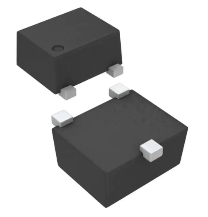
Space-Saving DRT and DBZ Package Options
Flow-Through Pin Mapping for the High-Speed
Lines Ensures Zero Additional Skew Due to Board
Layout While Placing the ESD-Protection Chip
Near the Connector
•
The TPD2E009 TVS diode is offered in a DRT
(1 mm × 0.8 mm) package for space-saving portable
applications. The industry standard DBZ (2.92 mm ×
1.3 mm) package offers additional flexibility in the
board layout for the system designer.
Typical applications for the TPD2E009 line of ESD
protection products are: HDMI, USB, eSATA, and
ethernet interfaces in notebooks, DVD and media
players, set-top boxes, and portable computers.
2 Applications
•
The monolithic silicon technology allows matching
between the differential signal pairs. The less than
0.05-pF differential capacitance ensures that the
differential signal distortion due to added ESD circuit
protection remains minimal. The low capacitance
(0.7-pF) is suitable for high-speed data rates up to
6 Gbps.
End Equipment:
– Notebooks
– Set-Top Boxes
– Portable Computers
– DVD Players
– Media Players
Interfaces:
– HDMI 2.0
– USB 3.0
– eSATA
– Ethernet
Device Information(1)
PART NUMBER
TPD2E009
PACKAGE
SOT (3)
BODY SIZE (NOM)
2.92 mm × 1.30 mm
1.00 mm × 0.80 mm
(1) For all available packages, see the orderable addendum at
the end of the data sheet.
TPD2E009 Application Curve
TPD2E009 Circuit
D–
D+
GND
1
An IMPORTANT NOTICE at the end of this data sheet addresses availability, warranty, changes, use in safety-critical applications,
intellectual property matters and other important disclaimers. PRODUCTION DATA.
�TPD2E009
SLVS953B – JUNE 2009 – REVISED AUGUST 2015
www.ti.com
Table of Contents
1
2
3
4
5
6
7
Features ..................................................................
Applications ...........................................................
Description .............................................................
Revision History.....................................................
Pin Configuration and Functions .........................
Specifications.........................................................
1
1
1
2
3
3
6.1
6.2
6.3
6.4
6.5
6.6
3
3
3
4
4
5
Absolute Maximum Ratings .....................................
ESD Ratings..............................................................
Recommended Operating Conditions.......................
Thermal Information ..................................................
Electrical Characteristics...........................................
Typical Characteristics ..............................................
Detailed Description .............................................. 6
7.1 Overview ................................................................... 6
7.2 Functional Block Diagram ......................................... 6
7.3 Feature Description................................................... 6
7.4 Device Functional Modes.......................................... 6
8
Application and Implementation .......................... 7
8.1 Application Information.............................................. 7
8.2 Typical Application ................................................... 7
9 Power Supply Recommendations........................ 9
10 Layout..................................................................... 9
10.1 Layout Guidelines ................................................... 9
10.2 Layout Examples..................................................... 9
11 Device and Documentation Support ................. 11
11.1
11.2
11.3
11.4
Community Resources..........................................
Trademarks ...........................................................
Electrostatic Discharge Caution ............................
Glossary ................................................................
11
11
11
11
12 Mechanical, Packaging, and Orderable
Information ........................................................... 11
4 Revision History
NOTE: Page numbers for previous revisions may differ from page numbers in the current version.
Changes from Revision A (June 2009) to Revision B
•
2
Page
Added Pin Configuration and Functions section, ESD Ratings table, Feature Description section, Device Functional
Modes, Application and Implementation section, Power Supply Recommendations section, Layout section, Device
and Documentation Support section, and Mechanical, Packaging, and Orderable Information section .............................. 1
Submit Documentation Feedback
Copyright © 2009–2015, Texas Instruments Incorporated
Product Folder Links: TPD2E009
�TPD2E009
www.ti.com
SLVS953B – JUNE 2009 – REVISED AUGUST 2015
5 Pin Configuration and Functions
DBZ, DRT Packages
3-Pin SOT
TOP VIEW
D+
1
3
D–
GND
2
Pin Functions
PIN
NAME
TYPE
NO.
D+
1
D–
2
GND
3
ESD port
GND
DESCRIPTION
High-speed ESD clamp provides ESD protection to the high-speed differential data lines
Ground
6 Specifications
6.1 Absolute Maximum Ratings (1)
over operating free-air temperature range (unless otherwise noted)
Operating temperature
I/O voltage tolerance
Peak pulse current (tp = 8/20 μs)
MIN
MAX
–40
85
°C
0
6
V
D+, D– pins
5
A
45
W
125
°C
Peak pulse power (tp = 8/20 μs)
Storage temperature, Tstg
(1)
–65
UNIT
Stresses beyond those listed under Absolute Maximum Ratings may cause permanent damage to the device. These are stress ratings
only, and functional operation of the device at these or any other conditions beyond those indicated in the operational sections of the
specifications is not implied. Exposure to absolute maximum-rated conditions for extended periods may affect device reliability.
6.2 ESD Ratings
VALUE
Human body model (HBM), per ANSI/ESDA/JEDEC JS-001
V(ESD)
(1)
(2)
Electrostatic
discharge
(1)
UNIT
±15000
Charged-device model (CDM), per JEDEC specification JESD22-C101 (2)
±1000
IEC 61000-4-2 contact discharge
D+, D– pins
±8000
IEC 61000-4-2 air-gap discharge
D+, D– pins
±8000
V
JEDEC document JEP155 states that 500-V HBM allows safe manufacturing with a standard ESD control process.
JEDEC document JEP157 states that 250-V CDM allows safe manufacturing with a standard ESD control process.
6.3 Recommended Operating Conditions
over operating free-air temperature range (unless otherwise noted)
MIN
Operating free-air temperature, TA
Operating voltage
Pin 1 or 2 to 3 or Pin 3 to 1 or 2
NOM
MAX
UNIT
–40
85
°C
0
5.5
V
Submit Documentation Feedback
Copyright © 2009–2015, Texas Instruments Incorporated
Product Folder Links: TPD2E009
3
�TPD2E009
SLVS953B – JUNE 2009 – REVISED AUGUST 2015
www.ti.com
6.4 Thermal Information
TPD2E009
THERMAL METRIC (1)
DBZ (SOT)
DRT (SOT)
3 PINS
3 PINS
UNIT
610
°C/W
RθJA
Junction-to-ambient thermal resistance
461.8
RθJC(top)
Junction-to-case (top) thermal resistance
216.2
288
°C/W
RθJB
Junction-to-board thermal resistance
195.6
118.4
°C/W
ψJT
Junction-to-top characterization parameter
70.1
20.2
°C/W
ψJB
Junction-to-board characterization parameter
193.7
116.4
°C/W
(1)
For more information about traditional and new thermal metrics, see the Semiconductor and IC Package Thermal Metrics application
report, SPRA953.
6.5 Electrical Characteristics
over operating free-air temperature range (unless otherwise noted)
PARAMETER
TEST CONDITIONS
VRWM
Reverse stand-off voltage
D+, D– pins to ground
VCLAMP
Clamp voltage
D+, D– pins to ground,
IIO
Current from I/O port to supply pins
VIO = 2.5 V
VD
Diode forward voltage
RDYN
Dynamic resistance
CIO
I/O capacitance
VBR
4
Break-down voltage
MIN
TYP
MAX
UNIT
5.5
V
8
V
0.01
0.1
μA
IIO = 1 A
D+, D– pins,
lower clamp diode,
VIO = 2.5 V, ID = 8 mA
0.6
0.8
0.95
D+, D– pins,
upper clamp diode,
DRY package
VCC = 0 V, ID = –8 mA
0.6
0.8
0.95
D+, D– pins,
I=1A
D+, D– pins, DBZ
Package
D+, D– pins, DRT
Package
V
1
Ω
VIO = 2.5 V, f = 10 MHz
0.9
pF
VIO = 2.5 V, f = 10 MHz
0.7
pF
IIO = 1 mA
Submit Documentation Feedback
7
V
Copyright © 2009–2015, Texas Instruments Incorporated
Product Folder Links: TPD2E009
�TPD2E009
www.ti.com
SLVS953B – JUNE 2009 – REVISED AUGUST 2015
6.6 Typical Characteristics
10
1.2x10⁻¹²
DBZ
DRT
1.1x10⁻¹²
5
Leakage Current (pA)
0
Capacitance (F)
1x10-12
900x10-15
800x10-15
700x10-15
-5
-10
-15
-20
-25
-30
600x10-15
-40
-40
500x10
0
0.5
1
1.5
2
2.5
3
Voltage (V)
3.5
4
4.5
5
Figure 1. I/O Capacitance vs I/O Voltage (TA= 25°C)
6
5
60
Current (A) 55
Power (W)
50
4.5
45
30
2.5
25
2
20
1.5
15
4
1
10
3
15
20
25
30
Time (µs)
35
40
45
0
50
PPP (W)
3
10
80
D001
9
40
5
60
8
35
0
20
40
Temperature (°C)
10
4
5
0
11
3.5
0.5
-20
Figure 2. Leakage Current vs Temperature (VIO = 2.5 V)
Current (A)
IPP (A)
5.5
0
D+
D-
-35
-15
7
6
5
2
1
0
0
5
20
90
10
80
0
70
-10
60
-20
Amplitude (V)
Amplitude (V)
100
40
30
20
-80
-90
-20
-100
100
125
Time (nS)
150
175
200
Figure 5. IEC Clamping Waveforms (8-kV Contact)
35
40
-60
-10
75
30
-50
-70
50
25
-40
0
25
20
Voltage (V)
-30
10
0
15
Figure 4. D+, D– Transmission Line Pulser Plot
(100-ns Pulse, 10-ns Rise Time)
Figure 3. Peak Pulse Waveforms,
(Measured at One I/O, With the Other I/O Open)
50
10
0
25
50
75
100
125
Time (nS)
150
175
200
Figure 6. IEC Clamping Waveforms (–8-kV Contact)
Submit Documentation Feedback
Copyright © 2009–2015, Texas Instruments Incorporated
Product Folder Links: TPD2E009
5
�TPD2E009
SLVS953B – JUNE 2009 – REVISED AUGUST 2015
www.ti.com
7 Detailed Description
7.1 Overview
TPD2E009 is a two-channel ESD TVS that provides ±8-kV IEC 61000-4-2 contact and air-gap ESD protection.
The 0.7-pF unidirectional diode architecture is suitable for signals that range from 0 V to 5.5 V and can support
data rates up to 6 Gbps. The industry-standard packages are convenient for placement in applications with
limited space.
7.2 Functional Block Diagram
D–
D+
GND
7.3 Feature Description
TPD2E009 is a unidirectional TVS offering IEC 61000-4-2 Level 4 Contact ESD protection. This device protects
circuits from ESD strikes up to ±8-kV contact and ±8-kV air-gap. The device can also handle up to 5-A surge
current (IEC 61000-4-5 8/20 μs). The low capacitance of 0.7 pF supports a data rate up to 6 Gbps. TPD2E009
has a small dynamic resistance of 1 Ω, which makes the clamping voltage low when the device is actively
protecting other circuits. For example, the clamping voltage is only 8 V when the device is taking a 1-A transient
current. Low leakage allows the diode to conserve power when working below the VRWM.
7.4 Device Functional Modes
The TPD2E009 device is a passive clamp that has low leakage during normal operation when the voltage
between an I/O pin and GND is below VRWM. The device activates when the voltage is between an I/O pin and
GND goes above VBR. During ESD events, transient voltages as high as ±8 kV can be clamped between the
protected line and ground. When the voltages on the protected lines fall below the trigger voltage, the device
reverts back to the low-leakage passive state.
6
Submit Documentation Feedback
Copyright © 2009–2015, Texas Instruments Incorporated
Product Folder Links: TPD2E009
�TPD2E009
www.ti.com
SLVS953B – JUNE 2009 – REVISED AUGUST 2015
8 Application and Implementation
NOTE
Information in the following applications sections is not part of the TI component
specification, and TI does not warrant its accuracy or completeness. TI’s customers are
responsible for determining suitability of components for their purposes. Customers should
validate and test their design implementation to confirm system functionality.
8.1 Application Information
The TPD2E009 device is a diode-array type TVS typically used to provide a path to ground for dissipating ESD
events on high-speed signal lines between a human-interface connector and a system. As the current from ESD
passes through the TVS, only a small voltage drop is present across the diode. This is the voltage presented to
the protected IC. The low RDYN of the triggered TVS holds this voltage, VCLAMP, to a tolerable level to the
protected IC.
8.2 Typical Application
The TPD2E009 device is typically used to protect a single high-speed differential pair. Multiple TPD2E009
devices can be used to provide protection for connectors with multiple differential data lanes. This example is
applicable to many interface types including:
• HDMI
• USB
• eSATA
• ethernet interfaces
D+
D+
D-
DD+
Core
Chip
High-Speed
Interface
D-
TPD2E009
D+
D-
TPD2E009
Figure 7. TPD2E009 in a High-Speed Interface
8.2.1 Design Requirements
For this design example, TPD2E009 is used to protect any differential data pair meeting the design requirements
shown in the following table.
DESIGN PARAMETER
VALUE
Maximum signal range on D+ and D–
0 V to 5.5 V
Maximum Operating Frequency
3 GHz
8.2.2 Detailed Design Procedure
To begin the design process, some parameters must be decided upon; the designer must know the following:
• The signal voltage range on the protected lines
• The maximum operating frequency
Submit Documentation Feedback
Copyright © 2009–2015, Texas Instruments Incorporated
Product Folder Links: TPD2E009
7
�TPD2E009
SLVS953B – JUNE 2009 – REVISED AUGUST 2015
www.ti.com
8.2.3 Application Curves
8
Figure 8. Eye Diagram With TPD2E009
(3.3-Gbps Data Rate)
(3-Pin DBZ Package)
Figure 9. Eye Diagram Without TPD2E009
(3.3-Gbps Data Rate)
(3-Pin DBZ Package)
Figure 10. Eye Diagram With TPD2E009
(5-Gbps Data Rate)
(3-Pin DBZ Package)
Figure 11. Eye Diagram Without TPD2E009
(5-Gbps Data Rate)
(3-Pin DBZ Package)
Figure 12. Eye Diagram With TPD2E009
(6-Gbps Data Rate)
(3-Pin DBZ Package)
Figure 13. Eye Diagram Without TPD2E009
(6-Gbps Data Rate)
(3-Pin DBZ Package)
Submit Documentation Feedback
Copyright © 2009–2015, Texas Instruments Incorporated
Product Folder Links: TPD2E009
�TPD2E009
www.ti.com
SLVS953B – JUNE 2009 – REVISED AUGUST 2015
9 Power Supply Recommendations
The TPD2E009 device is a passive ESD-protection device, and therefore, does not require a power supply. Care
must be taken to avoid violating the maximum-voltage specification to ensure that the device functions properly.
The D+ and D– lines share a TVS diode that can tolerate up to 5.5 V.
10 Layout
10.1 Layout Guidelines
Layout considerations such as package selection, trace routing, and so forth, must be accounted for while
designing the ESD clamp circuit for a high-speed interface. Difficult routing can lead the designer to use vias or
stubs in the board traces, which creates significant disruption in the line impedance in the high-speed signal path.
Poor package choice can force the designer to route differential traces with unequal lengths and add the skew in
the signals. TI recommends coupling the differential traces closely to reduce the EMI interference.
The TPD2E009 can provide system-level ESD protection to the high-speed differential ports (up to 6-Gbps data
rate). The flow-through package offers flexibility for board routing with traces up to 15 mils (0.38 mm) wide.
Figure 14 and Figure 15 show the board layout scheme for the D+ and D– lines of a single differential pair, which
allows the differential signal pairs to couple together right after they touch the ESD ports (pin 1 and pin 2) of the
TPD2E009.
10.2 Layout Examples
1.27 mm
1.27 mm
BOARD LAYOUT
FOR DRT PACKAGE
TPD2E009DRTR AT
eSATA PORT
D+
GND
D–
GND VIA
Figure 14. TPD2E009DRTR at eSATA Connector Interface
Submit Documentation Feedback
Copyright © 2009–2015, Texas Instruments Incorporated
Product Folder Links: TPD2E009
9
�TPD2E009
SLVS953B – JUNE 2009 – REVISED AUGUST 2015
www.ti.com
Layout Examples (continued)
1.27 mm
1.27 mm
BOARD LAYOUT
FOR DBZ PACKAGE
TPD2E009DBZR AT
eSATA PORT
D+
GND
D–
GND VIA
Figure 15. TPD2E009DBZR at eSATA Connector Interface
10
Submit Documentation Feedback
Copyright © 2009–2015, Texas Instruments Incorporated
Product Folder Links: TPD2E009
�TPD2E009
www.ti.com
SLVS953B – JUNE 2009 – REVISED AUGUST 2015
11 Device and Documentation Support
11.1 Community Resources
The following links connect to TI community resources. Linked contents are provided "AS IS" by the respective
contributors. They do not constitute TI specifications and do not necessarily reflect TI's views; see TI's Terms of
Use.
TI E2E™ Online Community TI's Engineer-to-Engineer (E2E) Community. Created to foster collaboration
among engineers. At e2e.ti.com, you can ask questions, share knowledge, explore ideas and help
solve problems with fellow engineers.
Design Support TI's Design Support Quickly find helpful E2E forums along with design support tools and
contact information for technical support.
11.2 Trademarks
E2E is a trademark of Texas Instruments.
All other trademarks are the property of their respective owners.
11.3 Electrostatic Discharge Caution
These devices have limited built-in ESD protection. The leads should be shorted together or the device placed in conductive foam
during storage or handling to prevent electrostatic damage to the MOS gates.
11.4 Glossary
SLYZ022 — TI Glossary.
This glossary lists and explains terms, acronyms, and definitions.
12 Mechanical, Packaging, and Orderable Information
The following pages include mechanical, packaging, and orderable information. This information is the most
current data available for the designated devices. This data is subject to change without notice and revision of
this document. For browser-based versions of this data sheet, refer to the left-hand navigation.
Submit Documentation Feedback
Copyright © 2009–2015, Texas Instruments Incorporated
Product Folder Links: TPD2E009
11
�PACKAGE OPTION ADDENDUM
www.ti.com
10-Dec-2020
PACKAGING INFORMATION
Orderable Device
Status
(1)
Package Type Package Pins Package
Drawing
Qty
Eco Plan
(2)
Lead finish/
Ball material
MSL Peak Temp
Op Temp (°C)
Device Marking
(3)
(4/5)
(6)
TPD2E009DBZR
ACTIVE
SOT-23
DBZ
3
3000
RoHS & Green NIPDAU | NIPDAUAG
Level-1-260C-UNLIM
-40 to 85
(NFLO, NFLR)
TPD2E009DRTR
ACTIVE
SOT-9X3
DRT
3
3000
RoHS & Green
Level-1-260C-UNLIM
-40 to 85
4T
NIPDAU
(1)
The marketing status values are defined as follows:
ACTIVE: Product device recommended for new designs.
LIFEBUY: TI has announced that the device will be discontinued, and a lifetime-buy period is in effect.
NRND: Not recommended for new designs. Device is in production to support existing customers, but TI does not recommend using this part in a new design.
PREVIEW: Device has been announced but is not in production. Samples may or may not be available.
OBSOLETE: TI has discontinued the production of the device.
(2)
RoHS: TI defines "RoHS" to mean semiconductor products that are compliant with the current EU RoHS requirements for all 10 RoHS substances, including the requirement that RoHS substance
do not exceed 0.1% by weight in homogeneous materials. Where designed to be soldered at high temperatures, "RoHS" products are suitable for use in specified lead-free processes. TI may
reference these types of products as "Pb-Free".
RoHS Exempt: TI defines "RoHS Exempt" to mean products that contain lead but are compliant with EU RoHS pursuant to a specific EU RoHS exemption.
Green: TI defines "Green" to mean the content of Chlorine (Cl) and Bromine (Br) based flame retardants meet JS709B low halogen requirements of