Product
Folder
Sample &
Buy
Support &
Community
Tools &
Software
Technical
Documents
TPD8S009
SLVS816A – JULY 2008 – REVISED DECEMBER 2015
TPD8S009 8-Channel ESD Protection for DisplayPort and HDMI
1 Features
3 Description
•
The TPD8S009 device is an eight-channel TVS diode
array for ESD protection. The TPD8S009 is rated to
dissipate contact ESD strikes at the maximum level
specified in the IEC 61000-4-2 international standard
(Level 4), with ±8-kV contact discharge ESD
protection. The low capacitance (0.8 pF) of this
device, coupled with the excellent matching between
differential signal pairs enables this device to provide
transient voltage suppression circuit protection for
high-speed idfferential data rates (3-dB bandwidth >
4 GHz).
1
•
•
•
•
•
•
•
IEC 61000-4-2 Level 4 ESD Protection
– ±8-kV Contact Discharge
IEC 61000-4-5 Surge Protection
– 2.5 A (8 / 20 µs)
I/O Capacitance: 0.8 pF (Typical)
Low Leakage Current: 10 nA (Typical)
Supports High-Speed Differential Data Rates
(3-dB Bandwidth > 4 GHz)
Ioff Feature
Industrial Temperature Range:
–40°C to +85°C
Easy Straight-Through Routing Package for
HDMI and DisplayPort Connectors
The TPD8S009 is offered in a 8-pin SON package.
This package offers easy design and layout, as the
package matches exactly with the HDMI and
DisplayPort high-speed pinout.
Device Information(1)
2 Applications
•
•
PART NUMBER
End Equipment
– Set-Top Boxes
– Laptops and Desktops
– Projectors
– Video Surveillance
Interfaces
– DisplayPort 1.1
– HDMI 1.4
– DVI
TPD8S009
PACKAGE
SON (15)
BODY SIZE (NOM)
2.50 mm × 6.50 mm
(1) For all available packages, see the orderable addendum at
the end of the data sheet.
Simplified Internal Schematic
VCC
GND
D3–
D3+
D2–
D2+
D1–
D1+
D0–
D0+
GND
1
An IMPORTANT NOTICE at the end of this data sheet addresses availability, warranty, changes, use in safety-critical applications,
intellectual property matters and other important disclaimers. PRODUCTION DATA.
�TPD8S009
SLVS816A – JULY 2008 – REVISED DECEMBER 2015
www.ti.com
Table of Contents
1
2
3
4
5
6
7
Features ..................................................................
Applications ...........................................................
Description .............................................................
Revision History.....................................................
Pin Configuration and Functions .........................
Specifications.........................................................
1
1
1
2
3
4
6.1
6.2
6.3
6.4
6.5
6.6
4
4
4
4
5
5
Absolute Maximum Ratings ......................................
ESD Ratings..............................................................
Recommended Operating Conditions.......................
Thermal Information ..................................................
Electrical Characteristics...........................................
Typical Characteristics ..............................................
Detailed Description .............................................. 6
7.1 Overview ................................................................... 6
7.2 Functional Block Diagram ......................................... 6
7.3 Feature Description................................................... 6
7.4 Device Functional Modes.......................................... 7
8
Application and Implementation .......................... 8
8.1 Application Information.............................................. 8
8.2 Typical Application ................................................... 8
9 Power Supply Recommendations...................... 10
10 Layout................................................................... 10
10.1 Layout Guidelines ................................................. 10
10.2 Layout Example .................................................... 10
11 Device and Documentation Support ................. 11
11.1
11.2
11.3
11.4
Community Resources..........................................
Trademarks ...........................................................
Electrostatic Discharge Caution ............................
Glossary ................................................................
11
11
11
11
12 Mechanical, Packaging, and Orderable
Information ........................................................... 11
4 Revision History
NOTE: Page numbers for previous revisions may differ from page numbers in the current version.
Changes from Original (July 2008) to Revision A
Page
•
Added ESD Ratings table, Feature Description section, Device Functional Modes, Application and Implementation
section, Power Supply Recommendations section, Layout section, Device and Documentation Support section, and
Mechanical, Packaging, and Orderable Information section. ................................................................................................. 1
•
Deleted Ordering Information table ........................................................................................................................................ 1
•
Removed Lead temperature from Absolute Maximum Ratings ............................................................................................. 4
2
Submit Documentation Feedback
Copyright © 2008–2015, Texas Instruments Incorporated
Product Folder Links: TPD8S009
�TPD8S009
www.ti.com
SLVS816A – JULY 2008 – REVISED DECEMBER 2015
5 Pin Configuration and Functions
DSM Package
15-Pin SON
Top View
D0+
1
GND
2
D0–
3
D1+
4
GND
5
D1–
6
D2+
7
GND
8
D2–
9
D3+
10
GND
11
D3–
12
15
VCC
14
N.C.
13
VCC
N.C. – Not internally connected
Pin Functions
PIN
NO.
NAME
1
D0+
3
D0–
4
D1+
6
D1–
7
D2+
9
D2–
10
D3+
12
D3–
TYPE
ESD port
DESCRIPTION
High-speed ESD clamp provides ESD protection to the high-speed display port/HDMI
differential data lines.
2
5
8
GND
GND
N.C.
No connect
VCC
Supply
Ground
11
14
13
15
No internal signal connection
I/O supply
Submit Documentation Feedback
Copyright © 2008–2015, Texas Instruments Incorporated
Product Folder Links: TPD8S009
3
�TPD8S009
SLVS816A – JULY 2008 – REVISED DECEMBER 2015
www.ti.com
6 Specifications
6.1 Absolute Maximum Ratings
over operating free-air temperature range (unless otherwise noted) (1)
VCC
Supply voltage
VIO
IO signal voltage
TA
Characterized free-air operating temperature
PPP
Peak pulse power (tp = 8/20 μs)
IPP
Peak pulse current (tp = 8/20 μs)
Tstg
Storage temperature
(1)
MIN
MAX
UNIT
–0.3
6
V
0
VCC
V
–40
85
°C
25
W
–65
2.5
A
125
°C
Stresses beyond those listed under Absolute Maximum Ratings may cause permanent damage to the device. These are stress ratings
only, which do not imply functional operation of the device at these or any other conditions beyond those indicated under Recommended
Operating Conditions. Exposure to absolute-maximum-rated conditions for extended periods may affect device reliability.
6.2 ESD Ratings
VALUE
V(ESD)
(1)
(2)
Electrostatic discharge
Human-body model (HBM), per ANSI/ESDA/JEDEC JS-001 (1)
±2500
Charged-device model (CDM), per JEDEC specification JESD22C101 (2)
±1000
IEC 61000-4-2 Contact Discharge
±8000
IEC 61000-4-2 Air-Gap Discharge
±9000
UNIT
V
JEDEC document JEP155 states that 500-V HBM allows safe manufacturing with a standard ESD control process.
JEDEC document JEP157 states that 250-V CDM allows safe manufacturing with a standard ESD control process.
6.3 Recommended Operating Conditions
over operating free-air temperature range (unless otherwise noted)
VIO
Input pin voltage
TA
Operating free-air temperature
MIN
MAX
UNIT
0
VCC
V
–40
85
°C
6.4 Thermal Information
TPD8S009
THERMAL METRIC (1)
DSM (SON)
UNIT
15 PINS
RθJA
Junction-to-ambient thermal resistance
405.4
°C/W
RθJC(top)
Junction-to-case (top) thermal resistance
35.4
°C/W
RθJB
Junction-to-board thermal resistance
284.3
°C/W
ψJT
Junction-to-top characterization parameter
49.2
°C/W
ψJB
Junction-to-board characterization parameter
284.3
°C/W
RθJC(bot)
Junction-to-case (bottom) thermal resistance
n/a
°C/W
(1)
4
For more information about traditional and new thermal metrics, see the Semiconductor and IC Package Thermal Metrics application
report, SPRA953.
Submit Documentation Feedback
Copyright © 2008–2015, Texas Instruments Incorporated
Product Folder Links: TPD8S009
�TPD8S009
www.ti.com
SLVS816A – JULY 2008 – REVISED DECEMBER 2015
6.5 Electrical Characteristics
over operating free-air temperature range (unless otherwise noted)
PARAMETER
TEST CONDITIONS
MIN
TYP
MAX
UNIT
VRWM
Reverse standoff voltage
Any IO pin to ground
VBR
Breakdown voltage
IIO = 1 mA
Any IO pin to ground
5.5
V
IIO
IO port current
VIO = 3.3 V, VCC = 5 V
Any IO pin
0.01
0.1
μA
Ioff
Current from IO port to supply pins
VIO = 3.3 V, VCC = 5 V
Any IO pin
0.01
0.1
μA
VD
Diode forward voltage
IIO = 8 mA
Lower clamp diode
RDYN
Dynamic resistance
I=1A
Any IO pin
0.8
1.1
0.95
Ω
CIO
IO capacitance
VCC = 5 V, VIO = 2.5 V
Any IO pin
0.8
pF
ICC
Operating supply current
VIO = Open, VCC = 5 V
VCC pin
0.1
9
V
0.6
V
μA
1
6.6 Typical Characteristics
1
4.0
48
0
3.5
42
–1
36
3.0
–3
D0D1+
–4
D1-
2.5
30
2.0
24
D2+
–5
D2-
PPP (W)
Power (W)
D0+
IPP (A)
Insertion Loss (dB)
–2
18
1.5
–6
Current (A)
–7
–8
–9
1.0E+00
1.0E+02
1.0E+04
1.0E+06
Frequency (Hz)
1.0E+08
1.0E+10
1.0
12
0.5
6
5
0
10
Figure 1. Insertion Loss vs Frequency
15
20
25
30
Time (μs)
35
40
45
Figure 2. Peak Pulse Waveforms
240
80
200
40
160
0
120
–40
Amplitude (V)
Amplitude (V)
0
50
0.0
80
–80
40
–120
0
–160
–40
–200
–80
–240
0
20
40
60
80
100
120
Time (ns)
140
160
180
Figure 3. IEC Clamping Waveforms
(8-kV Contact)
200
0
20
40
60
80
100
120
Time (ns)
140
160
180
200
Figure 4. Figure 3. IEC Clamping Waveforms
(–8-kV Contact)
Submit Documentation Feedback
Copyright © 2008–2015, Texas Instruments Incorporated
Product Folder Links: TPD8S009
5
�TPD8S009
SLVS816A – JULY 2008 – REVISED DECEMBER 2015
www.ti.com
7 Detailed Description
7.1 Overview
The TPD8S009 is an eight-channel TVS diode array for ESD protection. TPD8S009 is rated to dissipate contact
ESD strikes at the maximum level specified in the IEC 61000-4-2 international standard (Level 4), with ±8-kV
contact discharge ESD protection. The low capacitance (0.8 pF) of this device, coupled with the excellent
matching between differential signal pairs enables this device to provide transient voltage suppression circuit
protection for high-speed idfferential data rates (3-dB bandwidth > 4 GHz).
The TPD8S009 offers an optional VCC supply pin which can be connected to system supply plane. There is a
blocking diode at the VCC pin to enable the Ioff feature for the TPD8S009. The TPD8S009 can handle live signal
at the signal pins when the VCC pin is connected to 0 V. The VCC pin allows all the internal circuit nodes of the
TPD8S009 to be at known potential during start-up time. However, connecting the optional VCC pin to board
supply plane doesn't affect the system level ESD performance of the TPD8S009.
7.2 Functional Block Diagram
VCC
GND
D3–
D3+
D2–
D2+
D1–
D1+
D0–
D0+
GND
7.3 Feature Description
7.3.1 IEC 61000-4-2 ESD Protection
The I/O pins can withstand ESD events up to ±8-kV contact and ±9-kV air. An ESD and surge clamp diverts the
current to ground.
7.3.2 IEC 61000-4-5 Surge Protection
The I/O pins can withstand surge events up to 2.5 A and 25 W (8/20-µs waveform). An ESD and surge clamp
diverts this current to ground.
7.3.3 I/O Capacitance
The capacitance between each I/O pin to ground is 0.8 pF (typical). This device can support data rates up to
3.4 Gbps.
7.3.4 Low Leakage Current
The I/O pins feature a low leakage current of 10 nA (typical) with an IO bias of 3.3 V and VCC bias of 5 V.
7.3.5 Supports High-Speed Differential Data Rates
The I/O pins low capacitance of 0.8 pF (typical) gives them a typical –3-dB bandwidth > 4 GHz. This allows the
TPD8S009 to protect interfaces with high-speed signals like HDMI 1.4.
6
Submit Documentation Feedback
Copyright © 2008–2015, Texas Instruments Incorporated
Product Folder Links: TPD8S009
�TPD8S009
www.ti.com
SLVS816A – JULY 2008 – REVISED DECEMBER 2015
Feature Description (continued)
7.3.6 Ioff Feature
The TPD8S009 offers an optional VCC supply pin which can be connected to system supply plane. There is a
blocking diode at the VCC pin which makes it so the TPD4S009 can handle live signal at the D+, D– pins when
the VCC pin is connected to 0 V. This is the Ioff feature, which is crucial for HDMI, as a live signal can be put on
the IO pins when the system is powered off.
7.3.7 Industrial Temperature Range
This device features an industrial operating range of –40°C to +85°C.
7.3.8 Easy Straight Through Routing
The layout of this device makes it simple and easy to add protection to an existing layout. The packages offers
flow-through routing, requiring minimal modification to an existing layout. Flow-through routing also allows the
PCB designer to optimize the signal integrity of any high-speed signals being protected.
7.4 Device Functional Modes
TPD8S009 is a passive-integrated circuit that activates whenever voltages above VBR or below the lower diodes
Vforward (–0.6 V) are present upon the circuit being protected. During ESD events, voltages as high as ±9 kV can
be directed to ground and VCC through the internal diode network. Once the voltages on the protected lines fall
below the trigger voltage of the TPD8S009 (usually within 10's of nano-seconds) the device reverts back to a
high-impedance state.
Submit Documentation Feedback
Copyright © 2008–2015, Texas Instruments Incorporated
Product Folder Links: TPD8S009
7
�TPD8S009
SLVS816A – JULY 2008 – REVISED DECEMBER 2015
www.ti.com
8 Application and Implementation
NOTE
Information in the following applications sections is not part of the TI component
specification, and TI does not warrant its accuracy or completeness. TI’s customers are
responsible for determining suitability of components for their purposes. Customers should
validate and test their design implementation to confirm system functionality.
8.1 Application Information
The TPD8S009 can provide system-level ESD protection to the high-speed differential lines of the HDMI or
display ports. The flow-through package offers flexibility for board routing with traces up to 15-mm wide. Figure 5
shows the board-layout scheme for the four differential pair lines. The special pin configuration of the TPD8S009
matches the HDMI or DisplayPort pin assignments. It allows the differential signal pairs to couple together after
they touch the ESD ports (pins 1–3, 4–6, 7–9, and 10–12) of the TPD8S009.
The TPD4E001 is recommended for ESD protection of slow-speed control lines.
8.2 Typical Application
PIN NO.
SIGNAL
TYPE
1
Out
2
GND
3
PIN NAME
MATING
ROW
CONTACT
LOCATION
ML Lane 0(p)
Top
GND
Bottom
Out
ML Lane 0(n)
Top
4
Out
ML Lane 1(p)
Bottom
8
GND
GND
Top
6
Out
ML Lane 1(n)
Bottom
7
Out
ML Lane 2(p)
Top
8
GND
GND
Bottom
9
Out
ML Lane 2(n)
Top
10
Out
ML Lane 3(p)
Bottom
11
GND
GND
Top
12
Out
ML Lane 3(n)
Bottom
13
GND
GND
Top
14
GND
GND
Bottom
15
I/O
Aux CH (p)
Top
16
GND
GND
Bottom
17
I/O
Aux CH (n)
Top
18
In
Hot Plug Detect
Bottom
VERTICALLY
OPPOSED
CONNECTOR
FRONT VIEW
TPD8S009
Core Scalar/
Switch
TPD4E001
19
PWR Out Return DP PWR
Top
20
PWR RIN DP PWR
Bottom
Display Port Connector
TPD8S009 and TPD4E001 provide complete ESD protection for display or HDMI interface
Figure 5. Typical Application
8
Submit Documentation Feedback
Copyright © 2008–2015, Texas Instruments Incorporated
Product Folder Links: TPD8S009
�TPD8S009
www.ti.com
SLVS816A – JULY 2008 – REVISED DECEMBER 2015
Typical Application (continued)
8.2.1 Design Requirements
For this design example, one TPD8S009 devices, and one TPD4E001 are being used in an HDMI 1.4
application. This provides a complete port protection scheme.
Given the HDMI 1.4 application, the following parameters are shown in Table 1.
Table 1. Design Parameters
DESIGN PARAMETER
VALUE
Signal range on high-speed TMDS
pins
0 V to 3.6 V
Operating Frequency
1.7 GHz
8.2.2 Detailed Design Procedure
To begin the design process, some parameters must be decided upon; the designer must know the following:
• Signal range on all the protected lines
• Operating frequency
8.2.2.1 Signal Range on High Speed TMDS Pins
TPD8S009 has 8 identical protection channels for signal lines. The symmetry of the device provides flexibility
when selecting which of the 8 I/O channels protect which signal lines. The package is also designed to easily lay
out on an HDMI connector, eliminating any tricky routing issues. Any I/O supports a signal range of 0 to 5.5 V.
Therefore, this device supports the HDMI 1.4 signal swing.
8.2.2.2 Bandwidth on High-Speed TMDS Pins
Each pin of the TPD8S009 has a typical –3-dB bandwidth of 4GHz. Therefore, this device can handle HDMI 1.4
data rate of 3.4 Gbps with operating frequency of 1.7 GHz.
8.2.3 Application Curves
Figure 6. Eye Diagram Without TPD8S009
(2.5-Gbps Data Rate)
Figure 7. Eye Diagram With TPD8S009
(2.5-Gbps Data Rate)
Submit Documentation Feedback
Copyright © 2008–2015, Texas Instruments Incorporated
Product Folder Links: TPD8S009
9
�TPD8S009
SLVS816A – JULY 2008 – REVISED DECEMBER 2015
www.ti.com
9 Power Supply Recommendations
This device is a passive ESD protection device so there is no need to power it. Take care to make sure that the
maximum voltage specifications for each pin are not violated.
10 Layout
10.1 Layout Guidelines
•
•
•
The optimum placement is as close to the connector as possible.
– EMI during an ESD event can couple from the trace being struck to other nearby unprotected traces,
resulting in early system failures.
– The PCB designer must minimize the possibility of EMI coupling by keeping any unprotected traces away
from the protected traces which are between the TVS and the connector.
Route the protected traces as straight as possible.
Eliminate any sharp corners on the protected traces between the TVS and the connector by using rounded
corners with the largest radii possible.
– Electric fields tend to build up on corners, increasing EMI coupling.
10.2 Layout Example
TPD8S009
To HDMI Connector
To HDMI Core Chip
Legend
VIA to 5V Plane
VIA to GND Plane
Figure 8. Typical Layout for HDMI Connector
10
Submit Documentation Feedback
Copyright © 2008–2015, Texas Instruments Incorporated
Product Folder Links: TPD8S009
�TPD8S009
www.ti.com
SLVS816A – JULY 2008 – REVISED DECEMBER 2015
11 Device and Documentation Support
11.1 Community Resources
The following links connect to TI community resources. Linked contents are provided "AS IS" by the respective
contributors. They do not constitute TI specifications and do not necessarily reflect TI's views; see TI's Terms of
Use.
TI E2E™ Online Community TI's Engineer-to-Engineer (E2E) Community. Created to foster collaboration
among engineers. At e2e.ti.com, you can ask questions, share knowledge, explore ideas and help
solve problems with fellow engineers.
Design Support TI's Design Support Quickly find helpful E2E forums along with design support tools and
contact information for technical support.
11.2 Trademarks
E2E is a trademark of Texas Instruments.
All other trademarks are the property of their respective owners.
11.3 Electrostatic Discharge Caution
These devices have limited built-in ESD protection. The leads should be shorted together or the device placed in conductive foam
during storage or handling to prevent electrostatic damage to the MOS gates.
11.4 Glossary
SLYZ022 — TI Glossary.
This glossary lists and explains terms, acronyms, and definitions.
12 Mechanical, Packaging, and Orderable Information
The following pages include mechanical, packaging, and orderable information. This information is the most
current data available for the designated devices. This data is subject to change without notice and revision of
this document. For browser-based versions of this data sheet, refer to the left-hand navigation.
Submit Documentation Feedback
Copyright © 2008–2015, Texas Instruments Incorporated
Product Folder Links: TPD8S009
11
�PACKAGE OPTION ADDENDUM
www.ti.com
10-Dec-2020
PACKAGING INFORMATION
Orderable Device
Status
(1)
Package Type Package Pins Package
Drawing
Qty
Eco Plan
(2)
Lead finish/
Ball material
MSL Peak Temp
Op Temp (°C)
Device Marking
(3)
(4/5)
(6)
TPD8S009DSMR
ACTIVE
SON
DSM
15
3000
RoHS & Green
NIPDAUAG
Level-1-260C-UNLIM
-40 to 85
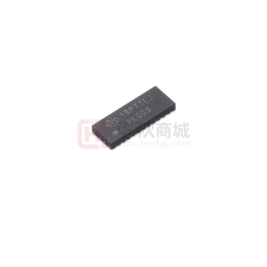
PK009
(1)
The marketing status values are defined as follows:
ACTIVE: Product device recommended for new designs.
LIFEBUY: TI has announced that the device will be discontinued, and a lifetime-buy period is in effect.
NRND: Not recommended for new designs. Device is in production to support existing customers, but TI does not recommend using this part in a new design.
PREVIEW: Device has been announced but is not in production. Samples may or may not be available.
OBSOLETE: TI has discontinued the production of the device.
(2)
RoHS: TI defines "RoHS" to mean semiconductor products that are compliant with the current EU RoHS requirements for all 10 RoHS substances, including the requirement that RoHS substance
do not exceed 0.1% by weight in homogeneous materials. Where designed to be soldered at high temperatures, "RoHS" products are suitable for use in specified lead-free processes. TI may
reference these types of products as "Pb-Free".
RoHS Exempt: TI defines "RoHS Exempt" to mean products that contain lead but are compliant with EU RoHS pursuant to a specific EU RoHS exemption.
Green: TI defines "Green" to mean the content of Chlorine (Cl) and Bromine (Br) based flame retardants meet JS709B low halogen requirements of


 工商网监
湘ICP备2023018690号
工商网监
湘ICP备2023018690号
