Sample &
Buy
Product
Folder
Technical
Documents
Support &
Community
Tools &
Software
TPS22968-Q1
SLVSCP7B – NOVEMBER 2014 – REVISED MARCH 2016
TPS22968x-Q1 5.5-V, 4-A, 27-mΩ On-Resistance Load Switch
1 Features
2 Applications
•
•
•
•
•
•
1
•
•
•
•
•
•
•
•
•
•
•
•
Integrated Dual Channel Load Switch
Qualified for Automotive Applications:
– Device Temperature Grade 1 : –40°C to
+125°C Ambient Operating Temperature
Range
Input Voltage Range: 0.8 to 5.5 V
VBIAS Voltage Range: 2.5 to 5.5 V
On-Resistance
– RON = 29 mΩ at VIN = 5 V (VBIAS = 5 V)
– RON = 27 mΩ at VIN = 3.3 V (VBIAS = 5 V)
– RON = 26 mΩ at VIN = 1.8 V (VBIAS = 5 V)
4-A Maximum Continuous Switch Current per
Channel
Low Quiescent Current
– 58-µA at VBIAS = 5 V (Both Channels)
Low-Control Input-Threshold Enables Use of 1.2-,
1.8-, 2.5-, 3.3- V Logic
Configurable Rise Time With CT Pin(1)
Quick-Output Discharge (QOD)(2) (TPS22968-Q1
Only)
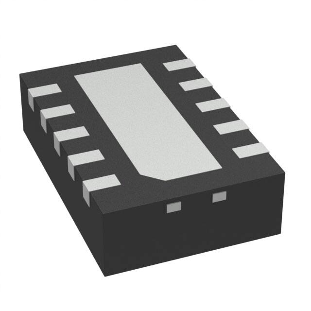
10-Pin WSON Package With Wettable Flanks
ESD Performance Tested per JEDEC STD
– ±2-kV HBM and ±1-kV CDM
Latch-Up Performance meets 100-mA per JESD
78, Class II
GPIO Enable – Active High
(1)
See Adjustable Rise Time for CT value versus rise time
(2)
This feature discharges output of the switch to GND through a
270-Ω resistor, preventing the output from floating.
Automotive Electronics
Infotainment
Cluster
ADAS
3 Description
The TPS22968x-Q1 is a small, dual-channel load
switch with configurable rise time. The device
contains two N-channel MOSFETs that can operate
over an input voltage range of 0.8 V to 5.5 V and can
support a maximum continuous current of 4-A per
channel. Each switch is independently controlled by
an on/off input (ON1 and ON2), which is capable of
interfacing directly with low-voltage control signals.
The TPS22968-Q1 includes a 270 Ω on-chip resistor
for quick output discharge when the switch is turned
off.
The TPS22968x-Q1 is available in a small, spacesaving package (DMG) with wettable flanks and an
integrated thermal pad. The wettable flanks allow for
visual solder inspection. The device is characterized
for operation over the free-air temperature range of
–40 to +125°C.
Device Information (1)
PART NUMBER
TPS22968-Q1
TPS22968N-Q1
PACKAGE
WSON (10)
BODY SIZE (NOM)
2.00 mm × 3.00 mm
(1) For all available packages, see the orderable addendum at
the end of the data sheet.
Typical Application Schematic
VIN1
C IN
ON
VOUT1
ON1
CL
Dual
Power
Supply
or
DC/DC
Converter
RL
CT1
OFF
CT2
GND
VBIAS
VIN2
C IN
ON
VOUT2
ON2
CL
RL
OFF
TPS22968x-Q1
GND
GND
1
An IMPORTANT NOTICE at the end of this data sheet addresses availability, warranty, changes, use in safety-critical applications,
intellectual property matters and other important disclaimers. PRODUCTION DATA.
�TPS22968-Q1
SLVSCP7B – NOVEMBER 2014 – REVISED MARCH 2016
www.ti.com
Table of Contents
1
2
3
4
5
6
7
8
9
Features ..................................................................
Applications ...........................................................
Description .............................................................
Revision History.....................................................
Device Comparison Table.....................................
Pin Configuration and Functions .........................
Specifications.........................................................
1
1
1
2
3
3
4
7.1
7.2
7.3
7.4
7.5
7.6
7.7
7.8
7.9
4
4
4
4
5
6
7
8
9
Absolute Maximum Ratings ......................................
ESD Ratings..............................................................
Recommended Operating Conditions.......................
Thermal Information ..................................................
Electrical Characteristics (VBIAS = 5 V) .....................
Electrical Characteristics (VBIAS = 3.3 V) ..................
Electrical Characteristics (VBIAS = 2.5 V) ..................
Switching Characteristics ..........................................
Typical Characteristics ..............................................
Parameter Measurement Information ................ 14
Detailed Description ............................................ 15
9.1 Overview ................................................................. 15
9.2 Functional Block Diagram ....................................... 15
9.3 Feature Description................................................. 16
9.4 Device Functional Modes........................................ 16
10 Application and Implementation........................ 17
10.1 Application Information.......................................... 17
10.2 Typical Application ................................................ 20
11 Power Supply Recommendations ..................... 22
12 Layout................................................................... 22
12.1 Layout Guidelines ................................................. 22
12.2 Layout Example .................................................... 23
12.3 Thermal Considerations ........................................ 24
13 Device and Documentation Support ................. 25
13.1
13.2
13.3
13.4
13.5
13.6
Device Support......................................................
Documentation Support .......................................
Community Resources..........................................
Trademarks ...........................................................
Electrostatic Discharge Caution ............................
Glossary ................................................................
25
25
25
25
25
25
14 Mechanical, Packaging, and Orderable
Information ........................................................... 25
4 Revision History
NOTE: Page numbers for previous revisions may differ from page numbers in the current version.
Changes from Revision A (February 2015) to Revision B
•
Added new Device TPS22968N-Q1 ...................................................................................................................................... 1
Changes from Original (November 2014) to Revision A
•
2
Page
Page
Changed device status from Product Preview to Production Data ....................................................................................... 1
Submit Documentation Feedback
Copyright © 2014–2016, Texas Instruments Incorporated
Product Folder Links: TPS22968-Q1
�TPS22968-Q1
www.ti.com
SLVSCP7B – NOVEMBER 2014 – REVISED MARCH 2016
5 Device Comparison Table
DEVICE
Ron (typ) at
VIN = 3.3 V,
VBIAS = 5.0 V
QUICK
OUTPUT
DISCHARGE
MAXIMUM
OUTPUT
CURRENT
ENABLE
TPS22968-Q1
27 mΩ
Yes
4A
Active High
TPS22968N-Q1
27 mΩ
No
4A
Active High
6 Pin Configuration and Functions
DMG Package
10-Pin WSON
Top View
DMG Package
10-Pin WSON
Bottom View
1
1
VIN1
VOUT1
VOUT1
VIN1
ON1
CT1
CT1
ON1
GND
GND
ON2
CT2
CT2
ON2
VIN2
VOUT2
VOUT2
VIN2
VBIAS
VBIAS
Pin Functions
PIN
NO.
NAME
I/O
DESCRIPTION
1
VIN1
I
Switch 1 input. Bypass this input with a ceramic capacitor to GND.
2
ON1
I
Active-high switch 1 control input. Do not leave floating.
3
VBIAS
I
Bias voltage. Power supply to the device. Recommended voltage range for this pin is 2.5 to 5.5 V. See
VIN and VBIAS Voltage Range section.
4
ON2
I
Active-high switch 2 control input. Do not leave floating.
5
VIN2
I
Switch 2 input. Bypass this input with a ceramic capacitor to GND.
6
VOUT2
O
Switch 2 output
7
CT2
O
Switch 2 slew rate control. Can be left floating.
8
GND
—
Ground
9
CT1
O
Switch 1 slew rate control. Can be left floating.
10
VOUT1
O
Switch 1 output
—
Thermal
Pad
—
Thermal pad (exposed center pad) to alleviate thermal stress. Tie to GND. See Layout Guidelines
section.
Submit Documentation Feedback
Copyright © 2014–2016, Texas Instruments Incorporated
Product Folder Links: TPS22968-Q1
3
�TPS22968-Q1
SLVSCP7B – NOVEMBER 2014 – REVISED MARCH 2016
www.ti.com
7 Specifications
7.1 Absolute Maximum Ratings
Over operating free-air temperature (unless otherwise noted)
(1) (2)
MIN
MAX
UNIT
VIN1,2
Input voltage
–0.3
6
V
VBIAS
Bias voltage
–0.3
6
V
VOUT1,2
Output voltage
–0.3
6
V
VON1,2
ON voltage
–0.3
6
V
IMAX
Maximum continuous switch current per channel, TA = 50 °C
4
A
IPLS
Maximum pulsed switch current, pulse VBIAS, but it will exhibit
RON greater than what is listed in the Electrical Characteristics (VBIAS = 5 V) and Electrical Characteristics (VBIAS
= 2.5 V) . See Figure 35 for an example of a typical device. Notice the increasing RON as VIN exceeds VBIAS
voltage. Be sure to never exceed the maximum voltage rating for VIN and VBIAS.
50
VBIAS = 2.5V
VBIAS = 3.3V
45
VBIAS = 5V
RON (mŸ)
40
35
30
25
20
0.0
1.0
2.0
3.0
4.0
VIN (V)
TA = 25°C
5.0
6.0
C001
IOUT = –200 mA
Figure 35. RON vs VIN
Submit Documentation Feedback
Copyright © 2014–2016, Texas Instruments Incorporated
Product Folder Links: TPS22968-Q1
17
�TPS22968-Q1
SLVSCP7B – NOVEMBER 2014 – REVISED MARCH 2016
www.ti.com
Application Information (continued)
10.1.3.1 Parallel Configuration
To increase the current capabilities and lower the RON by approximately 50%, both channels can be placed in
parallel as shown in Figure 36 (parallel configuration). With this configuration, the CT1 and CT2 pins can be tied
together to use one capacitor, CT, as shown in Figure 36. With a single CT capacitor, the rise time will be half of
the typical rise-time value. Refer to the Table 1 for typical timing values.
Figure 36. Parallel Configuration Schematic
10.1.3.2 Standby Power Reduction
TPS22968x-Q1 can help to reduce the standby power consumption of a module. Some loads will consume a
non-trivial amount of power when turned off. If the power to the load is removed by the load switch, the standby
power consumption can be significantly reduced. Figure 37 below shows the Standby Power Reduction
Schematic.
Figure 37. Standby Power Reduction Schematic
18
Submit Documentation Feedback
Copyright © 2014–2016, Texas Instruments Incorporated
Product Folder Links: TPS22968-Q1
�TPS22968-Q1
www.ti.com
SLVSCP7B – NOVEMBER 2014 – REVISED MARCH 2016
Application Information (continued)
10.1.3.3 Power Supply Sequencing Without a GPIO Input
In many end equipments, there is a need to power up various modules in a predetermined manner. TPS22968xQ1 can solve the problem of power sequencing without adding any complexity to the overall system. See
Figure 38.
VIN1 must be greater VIH.
Figure 38. Power Sequencing Without a GPIO Input Schematic
10.1.3.4 Reverse Current Blocking
In certain applications, it may be desirable to have reverse current blocking. Reverse current blocking prevents
current from flowing from the output to the input of the load switch when the device is disabled. With the following
configuration, the TPS22968x-Q1 can be converted into a single-channel switch with reverse current blocking. In
this configuration, VIN1 or VIN2 can be used as the input and VIN2 or VIN1 is the output. See Figure 39.
Figure 39. Reverse Current Blocking Schematic
Submit Documentation Feedback
Copyright © 2014–2016, Texas Instruments Incorporated
Product Folder Links: TPS22968-Q1
19
�TPS22968-Q1
SLVSCP7B – NOVEMBER 2014 – REVISED MARCH 2016
www.ti.com
10.2 Typical Application
This application demonstrates how the TPS22968x-Q1 can be used to power a downstream load with a large
capacitance. The example in Figure 40 is powering a 22-µF capacitive output load.
VIN1
ON
C IN
VOUT1
ON1
CL
Dual
Power
Supply
or
DC/DC
Converter
RL
CT1
OFF
CT2
GND
VBIAS
VIN2
ON
C IN
VOUT2
ON2
CL
RL
OFF
TPS22968x-Q1
GND
GND
Figure 40. Typical Application Schematic for Powering a Downstream Module
10.2.1 Design Requirements
For this design example, use the values listed in Table 3 as the input parameters.
Table 3. Design Parameters
DESIGN PARAMETER
EXAMPLE VALUE
VIN
3.3 V
VBIAS
5V
Output capacitance (CL)
22 µF
Allowable inrush current on VOUT
0.4 A
10.2.2 Detailed Design Procedure
To
•
•
•
•
begin the design process, the designer must know the following:
VIN voltage
VBIAS voltage
Output capacitance (CL)
Allowable inrush current on VOUT due to CL capacitor
10.2.2.1 Inrush Current
To determine how much inrush current will be caused by the CL capacitor, use Equation 2.
dV
IINRUSH = CL ´ OUT
dt
where
•
•
•
•
IINRUSH = amount of inrush current caused by CL
CL = capacitance on VOUT
dt = VOUT rise time
dVOUT = increase in VOUT during the rise time
(2)
Inrush current is proportional to rise time. The rise time is adjustable by use of the CT capacitor. The appropriate
rise time can be calculated using the design requirements and the inrush current equation ( Equation 2).
400 mA = 22 µF × 3.3 V / dt
dt = 182 µs
20
(3)
(4)
Submit Documentation Feedback
Copyright © 2014–2016, Texas Instruments Incorporated
Product Folder Links: TPS22968-Q1
�TPS22968-Q1
www.ti.com
SLVSCP7B – NOVEMBER 2014 – REVISED MARCH 2016
To ensure an inrush current of less than 400 mA, choose a CT capacitor value that will yield a rise time of more
than 182 µs. See the oscilloscope captures in the Application Curves for an example of how the CT capacitor
can be used to reduce inrush current. See Table 1 for correlation between rise times and CT values.
An appropriate CL value should be placed on VOUT such that the IMAX and IPLS specifications of the device are
not violated.
10.2.3 Application Curves
The two scope captures in Figure 41 and Figure 42 show how the CT capacitor can be used to reduce inrush
current.
VBIAS = 5 V
CT = Open
VIN = 3.3 V
CL = 22 µF
TA = 25°C
Figure 41. Inrush Current Without CT Capacitor
VBIAS = 5 V
CT = 220 pF
VIN = 3.3 V
CL = 22 µF
TA = 25°C
Figure 42. Inrush Current With CT = 220 pF
Submit Documentation Feedback
Copyright © 2014–2016, Texas Instruments Incorporated
Product Folder Links: TPS22968-Q1
21
�TPS22968-Q1
SLVSCP7B – NOVEMBER 2014 – REVISED MARCH 2016
www.ti.com
11 Power Supply Recommendations
The device is designed to operate from a VBIAS range of 2.5 V to 5.5 V and VIN range of 0.8 V to 5.5 V. This
supply must be well regulated and placed as close to the device pin as possible with the recommended 1-µF
bypass capacitor. If the supply is located more than a few inches from the device pins, additional bulk
capacitance may be required in addition to the ceramic bypass capacitors. If additional bulk capacitance is
required, an electrolytic, tantalum, or ceramic capacitor of 10 µF may be sufficient.
12 Layout
12.1 Layout Guidelines
•
•
•
•
•
•
22
VIN and VOUT traces should be as short and wide as possible to accommodate for high current.
Use vias under the exposed thermal pad for thermal relief for high current operation.
VINx pins should be bypassed to ground with low-ESR ceramic bypass capacitors. The typical recommended
bypass capacitance is 1-µF ceramic with X5R or X7R dielectric. This capacitor should be placed as close to
the device pins as possible.
VOUTx pins should be bypassed to ground with low-ESR ceramic bypass capacitors. The typical
recommended bypass capacitance is one-tenth of the VINx bypass capacitor of X5R or X7R dielectric rating.
This capacitor should be placed as close to the device pins as possible.
The VBIAS pin should be bypassed to ground with low-ESR ceramic bypass capacitors. The typical
recommended bypass capacitance is 0.1-µF ceramic with X5R or X7R dielectric.
The CTx capacitors should be placed as close to the device pins as possible. The typical recommended CTx
capacitance is a capacitor of X5R or X7R dielectric rating with a rating of 25 V or higher.
Submit Documentation Feedback
Copyright © 2014–2016, Texas Instruments Incorporated
Product Folder Links: TPS22968-Q1
�TPS22968-Q1
www.ti.com
SLVSCP7B – NOVEMBER 2014 – REVISED MARCH 2016
12.2 Layout Example
VIN1
VOUT1
ON1
CT1
VBIAS
GND
ON2
CT2
VIN2
VOUT2
Dual-channel layout
VIN1
VOUT1
ON1
CT1
VBIAS
GND
ON2
CT2
VIN2
VOUT2
Single-channel layout
Via to GND
Via to internal
or bottom layer
Figure 43. Layout Schematic
Submit Documentation Feedback
Copyright © 2014–2016, Texas Instruments Incorporated
Product Folder Links: TPS22968-Q1
23
�TPS22968-Q1
SLVSCP7B – NOVEMBER 2014 – REVISED MARCH 2016
www.ti.com
12.3 Thermal Considerations
The maximum IC junction temperature should be restricted to 150°C under normal operating conditions. To
calculate the maximum allowable dissipation, PD(max) for a given ambient temperature, use Equation 5.
PD(MAX) =
TJ(MAX) - TA
RθJA
where
•
•
•
•
PD(max) = maximum allowable power dissipation
TJ(max) = maximum allowable junction temperature (150°C for the TPS22968x-Q1)
TA = ambient temperature of the device
RθJA = junction to air thermal impedance. See Thermal Information. This parameter is highly dependent upon
board layout.
(5)
Following are two examples demonstrating how to use the above information: For VBIAS = 5 V, VIN = 5 V, the
maximum allowable ambient temperature with a 3-A load through each channel can be determined by using the
following calculations.
NOTE
When calculating power dissipation in the switch, it is important to use the correct RON
value. RON is dependent on the junction temperature of the device.
PD = I2 × R × 2 (multiplied by 2 because there are two channels)
2 u I2 u R
TJ(MAX)
R
(6)
TA
-$
TA = TJ(MAX) – RθJA × 2 × I2 × R
TA = 150°C – 55.6°C/W × 2 × (3 A)2 × 45 mΩ = 105°C
(7)
(8)
(9)
For VBIAS = 5 V, VIN = 5 V, the maximum continuous current for an ambient temperature of 85°C with the same
current flowing through each channel can be determined by using the following calculation:
2 ´ I2 ´ R =
I=
I
24
TJ(MAX) - TA
RθJA
(10)
TJ(MAX) - TA
2 ´ R ´ RθJA
q& ± q&
2 u 45 m: u 55.6qC / W
(11)
3.6 A
(12)
Submit Documentation Feedback
Copyright © 2014–2016, Texas Instruments Incorporated
Product Folder Links: TPS22968-Q1
�TPS22968-Q1
www.ti.com
SLVSCP7B – NOVEMBER 2014 – REVISED MARCH 2016
13 Device and Documentation Support
13.1 Device Support
13.1.1 Developmental Support
For the TPS22968N and TPS22968N-Q1 PSpice Transient Model, see SLVMBA9.
For the TPS22968 and TPS22968-Q1 PSpice Transient Model, see SLVMA29.
13.2 Documentation Support
13.2.1 Related Documentation
For related documentation see the following:
• Basics of Load Switches, SLVA652
• Managing Inrush Current, SLVA670A
• TPS22968EVM-007 Dual 4A Load Switch, SLVUA30
• Load Switch Thermal Considerations, SLVUA74
• TPS22968Q1EVM Dual 4 A Load Switch, SLVUAE2A
13.3 Community Resources
The following links connect to TI community resources. Linked contents are provided "AS IS" by the respective
contributors. They do not constitute TI specifications and do not necessarily reflect TI's views; see TI's Terms of
Use.
TI E2E™ Online Community TI's Engineer-to-Engineer (E2E) Community. Created to foster collaboration
among engineers. At e2e.ti.com, you can ask questions, share knowledge, explore ideas and help
solve problems with fellow engineers.
Design Support TI's Design Support Quickly find helpful E2E forums along with design support tools and
contact information for technical support.
13.4 Trademarks
E2E is a trademark of Texas Instruments.
All other trademarks are the property of their respective owners.
13.5 Electrostatic Discharge Caution
These devices have limited built-in ESD protection. The leads should be shorted together or the device placed in conductive foam
during storage or handling to prevent electrostatic damage to the MOS gates.
13.6 Glossary
SLYZ022 — TI Glossary.
This glossary lists and explains terms, acronyms, and definitions.
14 Mechanical, Packaging, and Orderable Information
The following pages include mechanical, packaging, and orderable information. This information is the most
current data available for the designated devices. This data is subject to change without notice and revision of
this document. For browser-based versions of this data sheet, refer to the left-hand navigation.
Submit Documentation Feedback
Copyright © 2014–2016, Texas Instruments Incorporated
Product Folder Links: TPS22968-Q1
25
�PACKAGE OPTION ADDENDUM
www.ti.com
10-Dec-2020
PACKAGING INFORMATION
Orderable Device
Status
(1)
Package Type Package Pins Package
Drawing
Qty
Eco Plan
(2)
Lead finish/
Ball material
MSL Peak Temp
Op Temp (°C)
Device Marking
(3)
(4/5)
(6)
TPS22968NQDMGRQ1
ACTIVE
WSON
DMG
10
3000
RoHS & Green
SN
Level-3-260C-168 HR
-40 to 125
11C
TPS22968NQDMGTQ1
ACTIVE
WSON
DMG
10
250
RoHS & Green
SN
Level-3-260C-168 HR
-40 to 125
11C
TPS22968QDMGRQ1
ACTIVE
WSON
DMG
10
3000
RoHS & Green
SN
Level-3-260C-168 HR
-40 to 125
SIV
TPS22968QDMGTQ1
ACTIVE
WSON
DMG
10
250
RoHS & Green
SN
Level-3-260C-168 HR
-40 to 125
SIV
(1)
The marketing status values are defined as follows:
ACTIVE: Product device recommended for new designs.
LIFEBUY: TI has announced that the device will be discontinued, and a lifetime-buy period is in effect.
NRND: Not recommended for new designs. Device is in production to support existing customers, but TI does not recommend using this part in a new design.
PREVIEW: Device has been announced but is not in production. Samples may or may not be available.
OBSOLETE: TI has discontinued the production of the device.
(2)
RoHS: TI defines "RoHS" to mean semiconductor products that are compliant with the current EU RoHS requirements for all 10 RoHS substances, including the requirement that RoHS substance
do not exceed 0.1% by weight in homogeneous materials. Where designed to be soldered at high temperatures, "RoHS" products are suitable for use in specified lead-free processes. TI may
reference these types of products as "Pb-Free".
RoHS Exempt: TI defines "RoHS Exempt" to mean products that contain lead but are compliant with EU RoHS pursuant to a specific EU RoHS exemption.
Green: TI defines "Green" to mean the content of Chlorine (Cl) and Bromine (Br) based flame retardants meet JS709B low halogen requirements of