Order
Now
Product
Folder
Support &
Community
Tools &
Software
Technical
Documents
TPS2547
SLVSE11A – MAY 2017 – REVISED MAY 2017
TPS2547 USB Charging Port Controller and 3-Amp Power Switch With Load Detection
1 Features
3 Description
•
•
The TPS2547 is a USB charging port controller and
power switch with an integrated USB 2.0 high-speed
data line (D+/D–) switch. TPS2547 provides the
electrical signatures on D+/D– to support charging
schemes listed in Feature Description section. TI
tests charging of popular mobile phones, tablets, and
media devices with the TPS2547 to ensure
compatibility with both BC1.2 compliant, and nonBC1.2 compliant devices.
1
•
•
•
•
•
•
•
•
•
•
•
•
D+/D– CDP/DCP Modes per USB BC 1.2
D+/D– Shorted Mode per Chinese
Telecommunication Industry Standard YD/T
1591-2009
Supports Non-BC1.2 Charging Modes by
Automatic Selection:
– D+/D– Divider Modes 2 V/2.7 V and 2.7 V/2 V
– D+/D– 1.2-V Mode
Supports Sleep-Mode Charging and
Mouse/Keyboard Wakeup
Load Detection for Power Supply Control in S4/S5
Charging and Port Power Management in All
Charge Modes
USB 2.0 and 3.0 Compatible
Integrated 73-mΩ (Typical) High-Side MOSFET
3-A Programmable ILIMIT Supports 15 Watt Loads
Operating Range: 4.5 V to 5.5 V
2 µA/270 µA IQ When Disabled/Enabled
Drop-In, BOM Compatible with TPS2543/46
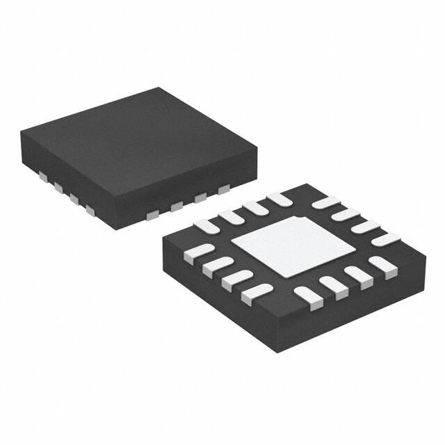
16-Pin WQFN (3.00 mm × 3.00 mm) Package
8-kV ESD Rating on DM/DP Pins
UL Recognized File No. E169910 and CB
Certified - Pending
In addition to charging popular devices, the TPS2547
also supports two distinct power management
features, namely, power wake and port power
management (PPM) through the STATUS pin. Power
wake allows for power supply control in S4/S5
charging and PPM supports intelligent port power
management in multiport systems. Additionally,
system wake up (from S3) with a mouse/keyboard
(both low speed and full speed) is fully supported in
the TPS2547.
The TPS2547 73-mΩ power-distribution switch is
intended for applications where heavy capacitive
loads and short-circuits are likely to be encountered.
Two programmable current thresholds provide
flexibility for setting current limits and load detect
thresholds.
Device Information(1)
PART NUMBER
PACKAGE
BODY SIZE (NOM)
2 Applications
TPS2547
•
•
•
(1) For all available packages, see the orderable addendum at
the end of the data sheet.
USB Ports (Host and Hubs)
Notebook and Desktop PCs
Universal Wall-Charging Adapters
WQFN (16)
3.00 mm × 3.00 mm
Simplified Schematic
To Portable Device à
Power Bus
4.5V – 5.5V
RSTATUS
(10 kW)
STATUS Signal
Fault Signal
ILIM Select
Power Switch EN
Mode Select I/O
0.1 uF
IN
OUT
TPS2547
RFAULT
(10 kW)
CUSB
ILIM_LO
ILIM_HI
STATUS
RILIM_HI
FAULT
ILIM_SEL
EN
CTL1
CTL2
CTL3
VBUS
DD+
GND
RILIM_LO
GND
DM_IN
DP_IN
DM_OUT
DP_OUT
USB
Connector
To Host Controller à
Copyright © 2017, Texas Instruments Incorporated
1
An IMPORTANT NOTICE at the end of this data sheet addresses availability, warranty, changes, use in safety-critical applications,
intellectual property matters and other important disclaimers. PRODUCTION DATA.
�TPS2547
SLVSE11A – MAY 2017 – REVISED MAY 2017
www.ti.com
Table of Contents
1
2
3
4
5
6
Features ..................................................................
Applications ...........................................................
Description .............................................................
Revision History.....................................................
Pin Configuration and Functions .........................
Specifications.........................................................
6.1
6.2
6.3
6.4
6.5
6.6
6.7
6.8
7
8
1
1
1
2
3
4
Absolute Maximum Ratings ...................................... 4
ESD Ratings.............................................................. 4
Recommended Operating Conditions....................... 4
Thermal Information .................................................. 5
Electrical Characteristics........................................... 5
Electrical Characteristics: High-Bandwidth Switch.... 6
Electrical Characteristics: Charging Controller ......... 7
Typical Characteristics .............................................. 9
Parameter Measurement Information ................ 13
Detailed Description ............................................ 14
8.1 Overview ................................................................. 14
8.2 Functional Block Diagram ....................................... 15
8.3 Feature Description................................................. 15
8.4 Device Functional Modes........................................ 26
9
Application and Implementation ........................ 29
9.1 Application Information............................................ 29
9.2 Typical Application .................................................. 30
10 Power Supply Recommendations ..................... 32
11 Layout................................................................... 32
11.1 Layout Guidelines ................................................. 32
11.2 Layout Example .................................................... 33
12 Device and Documentation Support ................. 34
12.1
12.2
12.3
12.4
12.5
12.6
Documentation Support .......................................
Receiving Notification of Documentation Updates
Community Resources..........................................
Trademarks ...........................................................
Electrostatic Discharge Caution ............................
Glossary ................................................................
34
34
34
34
34
34
13 Mechanical, Packaging, and Orderable
Information ........................................................... 34
4 Revision History
NOTE: Page numbers for previous revisions may differ from page numbers in the current version.
Changes from Original (May 2017) to Revision A
Page
•
Changed Equation 1 ............................................................................................................................................................ 30
•
Changed Equation 2 ............................................................................................................................................................ 31
•
Changed Equation 3 ............................................................................................................................................................ 31
2
Submit Documentation Feedback
Copyright © 2017, Texas Instruments Incorporated
Product Folder Links: TPS2547
�TPS2547
www.ti.com
SLVSE11A – MAY 2017 – REVISED MAY 2017
5 Pin Configuration and Functions
GND
FAULT
13
3
10
DP_IN
4
9
7
8
CTL3
ILIM_SEL
14
DM_IN
CTL2
DP_OUT
ILIM_LO
11
Thermal Pad
6
2
15
OUT
CTL1
DM_OUT
ILIM_HI
12
5
1
EN
IN
16
RTE Package
16-Pin WQFN
Top View
STATUS
Not to scale
Pin Functions
PIN
NO.
NAME
TYPE (1)
DESCRIPTION
Input voltage and supply voltage; connect 0.1 μF or greater ceramic capacitor from IN to GND as close
to the device as possible.
1
IN
P
2
DM_OUT
I/O
D– data line to USB host controller.
3
DP_OUT
I/O
D+ data line to USB host controller.
4
ILIM_SEL
I
Logic-level input signal used to control the charging mode, current limit threshold, and load detection;
see Table 3. Can be tied directly to IN or GND without pullup or pulldown resistor.
5
EN
I
Logic-level input for turning the power switch and the signal switches on/off; logic low turns off the signal
and power switches and holds OUT in discharge. Can be tied directly to IN or GND without pullup or
pulldown resistor.
6
CTL1
I
Logic-level input used to control the charging mode and the signal switches; see Table 3. Can be tied
directly to IN or GND without pullup or pulldown resistor.
7
CTL2
I
Logic-level input used to control the charging mode and the signal switches; see Table 3. Can be tied
directly to IN or GND without pullup or pulldown resistor.
8
CTL3
I
Logic-level input used to control the charging mode and the signal switches; see Table 3. Can be tied
directly to IN or GND without pullup or pulldown resistor.
9
STATUS
O
Active-low open-drain output, asserted in load detection conditions.
10
DP_IN
I/O
D+ data line to downstream connector.
11
DM_IN
I/O
D– data line to downstream connector.
12
OUT
P
Power-switch output.
13
FAULT
O
Active-low open-drain output, asserted during overtemperature or current limit conditions.
14
GND
P
Ground connection.
15
ILIM_LO
I
External resistor connection used to set the low current-limit threshold and the load detection current
threshold. A resistor to ILIM_LO is optional; see Current-Limit Settings in Detailed Description.
16
ILIM_HI
I
External resistor connection used to set the high-current-limit threshold.
—
Thermal
Pad
—
(1)
Internally connected to GND; used to heatsink the part to the circuit board traces. Connect to GND
plane.
G = ground, I = input, O = output, P = power.
Submit Documentation Feedback
Copyright © 2017, Texas Instruments Incorporated
Product Folder Links: TPS2547
3
�TPS2547
SLVSE11A – MAY 2017 – REVISED MAY 2017
www.ti.com
6 Specifications
6.1 Absolute Maximum Ratings
Over operating free-air temperature range (unless otherwise noted) (1)
IN, EN, ILIM_LO, ILIM_HI, FAULT, STATUS,
ILIM_SEL, CTL1, CTL2, CTL3, OUT
Voltage
IN to OUT
DP_IN, DM_IN, DP_OUT, DM_OUT
MIN
MAX
UNIT
–0.3
7
–7
7
–0.3
(IN + 0.3) or 5.7
V
Input clamp current
DP_IN, DM_IN, DP_OUT, DM_OUT
±20
mA
Continuous current in SDP or CDP
mode
DP_IN to DP_OUT or DM_IN to DM_OUT
±100
mA
Continuous current in BC1.2 DCP mode
DP_IN to DM_IN
±50
mA
Continuous output current
OUT
Continuous output sink current
FAULT, STATUS
Continuous output source current
ILIM_LO, ILIM_HI
Internally limited
25
Operating junction temperature, TJ
(1)
mA
Internally limited
–40
mA
Internally limited
°C
Stresses beyond those listed under Absolute Maximum Ratings may cause permanent damage to the device. These are stress ratings
only, which do not imply functional operation of the device at these or any other conditions beyond those indicated under Recommended
Operating Conditions. Exposure to absolute-maximum-rated conditions for extended periods may affect device reliability.
6.2 ESD Ratings
VALUE
V(ESD)
Electrostatic
discharge
Human-body model (HBM), per
ANSI/ESDA/JEDEC JS-001 (1)
HBM
±2000
HBM wrt GND and each other, DP_IN,
DM_IN, OUT
±8000
Charged-device model (CDM), per JEDEC specification JESD22-C101 (2)
(1)
(2)
UNIT
V
±500
JEDEC document JEP155 states that 500-V HBM allows safe manufacturing with a standard ESD control process.
JEDEC document JEP157 states that 250-V CDM allows safe manufacturing with a standard ESD control process.
6.3 Recommended Operating Conditions
voltages are referenced to GND (unless otherwise noted)
MIN MAX
VIN
Input voltage, IN
UNIT
4.5
5.5
V
Input voltage, logic-level inputs, EN, CTL1, CTL2, CTL3, ILIM_SEL
0
5.5
V
Input voltage, data line inputs, DP_IN, DM_IN, DP_OUT, DM_OUT
0
VIN
V
VIH
High-level input voltage, EN, CTL1, CTL2, CTL3, ILIM_SEL
VIL
Low-level input voltage, EN, CTL1, CTL2, CTL3, ILIM_SEL
1.8
0.8
V
Continuous current, data line inputs, SDP or CDP mode, DP_IN to DP_OUT, DM_IN to DM_OUT
±30
mA
±15
mA
Continuous current, data line inputs, BC1.2 DCP mode, DP_IN to DM_IN
IOUT
Continuous output current, OUT
V
TJ = –40°C to 125°C
0
2.5
TJ = –40°C to 115°C
0
3.0
Continuous output sink current, FAULT, STATUS
A
0
10
mA
RILIM_XX Current-limit set resistors
15.4
750
kΩ
TJ
–40
125
°C
4
Operating virtual junction temperature
Submit Documentation Feedback
Copyright © 2017, Texas Instruments Incorporated
Product Folder Links: TPS2547
�TPS2547
www.ti.com
SLVSE11A – MAY 2017 – REVISED MAY 2017
6.4 Thermal Information
TPS2547
THERMAL METRIC (1)
RTE (WQFN)
UNIT
16 PINS
RθJA
Junction-to-ambient thermal resistance
53.4
°C/W
RθJC(top)
Junction-to-case (top) thermal resistance
51.4
°C/W
RθJB
Junction-to-board thermal resistance
17.2
°C/W
ψJT
Junction-to-top characterization parameter
3.7
°C/W
ψJB
Junction-to-board characterization parameter
20.7
°C/W
RθJC(bot)
Junction-to-case (bottom) thermal resistance
3.9
°C/W
(1)
For more information about traditional and new thermal metrics, see the Semiconductor and IC Package Thermal Metrics application
report.
6.5 Electrical Characteristics
Unless otherwise noted: –40 ≤ TJ ≤ 125°C, 4.5 V ≤ VIN ≤ 5.5 V, VEN = VIN, VILIM_SEL = VIN, VCTL1 = VCTL2 = VCTL3 = VIN. RFAULT =
RSTATUS = 10 kΩ, RILIM_HI = 20 kΩ, RILIM_LO = 80.6 kΩ. Positive currents are into pins. Typical values are at 25°C. All voltages
are with respect to GND.
PARAMETER
TEST CONDITIONS
MIN
TYP MAX
UNIT
POWER SWITCH
RDS(on)
ON resistance (1)
tr
OUT voltage rise time
tf
OUT voltage fall time
ton
OUT voltage turnon time
toff
OUT voltage turnoff time
IREV
Reverse leakage current
TJ = 25°C, IOUT = 2 A
73
84
–40°C ≤ TJ ≤ 85°C, IOUT = 2 A
73
105
–40°C ≤ TJ ≤ 125°C, IOUT = 2 A
VIN = 5 V, CL = 1 µF, RL = 100 Ω (see Figure 23 and
Figure 24)
73
120
0.7
1
1.6
0.2
0.35
0.5
2.7
4
1.7
3
VIN = 5 V, CL = 1 µF, RL = 100 Ω (see Figure 23 and
Figure 25)
VOUT = 5.5 V, VIN = VEN = 0 V, –40 ≤ TJ ≤ 85°C,
Measure IOUT
mΩ
ms
ms
2
µA
630
Ω
DISCHARGE
RDCHG
OUT discharge resistance
400
500
tDCHG_L
Long OUT discharge hold time
Time VOUT < 0.7 V (see Figure 26)
1.3
2
2.9
s
tDCHG_S
Short OUT discharge hold time
Time VOUT < 0.7 V (see Figure 26)
205
310
450
ms
Input pin rising logic threshold
voltage
1
1.35
1.7
V
Input pin falling logic threshold
voltage
0.85
1.15
1.45
EN, ILIMSEL, CTL1, CTL2, CTL3 INPUTS
Hysteresis (2)
Input current
200
mV
Pin voltage = 0 V or 5.5 V
–0.5
0.5
VILIM_SEL = 0 V, RILIM_LO = 210 kΩ
213
250
287
VILIM_SEL = 0 V, RILIM_LO = 80.6 kΩ
598
650
708
VILIM_SEL = 0 V, RILIM_LO = 22.1 kΩ
2200
2365 2530
VILIM_SEL = VIN, RILIM_HI= 20 kΩ
2425
2610 2800
VILIM_SEL = VIN, RILIM_HI = 16.9 kΩ
2875
3085 3300
VILIM_SEL = VIN, RILIM_HI = 15.4 kΩ, TJ = –40°C to 115°C
3150
3375 3600
µA
ILIMSEL CURRENT LIMIT
IOS
tIOS
(1)
(2)
OUT short-circuit current limit (1)
Response time to OUT shortcircuit (2)
VIN = 5 V, R = 0.1Ω, lead length = 2 inches
(see Figure 27)
1.5
mA
µs
Pulse-testing techniques maintain junction temperature close to ambient temperature; Thermal effects must be taken into account
separately.
These parameters are provided for reference only and do not constitute part of TI's published device specifications for purposes of TI's
product warranty.
Submit Documentation Feedback
Copyright © 2017, Texas Instruments Incorporated
Product Folder Links: TPS2547
5
�TPS2547
SLVSE11A – MAY 2017 – REVISED MAY 2017
www.ti.com
Electrical Characteristics (continued)
Unless otherwise noted: –40 ≤ TJ ≤ 125°C, 4.5 V ≤ VIN ≤ 5.5 V, VEN = VIN, VILIM_SEL = VIN, VCTL1 = VCTL2 = VCTL3 = VIN. RFAULT =
RSTATUS = 10 kΩ, RILIM_HI = 20 kΩ, RILIM_LO = 80.6 kΩ. Positive currents are into pins. Typical values are at 25°C. All voltages
are with respect to GND.
PARAMETER
TEST CONDITIONS
MIN
TYP MAX
UNIT
SUPPLY CURRENT
IIN_OFF
Disabled IN supply current
IIN_ON
Enabled IN supply current
VEN = 0 V, VOUT = 0 V, –40 ≤ TJ ≤ 85°C
0.1
2
VCTL1 = VCTL2 = VIN, VCTL3 = 0 V, VILIM_SEL = 0 V
165
220
VCTL1 = VCTL2 = VCTL3 = VIN, VILIM_SEL = 0 V
175
230
VCTL1 = VCTL2 = VIN, VCTL3 = 0 V, VILIM_SEL = VIN
185
240
VCTL1 = VCTL2 = VIN, VCTL3 = VIN, VILIM_SEL = VIN
195
250
VCTL1 = 0 V, VCTL2 = VCTL3 = VIN
215
270
4.1
4.3
µA
µA
UNDERVOLTAGE LOCKOUT
VUVLO
IN rising UVLO threshold voltage
3.9
Hysteresis (2)
100
V
mV
FAULT
Output low voltage
IFAULT = 1 mA
OFF-state leakage
VFAULT = 5.5 V
Overcurrent FAULT rising and
falling deglitch
5
8.2
100
mV
1
µA
12
ms
100
mV
1
µA
STATUS
Output low voltage
ISTATUS = 1 mA
OFF-state leakage
VSTATUS = 5.5 V
THERMAL SHUTDOWN
Thermal shutdown threshold
155
Thermal shutdown threshold in
current-limit
135
Hysteresis (2)
°C
20
6.6 Electrical Characteristics: High-Bandwidth Switch
Unless otherwise noted: –40 ≤ TJ ≤ 125°C, 4.5 V ≤ VIN ≤ 5.5 V, VEN = VIN, VILIM_SEL = VIN, VCTL1 = VCTL2 = VCTL3 = VIN. RFAULT =
RSTATUS = 10 kΩ, RILIM_HI = 20 kΩ, RILIM_LO = 80.6 kΩ. Positive currents are into pins. Typical values are at 25°C. All voltages
are with respect to GND.
PARAMETER
TEST CONDITIONS
MIN
TYP MAX
UNIT
HIGH-BANDWIDTH ANALOG SWITCH
DP/DM switch ON resistance
VDP/DM_OUT = 0 V, IDP/DM_IN = 30 mA
2
4
VDP/DM_OUT = 2.4 V, IDP/DM_IN = –15 mA
3
6
Switch resistance mismatch between
DP / DM channels
VDP/DM_OUT = 0 V, IDP/DM_IN = 30 mA
0.05
0.15
VDP/DM_OUT = 2.4 V, IDP/DM_IN = –15 mA
0.05
0.15
DP/DM switch OFF-state capacitance (1)
VEN= 0 V, VDP/DM_IN = 0.3 V, Vac = 0.6 Vpk–pk,
f = 1 MHz
3
3.6
6.2
DP/DM switch ON-state capacitance
(2)
Ω
Ω
pF
VDP/DM_IN = 0.3 V, Vac = 0.6 Vpk-pk, f = 1 MHz
5.4
OIRR
OFF-state isolation (3)
VEN= 0 V, f = 250 MHz
33
dB
XTALK
ON-state cross channel isolation (3)
f = 250 MHz
52
dB
OFF-state leakage current
VEN = 0 V, VDP/DM_IN = 3.6 V, VDP/DM_OUT = 0 V,
measure IDP/DM_OUT
0.1
Bandwidth (–3 dB) (3)
RL = 50 Ω
2.6
GHz
0.25
ns
BW
tpd
(1)
(2)
(3)
6
Propagation delay
(3)
1.5
pF
µA
The resistance in series with the parasitic capacitance to GND is typically 250 Ω.
The resistance in series with the parasitic capacitance to GND is typically 150 Ω
These parameters are provided for reference only and do not constitute part of TI's published device specifications for purposes of TI's
product warranty.
Submit Documentation Feedback
Copyright © 2017, Texas Instruments Incorporated
Product Folder Links: TPS2547
�TPS2547
www.ti.com
SLVSE11A – MAY 2017 – REVISED MAY 2017
Electrical Characteristics: High-Bandwidth Switch (continued)
Unless otherwise noted: –40 ≤ TJ ≤ 125°C, 4.5 V ≤ VIN ≤ 5.5 V, VEN = VIN, VILIM_SEL = VIN, VCTL1 = VCTL2 = VCTL3 = VIN. RFAULT =
RSTATUS = 10 kΩ, RILIM_HI = 20 kΩ, RILIM_LO = 80.6 kΩ. Positive currents are into pins. Typical values are at 25°C. All voltages
are with respect to GND.
PARAMETER
TEST CONDITIONS
MIN
TYP MAX
Skew between opposite transitions of the
same port (tPHL – tPLH)
tSK
0.1
UNIT
0.2
ns
6.7 Electrical Characteristics: Charging Controller
Unless otherwise noted: –40 ≤ TJ ≤ 125°C, 4.5 V ≤ VIN ≤ 5.5 V, VEN = VIN, VILIM_SEL = VIN, VCTL1 = 0 V, VCTL2 = VCTL3 = VIN.
RFAULT = RSTATUS = 10 kΩ, RILIM_HI = 20 kΩ, RILIM_LO = 80.6 kΩ. Positive currents are into pins. Typical values are at 25°C. All
voltages are with respect to GND.
PARAMETER
TEST CONDITIONS
MIN
TYP MAX
UNIT
SHORTED MODE (BC1.2 DCP)
DP_IN / DM_IN shorting resistance
VCTL1 = VIN, VCTL2 = VCTL3 = 0 V
125
200
1.19
1.25
1.31
V
60
75
94
kΩ
V
Ω
1.2 V MODE
DP_IN /DM_IN output voltage
DP_IN /DM_IN output impedance
VCTL1 = VIN, VCTL2 = VCTL3 = 0 V
DIVIDER1 MODE
DP_IN divider1 output voltage
1.9
2
2.1
DM_IN divider1 output voltage
2.57
2.7
2.84
V
8
10.5
12.5
kΩ
8
10.5
12.5
kΩ
DP_IN divider2 output voltage
2.57
2.7
2.84
V
DM_IN divider2 output voltage
1.9
2
2.1
V
8
10.5
12.5
kΩ
8
10.5
12.5
kΩ
0.5
0.6
0.7
V
0.4
V
DP_IN output impedance
VCTL1 = VIN, VCTL2 = VCTL3 = 0 V
DM_IN output impedance
DIVIDER2 MODE
DP_IN output impedance
IOUT = 1 A
DM_IN output impedance
CHARGING DOWNSTREAM PORT
VDM_SRC
DM_IN CDP output voltage
VDAT_REF
DP_IN rising lower window threshold
for VDM_SRC activation
Hysteresis (1)
VLGC_SRC
DP_IN rising upper window threshold
for VDM_SRC de-activation
VCTL1 = VCTL2 = VCTL3 =
VIN
VDP_IN = 0.6 V,
–250 µA < IDM_IN < 0 µA
0.25
50
VCTL1 = VCTL2 = VCTL3 = VIN
0.8
Hysteresis (1)
IDP_SINK
DP_IN sink current
mV
1
100
VCTL1 = VCTL2 = VCTL3 =
VIN
VDP_IN = 0.6 V
V
mV
40
70
100
µA
635
700
765
mA
Load detect set time
140
200
275
ms
Load detect reset time
1.9
3
4.2
s
LOAD DETECT – NON-POWER WAKE
IOUT rising load detect current
threshold
ILD
Hysteresis
tLD_SET
(1)
(1)
50
VCTL1 = VCTL2 = VCTL3 = VIN
mA
These parameters are provided for reference only and do not constitute part of Texas Instrument's published device specifications for
purposes of Texas Instrument's product warranty.
Submit Documentation Feedback
Copyright © 2017, Texas Instruments Incorporated
Product Folder Links: TPS2547
7
�TPS2547
SLVSE11A – MAY 2017 – REVISED MAY 2017
www.ti.com
Electrical Characteristics: Charging Controller (continued)
Unless otherwise noted: –40 ≤ TJ ≤ 125°C, 4.5 V ≤ VIN ≤ 5.5 V, VEN = VIN, VILIM_SEL = VIN, VCTL1 = 0 V, VCTL2 = VCTL3 = VIN.
RFAULT = RSTATUS = 10 kΩ, RILIM_HI = 20 kΩ, RILIM_LO = 80.6 kΩ. Positive currents are into pins. Typical values are at 25°C. All
voltages are with respect to GND.
PARAMETER
TEST CONDITIONS
MIN
TYP MAX
UNIT
LOAD DETECT – POWER WAKE
IOS_PW
Power wake short-circuit current limit
IOUT falling power wake reset current
detection threshold
Reset current hysteresis
VCTL1 = VCTL2 = 0 V, VCTL3 = VIN
55
78
mA
23
45
67
mA
(1)
5
Power wake reset time
8
32
10.7
Submit Documentation Feedback
15
mA
20.6
s
Copyright © 2017, Texas Instruments Incorporated
Product Folder Links: TPS2547
�TPS2547
www.ti.com
SLVSE11A – MAY 2017 – REVISED MAY 2017
6.8 Typical Characteristics
0.3
100
0.25
Reverse Leakage Current (µA)
On Resistance (mΩ)
90
80
70
60
0.2
0.15
0.1
0.05
50
−40 −25 −10
5
20 35 50 65 80
Junction Temperature (°C)
95
0
−40 −25 −10
110 125
5
20 35 50 65 80
Junction Temperature (°C)
95
110 125
G001
Figure 1. Power Switch ON Resistance vs Temperature
G002
Figure 2. Reverse Leakage Current vs Temperature
580
3000
OUT Short Circuit Current Limit (mA)
OUT Discharge Resistance (Ω)
560
3500
VIN = 4.5 V
VIN = 5 V
VIN = 5.5 V
540
520
500
480
2500
2000
1500
RILIM_LO = 210 kΩ
RILIM_LO = 80.6 kΩ
RILIM_HI = 20 kΩ
RILIM_HI = 16.9 kΩ
1000
500
460
−40 −25 −10
5
20 35 50 65 80
Junction Temperature (°C)
95
0
−40 −25 −10
110 125
5
20 35 50 65 80
Junction Temperature (°C)
95
110 125
G003
Figure 3. OUT Discharge Resistance vs Temperature
G004
Figure 4. OUT Short-Circuit Current Limit vs Temperature
1.2
190
VIN = 5.5 V
180
Enabled IN Supply Current (µA)
Disabled IN Supply Current (µA)
1
0.8
0.6
0.4
0.2
0
−40
VIN = 4.5 V
VIN = 5 V
VIN = 5.5 V
170
160
150
Device configured for SDP
VILIMSEL = 0 V
140
−20
0
20
40
60
Junction Temperature (°C)
80
100
130
−40 −25 −10
G005
Figure 5. Disabled in Supply Current vs Temperature
5
20 35 50 65 80
Junction Temperature (°C)
95
110 125
G006
Figure 6. Enabled in Supply Current - SDP vs Temperature
Submit Documentation Feedback
Copyright © 2017, Texas Instruments Incorporated
Product Folder Links: TPS2547
9
�TPS2547
SLVSE11A – MAY 2017 – REVISED MAY 2017
www.ti.com
Typical Characteristics (continued)
220
240
VIN = 4.5 V
VIN = 5 V
VIN = 5.5 V
230
Enabled IN Supply Current (µA)
Enabled IN Supply Current (µA)
210
VIN = 4.5 V
VIN = 5 V
VIN = 5.5 V
200
190
180
170
220
210
200
190
Device configured for CDP
160
−40 −25 −10
5
20 35 50 65 80
Junction Temperature (°C)
95
Device configured for DCP AUTO
180
−40 −25 −10
110 125
5
20 35 50 65 80
Junction Temperature (°C)
G007
95
110 125
G008
Figure 7. Enabled in Supply Current - CDP vs Temperature
Figure 8. Enabled in Supply Current - DCP Auto
vs Temperature
0
700
TJ = −40°C
TJ = 25°C
TJ = 125°C
600
Transmission Gain - dB
Output Low Voltage (mV)
-5
500
400
300
200
-10
-15
-20
100
VIN = 4.5 V
0
0
1
2
3
4
5
6
7
Sinking Current (mA)
8
9
-20
10
0.01
Figure 9. Status and Fault Output Low Voltage
vs Sinking Current
10
XTALK - ON State Cross-Channel Isolation - dB
80
50
OIRR - Off State Isolation - dB
1
Figure 10. Data Transmission Characteristics vs Frequency
60
40
30
20
10
70
60
50
40
30
20
10
0
0
0.01
0.1
1
10
0.01
0.1
1
10
Frequency - GHz
Frequency - GHz
Figure 11. OFF-State Data Switch Isolation vs Frequency
10
0.1
Frequency - GHz
G009
Figure 12. ON-State Cross-Channel Isolation vs Frequency
Submit Documentation Feedback
Copyright © 2017, Texas Instruments Incorporated
Product Folder Links: TPS2547
�TPS2547
www.ti.com
SLVSE11A – MAY 2017 – REVISED MAY 2017
0.5
0.5
0.4
0.4
0.3
0.3
0.2
0.2
Differential Signal (V)
Differential Signal (V)
Typical Characteristics (continued)
0.1
0
–0.1
–0.2
0.1
0
–0.1
–0.2
–0.3
–0.3
–0.4
–0.4
–0.5
–0.5
0
0.2
0.4
0.6
0.8
1 1.2
Time (ns)
1.4
1.6
1.8
0
2
0.2
0.4
G013
Figure 13. Eye Diagram Using USB Compliance Test Pattern
(With No Switch)
0.6
0.8
1 1.2
Time (ns)
1.4
1.6
1.8
2
G014
Figure 14. Eye Diagram Using USB Compliance Test Pattern
(With Data Switch)
230
740
RILIM_LO = 80.6 kΩ
720
225
Load Detect Set Time (ms)
Current (mA)
700
680
660
640
220
215
210
205
620
IOS - OUT Short Circuit Current Limit
ILD - IOUT Rising Load Detect Threshold
600
−40 −25 −10
5
20 35 50 65 80
Junction Temperature (°C)
95
110 125
200
−40 −25 −10
5
20 35 50 65 80
Junction Temperature (°C)
95
G015
Figure 15. IOUT Rising Load Detect Threshold and Out
Short-Circuit Current Limit vs Temperature
110 125
G016
Figure 16. Load Detect Set Time vs Temperature
59
Power Wake Current Limit (mA)
58
57
VOUT
2 V/div
56
55
VEN
5 V/div
54
53
52
−40 −25 −10
IIN
500 mA/div
5
20 35 50 65 80
Junction Temperature (°C)
95
RLOAD = 5 Ω
CLOAD = 150 µF
110 125
G017
Figure 17. Power Wake Current Limit vs Temperature
t - Time - 1 ms/div
G021
Figure 18. Turnon Response
Submit Documentation Feedback
Copyright © 2017, Texas Instruments Incorporated
Product Folder Links: TPS2547
11
�TPS2547
SLVSE11A – MAY 2017 – REVISED MAY 2017
www.ti.com
Typical Characteristics (continued)
V/FAULT
5 V/div
VOUT
2 V/div
VEN
5 V/div
VEN
5 V/div
RLOAD = 5 Ω
CLOAD = 150 µF
IIN
500 mA/div
IIN
500 mA/div
t - Time - 1 ms/div
t - Time - 2 ms/div
G022
G023
Figure 20. Device Enabled Into Short-Circuit
Figure 19. Turnoff Response
RILM_HI = 20 kΩ
V/FAULT
5 V/div
RILM_LO = 80.6 kΩ
V/FAULT
5 V/div
VEN
5 V/div
VOUT
2 V/div
IIN
1 A/div
IIN
2 A/div
t - Time - 5 ms/div
t - Time - 2 ms/div
G024
Figure 21. Device Enabled Into Short-Circuit - Thermal
Cycling
12
RILIM_HI = 20 kΩ
RLOAD = 5 Ω
CLOAD = 150 µF
G025
Figure 22. Short-Circuit to Full Load Recovery
Submit Documentation Feedback
Copyright © 2017, Texas Instruments Incorporated
Product Folder Links: TPS2547
�TPS2547
www.ti.com
SLVSE11A – MAY 2017 – REVISED MAY 2017
7 Parameter Measurement Information
OUT
RL
CL
Figure 23. Out Rise/Fall Test Load
VOUT
tr
90%
tf
10%
Figure 24. Power-ON and OFF Timing
50 %
VEN
50 %
ton
toff
90 %
VOUT
10 %
Figure 25. Enable Timing, Active High Enable
5V
tDCHG
VOUT
0V
Figure 26. Out Discharge During Mode Change
IOS
IOUT
tIOS
Figure 27. Output Short-Circuit Parameters
Submit Documentation Feedback
Copyright © 2017, Texas Instruments Incorporated
Product Folder Links: TPS2547
13
�TPS2547
SLVSE11A – MAY 2017 – REVISED MAY 2017
www.ti.com
8 Detailed Description
8.1 Overview
The following overview references various industry standards. TI recommends consulting the most up-to-date
standard to ensure the most recent and accurate information. Rechargeable portable equipment requires an
external power source to charge its batteries. USB ports are a convenient location for charging, because of an
available 5-V power source. Universally accepted standards are required to make sure host and client-side
devices operate together in a system to ensure power management requirements are met. Traditionally, host
ports following the USB 2.0 specification must provide at least 500 mA to downstream client-side devices.
Because multiple USB devices can attach to a single USB port through a bus-powered hub, it is the responsibility
of the client-side device to negotiate its power allotment from the host, ensuring the total current draw does not
exceed 500 mA. In general, each USB device is granted 100 mA, and may request more current in 100-mA unit
steps up to 500 mA. The host may grant or deny based on the available current. A USB 3.0 host port not only
provides higher data rate than USB 2.0 port, but also raises the unit load from 100 mA to 150 mA. It is also
required to provide a minimum current of 900 mA to downstream client-side devices.
Additionally, the success of USB makes the mini-USB connector a popular choice for wall adapter cables. This
allows a portable device to charge from both a wall adapter, and USB port with only one connector. As USB
charging has gained popularity, the 500-mA minimum defined by USB 2.0 or 900 mA for USB 3.0 has become
insufficient for many handset and personal media players, which need a higher charging rate. Wall adapters can
provide much more current than 500 mA/900 mA. Several new standards have been introduced, defining
protocol handshaking methods that allow host and client devices to acknowledge and draw additional current
beyond the 500 mA/900 mA minimum defined by USB 2.0 and 3.0, while still using a single micro-USB input
connector.
The TPS2547 supports four of the most common USB charging schemes found in popular handheld media and
cellular devices:
• USB Battery Charging Specification BC1.2
• Chinese Telecommunications Industry Standard YD/T 1591-2009
• Divider Mode
• 1.2-V Mode
YD/T 1591-2009 is a subset of BC1.2 specifications supported by vast majority of devices that implement USB
changing. Divider and 1.2-V charging schemes are supported in devices from specific, yet popular device
makers.
BC1.2 lists three different port types:
• Standard Downstream Port (SDP)
• Charging Downstream Port (CDP)
• Dedicated Charging Port (DCP)
BC1.2 defines a charging port as a downstream facing USB port that provides power for charging portable
equipment. Under this definition, CDP and DCP are defined as charging ports.
14
Submit Documentation Feedback
Copyright © 2017, Texas Instruments Incorporated
Product Folder Links: TPS2547
�TPS2547
www.ti.com
SLVSE11A – MAY 2017 – REVISED MAY 2017
8.2 Functional Block Diagram
Current
Sense
CS
IN
OUT
Disable + UVLO+Discharge
ILIM_HI
Current
Limit
Current Limit
select
Charge
Pump
ILIM_LO
GND
OC
8-ms Deglitch
OTSD
Thermal
Sense
UVLO
ILIM_SEL
Driver
LD cur set
EN
discharge
FAULT
8-ms Deglitch
(falling edge)
DM_OUT
DM_IN
DP_OUT
DP_IN
ILIM_SEL
OC
CTL1
CTL2
Logic
control
CDP
Detection
DCP
Detection
Divider
Mode
Auto-Detection
LD cur set
Discharge
STATUS
TPS2543
Only
CTL3
Discharge
Copyright © 2016, Texas Instruments Incorporated
8.3 Feature Description
8.3.1 Standard Downstream Port (SDP) USB 2.0/USB 3.0
An SDP is a traditional USB port that follows USB 2.0 and 3.0 protocol, and supplies a minimum of 500 mA for
USB 2.0 and 900 mA for USB 3.0 per port. USB 2.0 and 3.0 communications is supported, and the host
controller must be active to allow charging. TPS2547 supports SDP mode in system power state S0, when
system is completely powered ON, and fully operational. For more details on control pin (CTL1-CTL3) settings to
program this state, see Table 3.
Submit Documentation Feedback
Copyright © 2017, Texas Instruments Incorporated
Product Folder Links: TPS2547
15
�TPS2547
SLVSE11A – MAY 2017 – REVISED MAY 2017
www.ti.com
Feature Description (continued)
8.3.2 Charging Downstream Port (CDP)
A CDP is a USB port that follows USB BC1.2 and supplies a minimum of 1.5 A per port. It provides power and
meets USB 2.0 requirements for device enumeration. USB 2.0 communications is supported, and the host
controller must be active to allow charging. What separates a CDP from an SDP is the host-charge handshaking
logic that identifies this port as a CDP. A CDP is identifiable by a compliant BC1.2 client device, and allows for
additional current draw by the client device.
The CDP process is done in two steps. During step one, the portable equipment outputs a nominal 0.6-V output
on the D+ line, and reads the voltage input on the D– line. The portable device detects it is connected to an SDP
if the D– voltage is less than the nominal data detect voltage of 0.3 V. The portable device detects that it is
connected to a Charging Port if the D– voltage is greater than the nominal data detect voltage of 0.3 V, and
optionally less than 0.8 V.
The second step is necessary for portable equipment to determine if it is connected to CDP or DCP. The
portable device outputs a nominal 0.6 V output on its D– line, and reads the voltage input on its D+ line. The
portable device detects it is connected to a CDP if the data line being read remains less than the nominal data
detect voltage of 0.3 V. The portable device detects it is connected to a DCP if the data line being read is greater
than the nominal data detect voltage of 0.3 V.
TPS2547 supports CDP mode in system power state S0 when system is completely powered ON, and fully
operational. For more details on control pin (CTL1-CTL3) settings to program this state, see Table 3.
8.3.3 Dedicated Charging Port (DCP)
A DCP only provides power but does not support data connection to an upstream port. As shown in following
sections, a DCP is identified by the electrical characteristics of the data lines. The TPS2547 emulates DCP in
two charging states, namely DCP Forced and DCP Auto as shown in Figure 37. In DCP Forced state the device
supports one of the two DCP charging schemes, namely Divider1 or Shorted. In the DCP Auto state, the device
charge detection state machine is activated to selectively implement charging schemes involved with the
Shorted, Divider1, Divider2, and 1.2-V modes. Shorted DCP mode complies with BC1.2 and Chinese
Telecommunications Industry Standard YD/T 1591-2009, while the Divider and 1.2-V modes are employed to
charge devices that do not comply with BC1.2 DCP standard.
8.3.3.1 DCP BC1.2 and YD/T 1591-2009
Both standards define that the D+ and D– data lines must be shorted together with a maximum series impedance
of 200 Ω. This is shown in Figure 28.
TPS2547
D- Out
VBUS
USB Host/Hub
2.0 V
Auto
Detect
Connector
2.7 V
CDP
Detect
USB
1.2 V
< 200 Ÿ
D-
D+
GND
D+ Out
Copyright © 2017, Texas Instruments Incorporated
Figure 28. DCP Supporting BC1.2/YD/T 1591-2009
16
Submit Documentation Feedback
Copyright © 2017, Texas Instruments Incorporated
Product Folder Links: TPS2547
�TPS2547
www.ti.com
SLVSE11A – MAY 2017 – REVISED MAY 2017
Feature Description (continued)
8.3.3.2 DCP Divider Charging Scheme
There are two Divider charging scheme supported by the device, Divider1 and Divider2 as shown in Figure 29
and Figure 30. In Divider1 charging scheme the device applies 2 V and 2.7 V to D+ and D– data line
respectively. This is reversed in Divider2 mode.
TPS2547
D- Out
VBUS
2.7 V
Auto
Detect
Connector
2.0 V
CDP
Detect
USB
1.2 V
< 200 Ÿ
USB Host/Hub
D-
D+
GND
D+ Out
Copyright © 2017, Texas Instruments Incorporated
Figure 29. DCP Divider1 Charging Scheme
D- Out
TPS2547
VBUS
USB Host/Hub
2.0 V
Auto
Detect
Connector
2.7 V
CDP
Detect
USB
1.2 V
< 200 Ÿ
D-
D+
GND
D+ Out
Copyright © 2017, Texas Instruments Incorporated
Figure 30. Divider2 Charging Scheme
Submit Documentation Feedback
Copyright © 2017, Texas Instruments Incorporated
Product Folder Links: TPS2547
17
�TPS2547
SLVSE11A – MAY 2017 – REVISED MAY 2017
www.ti.com
Feature Description (continued)
8.3.3.3 DCP 1.2-V Charging Scheme
1.2-V charging scheme is used by some handheld devices to enable fast charging at 2 A. TPS2547 supports this
scheme in the DCP-Auto mode before the device enters BC1.2 shorted mode. To simulate this charging scheme
D+/D– lines are shorted and pulled-up to 1.2 V for fixed duration then device moves to DCP shorted mode as
defined in BC1.2 specification. This is shown in Figure 31.
D- Out
TPS2547
VBUS
USB Host/Hub
2.0 V
2.7 V
CDP
Detect
Auto
Detect
Connector
1.2 V
USB
< 200 Ÿ
D-
D+
GND
D+ Out
Copyright © 2017, Texas Instruments Incorporated
Figure 31. DCP 1.2-V Charging Scheme
8.3.4 Wake on USB Feature (Mouse/Keyboard Wake Feature)
8.3.4.1 USB 2.0 Background Information
The TPS2547 data lines interface with USB 2.0 devices. USB 2.0 defines three types of devices according to
data rate. These devices and their characteristics relevant to TPS2547 Wake on USB operation are shown
below.
Low-speed USB devices:
• 1.5 Mbps
• Wired mice and keyboards are examples
• No devices that need battery charging
• All signaling performed at 2 V and 0.8 V hi/lo logic levels
• D– high to signal connect and when placed into suspend
• D– high when not transmitting data packets
Full-speed USB devices:
• 12 Mbps
• Wireless mice and keyboards are examples
• Legacy phones and music players are examples
• Some legacy devices that need battery charging
• All signaling performed at 2 V and 0.8 V hi/lo logic levels
• D+ high to signal connect and when placed into suspend
• D+ high when not transmitting data packets
High-speed USB devices:
• 480 Mbps
• Tablets, phones and music players are examples
• Many devices that need battery charging
• Connect and suspend signaling performed at 2 V and 0.8 V hi/lo logic levels
• Data packet signaling performed a logic levels below 0.8 V
• D+ high to signal connect and when placed into suspend (same as a full-speed device)
18
Submit Documentation Feedback
Copyright © 2017, Texas Instruments Incorporated
Product Folder Links: TPS2547
�TPS2547
www.ti.com
SLVSE11A – MAY 2017 – REVISED MAY 2017
Feature Description (continued)
•
D+ and D– low when not transmitting data packets
8.3.4.2 Wake On USB
Wake on USB is the ability of a wake configured USB device to wake a computer system from its S3 sleep state
back to its S0 working state. Wake on USB requires the data lines to be connected to the system USB host
before the system is placed into its S3 sleep state, and remain continuously connected until they are used to
wake the system.
The TPS2547 supports low-speed and high-speed HID (human interface device like mouse/key board) wake
function. There are two scenarios under which wake on mouse are supported by the TPS2547. The specific CTL
pin changes that the TPS2547 overrides are shown below. The information is presented as CTL1, CTL2, CTL3.
The ILIM_SEL pin plays no role.
1. 111 (CDP/SDP2) to 011 (DCP-Auto)
2. 010 (SDP1) to 011 (DCP-Auto)
NOTE
The 110 (SDP1) to 011 (DCP-Auto) transition is not supported. This is done for practical
reasons, because the transition involves changes to two CTL pins. Depending on which
CTL pin changes first, the device sees either a temporary 111 or 010 command. The 010
command is safe but the 111 command causes an OUT discharge as the TPS2547
instead proceeds to the 111 state.
8.3.4.3 USB Slow-Speed and Full-Speed Device Recognition
TPS2547 is capable of detecting LS or FS device attachment when TPS2547 is in SDP or CDP mode. Per USB
specification, when no device is attached, the D+ and D– lines are near ground level. When a low-speed
compliant device is attached to the TPS2547 charging port, D– line is pulled high in its idle state
(mouse/keyboard not activated). However, when a FS device is attached then the opposite is true in its idle state,
that is, D+ is pulled high and D– remains at ground level.
TPS2547 monitors both D+ and D– lines while CTL pin settings are in CDP or SDP mode to detect LS or FS HID
device attachment. To support HID sleep wake, TPS2547 must first determine that it is attached to a LS or FS
device when system is in S0 power state. TPS2547 does this as described above. While supporting a LS HID
wake is straight forward, supporting FS HID requires making a distinction between a FS and a HS device. This is
because a high-speed device always presents itself initially as a full speed device (by a 1.5-K pullup resistor on
D+). The negotiation for high speed then makes the distinction whereby the 1.5-K pullup resistor gets removed.
TPS2547 handles the distinction between a FS and HS device at connect by memorizing if the D+ line goes low
after connect. A HS device after connect always undergoes negotiation for HS, which requires the 1.5-kΩ resistor
pullup on D+ to be removed. To memorize a FS device, TPS2547 requires the device to remain connected for at
least 60 seconds while the system is in S0 mode, before placing it in sleep or S3 mode.
NOTE
If system is placed in sleep mode earlier than the 60 second window, a FS device may not
get recognized and hence could fail to wake system from S3. This requirement does not
apply for LS device.
8.3.4.3.1 No CTL Pin Timing Requirement After Wake Event and Transition from S3 to S0
Unlike the TPS2543, there is no CTL pin timing requirement for the TPS2547 when the wake configured USB
device wakes the system from S3 back to S0. The TPS2543 requires the CTL pins to transition from the DCPAuto setting back to the SDP/CDP setting within 64 ms of the attached USB device signaling a wake event (for
example, mouse clicked or keyboard key pressed). No such timing condition exists for the TPS2547.
Submit Documentation Feedback
Copyright © 2017, Texas Instruments Incorporated
Product Folder Links: TPS2547
19
�TPS2547
SLVSE11A – MAY 2017 – REVISED MAY 2017
www.ti.com
Feature Description (continued)
8.3.5 Load Detect
TPS2547 offers system designers unique power management strategy not available in the industry from similar
devices. There are two power management schemes supported by the TPS2547 through the STATUS pin, they
are:
• Power Wake (PW)
• Port Power Management (PPM)
Either feature may be implemented in a system depending on power savings goals for the system. In general,
Power Wake feature is used mainly in mobile systems, like a notebook, where it is imperative to save battery
power when system is in deep sleep (S4/S5) state. Oppositely, Port Power Management feature would be
implemented where multiple charging ports are supported in the same system, and system power rating is not
capable of supporting high-current charging on multiple ports simultaneously.
8.3.6 Power Wake
The goal of the power wake feature is to save system power when the system is in S4/S5 state. In the S4/S5
state, the system is in deep sleep and typically running off the battery; so every mW in system power savings
translates to extending battery life. In this state, the TPS2547 monitors charging current at the OUT pin and
provide a mechanism through the STATUS pin to switch out the high-power DC-DC controller and switch in a low
power LDO when charging current requirement is < 45 mA (typical). This would be the case when no peripheral
device is connected at the charging port or if a device has attained its full battery charge and draws 55 mA
Power Wake De-asserted
/STATUS = 1
Current Limit = 55 mA
Charging Load Not Detected.
x
TPS2547 is not asserting power wake. System power is in
a low power state to save energy.
x
TPS2547 monitors port to detect when charging load is
attached and tries to charge
Copyright © 2017, Texas Instruments Incorporated
Figure 32. Power Wake Flow Chart
Submit Documentation Feedback
Copyright © 2017, Texas Instruments Incorporated
Product Folder Links: TPS2547
21
�TPS2547
SLVSE11A – MAY 2017 – REVISED MAY 2017
www.ti.com
Feature Description (continued)
8.3.6.1 Implementing Power Wake in Notebook System
An implementation of power wake in notebook platforms with the TPS2547 is shown in Figure 33 to Figure 35.
Power wake function is used to select between a high-power DC-DC converter, and low-power LDO (100 mA)
based on charging requirements. System power saving is achieved when under no charging conditions (the
connected device is fully charged or no device is connected) the DC-DC converter is turned off (to save power
because it is less efficient in low-power operating region) and the low-power LDO supplies standby power to the
charging port.
Power wake is activated in S4/S5 mode (0011 setting, see Table 3), TPS2547 is charging connected device as
shown in Figure 33, STATUS is pulled LO (Case 1) which switches-out the LDO and switches-in the DC-DC
converter to handle high-current charging.
LDO Disconnected/Shut-Down
DC-DC Switched-In
POWER Block
19
V
5 V_DC/DC
EN
5V_LDO
EN
Embedded
Controller
LO
DM_OUT
DP_OUT
FAULT
EN
CTL1
CTL2
CTL3
I/O_Sx
4
USB Host
Controller
VBUS
DD+
GND
Peripheral
Device
CHARGING
USB
Receptacle
ILIM_HI
DM
DP
OC
I/O_EN
Connected
OUT
DM_IN
DP_IN
GND
STATUS
ILIM_LO
Switches Power
between LDO and
DC/DC based on
/STATUS
ilimit set by
Rlim_Hi
TPS2547
IN
ILIM_SEL
0011
Copyright © 2017, Texas Instruments Incorporated
Figure 33. Case 1: System in S4/S5, Device Charging
As shown in Figure 34 and Figure 35, when connected device is fully charged or gets disconnected from the
charging port, the charging current falls. If charging current falls to < 45 mA and stays below this threshold for
over 15 s, TPS2547 automatically sets a 55-mA internal current limit and STATUS is de-asserted (pulled HI). As
shown in Figure 34 and Figure 35. This results in DC-DC converter turning off, and the LDO turning on. Current
limit of 55 mA is set to prevent the low-power LDO output voltage from collapsing in case there is a spike in
current draw due to device attachment or other activity such as display panel LED turning ON in connected
device.
Following Power Wake flow chart (Figure 32) when a device is attached and draws > 55 mA of charging current
the TPS2547 hits its internal current limit. This triggers the device to assert STATUS (LO), and turn on the DCDC converter and turn off the LDO. TPS2547 discharges OUT for > 2 s (typical), allowing the main power supply
to turn on. After the discharge, the device turns back on with current limit set by ILIM_HI (Case 1).
22
Submit Documentation Feedback
Copyright © 2017, Texas Instruments Incorporated
Product Folder Links: TPS2547
�TPS2547
www.ti.com
SLVSE11A – MAY 2017 – REVISED MAY 2017
Feature Description (continued)
DC-DC Disconnected/Shut-Down
LDO Switched-In
Charging current falls to


 工商网监
湘ICP备2023018690号
工商网监
湘ICP备2023018690号
