TPS3619-33,, TPS3619-50
TPS3620-33, TPS3620-50
www.ti.com
SLVS387H – APRIL 2001 – REVISED DECEMBER 2007
BACKUP-BATTERY SUPERVISORS FOR RAM RETENTION
FEATURES
1
DESCRIPTION
• Supply Current of 40 µA (Max)
• Battery-Supply Current of 100 nA (Max)
• Precision Supply Voltage Monitor 3.3 V, 5 V,
Other Options on Request
• Backup-Battery Voltage Can Exceed VDD
• Power On Reset Generator With Fixed 100-ms
Reset Delay Time
• Voltage Monitor For Power-Fail or Low-Battery
Monitoring
• Battery Freshness Seal (TPS3619)
• Pin-For-Pin Compatible With MAX819,
MAX703, and MAX704
• 8-Pin MSOP Package
• Temperature Range –40°C to +85°C
2
The TPS3619 and TPS3620 families of supervisory
circuits monitor and control processor activity by
providing backup-battery switchover for data retention
of CMOS RAM.
During power on, RESET is asserted when the
supply voltage (VDD or VBAT) becomes higher than 1.1
V. Thereafter, the supply voltage supervisor monitors
VDD and keeps RESET output active as long as VDD
remains below the threshold voltage (VIT). An internal
timer delays the return of the output to the inactive
state (high) to ensure proper system reset. The delay
time starts after VDD has risen above VIT. When the
supply voltage drops below VIT, the output becomes
active (low) again.
The product spectrum is designed for supply voltages
of 3.3 V and 5 V. The TPS3619 and TPS3620 are
available in an 8-pin MSOP package and are
characterized for operation over a temperature range
of –40°C to +85°C.
APPLICATIONS
•
•
•
•
•
•
•
•
•
Fax Machines
Set-Top Boxes
Advanced Voice Mail Systems
Portable Battery-Powered Equipment
Computer Equipment
Advanced Modems
Automotive Systems
Portable Long-Time Monitoring Equipment
Point-of-Sale Equipment
DGK PACKAGE
(TOP VIEW)
VOUT
VDD
GND
PFI
1
8
2
7
3
6
4
5
VBAT
RESET
MR
PFO
ACTUAL SIZE
3,05 mm x 4,98 mm
TYPICAL OPERATING CIRCUIT
Power
Supply
TPS3619
TPS3620
0.1 µF
VBAT
VDD
External
Source
Microcontroller
or
Microprocessor
Backup
Battery
RESET
RESET
Rx
PFI
Ry
Manual
Reset
I/O
PFO
Switchover
Capacitor
MR
VOUT
GND
0.1 µF
VCC
GND
1
2
Please be aware that an important notice concerning availability, standard warranty, and use in critical applications of
Texas Instruments semiconductor products and disclaimers thereto appears at the end of this data sheet.
All trademarks are the property of their respective owners.
PRODUCTION DATA information is current as of publication date.
Products conform to specifications per the terms of the Texas
Instruments standard warranty. Production processing does not
necessarily include testing of all parameters.
Copyright © 2001–2007, Texas Instruments Incorporated
�TPS3619-33,, TPS3619-50
TPS3620-33, TPS3620-50
www.ti.com
SLVS387H – APRIL 2001 – REVISED DECEMBER 2007
This integrated circuit can be damaged by ESD. Texas Instruments recommends that all integrated circuits be handled with
appropriate precautions. Failure to observe proper handling and installation procedures can cause damage.
ESD damage can range from subtle performance degradation to complete device failure. Precision integrated circuits may be more
susceptible to damage because very small parametric changes could cause the device not to meet its published specifications.
PACKAGE INFORMATION (1)
SPECIFIED
TEMPERATURE RANGE
PRODUCT
PACKAGE
MARKING
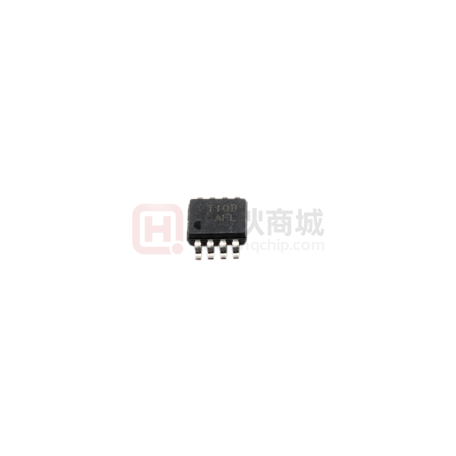
TPS3619-33
AFL
TPS3619-50
AFM
–40°C to +85°C
TPS3620-33
ANL
TPS3620-50
(1)
ANM
ORDERING NUMBER
TRANSPORT MEDIA,
QUANTITY
TPS3619-33DGK
Tube, 80
TPS3619-33DGKR
Tape and Reel, 2500
TPS3619-50DGK
Tube, 80
TPS3619-50DGKR
Tape and Reel, 2500
TPS3620-33DGKT
Tape and Reel, 250
TPS3620-33DGKR
Tape and Reel, 2500
TPS3620-50DGKT
Tape and Reel, 250
TPS3620-50DGKR
Tape and Reel, 2500
For the most current specifications and package information, see the Package Option Addendum located at the end of this data sheet or
refer to our web site at www.ti.com.
STANDARD AND APPLICATION SPECIFIC VERSIONS
TPS361
9 – 33
DGK
R
Reel
Package
Nominal Supply Voltage
Functionality
(1)
Family
DEVICE NAME
NOMINAL VOLTAGE (1), VNOM
TPS3619-33 DGK
3.3 V
TPS3619-50 DGK
5.0 V
TPS3620-33 DGK
3.3 V
TPS3620-50 DGK
5.0 V
For other threshold voltage versions, contact the local TI sales
office for availability and lead-time.
ABSOLUTE MAXIMUM RATINGS
Over operating free-air temperature (unless otherwise noted). (1)
UNIT
Supply voltage:
VDD
(2)
7V
MR and PFI pins (2)
Continuous output current:
–0.3 V to (VDD + 0.3 V)
VOUT, IO
400 mA
All other pins, IO (2)
±10 mA
Continuous total power dissipation
See Dissipation Rating Table
Operating free-air temperature range, TA
–40°C to +85°C
Storage temperature range, Tstg
–65°C to +150°C
Lead temperature soldering 1,6 mm (1/16 inch) from case for 10 seconds
(1)
(2)
+260°C
Stresses beyond those listed under absolute maximum ratings may cause permanent damage to the device. These are stress ratings
only, and functional operation of the device at these or any other conditions beyond those indicated under recommended operating
conditions is not implied. Exposure to absolute-maximum-rated conditions for extended periods may affect device reliability.
All voltage values are with respect to GND. For reliable operation, the device must not be operated at 7 V for more than t = 1000h
continuously.
DISSIPATION RATING TABLE
2
PACKAGE
θJC
θJA
(LOW-K)
θJA
(HIGH-K)
TA < 25°C
POWER RATING
DERATING
FACTOR ABOVE
TA = +25°C
TA= +70°C
POWER RATING
TA = +85°C
POWER RATING
DGK
55°C/W
266°C/W
180°C/W
470 mW
3.76 mW/°C
301 mW
241 mW
Submit Documentation Feedback
Copyright © 2001–2007, Texas Instruments Incorporated
Product Folder Link(s): TPS3619-33 TPS3619-50 TPS3620-33 TPS3620-50
�TPS3619-33,, TPS3619-50
TPS3620-33, TPS3620-50
www.ti.com
SLVS387H – APRIL 2001 – REVISED DECEMBER 2007
RECOMMENDED OPERATING CONDITIONS
At specified temperature range.
MIN
Supply voltage, VDD
Battery supply voltage, VBAT
Input voltage, VI
High-level input voltage, VIH
MAX
UNIT
1.65
5.5
V
1.5
5.5
V
0
VDD + 0.3
V
0.7 x VDD
V
Low-level input voltage, VIL
0.3 x VDD
V
Continuous output current at VOUT, IO
300
mA
Input transition rise and fall rate at MR
100
ns/V
1
V/µs
Slew rate at VDD or VBAT, Δ t/ΔV
Operating free-air temperature range, TA
–40
+85
°C
ELECTRICAL CHARACTERISTICS
Over recommended operating conditions (unless otherwise noted).
PARAMETER
TEST CONDITIONS
RESET
VOH
High-level output voltage
PFO
VOL
Low-level output voltage
Vres
RESET PFO
Power-up reset voltage (see
(1)
)
Normal mode
VOUT
Battery-backup mode
rDS(on)
VIT–
VDD – 0.2 V
IOH = –2 mA
VDD – 0.4 V
VDD = 5 V,
IOH = –3 mA
VDD – 0.4 V
VDD = 1.8 V,
IOH = –20 µA
VDD – 0.3 V
VDD = 3.3 V,
IOH = –80 µA
VDD – 0.4 V
VDD = 5 V,
IOH = –120 µA
VDD – 0.4 V
VDD = 1.8 V,
IOL = –400 µA
0.2
VDD = 3.3 V,
IOL = 2 mA
0.4
VDD = 5 V,
IOL = 3 mA
0.4
VDD = 1.8 V
VDD – 50 mV
IOUT = 125 mA,
VBAT = 0 V
VDD = 3.3 V
VDD – 150 mV
IOUT = 200 mA,
VBAT = 0 V
VDD = 5 V
VDD – 200 mV
IOUT = 0.5 mA,
VBAT = 1.5 V
VDD = 0 V
VBAT – 20 mV
VDD = 3.3 V
TPS3619-33
)
TPS3619-50
TA = –40°C to 85°C
PFI
Hysteresis
(1)
(2)
(3)
V
V
V
V
VBAT – 113 mV
0.6
1
8
15
2.88
2.93
3
4.46
4.55
4.64
1.13
1.15
1.17
1.65 V < VIT < 2.5 V
20
2.5 V < VIT < 3.5 V
40
3.5 V < VIT < 5.5 V
60
PFI
VBSW
(see (3))
V
0.4
IOUT = 8.5 mA,
VBAT = 0 V
UNIT
V
IOL = 20 µA, VBAT > 1.1 V or
VDD > 1.1 V
VDD = 5 V
VIT
Vhys
IOH = –400 µA
IOUT = 7.5 mA,
VBAT = 3.3 V
(2)
MAX
VDD = 3.3 V,
VBAT to VOUT on-resistance
VPFI
TYP
VDD = 1.8 V,
VDD to VOUT on-resistance
Negative-going input
threshold voltage (see
MIN
Ω
V
mV
12
VDD = 1.8 V
55
The lowest supply voltage at which RESET becomes active. tr,VDD ≥ 15 µs/V.
To ensure the best stability of the threshold voltage, a bypass capacitor (ceramic, 0.1 µF) should be placed near the supply terminals.
For VDD < 1.6 V, VOUT switches to VBAT regardless of VBAT.
Copyright © 2001–2007, Texas Instruments Incorporated
Submit Documentation Feedback
Product Folder Link(s): TPS3619-33 TPS3619-50 TPS3620-33 TPS3620-50
3
�TPS3619-33,, TPS3619-50
TPS3620-33, TPS3620-50
www.ti.com
SLVS387H – APRIL 2001 – REVISED DECEMBER 2007
ELECTRICAL CHARACTERISTICS (continued)
Over recommended operating conditions (unless otherwise noted).
PARAMETER
TEST CONDITIONS
IIH
High-level input current
IIL
Low-level input current
II
Input current
PFI
IOS
Short-circuit current
PFO
IDD
VDD supply current
I(BAT)
VBAT supply current
Ci
Input capacitance
MR
MR = 0.7 x VDD
MR = 0 V
PFO = 0 V
MIN
VDD = 5 V
TYP
MAX
–33
–76
–110
–255
–25
25
VDD = 1.8 V
–0.3
VDD = 3.3 V
–1.1
VDD = 5 V
–2.4
VOUT = VDD
40
VOUT = VBAT
40
VOUT = VDD
–0.1
0.1
VOUT = VBAT
0.5
VI = 0 V to 5 V
5
UNIT
µA
nA
mA
µA
µA
pF
TIMING REQUIREMENTS
At RL = 1 MΩ, CL = 50 pF, TA = –40°C to +85°C.
PARAMETER
tw
Pulse width
TEST CONDITIONS
at VDD
VIH = VIT + 0.2 V, VIL = VIT – 0.2 V
at MR
VDD = VIT + 0.2 V, VIL = 0.3 x VDD, VIH = 0.7 x VDD
MIN
TYP
MAX
UNIT
6
µs
100
ns
SWITCHING CHARACTERISTICS
At RL = 1 MΩ, CL= 50 pF, TA= –40°C to +85°C.
PARAMETER
MIN
VDD ≥ VIT+ 0.2 V, MR ≥ 0.7 x VDD
See timing diagram
td
Delay time
tPHL
Propagation (delay) time,
high-to-low level output
4
TEST CONDITIONS
60
TYP
MAX
100
140
VDD to RESET
VIL = VIT – 0.2 V, VIH = VIT + 0.2 V
2
5
PFI to PFO delay
VIL = VPFI – 0.2 V, VIH = VPFI + 0.2 V
3
5
MR to RESET
VDD ≥ VIT+ 0.2 V, VIL= 0.3 x VDD,
VIH = 0.7 x VDD
0.1
1
Submit Documentation Feedback
UNIT
ms
µs
Copyright © 2001–2007, Texas Instruments Incorporated
Product Folder Link(s): TPS3619-33 TPS3619-50 TPS3620-33 TPS3620-50
�TPS3619-33,, TPS3619-50
TPS3620-33, TPS3620-50
www.ti.com
SLVS387H – APRIL 2001 – REVISED DECEMBER 2007
TIMING DIAGRAM
VBAT
VDD
VIT
t
VOUT
t
RESET
td
td
t
Table 1. FUNCTION TABLE
VDD > VIT
VDD > VBAT
MR
VOUT
RESET
0
0
0
VBAT
0
0
0
1
VBAT
0
0
1
0
VDD
0
0
1
1
VDD
0
1
0
0
VDD
0
1
0
1
VDD
1
1
1
0
VDD
0
1
1
1
VDD
1
PFI > VPFI
PFO
0
0
1
1
CONDITION.: VDD > VDD_MIN
Copyright © 2001–2007, Texas Instruments Incorporated
Submit Documentation Feedback
Product Folder Link(s): TPS3619-33 TPS3619-50 TPS3620-33 TPS3620-50
5
�TPS3619-33,, TPS3619-50
TPS3620-33, TPS3620-50
www.ti.com
SLVS387H – APRIL 2001 – REVISED DECEMBER 2007
Table 2. TERMINAL FUNCTIONS
TERMINAL
NAME
I/O
NO.
DESCRIPTION
GND
3
I
Ground
MR
6
I
Manual reset input
PFI
4
I
Power-fail comparator input
PFO
5
O
Power-fail comparator output
RESET
7
O
Active-low reset output
VBAT
8
I
Backup-battery input
VDD
2
I
Input supply voltage
VOUT
1
O
Supply output
FUNCTIONAL BLOCK DIAGRAM
TPS3619
TPS3620
VBAT
+
_
Switch
Control
VOUT
VDD
MR
+
_
PFI
RESET
Logic
+
Timer
RESET
_
+
PFO
Reference
Voltage
of 1.15 V
6
Submit Documentation Feedback
Copyright © 2001–2007, Texas Instruments Incorporated
Product Folder Link(s): TPS3619-33 TPS3619-50 TPS3620-33 TPS3620-50
�TPS3619-33,, TPS3619-50
TPS3620-33, TPS3620-50
www.ti.com
SLVS387H – APRIL 2001 – REVISED DECEMBER 2007
TYPICAL CHARACTERISTICS
− Static Drain-Source On-State Resistance − Ω
500
VDD = 3.3 V
VBAT = GND
900
TA = 85°C
800
TA = 25°C
700
TA = 0°C
TA = −40°C
600
50
75
100
125
150
175
200
IO − Output Current − mA
VIT − Normalized Threshold Voltage at RESET − V
I DD − Supply Current − µ A
or
VDD Mode
VBAT = GND
TA = 0°C
TA = −40°C
10
5
0
1
15
TA = 85°C
12.5
TA = 25°C
TA = 0°C
10
7.5
5
2.5
TA = −40°C
4.5
6.5
8.5
10.5
12.5
IO − Output Current − mA
NORMALIZED THRESHOLD AT RESET
vs
FREE-AIR TEMPERATURE
TA = 85°C
0
17.5
SUPPLY CURRENT
vs
SUPPLY VOLTAGE
TA = 25°C
15
VBAT = 3.3 V
Figure 2.
VBAT Mode
VBAT = 2.6 V
20
STATIC DRAIN-SOURCE ON-STATE RESISTANCE
(VBAT to VOUT)
vs
OUTPUT CURRENT
20
Figure 1.
30
25
r DS(on)
− Static Drain-Source On-State Resistance − m Ω
1000
r DS(on)
STATIC DRAIN-SOURCE ON-STATE RESISTANCE
(VDD to VOUT)
vs
OUTPUT CURRENT
2
3
4
VDD − Supply Voltage − V
Figure 3.
Copyright © 2001–2007, Texas Instruments Incorporated
5
6
14.5
1.001
1
0.999
0.998
0.997
0.996
0.995
−40 −30 −20 −10 0 10 20 30 40 50 60 70 80
TA − Free-Air Temperature − °C
Figure 4.
Submit Documentation Feedback
Product Folder Link(s): TPS3619-33 TPS3619-50 TPS3620-33 TPS3620-50
7
�TPS3619-33,, TPS3619-50
TPS3620-33, TPS3620-50
www.ti.com
SLVS387H – APRIL 2001 – REVISED DECEMBER 2007
TYPICAL CHARACTERISTICS (continued)
HIGH-LEVEL OUTPUT VOLTAGE AT RESET
vs
HIGH-LEVEL OUTPUT CURRENT
HIGH-LEVEL OUTPUT VOLTAGE AT RESET
vs
HIGH-LEVEL OUTPUT CURRENT
5.1
VDD = 5 V
VBAT = GND
VOH − High-Level Output Voltage at RESET − V
VOH − High-Level Output Voltage at RESET − V
6
5
TA = −40°C
TA = 25°C
4
TA = 0°C
3
2
TA = 85°C
1
0
Expanded View
5
TA = −40°C
4.9
TA = 0°C
4.8
4.7
TA = 85°C
4.6
−5
−10
−15
−20
−25
−30
IOH − High-Level Output Current − mA
Figure 5.
0
−35
−0.5 −1 −1.5
−2 −2.5 −3 −3.5 −4 −4.5 −5
IOH − High-Level Output Current − mA
Figure 6.
HIGH-LEVEL OUTPUT VOLTAGE AT PFO
vs
HIGH-LEVEL OUTPUT CURRENT
HIGH-LEVEL OUTPUT VOLTAGE AT PFO
vs
HIGH-LEVEL OUTPUT CURRENT
6
5.55
Expanded View
VOH − High-Level Output Voltage at PFO − V
VOH − High-Level Output Voltage at PFO − V
VDD = 5 V
VBAT = GND
4.5
0
TA = −40°C
5
TA = 25°C
4
TA = 0°C
3
TA = 85°C
2
VDD = 5.5 V
PFI = 1.4 V
VBAT = GND
1
0
0
−0.5
−1
−1.5
−2
IOH − High-Level Output Current − mA
Figure 7.
8
TA = 25°C
Submit Documentation Feedback
−2.5
5.50
TA = −40°C
5.45
TA = 25°C
TA = 0°C
5.40
5.35
5.30
TA = 85°C
5.25
5.20
5.15
VDD = 5.5 V
PFI = 1.4 V
VBAT = GND
5.10
0 −20 −40 −60 −80 −100 −120 −140 −160 −180 −200
IOH − High-Level Output Current − µA
Figure 8.
Copyright © 2001–2007, Texas Instruments Incorporated
Product Folder Link(s): TPS3619-33 TPS3619-50 TPS3620-33 TPS3620-50
�TPS3619-33,, TPS3619-50
TPS3620-33, TPS3620-50
www.ti.com
SLVS387H – APRIL 2001 – REVISED DECEMBER 2007
TYPICAL CHARACTERISTICS (continued)
LOW-LEVEL OUTPUT VOLTAGE AT RESET
vs
LOW-LEVEL OUTPUT CURRENT
3.5
500
VDD = 3.3 V
VBAT = GND
3
VOL − Low-Level Output Voltage at RESET − mV
VOL − Low-Level Output Voltage at RESET − V
LOW-LEVEL OUTPUT VOLTAGE AT RESET
vs
LOW-LEVEL OUTPUT CURRENT
2.5
TA = 0°C
2
TA = 25°C
1.5
TA = 85°C
1
TA = −40°C
0.5
0
0
5
10
15
20
IOL − Low-Level Output Current − mA
Figure 9.
Expanded View
TA = 25°C
300
TA = 0°C
200
TA = −40°C
100
0
25
5
MINIMUM PULSE DURATION AT PFI
vs
THRESHOLD OVERDRIVE AT PFI
10
5
9
4.6
Minimum Pulse Duration at PFI − µ s
Minimum Pulse Duration at VDD − µ s
1
2
3
4
IOL − Low-Level Output Current − mA
Figure 10.
0
MINIMUM PULSE DURATION AT VDD
vs
THRESHOLD OVERDRIVE AT VDD
8
7
6
5
4
3
2
1
0
0
TA = 85°C
VDD = 3.3 V
VBAT = GND
400
VDD = 1.65 V
4.2
3.8
3.4
3
2.6
2.2
1.8
1.4
1
0.1
0.2
0.3
0.4 0.5
0.6
0.7 0.8 0.9
Threshold Overdrive at VDD − V
Figure 11.
Copyright © 2001–2007, Texas Instruments Incorporated
1
0.6
0
0.1
0.2 0.3 0.4 0.5 0.6 0.7 0.8
Threshold Overdrive at PFI − V
Figure 12.
0.9
Submit Documentation Feedback
Product Folder Link(s): TPS3619-33 TPS3619-50 TPS3620-33 TPS3620-50
1
9
�TPS3619-33,, TPS3619-50
TPS3620-33, TPS3620-50
www.ti.com
SLVS387H – APRIL 2001 – REVISED DECEMBER 2007
DETAILED DESCRIPTION
Battery Freshness Seal (TPS3619)
The battery freshness seal of the TPS3619 family disconnects the backup-battery from internal circuitry until it is
needed. This function prevents the backup-battery from being discharged unitl the final product is put to use. The
following steps explain how to enable the freshness seal mode.
1. Connect VBAT (VBAT > VBAT min)
2. Ground PFO
3. Connect PFI to VDD (PFI = VDD)
4. Connect VDD to power supply (VDD > VIT) and keep connected for 5 ms < t < 35 ms
The battery freshness seal mode is automatically removed by the positive-going edge of RESET when VDD is
applied.
Power-Fail Comparator (PFI and PFO)
An additional comparator is provided to monitor voltages other than the nominal supply voltage. The
power-fail-input (PFI) is compared with an internal voltage reference of 1.15 V. If the input voltage falls below the
power-fail threshold VIT(PFI) of typical 1.15 V, the power-fail output (PFO) goes low. If VIT(PFI) goes above V(PFI),
plus about 12-mV hysteresis, the output returns to high. By connecting two external resistors, it is possible to
supervise any voltages above V(PFI). The sum of both resistors should be about 1 MΩ, to minimize power
consumption and also to assure that the current in the PFI pin can be ignored compared with the current through
the resistor network. The tolerance of the external resistors should be not more than 1% to ensure minimal
variation of sensed voltage. If the power-fail comparator is unused, PFI should be connected to ground and PFO
left unconnected.
Backup-Battery Switchover
In case of a brownout or power failure, it may be necessary to preserve the contents of RAM. If a backup battery
is installed at VBAT, the device automatically switches the connected RAM to backup power when VDD fails. In
order to allow the backup battery (e.g., a 3.6-V lithium cell) to have a higher voltage than VDD, these supervisors
do not connect VBAT to VOUT when VBAT is greater than VDD. VBAT only connects to VOUT (through a 15-Ω switch)
when VDD falls below VIT and VBAT is greater than VDD. When VDD recovers, switchover is deferred either until
VDD crosses VBAT, or until VDD rises above the reset threshold VIT. VOUT connects to VDD through a 1-Ω (max)
PMOS switch when VDD crosses the reset threshold.
FUNCTION TABLE
10
VDD > VBAT
VDD > VIT
VOUT
1
1
VDD
1
0
VDD
0
1
VDD
0
0
VBAT
Submit Documentation Feedback
Copyright © 2001–2007, Texas Instruments Incorporated
Product Folder Link(s): TPS3619-33 TPS3619-50 TPS3620-33 TPS3620-50
�TPS3619-33,, TPS3619-50
TPS3620-33, TPS3620-50
www.ti.com
VDD – Normal Supply Voltage – V
SLVS387H – APRIL 2001 – REVISED DECEMBER 2007
VDD Mode
VIT Hysteresis
VBAT Mode
VBSW Hysteresis
Undefined
VBAT – Backup-Battery Supply Voltage – V
Figure 13. Normal Supply Voltage vs Backup-Battery Supply Voltage
Copyright © 2001–2007, Texas Instruments Incorporated
Submit Documentation Feedback
Product Folder Link(s): TPS3619-33 TPS3619-50 TPS3620-33 TPS3620-50
11
�PACKAGE OPTION ADDENDUM
www.ti.com
14-Oct-2022
PACKAGING INFORMATION
Orderable Device
Status
(1)
Package Type Package Pins Package
Drawing
Qty
Eco Plan
(2)
Lead finish/
Ball material
MSL Peak Temp
Op Temp (°C)
Device Marking
(3)
Samples
(4/5)
(6)
TPS3619-33DGK
ACTIVE
VSSOP
DGK
8
80
RoHS & Green
NIPDAU
Level-1-260C-UNLIM
-40 to 85
AFL
Samples
TPS3619-33DGKG4
ACTIVE
VSSOP
DGK
8
80
RoHS & Green
NIPDAU
Level-1-260C-UNLIM
-40 to 85
AFL
Samples
TPS3619-33DGKR
ACTIVE
VSSOP
DGK
8
2500
RoHS & Green
NIPDAU
Level-1-260C-UNLIM
-40 to 85
AFL
Samples
TPS3619-33DGKRG4
ACTIVE
VSSOP
DGK
8
2500
RoHS & Green
NIPDAU
Level-1-260C-UNLIM
-40 to 85
AFL
Samples
TPS3619-50DGK
ACTIVE
VSSOP
DGK
8
80
RoHS & Green
NIPDAU
Level-1-260C-UNLIM
-40 to 85
AFM
Samples
TPS3619-50DGKR
ACTIVE
VSSOP
DGK
8
2500
RoHS & Green
NIPDAU
Level-1-260C-UNLIM
-40 to 85
AFM
Samples
TPS3620-33DGKR
ACTIVE
VSSOP
DGK
8
2500
RoHS & Green
NIPDAU
Level-1-260C-UNLIM
-40 to 85
ANL
Samples
TPS3620-33DGKT
ACTIVE
VSSOP
DGK
8
250
RoHS & Green
NIPDAU
Level-1-260C-UNLIM
-40 to 85
ANL
Samples
TPS3620-50DGKR
ACTIVE
VSSOP
DGK
8
2500
RoHS & Green
NIPDAU
Level-1-260C-UNLIM
-40 to 85
ANM
Samples
TPS3620-50DGKT
ACTIVE
VSSOP
DGK
8
250
RoHS & Green
NIPDAU
Level-1-260C-UNLIM
-40 to 85
ANM
Samples
(1)
The marketing status values are defined as follows:
ACTIVE: Product device recommended for new designs.
LIFEBUY: TI has announced that the device will be discontinued, and a lifetime-buy period is in effect.
NRND: Not recommended for new designs. Device is in production to support existing customers, but TI does not recommend using this part in a new design.
PREVIEW: Device has been announced but is not in production. Samples may or may not be available.
OBSOLETE: TI has discontinued the production of the device.
(2)
RoHS: TI defines "RoHS" to mean semiconductor products that are compliant with the current EU RoHS requirements for all 10 RoHS substances, including the requirement that RoHS substance
do not exceed 0.1% by weight in homogeneous materials. Where designed to be soldered at high temperatures, "RoHS" products are suitable for use in specified lead-free processes. TI may
reference these types of products as "Pb-Free".
RoHS Exempt: TI defines "RoHS Exempt" to mean products that contain lead but are compliant with EU RoHS pursuant to a specific EU RoHS exemption.
Green: TI defines "Green" to mean the content of Chlorine (Cl) and Bromine (Br) based flame retardants meet JS709B low halogen requirements of


 工商网监
湘ICP备2023018690号
工商网监
湘ICP备2023018690号
