��������� ��������
��������� �������
��������� �������
SLUS507D − JANUARY 2002 − REVISED NOVEMBER 2005
��
������ ������������
����������� ���� ����������
FEATURES
D Operating Input Voltage 2.25 V to 5.5 V
D Output Voltage as Low as 0.7 V
D 1% Internal 0.7 V Reference
D Predictive Gate Drivet N-Channel MOSFET
APPLICATIONS
D Networking Equipment
D Telecom Equipment
D Base Stations
D Servers
D DSP Power
D Power Modules
Drivers for Higher Efficiency
D Externally Adjustable Soft-Start and
D
D
D
D
D
D
Overcurrent Limit
Source-Only Current or Source/Sink Current
Versions for Starting Into VOUT Pre-Bias
10-Lead MSOP PowerPadt Package for
Higher Performance
Thermal Shutdown
Internal Boostrap Diode
Fixed-Frequency, Voltage-Mode Control
− TPS40000/1/4 300-kHz
− TPS40002/3/5 600-kHz
DESCRIPTION
The TPS4000x are controllers for low-voltage,
non-isolated synchronous buck regulators. These
controllers drive an N-channel MOSFET for the
primary buck switch, and an N-channel MOSFET
for the synchronous rectifier switch, thereby
achieving very high-efficiency power conversion. In
addition, the device controls the delays from main
switch off to rectifier turn-on and from rectifier
turn-off to main switch turn-on in such a way as to
minimize diode losses (both conduction and
recovery) in the synchronous rectifier with TI’s
proprietary Predictive Gate Drivet technology. The
reduction in these losses is significant and increases
efficiency. For a given converter power level, smaller
FETs can be used, or heat sinking can be reduced
or even eliminated.
SIMPLIFIED APPLICATION DIAGRAM
VIN
TPS40000
1
ILIM
BOOT 10
2
FB
HDRV
9
3
COMP
SW
8
VDD
7
LDRV
6
4
5
VOUT
SS/SD
GND
UDG−01141
PowerPADt and Predictive Gate Drivet are trademarks of Texas Instruments Incorporated.
���������� ���� ��!"#$%&�"� �' ()##*�& %' "! +),-�(%&�"� .%&*/
�#".)(&' ("�!"#$ &" '+*(�!�(%&�"�' +*# &0* &*#$' "! �*1%' ��'&#)$*�&'
'&%�.%#. 2%##%�&3/ �#".)(&�"� +#"(*''��4 ."*' �"& �*(*''%#�-3 ��(-).*
&*'&��4 "! %-- +%#%$*&*#'/
Copyright 2005, Texas Instruments Incorporated
www.ti.com
1
���������� ��������
��������� �������
��������� �������
SLUS507D − JANUARY 2002 − REVISED NOVEMBER 2005
DESCRIPTION (continued)
The current-limit threshold is adjustable with a single resistor connected to the device. The TPS4000x
controllers implement a closed-loop soft start function. Startup ramp time is set by a single external capacitor
connected to the SS/SD pin. The SS/SD pin is also used for shutdown.
ORDERING INFORMATION
PACKAGED DEVICES MSOP(2) (DGQ)
APPLICATION
TA
−40°C to 85°C
FREQUENCY
SOURCE
ONLY
SOURCE/SINK
WITH PREBIAS(3)
SOURCE/SINK(3)
300 kHz
TPS40000DGQ
TPS40001DGQ
TPS40004DGQ
600 kHz
TPS40002DGQ
TPS40003DGQ
TPS40005DGQ
(2)
The DGQ package is available taped and reeled. Add R suffix to device type (e.g.
TPS40000DGQR) to order quantities of 2,500 devices per reel and 80 units per tube.
(3)
See Application Information section, p. 8.
ABSOLUTE MAXIMUM RATINGS
over operating free-air temperature range unless otherwise noted(1)
TPS4000x
BOOT
Input voltage range, VIN
COMP, FB, ILIM, SS/SD
VSW + 6.5
−0.3 to 6
SW
−0.7 to 10.5
SWT (SW transient < 50 ns)
VDD
UNIT
V
−2.5
6
Operating junction temperature range, TJ
−40 to 150
Storage temperature, Tstg
−55 to 150
°C
C
Lead temperature 1,6 mm (1/16 inch) from case for 10 seconds
260
(1) Stresses beyond those listed under “absolute maximum ratings” may cause permanent damage to the device. These are stress ratings only,
and functional operation of the device at these or any other conditions beyond those indicated under “recommended operating conditions”
is not implied. Exposure to absolute-maximum-rated conditions for extended periods may affect device reliability.
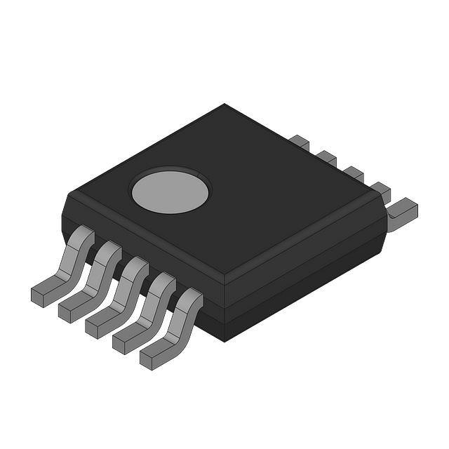
DGQ PACKAGE(4).(5)
(TOP VIEW)
ILIM
FB
COMP
SS/SD
GND
1
10
2
9
3
8
4
7
5
6
BOOT
HDRV
SW
VDD
LDRV
ACTUAL SIZE
3,05mm x 4,98mm
(4)
(5)
2
See technical brief SLMA002 for PCB guidelines for PowerPAD packages.
PowerPADt heat slug can be connected to GND (pin 5).
www.ti.com
���������� ��������
��������� �������
��������� �������
SLUS507D − JANUARY 2002 − REVISED NOVEMBER 2005
ELECTRICAL CHARACTERISTICS
over recommended operating temperature range, TA = −40_C to 85_C, VDD = 5.0 V, all parameters measured at zero
power dissipation (unless otherwise noted)
input supply
PARAMETER
VDD
VHGATE
IDD
UVLO
TEST CONDITIONS
Input voltage range
MIN
TYP
MAX
2.25
High-side gate voltage
UNIT
5.5
5.5
V
Shutdown current
VBOOT − VSW
SS/SD = 0 V,
0.25
0.45
Quiescent current
FB = 0.8 V
1.4
2.0
Switching current
No load at HDRV/LDRV
1.5
4.0
1.95
2.05
2.15
V
80
140
200
mV
Outputs off
Minimum on-voltage
Hysteresis
mA
oscillator
PARAMETER
TEST CONDITIONS
TPS40000
TPS40001
TPS40004
fOSC
VRAMP
Oscillator frequency
TPS40002
TPS40003
TPS40005
Ramp voltage
MIN
TYP
250
MAX
300
350
2.25 V ≤ VDD ≤ 5.00 V
VPEAK − VVALLEY
Ramp valley voltage
UNIT
kHz
500
600
700
0.80
0.93
1.07
0.24
0.31
0.41
V
PWM
PARAMETER
Maximum duty cycle(2)
TEST CONDITIONS
TPS40000
TPS40001
TPS40004
TPS40002
TPS40003
TPS40005
FB = 0 V,
MIN
TYP
MAX
87%
94%
97%
83%
93%
97%
UNIT
VDD = 3.3 V
Minimum duty cycle
0%
error amplifier
PARAMETER
TEST CONDITIONS
Line,
VFB
FB input voltage
Temperature
TA = 25°C
MIN
TYP
0.689
0.700
0.711
0.693
0.700
0.707
30
130
2.0
2.5
FB input bias current
UNIT
V
nA
VOH
VOL
High-level output voltage
FB = 0 V,
Low-level output voltage
FB =VDD,
IOH
IOL
Output source current
COMP = 0.7 V,
FB = GND
2
6
Output sink current
Gain bandwidth(1)
COMP = 0.7 V,
FB = VDD
3
8
5
10
MHz
55
85
dB
GBW
IOH = 0.5 mA
IOL = 0.5 mA
MAX
AOL
Open loop gain
(1) Ensured by design. Not production tested.
(2) At VDD input voltage of 2.25 V, derate the maximum duty cycle by 3%.
www.ti.com
0.08
0.15
V
mA
3
���������� ��������
��������� �������
��������� �������
SLUS507D − JANUARY 2002 − REVISED NOVEMBER 2005
ELECTRICAL CHARACTERISTICS
over recommended operating temperature range, TA = −40_C to 85_C, VDD = 5.0 V, all parameters measured at zero
power dissipation (unless otherwise noted)
current limit
PARAMETER
TEST CONDITIONS
ISINK
ILIM sink current
VDD = 5 V
VDD = 2.25 V
VOS
VILIM
Offset voltage SW vs ILIM(1)
2.25 V ≤ VDD ≤ 5.00
tON
Minimum HDRV pulse time in overcurrent
MIN
TYP
15
19
9.5
13.0
16.5
−20
0
Input voltage range
2
VDD = 3.3 V
200
SW leading edge blanking pulse in overcurrent detection
20
UNIT
µA
A
mV
VDD
V
300
ns
100
Soft-start capacitor cycles as fault timer(1)
tSS
MAX
11
ns
6
rectifier zero current comparator
PARAMETER
VSW
Sense voltage to turn off
rectifier
TEST CONDITIONS
TPS40000
TPS40002
LDRV output OFF
MIN
−15
SW leading edge blanking pulse in zero
current detection
TYP
−7
MAX
−2
75
UNIT
mV
ns
predictive delay
PARAMETER
VSWP
TLDHD
THDLD
TEST CONDITIONS
MIN
Sense threshold to modulate delay time
TYP
MAX
−350
UNIT
mV
Maximum delay modulation range time
LDRV OFF − to − HDRV ON
50
75
100
ns
Predictive counter delay time per bit
LDRV OFF − to − HDRV ON
3.0
4.5
6.2
ns
Maximum delay modulation range
HDRV OFF − to − LDRV ON
40
65
90
ns
Predictive counter delay time per bit
HDRV OFF − to − LDRV ON
2.4
4.0
5.6
ns
shutdown
PARAMETER
VSD
VEN
Shutdown threshold voltage
TEST CONDITIONS
Outputs OFF
Device active threshold voltage
MIN
TYP
MAX
UNIT
0.09
0.13
0.205
V
0.14
0.17
0.235
V
soft start
PARAMETER
ISS
VSS
Soft-start source current
TEST CONDITIONS
Outputs OFF
Soft-start clamp voltage
MIN
TYP
MAX
UNIT
2.0
3.7
5.4
µA
1.1
1.5
1.9
V
bootstrap
PARAMETER
RBOOT
Bootstrap switch resistance
TEST CONDITIONS
VDD = 3.3 V
VDD = 5 V
(1)
Ensured by design. Not production tested.
(2)
At VDD input voltage of 2.25 V, derate the maximum duty cycle by 3%.
4
www.ti.com
MIN
TYP
MAX
50
100
35
70
UNIT
Ω
���������� ��������
��������� �������
��������� �������
SLUS507D − JANUARY 2002 − REVISED NOVEMBER 2005
ELECTRICAL CHARACTERISTICS
over recommended operating temperature range, TA = −40_C to 85_C, VDD = 5.0 V, all parameters measured at zero
power dissipation (unless otherwise noted)
output driver
PARAMETER
TEST CONDITIONS
RHDHI
HDRV pull-up resistance
VBOOT−VSW = 3.3 V,
ISOURCE = −100 mA
RHDLO
HDRV pull-down resistance
VBOOT − VSW = 3.3 V,
ISINK = 100 mA
RLDHI
LDRV pull-up resistance
RLDLO
LDRV pull-down resistance
tRISE
tFALL
ISOURCE = −100 mA
ISINK = 100 mA
TYP
MAX
UNIT
3
5.5
1.5
3
3
5.5
1.0
2.0
LDRV rise time
15
35
LDRV fall time
10
25
15
35
10
25
HDRV rise time
VDD = 3.3 V,
VDD = 3.3 V,
MIN
CLOAD = 1 nF
HDRV fall time
Ω
ns
thermal shutdown
PARAMETER
TEST CONDITIONS
MIN
Shutdown temperature(1)
Hysteresiss(1)
tSD
TYP
MAX
165
UNIT
°C
15
sw node
PARAMETER
TEST CONDITIONS
Leakage current in shutdown (1)
ISW
(1) Ensured by design. Not production tested.
(2)
MIN
TYP
15
MAX
UNIT
µA
At VDD input voltage of 2.25 V, derate the maximum duty cycle by 3%.
www.ti.com
5
���������� ��������
��������� �������
��������� �������
SLUS507D − JANUARY 2002 − REVISED NOVEMBER 2005
Terminal Functions
TERMINAL
I/O
DESCRIPTION
NAME
NO.
BOOT
10
O
Provides a bootstrapped supply for the topside MOSFET driver, enabling the gate of the topside
MOSFET to be driven above the input supply rail
COMP
3
O
Output of the error amplifier
FB
2
I
Inverting input of the error amplifier. In normal operation the voltage at this pin is the internal reference level of 700 mV.
GND
5
−
Power supply return for the device. The power stage ground return on the board requires a separate path from other
sensitive signal ground returns.
HDRV
9
O
This is the gate drive output for the topside N-channel MOSFET. HDRV is bootstrapped to near 2×VDD for good enhancement of the topside MOSFET.
ILIM
1
I
A resistor is connected between this pin and VDD to set up the over current threshold voltage. A 15-µA current sink at
the pin establishes a voltage drop across the external resistor that represents the drain-to-source voltage across the
top side N-channel MOSFET during an over current condition. The ILIM over current comparator is blanked for the
first 100 ns to allow full enhancement of the top
MOSFET. Set the ILIM voltage level such that it is within 800 mV of VDD; that is, (VDD − 0.8) ≤ IILIM ≤ VDD.
LDRV
6
O
Gate drive output for the low-side synchronous rectifier N-channel MOSFET
I
Soft-start and overcurrent fault shutdown times are set by charging and discharging a capacitor connected to this pin.
A closed loop soft-start occurs when the internal 3-µA current source charges the external capacitor from 0.17 V to
0.70 V. During the soft-start period, the current sink capability of the TPS40001 and TPS40003 is disabled. When the
SS/SD voltage is less than 0.12 V, the device is shutdown and the HDRV and LDRV are driven low. In normal operation, the capacitor is charged to 1.5 V. When a fault condition is asserted, the HDRV is driven low, and the LDRV is
driven high. The soft-start capacitor goes through six charge/discharge cycles, restarting the converter on the seventh
cycle.
SS/SD
4
SW
8
O
Connect to the switched node on the converter. This pin is used for overcurrent sensing in the topside N-channel
MOSFET, zero current sensing in synchronous rectifier N-channel MOSFET, and level sensing for predictive delay
circuit. Overcurrent is determined, when the topside N-channel MOSFET is on, by comparing the voltage on SW with
respect to VDD and the voltage on the ILIM with respect to VDD. Zero current is sensed, when the rectifier N-channel
MOSFET is on, by measuring the voltage on SW with respect to ground. Zero current sensing applies to the
TPS40000/2 devices only.
VDD
7
I
Power input for the chip, 5.5-V maximum. Decouple close to the pin with a low-ESR capacitor, 1-µF or larger.
6
www.ti.com
���������� ��������
��������� �������
��������� �������
SLUS507D − JANUARY 2002 − REVISED NOVEMBER 2005
functional block diagram
VDD
VDD
7
VDD
ERROR AMPLIFIER
2
0.7 V
+
+
UVLO
SS ACTIVE
SOFT
START
PWM
CLK
3
4
GND
BOOT
9
HDRV
PWM
LOGIC
8
SW
6
LDRV
1
ILIM
PREDICTIVE
GATE
DRIVE
(VDD−1.2 V)
FAULT
FAULT
COUNTER
OC
VDD
DISCHARGE
0.12 V
10
UVLO
OSC
3 µA
SS/SD
PWM COMP
HI
REF
COMP
LDRV
UVLO
2V
FB
THERMAL
SHUTDOWN
100 ns DELAY
SHUT DOWN
LO
EN
CURRENT
LIMIT COMP
5
15 µA
LDRV
EN
75 ns
DELAY
RECTIFIER
ZERO−CURRENT
COMPARATOR
UDG−01142
www.ti.com
7
���������� ��������
��������� �������
��������� �������
SLUS507D − JANUARY 2002 − REVISED NOVEMBER 2005
APPLICATION INFORMATION
The TPS4000x series of synchronous buck controller devices is optimized for high-efficiency dc-to-dc
conversion in non-isolated distributed power systems. A typical application circuit is shown in Figure 1.
The TPS40004 and TPS40005 are the controllers of choice for most general purpose synchronous buck
designs. Each operates in two quadrant mode (i.e. source or sink current) full time. This choice provides the
best performance for output voltage load transient response over the widest load current range.
The TPS40001 and TPS40003 add an additional feature: They operate in single quadrant mode (i.e. source
current only) during converter startup, and then when the converter has reached the regulation point, the
controllers change to operate in two quadrant mode. This is useful for applications that have outputs pre-biased
at some voltage before the controller is enabled. When the TPS40001 or TPS40003 is enabled, it does not sink
current during startup and therefore does not pull current from the pre-biased voltage supply.
The TPS40000 and TPS40002 operate in single quadrant mode (source current only) full time, allowing the
paralleling of converters. Single quadrant operation ensures one converter does pull current from a paralleled
converter. A converter using one of these controllers emulates a non-synchronous buck converter at light loads.
When current in the output inductor attempts to reverse, an internal zero-current detection circuit turns OFF the
synchronous rectifier and causes the current flow in the inductor to become discontinuous. At average load
currents greater than the peak amplitude of the inductor ripple current, the converter returns to operation as a
synchronous buck converter to maximize efficiency.
VDD
3.0 V to 5.5 V
100 µF
10 µF
20 kW
TPS40001
1
ILIM
BOOT 10
Si4836DY
3.6 nF
2
FB
3
COMP
HDRV 9
7.68 kΩ
VOUT 1.8 V
10 A
IHLP5050CE−01
1.0 µH
3.3 Ω
SW 8
100 nF
243 Ω
100 pF
4
SS/SD
VDD 7
Si4836DY
470 µF
10 µF
15.7 kΩ
3.3 nF
4.7 nF
5
GND
LDRV 6
10 kΩ
UDG−02013
Figure 1. Typical Application Circuit
8
www.ti.com
���������� ��������
��������� �������
��������� �������
SLUS507D − JANUARY 2002 − REVISED NOVEMBER 2005
APPLICATION INFORMATION
error amplifier
The error amplifier has a bandwidth of greater than 5 MHz, with open loop gain of at least 55 dB. The COMP
output voltage is clamped to a level above the oscillator ramp in order to improve large-scale transient response.
oscillator
The oscillator uses an internal resistor and capacitor to set the oscillation frequency. The ramp waveform is a
triangle at the PWM frequency with a peak voltage of 1.25 V, and a valley of 0.25 V. The PWM duty cycle is limited
to a maximum of 95%, allowing the bootstrap capacitor to charge during every cycle.
bootstrap/charge pump
There is an internal switch between VDD and BOOT. This switch charges the external bootstrap capacitor for
the floating supply. If the resistance of this switch is too high for the application, an external schottky diode
between VDD and BOOT can be used. The peak voltage on the bootstrap capacitor is approximately equal to
VDD.
driver
The HDRV and LDRV MOSFET drivers are capable of driving gate-to-source voltages up to 5.5 V. At VIN, = 5 V
and using appropriate MOSFETs, a 20-A converter can be achieved. The LDRV driver switches between VDD
and ground, while the HDRV driver is referenced to SW and switches between BOOT and SW. The maximum
voltage between BOOT and SW is 5.5 V.
synchronous rectification and predictive delay
In a normal buck converter, when the main switch turns off, current is flowing to the load in the inductor. This
current cannot be stopped immediately without using infinite voltage. For the current path to flow and maintain
voltage levels at a safe level, a rectifier or catch device is used. This device can be either a conventional diode,
or it can be a controlled active device if a control signal is available to drive it. The TPS4000x provides a signal
to drive an N-channel MOSFET as a rectifier. This control signal is carefully coordinated with the drive signal
for the main switch so that there is minimum delay from the time that the rectifier MOSFET turns off and the main
switch turns on, and minimum delay from when the main switch turns off and the rectifier MOSFET turns on.
This scheme, Predictive Gate Drivet delay, uses information from the current switching cycle to adjust the
delays that are to be used in the next cycle. Figure 2 shows the switch-node voltage waveform for a
synchronously rectified buck converter. Illustrated are the relative effects of a fixed-delay drive scheme
(constant, pre-set delays for the turn-off to turn-on intervals), an adaptive delay drive scheme (variable delays
based upon voltages sensed on the current switching cycle) and the predictive delay drive scheme.
Note that the longer the time spent in diode conduction during the rectifier conduction period, the lower the
efficiency. Also, not described in Figure 2 is the fact that the predictive delay circuit can prevent the body diode
from becoming forward biased at all while at the same time avoiding cross conduction or shoot through. This
results in a significant power savings when the main MOSFET turns on, and minimizes reverse recovery loss
in the body diode of the rectifier MOSFET.
www.ti.com
9
���������� ��������
��������� �������
��������� �������
SLUS507D − JANUARY 2002 − REVISED NOVEMBER 2005
APPLICATION INFORMATION
GND
Channel Conduction
Body Diode Conduction
Fixed Delay
Adaptive Delay
Predictive Delay
UDG−01144
Figure 2. Switch Node Waveforms for Synchronous Buck Converter
overcurrent
Overcurrent conditions in the TPS4000x are sensed by detecting the voltage across the main MOSFET while
it is on.
basic description
If the voltage exceeds a pre-set threshold, the current pulse is terminated, and a counter inside the device is
incremented. If this counter fills up, a fault condition is declared and the device disables switching for a period
of time and then attempts to restart the converter with a full soft-start cycle.
10
www.ti.com
���������� ��������
��������� �������
��������� �������
SLUS507D − JANUARY 2002 − REVISED NOVEMBER 2005
APPLICATION INFORMATION
detailed description
During each switching cycle, a comparator looks at the voltage across the top side MOSFET while it is on. This
comparator is enabled after the SW node reaches a voltage greater than (VDD−1.2 V) followed by a 100-ns
blanking time. If the voltage across that MOSFET exceeds a programmable threshold voltage, the
current-switching pulse is terminated and a 3-bit counter is incremented by one count. If, during the switching
cycle, the topside MOSFET voltage does not exceed a preset threshold, then this counter is decremented by
one count. (The counter does not wrap around from 7 to 0 or from 0 to 7). If the counter reaches a full count
of 7, the device declares that a fault condition exists at the output of the converter. In this fault state, HDRV is
turned off and LDRV is turned on and the soft-start capacitor is discharged. The counter is decremented by one
by the soft start capacitor (CSS) discharge. When the soft-start capacitor is fully discharged, the discharging
circuit is turned off and the capacitor is allowed to charge up at the nominal charging rate. When the soft-start
capacitor reaches about 700 mV, it is discharged again and the overcurrent counter is decremented by one
count. The capacitor is charged and discharged, and the counter decremented until the count reaches zero (a
total of six times). When this happens, the outputs are again enabled as the soft-start capacitor generates a
reference ramp for the converter to follow while attempting to restart.
During this soft-start interval (whether or not the controller is attempting to do a fault recovery or starting for the
first time), pulse-by-pulse current limiting is in effect, but overcurrent pulses are not counted to declare a fault
until the soft-start cycle has been completed. It is possible to have a supply attempt to bring up a short circuit
for the duration of the soft start period plus seven switching cycles. Power stage designs should take this into
account if it makes a difference thermally. Figure 3 shows the details of the overcurrent operation.
(+)
VTS
(−)
Overcurrent
Threshold
Voltage
Internal PWM
VTS
0V
External
Main Drive
Normal
Cycle
Overcurrent
Cycle
UDG−01145
Figure 3. Switch Node Waveforms for Synchronous Buck Converter
www.ti.com
11
���������� ��������
��������� �������
��������� �������
SLUS507D − JANUARY 2002 − REVISED NOVEMBER 2005
APPLICATION INFORMATION
Figure 4 shows the behavior of key signals during initial startup, during a fault and a successfully fault recovery.
At time t0, power is applied to the converter. The voltage on the soft-start capacitor (VCSS) begins to ramp up
and acts as the reference until it passes the internal reference voltage at t1. At this point the soft-start period
is over and the converter is regulating its output at the desired voltage level. From t0 to t1, pulse-by-pulse current
limiting is in effect, and from t1 onward, overcurrent pulses are counted for purposes of determining a possible
fault condition. At t2, a heavy overload is applied to the converter. This overload is in excess of the overcurrent
threshold. The converter starts limiting current and the output voltage falls to some level depending on the
overload applied. During the period from t2 to t3, the counter is counting overcurrent pulses, and at time t3
reaches a full count of 7. The soft-start capacitor is then discharged, the counter is decremented, and a fault
condition is declared.
0.7 V
VCSS
FAULT
ILOAD
VOUT
t
t0
t1
t4
t2 t3
0
6
t5
5
t6
4
t7
3
t8
2
t9
1
t10
0
1 2 3 4 5 6 7
UDG−01144
Figure 4. Switch Node Waveforms for Synchronous Buck Converter
When the soft start capacitor is fully discharged, it begins charging again at the same rate that it does on startup,
with a nominal 3-µA current source. As the capacitor voltage reaches full charge, it is discharged again and the
counter is decremented by one count. These transitions occur at t3 through t9. At t9, the counter has been
decremented to 0. The fault logic is then cleared, the outputs are enabled, and the converter attempts to restart
with a full soft-start cycle. The converter comes into regulation at t10.
12
www.ti.com
���������� ��������
��������� �������
��������� �������
SLUS507D − JANUARY 2002 − REVISED NOVEMBER 2005
APPLICATION INFORMATION
setting the current limit
Connecting a resistor from VDD to ILIM sets the current limit. A 15-µA current sink internal to the device causes
a voltage drop at ILIM that is equal to the overcurrent threshold voltage. Ensure that (VDD−0.8 V) ≤ VILIM ≤ VDD.
The tolerance of the current sink is too loose to do an accurate current limit. The main purpose is for hard fault
protection of the power switches. Given the tolerance of the ILIM sink current, and the RDS(on) range for a
MOSFET, it is generally possible to apply a load that thermally damages the converter. This device is intended
for embedded converters where load characteristics are defined and can be controlled.
soft-start and shutdown
These two functions are common to the SS/SD pin. The voltage at this pin is the controlling voltage of the error
amplifier during startup. This reduces the transient current required to charge the output capacitor at startup,
and allows for a smooth startup with no overshoot of the output voltage if done properly. A shutdown feature
can be implemented as shown in Figure 5.
TPS40000
3 µA
4
CSS
SS/SD
SHUTDOWN
UDG−01143
Figure 5. Shutdown Implementation
The device shuts down when the voltage at the SS/SD pin falls below 120 mV. Because of this limitation, it is
recommended that a MOSFET be used as the controlling device, as in Figure 5. An open-drain CMOS logic
output would work equally well.
rectifier zero-current
Both the TPS40000 and TPS40002 parts are source-only, thus preventing reverse current in the synchronous
rectifier. Synchronous rectification is terminated by sensing the voltage, SW with respect to ground, across the
low-side MOSFET. When SW node is greater than −7 mV, rectification is terminated and stays off until the next
PWM cycle. In order to filter out undesired noise on the SW node, the zero-current comparator is blanked for
75 ns from the time the rectifier is turned on.
The TPS40001 and TPS40003 parts enable the zero-current comparator, (and therefore prevent reverse
current), while soft-start is active. However, when the output reaches regulation; that is, at the end of the
soft-start time, this comparator is disabled to allow the synchronous rectifier to sink current.
www.ti.com
13
���������� ��������
��������� �������
��������� �������
SLUS507D − JANUARY 2002 − REVISED NOVEMBER 2005
APPLICATION INFORMATION
The following pages include design ideas for a few applications. For more ideas, detailed design information,
and helpful hints, visit the TPS40000 resources at http://power.ti.com.
VDD
3.3 V
22 µF
TPS40002/3/5
15 kΩ
1 nF
22 µF
1
ILIM
BOOT 10
2
FB
HDRV
FDS6894A
1.0 µH
9
8.66 kΩ
3.3 Ω
3
COMP
SW
8
4
SS/SD
VDD
7
5
GND
LDRV
6
VOUT
1.2 V
5A
1 µF
2.2 Ω
68 pF
22 µF
22 µF
FDS6894A
.0033 µF
4.7 nF
PWP
1 µF
12.1 kΩ
470 pF
1 kΩ
16.9 kΩ
UDG−02081
Figure 6. Small-Form Factor Converter for 3.3 V to 1.2 V at 5 A.
14
www.ti.com
�+
82 pF
6.19 kΩ
C14
4.7 nF
330 µF
11 kΩ
330 µF
2.2 nF
+
VDD
3.3 V
www.ti.com
LDRV
VDD
SW
HDRV
6
7
8
9
1 µF
1.8 Ω
3.3 Ω
1.8 Ω
1 µF
22 µF
BOOT 10
PWP
GND
SS/SD
4
5
COMP
FB
2
3
ILIM
1
TPS40000/1/4
22 µF
Si4866DY
Si4866DY
1.5 µH
10 nF
2.2 Ω
22 µF
22 µF
14 kW
22 µF
392 Ω
10 kΩ
22 µF
22 µF
UDG−02082
1200 pF
VOUT
1.2 V
10 A
��������� ��������
��������� �������
��������� �������
SLUS507D − JANUARY 2002 − REVISED NOVEMBER 2005
APPLICATION INFORMATION
Figure 7. High-Current Converter for 3.3 V to 1.2 V at 10 A.
15
���������� ��������
��������� �������
��������� �������
SLUS507D − JANUARY 2002 − REVISED NOVEMBER 2005
APPLICATION INFORMATION
22 µF
VDD
2.5 V
22 µF
BAT54
15 kΩ
TPS40002/3/5
1 µF
1
ILIM
BOOT 10
2
FB
HDRV
9
3
COMP
SW
8
4
SS/SD
VDD
7
FDS6894A
1.8 Ω
1500 pF
5.62 kΩ
100 pF
1.0 µH
L1
VOUT
1.2 V
5A
3.3 Ω
4.7 nF
2.2 Ω
1.8 Ω
5
GND LDRV
PWP
6
22 µF
FDS6894A
22 µF
3.3 nF
1 µF
6.19 kΩ
536 Ω
1000 pF
8.66 kΩ
UDG−02083
Figure 8. Ultra-Low-Input Voltage Converter for 2.5 V to 1.2 V at 5 A
16
www.ti.com
���������� ��������
��������� �������
��������� �������
SLUS507D − JANUARY 2002 − REVISED NOVEMBER 2005
APPLICATION INFORMATION
+
VDD
3.3 V
330 µF +
330 µF
22 µF
22 µF
TPS40000/1/4
11 kΩ
1 µF
1
ILIM
BOOT 10
2
FB
HDRV
9
3
COMP
SW
8
4
SS/SD
VDD
7
22 µF
Q1
Si4866DY
1.8 Ω
1.0 µH
L2
VOUT
2.5 V
10 A
3.3 Ω
2.2 nF 12.7 kΩ
2.2 Ω
470 pF
4.7 nF
1.8 Ω
5
GND LDRV
PWP
Q2
Si4866DY
6
1 µF
0.01 µF
+
22 µF
22 µF 470 µF
24.9 kΩ
820 pF
1.27 kΩ
9.76 kΩ
UDG−02084
Figure 9. Ultra-High-Efficiency Converter for 3.3 V to 2.5 V at 10 A
www.ti.com
17
���������� ��������
��������� �������
��������� �������
SLUS507D − JANUARY 2002 − REVISED NOVEMBER 2005
TYPICAL CHARACTERISTICS
OSCILLATOR FREQUENCY PERCENT CHANGE
vs
INPUT VOLTAGE
OSCILLATOR FREQUENCY PERCENT CHANGE
vs
TEMPERATURE
∆fOSC − Change in Oscillator Frequency − %
∆fOSC − Change in Oscillator Frequency − %
6
5
4
3
2
1
0
2.0
2.5
3.0
3.5
4.0
4.5
5.0
5.5
1
0
−1
−2
−3
−4
−5
−6
−50
−25
0
25
50
75
100
125
Temperature − °C
VIN − Input Voltage − V
Figure 11
Figure 10
FEEDBACK VOLTAGE
vs
INPUT VOLTAGE
FEEDBACK VOLTAGE
vs
TEMPERATURE
0.707
0.7010
0.7005
VFB − Feedback Voltage − V
VFB − Feedback Voltage − V
0.705
0.7000
0.6995
0.703
0.701
0.699
0.697
0.695
0.6990
2.0
2.5
3.0
3.5
4.0
4.5
5.0
5.5
0.693
VIN − Input Voltage − V
Figure 12
18
−50
−25
0
25
50
Temperature − °C
Figure 13
www.ti.com
75
100
125
���������� ��������
��������� �������
��������� �������
SLUS507D − JANUARY 2002 − REVISED NOVEMBER 2005
TYPICAL CHARACTERISTICS
CURRENT LIMIT SINK CURRENT
vs
INPUT VOLTAGE
CURRENT LIMIT SINK CURRENT
vs
TEMPERATURE
16.0
15.0
ILIMIT − Sink Current Limit − µA
ILIMIT − Sink Current Limit − µA
15.5
14.5
14.0
13.5
15.5
15.0
14.5
13.0
12.5
14.0
2.0
2.5
3.0
3.5
4.0
4.5
5.0
5.5
−50
−25
0
25
50
75
100
125
Temperature − °C
VIN − Input Voltage − V
Figure 14
Figure 15
OVERCURRENT
TYPICAL PREDICTIVE
DELAY SWITCHING
SS/SD Node
(1 V/div)
LDRV
(2 V/div)
SW Node
SW Node
(2 V/ div)
(2 V/ div)
t − Time − 1 ms/div
t − Time − 400 ns/div
Figure 16
Figure 17
www.ti.com
19
�PACKAGE OPTION ADDENDUM
www.ti.com
14-Oct-2022
PACKAGING INFORMATION
Orderable Device
Status
(1)
Package Type Package Pins Package
Drawing
Qty
Eco Plan
(2)
Lead finish/
Ball material
MSL Peak Temp
Op Temp (°C)
Device Marking
(3)
Samples
(4/5)
(6)
TPS40000DGQ
ACTIVE
HVSSOP
DGQ
10
80
RoHS & Green
NIPDAUAG
Level-1-260C-UNLIM
-40 to 85
40000
Samples
TPS40000DGQR
ACTIVE
HVSSOP
DGQ
10
2500
RoHS & Green
NIPDAUAG
Level-1-260C-UNLIM
-40 to 85
40000
Samples
TPS40001DGQ
NRND
HVSSOP
DGQ
10
80
RoHS & Green
NIPDAU
Level-1-260C-UNLIM
-40 to 85
40001
TPS40001DGQR
NRND
HVSSOP
DGQ
10
2500
RoHS & Green
NIPDAU
Level-2-260C-1 YEAR
-40 to 85
40001
TPS40002DGQ
NRND
HVSSOP
DGQ
10
80
RoHS & Green
NIPDAU
Level-1-260C-UNLIM
-40 to 85
40002
TPS40002DGQR
NRND
HVSSOP
DGQ
10
2500
RoHS & Green
NIPDAU
Level-1-260C-UNLIM
-40 to 85
40002
TPS40003DGQ
NRND
HVSSOP
DGQ
10
80
RoHS & Green
NIPDAU
Level-1-260C-UNLIM
-40 to 85
40003
TPS40003DGQR
NRND
HVSSOP
DGQ
10
2500
RoHS & Green
NIPDAU
Level-2-260C-1 YEAR
-40 to 85
40003
TPS40005DGQR
NRND
HVSSOP
DGQ
10
2500
RoHS & Green
NIPDAU
Level-1-260C-UNLIM
-40 to 85
40005
(1)
The marketing status values are defined as follows:
ACTIVE: Product device recommended for new designs.
LIFEBUY: TI has announced that the device will be discontinued, and a lifetime-buy period is in effect.
NRND: Not recommended for new designs. Device is in production to support existing customers, but TI does not recommend using this part in a new design.
PREVIEW: Device has been announced but is not in production. Samples may or may not be available.
OBSOLETE: TI has discontinued the production of the device.
(2)
RoHS: TI defines "RoHS" to mean semiconductor products that are compliant with the current EU RoHS requirements for all 10 RoHS substances, including the requirement that RoHS substance
do not exceed 0.1% by weight in homogeneous materials. Where designed to be soldered at high temperatures, "RoHS" products are suitable for use in specified lead-free processes. TI may
reference these types of products as "Pb-Free".
RoHS Exempt: TI defines "RoHS Exempt" to mean products that contain lead but are compliant with EU RoHS pursuant to a specific EU RoHS exemption.
Green: TI defines "Green" to mean the content of Chlorine (Cl) and Bromine (Br) based flame retardants meet JS709B low halogen requirements of