TPS40170-EP
www.ti.com
SLVSBT7A – MARCH 2013 – REVISED APRIL 2013
4.5-V TO 60-V WIDE-INPUT SYNCHRONOUS PWM BUCK CONTROLLER
Check for Samples: TPS40170-EP
FEATURES
1
•
•
•
•
2
•
•
•
•
•
•
•
•
•
•
•
•
Wide-Input Voltage Range from 4.5 V to 60 V
600-mV Reference Voltage With 1% Accuracy
Programmable UVLO and Hysteresis
Voltage-Mode Control With Voltage FeedForward
Programmable Frequency Between 100 kHz
and 600 kHz
Bidirectional Frequency Synchronization With
Master/Slave Option
Low-Side FET Sensing Overcurrent Protection
and High-Side FET Sensing Short-Circuit
Protection With Integrated Thermal
Compensation
Programmable Closed-Loop Soft-Start
Supports Pre-Biased Outputs
Thermal Shutdown at 165°C With Hysteresis
Voltage Tracking
Power Good
ENABLE With 1-µA Low-Current Shutdown
8-V and 3.3-V LDO Output
Integrated Bootstrap Diode
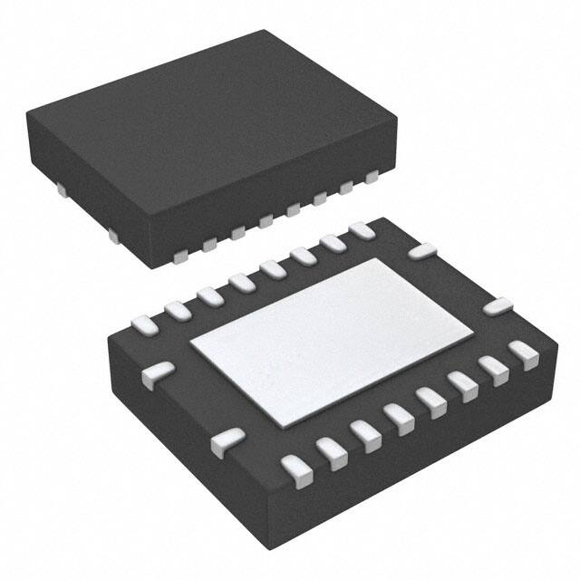
20-Pin 3.5-mm × 4.5-mm QFN (RGY) Package
APPLICATIONS
•
•
POL Modules
Wide Input Voltage, High-Power-Density
DC/DC Converter
SUPPORTS DEFENSE, AEROSPACE,
AND MEDICAL APPLICATIONS
•
•
•
•
•
•
•
Controlled Baseline
One Assembly and Test Site
One Fabrication Site
Available in Military (–55°C to 125°C)
Temperature Range
Extended Product Life Cycle
Extended Product-Change Notification
Product Traceability
DESCRIPTION
TPS40170 is a full-featured, synchronous PWM buck
controller that operates at an input voltage between
4.5 V and 60 V and is optimized for high-powerdensity, high-reliability dc-dc converter applications.
The controller implements voltage-mode control with
input-voltage feed-forward compensation that enables
instant response to an input voltage change. The
switching frequency is programmable from 100 kHz to
600 kHz.
The TPS40170 has a complete set of system
protection and monitoring features such as
programmable UVLO, programmable overcurrent
protection (OCP) by sensing the low-side FET,
selectable short-circuit protection (SCP) by sensing
the high-side FET, and thermal shutdown. The
ENABLE pin allows for system shutdown in a lowcurrent (1-µA typical) mode. The controller supports
pre-biased output, provides an open-drain PGOOD
signal, and has closed-loop soft-start, output-voltage
tracking, and adaptive dead-time control.
TPS40170
provides
accurate
output-voltage
regulation within 1% accuracy. Additionally, the
controller implements a novel scheme of bidirectional
synchronization with one controller acting as the
master and other downstream controllers acting as
slaves, synchronized to the master in-phase or 180°
out-of-phase. Slave controllers can be synchronized
to an external clock within ±30% of the free-running
switching frequency.
1
2
Please be aware that an important notice concerning availability, standard warranty, and use in critical applications of
Texas Instruments semiconductor products and disclaimers thereto appears at the end of this data sheet.
NexFET is a trademark of Texas Instruments.
PRODUCTION DATA information is current as of publication date.
Products conform to specifications per the terms of the Texas
Instruments standard warranty. Production processing does not
necessarily include testing of all parameters.
Copyright © 2013, Texas Instruments Incorporated
�TPS40170-EP
SLVSBT7A – MARCH 2013 – REVISED APRIL 2013
www.ti.com
SIMPLIFIED APPLICATION
VIN
1
20
ENABLE
UVLO
2
SYNC
3
M/S
BOOT 18
4
RT
HDRV 17
5
SS
SW 16
VIN 19
VOUT
TPS40170
6
TRK
7
FB
8
COMP
9
AGND
VBP 15
LDRV 14
PGND 13
ILIM 12
VDD
PGOOD
10
11
UDG-09219
This integrated circuit can be damaged by ESD. Texas Instruments recommends that all integrated circuits be handled with
appropriate precautions. Failure to observe proper handling and installation procedures can cause damage.
ESD damage can range from subtle performance degradation to complete device failure. Precision integrated circuits may be more
susceptible to damage because very small parametric changes could cause the device not to meet its published specifications.
ORDERING INFORMATION (1)
(1)
2
TJ
PACKAGE
PINS
TRANSPORT MEDIA
QUANTITY
DEVICE NUMBER
TOP-SIDE
MARKING
VID NUMBER
–55°C to 125°C
QFN
20
Tape and reel
250
TPS40170MRGYTEP
PZYM
V62/13607-01XE
For the most current package and ordering information see the Package Option Addendum at the end of this document, or see the TI
web site at www.ti.com.
Submit Documentation Feedback
Copyright © 2013, Texas Instruments Incorporated
Product Folder Links :TPS40170-EP
�TPS40170-EP
www.ti.com
SLVSBT7A – MARCH 2013 – REVISED APRIL 2013
ABSOLUTE MAXIMUM RATINGS (1)
over operating free-air temperature range (unless otherwise noted)
VALUE
Input voltage
MIN
MAX
VIN
–0.3
62
M/S
–0.3
VIN
UVLO
–0.3
16
SW
–5
BOOT
Output voltage
Grounding
Electrostatic discharge (ESD)
UNIT
V
VIN
VSW + 8.8
HDRV
VSW
BOOT
BOOT-SW, HDRV-SW (differential from BOOT or
HDRV to SW)
–0.3
8.8
VBP, LDRV, COMP, RT, ENABLE, PGOOD, SYNC
–0.3
8.8
VDD, FB, TRK, SS, ILIM
–0.3
3.6
AGND-PGND, PGND-AGND
-200
200
V
PowerPAD to AGND (must be electrically connected
external to device)
0
mV
Human-body model (HBM)
1
kV
Charged-device model (CDM)
1
kV
Absolute maximum junction temperature TJ
-55
125
°C
Storage temperature
–55
150
°C
(1)
Tstg
Stresses beyond those listed under Absolute Maximum Ratings may cause permanent damage to the device. These are stress ratings
only, and functional operation of the device at these or any other conditions beyond those included under Recommended Operating
Conditions is not implied. Exposure to absolute-maximum-rated conditions for extended periods of time may affect device reliability.
THERMAL INFORMATION
TPS40170-EP
THERMAL METRIC
(1)
RGY
UNITS
20 PINS
θJA
Junction-to-ambient thermal resistance (2)
35.4
θJCtop
Junction-to-case (top) thermal resistance (3)
38.1
(4)
θJB
Junction-to-board thermal resistance
ψJT
Junction-to-top characterization parameter (5)
ψJB
Junction-to-board characterization parameter (6)
θJCbot
(1)
(2)
(3)
(4)
(5)
(6)
(7)
Junction-to-case (bottom) thermal resistance
10.8
°C/W
0.5
10.9
(7)
4.3
For more information about traditional and new thermal metrics, see the IC Package Thermal Metrics application report, SPRA953.
The junction-to-ambient thermal resistance under natural convection is obtained in a simulation on a JEDEC-standard, high-K board, as
specified in JESD51-7, in an environment described in JESD51-2a.
The junction-to-case (top) thermal resistance is obtained by simulating a cold plate test on the package top. No specific JEDECstandard test exists, but a close description can be found in the ANSI SEMI standard G30-88.
The junction-to-board thermal resistance is obtained by simulating in an environment with a ring cold plate fixture to control the PCB
temperature, as described in JESD51-8.
The junction-to-top characterization parameter, ψJT, estimates the junction temperature of a device in a real system and is extracted
from the simulation data for obtaining θJA, using a procedure described in JESD51-2a (sections 6 and 7).
The junction-to-board characterization parameter, ψJB, estimates the junction temperature of a device in a real system and is extracted
from the simulation data for obtaining θJA , using a procedure described in JESD51-2a (sections 6 and 7).
The junction-to-case (bottom) thermal resistance is obtained by simulating a cold plate test on the exposed (power) pad. No specific
JEDEC standard test exists, but a close description can be found in the ANSI SEMI standard G30-88.
Spacer
RECOMMENDED OPERATING CONDITIONS
over operating free-air temperature range (unless otherwise noted)
MIN
VIN
Input voltage
4.5
NOM
MAX
UNIT
60
Submit Documentation Feedback
Copyright © 2013, Texas Instruments Incorporated
Product Folder Links :TPS40170-EP
V
3
�TPS40170-EP
SLVSBT7A – MARCH 2013 – REVISED APRIL 2013
www.ti.com
ELECTRICAL CHARACTERISTICS
These specifications apply for –55ºC ≤ TJ ≤ +125ºC, VVIN = 12 V, unless otherwise noted.
PARAMETER
TEST CONDITIONS
MIN
TYP
MAX
UNIT
60
V
1
2.5
µA
4.5
mA
100
mV
INPUT SUPPLY
VVIN
Input voltage range
ISD
Shutdown current
VENABLE < 100 mV
4.5
IQQ
Operating current, drivers not switching
VENABLE ≥ 2 V, fSW = 300 kHz
ENABLE
VDIS
ENABLE pin voltage to disable the device
VEN
ENABLE pin voltage to enable the device
IENABLE
ENABLE pin source current
600
mV
410
nA
8.0
8.35
V
110
210
mV
8-V AND 3.3-V REGULATORS
VVBP
8-V regulator output voltage
VENABLE ≥ 2 V, 8.2 V < VVIN ≤ 60 V,
0 mA < IIN < 20 mA
VDO
8-V regulator dropout voltage,
VVIN-VVBP
4.5 < VVIN ≤ 8.2 V, VEN ≥ 2 V,
IIN = 10 mA
VVDD
3.3-V regulator output voltage
VENABLE ≥ 2 V, 4.5 V < VVIN ≤ 60 V,
0 mA < IIN < 5 mA
3.2
3.3
3.42
V
878
900
920
mV
4
5
6.2
µA
7.8
FIXED AND PROGRAMMABLE UVLO
VUVLO
Programmable UVLO ON voltage (at UVLO
pin)
VENABLE ≥ 2 V
IUVLO
Hysteresis current out of UVLO pin
VENABLE ≥ 2 V , UVLO pin > VUVLO
VBPON
VBP turnon voltage
VBPOFF
VBP turnoff voltage
VBPHYS
VBP UVLO Hysteresis voltage
VENABLE ≥ 2 V, UVLO pin > VUVLO
3.8
4.4
3.55
4.1
175
400
V
mV
REFERENCE
Reference voltage (+ input of the error
amplifier)
VREF
TJ = 25°C, 4.5 V < VVIN ≤ 60 V
594
600
606
–55°C ≤ TJ ≤ 125ºC, 4.5 V < VVIN ≤ 60 V
585
600
610
Range (typical)
100
mV
OSCILLATOR
fSW
Switching frequency
VVALLEY
Valley voltage
KPWM
PWM gain (VVIN / VRAMP)
600
RRT = 100 kΩ, 4.5 V 0.5 V
11.45
−60 −45 −30 −15 0 15 30 45 60 75 90 105 120 135
Junction Temperature (°C)
G011
Figure 12. Soft-Start Source Current vs Junction
Temperature (VSS > 0.5 V)
10
305
52.75
Temp Range: −55°C to 125°C
52.50
52.25
52.00
51.75
51.50
51.25
51.00
50.75
VSS < 0.5 V
50.50
−60 −45 −30 −15 0 15 30 45 60 75 90 105 120 135
Junction Temperature (°C)
G012
Figure 13. Soft-Start Source Current vs Junction
Temperature (VSS < 0.5 V)
Submit Documentation Feedback
Copyright © 2013, Texas Instruments Incorporated
Product Folder Links :TPS40170-EP
�TPS40170-EP
www.ti.com
SLVSBT7A – MARCH 2013 – REVISED APRIL 2013
TYPICAL CHARACTERISTICS (continued)
11.1
675
Temp Range: −55°C to 125°C
Soft-Start Initial Offset Voltage (mV)
ILIM Source Current (µA)
10.8
10.5
10.2
9.9
9.6
9.3
9.0
8.7
8.4
−60 −45 −30 −15 0 15 30 45 60 75 90 105 120 135
Junction Temperature (°C)
G013
Figure 14. ILIM Source Current vs Junction Temperature
Temp Range: −55°C to 125°C
665
655
645
635
625
615
605
595
−60 −45 −30 −15 0 15 30 45 60 75 90 105 120 135
Junction Temperature (°C)
G014
Figure 15. Soft-Start Initial Offset Voltage vs Junction
Temperature
Power Good Threshold Voltage (mV)
700
Temp Range: −55°C to 125°C
675
Overvoltage
Undervoltage
650
625
600
575
550
525
−60 −45 −30 −15 0 15 30 45 60 75 90 105 120 135
Junction Temperature (°C)
G015
Figure 16. VOV/VUV Power Good Threshold Voltage
Submit Documentation Feedback
Copyright © 2013, Texas Instruments Incorporated
Product Folder Links :TPS40170-EP
11
�TPS40170-EP
SLVSBT7A – MARCH 2013 – REVISED APRIL 2013
www.ti.com
APPLICATION INFORMATION
FUNCTIONAL DESCRIPTION
The TPS40170 is a synchronous PWM buck controller that accepts a wide range of input voltages from 4.5 V to
60 V and features voltage-mode control with input-voltage feed-forward compensation. The switching frequency
is programmable from 100 kHz to 600 kHz.
The TPS40170 has a complete set of system protections such as programmable UVLO, programmable
overcurrent protection (OCP), selectable short-circuit protection (SCP), and thermal shutdown. The ENABLE pin
allows for system shutdown in a low-current (1-µA typical) mode. The controller supports pre-biased outputs,
provides an open-drain PGOOD signal, and has closed-loop programmable soft-start, output-voltage tracking,
and adaptive dead-time control.
The TPS40170 provides accurate output voltage regulation within 1% accuracy.
Additionally, the controller implements a novel scheme of bidirectional synchronization with one controller acting
as the master and other downstream controllers acting as slaves, synchronized to the master in-phase or 180°
out-of-phase. Slave controllers can be synchronized to an external clock within ±30% of the internal switching
frequency.
LDO Linear Regulators and Enable
The TPS40170 has two internal low-dropout (LDO) linear regulators. One has a nominal output voltage of VVBP
and is present at the VBP pin. This is the voltage that is mainly used for the gate-driver output. The other linear
regulator has an output voltage of VVDD and is present at the VDD pin. This voltage can be used in external lowcurrent logic circuitry. The maximum allowable current drawn from the VDD pin must not exceed 5 mA.
The TPS40170 has a dedicated device-enable pin (ENABLE). This simplifies user-level interface design because
no multiplexed functions exist. If the ENABLE pin of the TPS40170 is higher than VEN, then the LDO regulators
are enabled. To ensure that the LDO regulators are disabled, the ENABLE pin must be pulled below VDIS. By
pulling the ENABLE pin below VDIS, the device is completely disabled and the current consumption is very low
(nominally, 1 µA). Both LDO regulators are actively discharged when the ENABLE pin is pulled below VDIS. A
functionally equivalent circuit to the enable circuitry on the TPS40170 is shown in Figure 17.
VIN
19
TPS40170
Always Active
ISD= 1 mA
ENABLE
1
+
DISABLE
+
VDIS
AGND
9
UDG-09147
Figure 17. TPS40170 ENABLE Functional Block
The ENABLE pin must not be allowed to float. If the ENABLE function is not needed for the design, then it is
suggested that the ENABLE pin be pulled up to VIN by a high-value resistor, ensuring that the current into the
ENABLE pin does not exceed 10 µA. If it is not possible to meet this clamp current requirement, then it is
suggested that a resistor divider from VIN to GND be used to connect to ENABLE pin. The resistor divider should
be such that the ENABLE pin is higher than VEN and lower than 8 V.
12
Submit Documentation Feedback
Copyright © 2013, Texas Instruments Incorporated
Product Folder Links :TPS40170-EP
�TPS40170-EP
www.ti.com
SLVSBT7A – MARCH 2013 – REVISED APRIL 2013
NOTE
To avoid potential erroneous behavior of the enable function, the ENABLE signal applied
must have a minimum slew rate of 20 V/s.
Input Undervoltage Lockout (UVLO)
The TPS40170 has both fixed and programmable input undervoltage lockout (UVLO). In order for the device to
turn ON, all of the following conditions must be met:
• The ENABLE pin voltage must be greater than VEN.
• The VBP voltage (at VBP pin) must be greater than VVBP(on).
• The UVLO pin must be greater than VUVLO.
In
•
•
•
order for the device to turn OFF, any one of the following conditions must be met:
The ENABLE pin voltage must be less than VDIS.
The VBP voltage (at the VBP pin) must be less than VVBP(off).
The UVLO pin must be less than VUVLO.
Programming the input UVLO can be accomplished using the UVLO pin. A resistor divider from the input voltage
(VIN pin) to GND sets the UVLO level. Once the input voltage reaches a value that meets the VUVLO level at the
UVLO pin, then a small hysteresis current, IUVLO at the UVLO pin is switched in. The programmable UVLO
function is shown in Figure 18.
VIN
TPS40170
IUVLO
R1
UVLO
+
20
R2
VIN_OK
1 nF
+
VUVLO
AGND
9
UDG-09199
Figure 18. UVLO Functional Block Schematic
Submit Documentation Feedback
Copyright © 2013, Texas Instruments Incorporated
Product Folder Links :TPS40170-EP
13
�TPS40170-EP
SLVSBT7A – MARCH 2013 – REVISED APRIL 2013
www.ti.com
Equations for Programming the Input UVLO:
Components R1 and R2 represent external resistors for programming UVLO and hysteresis; their values can be
calculated in Equation 1 and Equation 2, respectively.
V - VOFF
R1 = ON
IUVLO
(1)
VUVLO
R2 = R1 ´
(VON - VUVLO )
where
•
•
•
•
VON is the desired turnon voltage of the converter.
VOFF is the desired turnoff voltage for the converter.
IUVLO is the hysteresis current generated by the device, 5 µA (typ).
VUVLO is the UVLO pin threshold voltage, 0.9 V (typ).
(2)
NOTE
If the UVLO pin is connected to a voltage greater than 0.9 V, the programmable UVLO is
disabled and the device defaults to an internal UVLO (VVBP(on) and VVBP(off)). For example,
the UVLO pin can be connected to VDD or the VBP pin to disable the programmable
UVLO function.
A 1-nF ceramic bypass capacitor must be connected between the UVLO pin and GND.
Oscillator and Voltage Feed-Forward
TPS40170 implements an oscillator with input-voltage feed-forward compensation that enables instant response
to input voltage changes. Figure 19 shows the oscillator timing diagram for the TPS40170. The resistor from the
RT pin to GND sets the free-running oscillator frequency. Voltage VRT on the RT pin is made proportional to the
input voltage (see Equation 3).
V
VRT = IN
K
where
•
K = 15
(3)
The resistor at the RT pin sets the current in the RT pin. The proportional current charges an internal 100-pF
oscillator capacitor. The ramp voltage on this capacitor is compared with the RT pin voltage, VRT. Once the ramp
voltage reaches VRT, the oscillator capacitor is discharged. The ramp that is generated by the oscillator (which is
proportional to the input voltage) acts as voltage feed-forward ramp to be used in the PWM comparator.
The time between the start of the discharging oscillator capacitor and the start of the next charging cycle is fixed
at 170 ns (typical). During the fixed discharge time, the PWM output is maintained as OFF. This is the minimum
OFF-time of the PWM output.
14
Submit Documentation Feedback
Copyright © 2013, Texas Instruments Incorporated
Product Folder Links :TPS40170-EP
�TPS40170-EP
www.ti.com
SLVSBT7A – MARCH 2013 – REVISED APRIL 2013
VIN
Minimum OFF Time
RAMP
VCOMP
VCLK
PWM
t – Time
UDG-09200
Figure 19. Feed-Forward Oscillator Timing Diagram
Calculating the Timing Resistance (RRT)
æ 104 ö
RRT = ç
÷ - 2 (kW )
ç fSW ÷
è
ø
where
•
•
fSW is the switching frequency in kHz.
RRT is the resistor connected from RT pin to GND in kΩ.
(4)
NOTE
The switching frequency can be adjusted between 100 kHz and 600 kHz. The maximum
switching frequency before skipping pulses is determined by the input voltage, output
voltage, FET resistances, DCR of the inductor, and the minimum on-time of the
TPS40170. Use Equation 5 to determine the maximum switching frequency. For further
details, see application note SLYT293.
fSW (max ) =
)
(
VOUT(min ) + IOUT(min ) ´ (RDS2 + RLOAD )
)
(
tON(min ) ´ VIN(max ) - IOUT(min ) ´ (RDS1 - RDS2 )
where
•
•
•
•
•
•
•
fSW(max) is the maximum switching frequency.
VOUT(min) is the minimum output voltage.
VIN(max) is the maximum input voltage.
IOUT(min) is the minimum output current.
RDS1 is the high-side FET resistance.
RDS2 is the low-side FET resistance.
RLOAD is the inductor series resistance.
(5)
Submit Documentation Feedback
Copyright © 2013, Texas Instruments Incorporated
Product Folder Links :TPS40170-EP
15
�TPS40170-EP
SLVSBT7A – MARCH 2013 – REVISED APRIL 2013
www.ti.com
Overcurrent Protection and Short-Circuit Protection (OCP and SCP)
The TPS40170 has the capability to set a two-level overcurrent protection. The first level of overcurrent
protection (OCP) is the normal overload setting based on low-side MOSFET voltage sensing. The second level
of protection is the heavy overload setting, such as short-circuit based, on the high-side MOSFET voltage
sensing. This protection takes effect immediately. The second level is termed short-circuit protection (SCP).
The OCP level is set by the ILIM pin voltage. A current (IILIM) is sourced into the ILIM pin from which a resistor
RILIM is connected to GND. Resistor RILIM sets the first level of overcurrent limit. The OCP is based on the lowside FET voltage at the switch-node (SW pin) when LDRV is ON after a blanking time, which is the product of
inductor current and low-side FET turnon resistance RDS(on). The voltage is inverted and compared to ILIM pin
voltage. If it is greater than the ILIM pin voltage, then a 3-bit counter inside the device increments the fault-count
by 1 at the start of the next switching cycle. Alternatively, if it is less than the ILIM pin voltage, then the counter
inside the device decrements the fault-count by 1. When the fault-count reaches 7, an overcurrent fault
(OC_FAULT) is declared and both the HDRV and LDRV are turned OFF. Resistor RILIM can be calculated by
Equation 6.
IOC ´ RDS(on) IOC ´ RDS(on)
RILIM =
=
IILIM
9.0 mA
(6)
The SCP level is set by a multiple of the ILIM pin voltage. The multiplier has three discrete values, 3, 7, or 15
times, which can be selected by choosing a 10-kΩ, open-circuit, or 20-kΩ resistor, respectively, from the LDRV
pin to GND. This multiplier AOC information is translated during the tCAL time, which starts after the enable and
UVLO conditions are met.
The SCP is based on sensing the high-side FET voltage drop from VVIN to VSW when HDRV is ON after a
blanking time, which is product of inductor current and high-side FET turnon resistance RDS(on). The voltage is
compared to the product of the multiplier and the ILIM pin voltage. If the voltage exceeds the product, then the
fault-count is immediately set to 7 and the OC_FAULT is declared. HDRV is terminated immediately without
waiting for the duty cycle to end. When an OC_FAULT is declared, both the HDRV and LDRV are turned OFF.
The appropriate multiplier (A), can be selected using Equation 7.
ISC ´ RDS(on)HS
A=
IOC ´ RDS(on)LS
(7)
Figure 20 is a functional block diagram of the two-level overcurrent protection.
A
10
3
OPEN
7
20
15
HDRV On
tBLNK
VIN
(A x VILIM)
3-Bit
State
Machine
+
+
RLDRV (kW)
19
HDRV
R
tBLNK
17
LDRV On
SW
R
Q0
OC_FAULT
+
Q1
Q2
16
+
LDRV
VDD
14
CLK
RLDRV
IILIM
ILIM
12
PGND
RILIM
13
UDG-09198
Figure 20. OCP and SCP Protection Functional Block Diagram
16
Submit Documentation Feedback
Copyright © 2013, Texas Instruments Incorporated
Product Folder Links :TPS40170-EP
�TPS40170-EP
www.ti.com
SLVSBT7A – MARCH 2013 – REVISED APRIL 2013
NOTE
Both OCP and SCP are based on low-side and high-side MOSFET voltage sensing at the
SW node. Excessive ringing on the SW node can have a negative impact on the accuracy
of OCP and SCP. Adding an R-C snubber from the SW node to GND helps minimize the
potential impact.
Soft-Start and Fault-Logic
A capacitor from the SS pin to GND defines the SS time, tSS. The TPS40170 enters into soft-start immediately
after completion of the overcurrent calibration. The SS pin goes through the internal level-shifter circuit of the
device before reaching one of the positive inputs of the error amplifier. The SS pin must reach approximately
0.65 V before the input to the error amplifier begins to rise above 0 V. To charge the SS pin from 0 V to 0.65 V
faster, an extra charging current (40.4 µA, typ.) is switched-in to the SS pin at the beginning of the soft-start in
addition to the normal charging current (11.6 µA, typ.). As the SS capacitor reaches 0.5 V, the extra charging
current is turned off and only the normal charging current remains. Figure 21 shows the soft-start function block.
TPS40170
VDD
40.4 mA
11.6 mA
SS
Soft-Start
Charge/Discharge
Control
5
CSS
0.875 mA
VDD
VOUT
TRK
SS_EAmp
R1
VREF
FB
7
+
+
+
SS Error
Amplifier
COMP
FB
R2
UDG-09202
Figure 21. Soft-Start Schematic Block
As the SS pin voltage approaches 0.65 V, the positive input to the error amplifier begins to rise (see Figure 22).
The output of the error amplifier (the COMP pin) starts rising. The rate of rise of the COMP voltage is mainly
limited by the feedback-loop compensation network. Once VCOMP reaches the Vvalley of the PWM ramp, the
switching begins. The output is regulated to the error amplifier input through the FB pin in the feedback loop.
Once the FB pin reaches the 600-mV reference voltage, the feedback node is regulated to the reference voltage,
VREF. The SS pin continues to rise and is clamped to VDD.
Submit Documentation Feedback
Copyright © 2013, Texas Instruments Incorporated
Product Folder Links :TPS40170-EP
17
�TPS40170-EP
SLVSBT7A – MARCH 2013 – REVISED APRIL 2013
www.ti.com
The SS pin is discharged through an internal switch during the following conditions:
• Input (VIN) undervoltage lock out UVLO pin less than VUVLO
• Overcurrent protection calibration time (tCAL)
• VBP less than threshold voltage (VBP(off))
Because it is discharged through an internal switch, the discharging time is relatively fast compared with the
discharging time during the fault restart, which is discussed in the Soft-start During Overcurrent Fault section.
Internal Logic RUN
Clamped at VDD
SS
tCAL
SS_EAMP
1.1 V
0.5 V
VREF = 0.6 V
0.65 V
VSS
tSS
VVALLEY
VCOMP
(2)
(1)
VOUT
t – Time
UDG-09203
Figure 22. Soft-Start Waveforms
NOTE
Referring to Figure 22
(1) VREF dominates the positive input of the error amplifier.
(2) SS_EAMP dominates the positive input of the error amplifier.
For 0 < VSS_EAMP < VREF
VOUT = VSS(EAMP) ´
(R1 + R2 )
R2
(8)
For VSS_EAMP > VREF
VOUT = VREF ´
18
(R1 + R2 )
R2
(9)
Submit Documentation Feedback
Copyright © 2013, Texas Instruments Incorporated
Product Folder Links :TPS40170-EP
�TPS40170-EP
www.ti.com
SLVSBT7A – MARCH 2013 – REVISED APRIL 2013
Soft-Start During Overcurrent Fault
The soft-start block also has a role to control the fault-logic timing. If an overcurrent fault (OC_FAULT) is
declared, the soft-start capacitor is discharged internally through the device by a small current ISS(sink) (1.05 µA,
typ.). Once the SS pin capacitor is discharged to below VSS(flt,low) (300 mV, typ.), the soft-start capacitor begins
charging again. If the fault is persistent, a fault is declared which is determined by the overcurrent-protection
state machine. If the soft-start capacitor is below VSS(flt,high) (2.5 V, typ.), then the soft-start capacitor continues to
charge until it reaches VSS(flt,high) before a discharge cycle is initiated. This ensures that the re-start time-interval
is always constant. Figure 23 shows the restart timing.
Persistent FAULT
OC_FAULT
FAULT Reset
FAULT Set
tRS
2.5 V
300 mV
VSS
t – Time
UDG-09204
Figure 23. Overcurrent Fault Restart Timing
NOTE
For the feedback to be regulated to the SS_EAMP voltage, the TRK pin must be pulled
high directly or through a resistor to VDD.
Equations for Soft-Start and Restart Time
The soft-start time (tSS) is defined as the time taken for the internal SS_EAMP node to go from 0 V to the 0.6-V
VREF voltage. SS_EAMP starts rising as the SS pin goes beyond 0.65 V. The offset voltage between SS and
SS_EAMP starts increasing as the SS pin voltage starts rising. Figure 22 shows that the SS time can be defined
as the time taken for the SS pin voltage to change by 1.05 V (see Equation 10).
t
CSS = SS
0.09
(10)
The restart time (tRS) is defined in Equation 11 as the time taken for the soft-start capacitor (CSS) to discharge
from 2.5 V to 0.3 V and to then recharge up to 2.5 V.
tRS » 2.28 ´ CSS
where
•
•
•
CSS is the soft-start capacitance in nF.
tSS is the soft-start time in ms.
tRS is the restart time in ms.
(11)
NOTE
During soft-start (VSS < 2.5 V), the overcurrent protection limit is 1.5 times the normal
overcurrent protection limit. This allows a higher output capacitance to charge fully without
activating overcurrent protection.
Submit Documentation Feedback
Copyright © 2013, Texas Instruments Incorporated
Product Folder Links :TPS40170-EP
19
�TPS40170-EP
SLVSBT7A – MARCH 2013 – REVISED APRIL 2013
www.ti.com
Overtemperature Fault
Figure 24 shows the over temperature protection scheme. If the junction temperature of the device reaches the
thermal shutdown limit of tSD(set) (165°C, typ) and SS charging is completed, an overtemperature FAULT is
declared. The soft-start capacitor begins to be discharged. During soft-start discharging period, the PWM
switching is terminated; therefore, both HDRV and LDRV are driven low, turning off both MOSFETs.
The soft-start capacitor begins to charge and an overtemperature fault is reset whenever the soft-start capacitor
is discharged below VSS(flt,low) (300 mV, typ.). During each restart cycle, PWM switching is turned on. When SS is
fully charged, PWM switching is terminated. These restarts repeat until the temperature of the device has fallen
below the thermal reset level, tSD(reset) (135°C typ). PWM switching continues and the system returns to normal
regulation.
Persistent FAULT
TS_FAULT
FAULT Reset
FAULT Set
tRS
2.5 V
300 mV
VSS
t – Time
UDG-09205
Figure 24. Overtemperature Fault Restart Timing
The soft-start timing during an overtemperature fault is the same as the soft-start timing during an overcurrent
fault. See the Equations for Soft-Start and Restart Time section.
20
Submit Documentation Feedback
Copyright © 2013, Texas Instruments Incorporated
Product Folder Links :TPS40170-EP
�TPS40170-EP
www.ti.com
SLVSBT7A – MARCH 2013 – REVISED APRIL 2013
Frequency Synchronization
The TPS40170 has three modes.
• Master mode: In this mode, the master- or slave-selector pin, (M/S) is connected to VIN. The SYNC pin
emits a stream of pulses at the same frequency as the PWM switching frequency. The pulse stream at the
SYNC pin is of 50% duty cycle and the same amplitude as VVBP. Also, the falling edge of the voltage on
SYNC pin is synchronized with the rising edge of HDRV.
• Slave–180° mode: In this mode, the M/S pin is connected to GND. The SYNC pin of the TPS40170 accepts
a synchronization clock signal, and HDRV is synchronized with the rising edge of the incoming
synchronization clock.
• Slave–0° mode: In this mode, the M/S pin is left open. The SYNC pin of the TPS40170 accepts a
synchronization clock signal, and HDRV is synchronized with the falling edge of the incoming synchronization
clock.
The two slave modes can be synchronized to an external clock through the SYNC pin. They are shown in
Figure 25. The synchronization frequency should be within ±30% of its programmed free-running frequency.
Master Mode (SYNC as an output pin)
VHDRV
VSYNC
t – Time
Slave 180 Mode (SYNC as an input pin)
VSYNC
VHDRV
t – Time
Slave 0 Mode (SYNC as an input pin)
VSYNC
VHDRV
t – Time
UDG-09206
Figure 25. Frequency Synchronization Waveforms in Different Modes
Submit Documentation Feedback
Copyright © 2013, Texas Instruments Incorporated
Product Folder Links :TPS40170-EP
21
�TPS40170-EP
SLVSBT7A – MARCH 2013 – REVISED APRIL 2013
www.ti.com
TPS40170 provides a smooth transition for the SYNC clock-signal loss in slave mode. In slave mode, a
synchronization clock signal is provided externally through the SYNC pin to the device. The switching frequency
is synchronized to the external SYNC clock signal. If for some reason the external clock signal is missing, the
device switching frequency is automatically overridden by a transition frequency which is 0.7 times its
programmed free-running frequency. This transition time is approximately 20 μs. After that, the device switching
frequency is changed to its programmed free-running frequency. Figure 26 shows this process.
SYNC clock pulse missing
VSYNC
VHDRV
Synchronized duration
fS = SYNC clock frequency
20-ms transition duration
Free running duration .
fS = 0.7 x running frequency
fS = free running frequency
UDG-09207
Figure 26. Transition for SYNC Clock Signal Missing (for Slave–180º Mode)
NOTE
When the device is operating in the master mode with duty ratio around 50%, PWM
jittering may occur. Always configure the device into the slave mode by either connecting
the M/S pin to GND or leaving it floating if master mode is not used.
When the external SYNC clock signal is used for synchronization, limit the maximum slew
rate of the clock signal to 10 V/µs to avoid potential PWM jittering,and connect the SYNC
pin to the external clock signal via a 5-kΩ resistor.
22
Submit Documentation Feedback
Copyright © 2013, Texas Instruments Incorporated
Product Folder Links :TPS40170-EP
�TPS40170-EP
www.ti.com
SLVSBT7A – MARCH 2013 – REVISED APRIL 2013
Tracking
The TRK pin is used for output voltage tracking. The output voltage is regulated so that the FB pin equals the
lowest of the internal reference voltage (VREF) or the level-shifted SS pin voltage (SSEAMP) or the TRK pin
voltage. Once the TRK pin goes above the reference voltage, then the output voltage is no longer governed by
the TRK pin, but it is governed by the reference voltage.
If the voltage tracking function is used, then it should be noted that the SS pin capacitor must remain connected
to SS pin and is also used for FAULT timing. For proper tracking using the TRK pin, the tracking voltage should
be allowed to rise only after SSEAMP has exceeded VREF, so that there is no possibility of the TRK pin voltage
being higher than the SSEAMP voltage. From Figure 22, for SSEAMP = 0.6 V, the SS pin voltage is typically 1.7 V.
The maximum slew rate on the TRK pin should be determined by the output capacitance and feedback loop
bandwidth. A higher slew rate can possibly trip overcurrent protection.
Figure 27 shows the tracking functional block. For SSEAMP voltages greater than TRK pin voltage, the VOUT is
given by Equation 12 and Equation 13.
.
For 0 V < VTRK < VREF
.
VOUT = VTRK ´
TPS40170
TRK
TRK IN
(R1 + R2 )
R2
(12)
6
VOUT
TRK
SSEAMP
.
For VTRK > VREF
R1
.
VOUT = VREF ´
(R1 + R2 )
R2
+
+
+
FB
7
(13)
COMP
VREF
FB
R2
UDG-09208
Figure 27. Tracking Functional Block
There are three potential applications for the tracking function.
• Simultaneous voltage tracking
• Ratiometric voltage tracking
• Sequential start-up mode
Submit Documentation Feedback
Copyright © 2013, Texas Instruments Incorporated
Product Folder Links :TPS40170-EP
23
�TPS40170-EP
SLVSBT7A – MARCH 2013 – REVISED APRIL 2013
www.ti.com
The
tracking
function
configurations
and
waveforms
Figure 29,Figure 30,Figure 31,Figure 32, andFigure 33 respectively.
are
shown
in
Figure
28,
In simultaneous voltage tracking, shown in Figure 28, tracking signals VTRK1 and VTRK2 of two modules, POL1
and POL2, start up at the same time, and their output voltages VOUT1initial and VOUT2initial are approximately
the same during initial startup. Because VTRK1 and VTRK2 are less than VREF (0.6 V, typ.), Equation 12 is used.
As a result, components selection should meet Equation 14.
æ (R3 + R 4 ) ö
æ (R1 + R2 ) ö
R
÷ ´ VTRK2 Þ 5
ç
÷ ´ VTRK1 = ç
ç
÷
ç
÷
R1
R3
R6
è
ø
è
ø
ææ
ö
ö
R1
çç
÷
÷
ç çè (R1 + R2 ) ÷ø
÷
=ç
- 1÷
ö ÷
R3
çæ
ç çç (R + R ) ÷÷ ÷
4 ø
èè 3
ø
(14)
After the lower output voltage setting reaches the output-voltage VOUT1 set point, where VTRK1 increases above
VREF, the output voltage of the other one (VOUT2) continues increasing until it reaches its own set point, where
VTRK2 increases above VREF. At that time, Equation 13 is used. As a result, the resistor settings should meet
Equation 15 and Equation 16.
æ (R1 + R2 ) ö
VOUT1 = ç
÷ ´ VREF
ç
÷
R1
è
ø
VOUT2
(15)
æ (R3 + R 4 ) ö
=ç
÷ ´ VREF
ç
÷
R3
è
ø
(16)
Equation 14 can be simplified into Equation 17 by substituting terms from Equation 15 and Equation 16.
æ R5 ö æ æ VOUT2 ö ö
ç
÷ = çç ç
÷ - 1÷÷
è R6 ø è è VOUT1 ø ø
(17)
If 5-V VOUT2 and 2.5-V VOUT1 are required, according to Equation 15, Equation 16, and Equation 17, the selected
components can be as follows:
• R5 = R6 = R4 = R2 =10 kΩ
• R1 = 3.16 kΩ
• R3 = 1.37 kΩ
VIN
External
Tracking
Input
VTRK1
VOUT1
VTRK1
POL1
R2
VTRK2
0.6
Voltage
R1
R5
VIN
VOUT2
VOUT2
VTRK2
POL2
VOUT1
R4
R6
R3
0
t – Time
UDG-09210
UDG-09209
Figure 28. Simultaneous Voltage-Tracking
Schematic
24
Figure 29. Simultaneous Voltage-Tracking
Waveform
Submit Documentation Feedback
Copyright © 2013, Texas Instruments Incorporated
Product Folder Links :TPS40170-EP
�TPS40170-EP
www.ti.com
SLVSBT7A – MARCH 2013 – REVISED APRIL 2013
In ratiometric voltage tracking as shown in Figure 30, the two tracking voltages, VTRK1 and VTRK2, for two
modules, POL1 and POL2, are the same. Their output voltages, VOUT1 and VOUT2, are different with different
voltage dividers, R2–R1 and R4–R3. VOUT1 and VOUT2 increase proportionally and reach their output voltage
set points at about the same time.
VIN
VTRK2
VOUT1
VTRK1
VTRK1
POL1
External
Tracking
Input
0.6
R2
Voltage
R1
VIN
VOUT2
VOUT2
VTRK2
POL2
VOUT1
R4
R3
0
t – Time
UDG-09212
UDG-09211
Figure 30. Ratiometric Voltage-Tracking Schematic
Figure 31. Ratiometric Voltage-Tracking Waveform
Submit Documentation Feedback
Copyright © 2013, Texas Instruments Incorporated
Product Folder Links :TPS40170-EP
25
�TPS40170-EP
SLVSBT7A – MARCH 2013 – REVISED APRIL 2013
www.ti.com
Sequential start-up is shown in Figure 32. During start-up of the first module, POL1, its PGOOD1 is pulled to low.
Because PGOOD1 is connected to soft-start SS2 of the second module, POL2, is not able to charge its soft-start
capacitor. After output voltage VOUT1 of POL1 reaches its setting point, PGOOD1 is released. POL2 starts
charging its soft-start capacitor. Finally, output voltage VOUT2 of POL2 reaches its setting point.
VIN
VOUT1
VOUT1
VSS2, VPGOOD1
PGOOD1
POL1
R2
Voltage
R1
VIN
VOUT2
VOUT2
SS2
POL2
VPGOOD2
R4
CSS
R3
0
t – Time
UDG-09214
UDG-09213
Figure 32. Sequential Start-Up Schematic
Figure 33. Sequential Start-Up Waveform
NOTE
The TRK pin has high impedance, so it is a noise-sensitive terminal. If the tracking
function is used, a small R-C filter is recommended at the TRK pin to filter out highfrequency noise.
If the tracking function is not used, the TRK pin must be pulled up directly or through a
resistor (with a value between 10 kΩ and 100 kΩ) to VDD.
26
Submit Documentation Feedback
Copyright © 2013, Texas Instruments Incorporated
Product Folder Links :TPS40170-EP
�TPS40170-EP
www.ti.com
SLVSBT7A – MARCH 2013 – REVISED APRIL 2013
Adaptive Drivers
The drivers for the external high-side and low-side MOSFETs are capable of driving a gate-to-source voltage,
VVBP. The LDRV driver for the low-side MOSFET switches between VBP and PGND, while the HDRV driver for
the high-side MOSFET is referenced to SW and switches between BOOT and SW. The drivers have nonoverlapping timing that is governed by an adaptive delay circuit to minimize body-diode conduction in the
synchronous rectifier.
Start-Up Into Pre-Biased Output
The TPS40170 contains a circuit to prevent current from being pulled out of the output during startup, in case the
output is pre-biased. When the soft-start commands a voltage higher than the pre-bias level (internal soft-start
becomes greater than feedback voltage [VVFB]), the controller slowly activates synchronous rectification by
starting the first LDRV pulses with a narrow on-time (see Figure 34), where:
• VIN = 5 V
• VOUT = 3.3 V
• VPRE = 1.4 V
• fSW = 300 kHz
• L = 0.6 µH
LDRV pulses then increments the on-time on a cycle-by-cycle basis until it coincides with the time dictated by
(1 – D), where D is the duty cycle of the converter. This scheme prevents the initial sinking of the pre-bias output,
and ensures that the output voltage (VOUT) starts and ramps up smoothly into regulation and the control loop is
given time to transition from pre-biased startup to normal mode operation with minimal disturbance to the output
voltage. The time from the start of switching until the low-side MOSFET is turned on for the full (1 – D) interval is
between approximately 20 and 40 clock cycles.
Figure 34. Start-Up Switching Waveform During Pre-Biased Condition
If the output is pre-biased to a voltage higher than the voltage commanded by the reference, then the PWM
switching does not start.
Submit Documentation Feedback
Copyright © 2013, Texas Instruments Incorporated
Product Folder Links :TPS40170-EP
27
�TPS40170-EP
SLVSBT7A – MARCH 2013 – REVISED APRIL 2013
www.ti.com
NOTE
When output is pre-biased at VPREBIAS, that voltage also applies to the SW node during
start-up. When the pre-bias circuitry commands the first few high-side pulses before the
first low-side pulse is initiated, the gate voltage for the high-side MOSFET is as described
in Equation 18. Alternatively, if the pre-bias level is high, it is possible that SCP can be
tripped due to high the turnon resistance of the high-side MOSFET with low gate voltage.
Once tripped, the device resets and then attempts to restart. The device may not be able
to start up until the output is discharged to a lower voltage level either by an active load or
through feedback resistors.
In the case of a high pre-bias level, a low gate-threshold-voltage-rated device is
recommended for the high-side MOSFET, and increasing the SCP level also helps
alleviate the problem.
VGATE(hs ) =
(VBP -
VDFWD - VPRE-BIAS )
where
•
•
•
28
VGATE(hs) is the gate voltage for the high-side MOSFET.
VBP is the BP regulator output.
VDFWD is bootstrap diode forward voltage.
Submit Documentation Feedback
(18)
Copyright © 2013, Texas Instruments Incorporated
Product Folder Links :TPS40170-EP
�TPS40170-EP
www.ti.com
SLVSBT7A – MARCH 2013 – REVISED APRIL 2013
Power Good (PGOOD)
The TPS40170 provides an indication that the output voltage of the converter is within the specified limits of
regulation as measured at the FB pin. The PGOOD pin is an open-drain signal and pulls low when any condition
exists which would indicate that the output of the supply might be out of regulation. These conditions include:
• VVFB is not within the PGOOD threshold limits.
• Soft-start is active, that is, the SS pin voltage is below VSS,FLT,HIGH limit.
• An undervoltage condition exists for the device.
• An overcurrent or short-circuit fault is detected.
• An overtemperature fault is detected.
Figure 35 shows a situation where no fault is detected during the start-up, (the normal PGOOD situation). It
shows that PGOOD goes high tPGD (20 µs, typ.) after all the conditions (previously listed) are met.
VDD
Track
VSS, steady-state
VSS, FLT, HI
VSS
VOV
VUV
VFB
tPGD
VPGOOD
t – Time
UDG-09215
Figure 35. PGOOD Signal
When there is no power to the device, PGOOD is not able to pull close to GND if an auxiliary supply is used for
the power-good indication. In this case, a built-in resistor connected from drain to gate on the PGOOD pulldown
device allows the PGOOD pin to operate as a diode to GND.
PGND and AGND
NOTE
TPS40170 provides separate signal ground (AGND) and power ground (PGND) pins.
PGND is primarily used for gate-driver ground return. AGND is an internal logic-signal
ground return. These two ground signals are internally loosely connected by two antiparallel diodes. PGND and AGND must be electrically connected externally.
Bootstrap Capacitor
A bootstrap capacitor with a value between 0.1 µF and 0.22 µF must be placed between the BOOT pin and the
SW pin. It should be 10 times higher than MOSFET gate capacitance.
Submit Documentation Feedback
Copyright © 2013, Texas Instruments Incorporated
Product Folder Links :TPS40170-EP
29
�TPS40170-EP
SLVSBT7A – MARCH 2013 – REVISED APRIL 2013
www.ti.com
Bypass and Filtering
In an integrated circuit, supply bypassing is important for jitter-free operation. To decrease noise in the converter,
ceramic bypass capacitors must be placed as close to the package as possible.
1. VIN to GND: use a 0.1-µF ceramic capacitor.
2. BP to GND: use a 1-µF to 10-µF ceramic capacitor. It should be 10 times greater than the bootstrap
capacitance.
3. VDD to GND: use a 0.1-μF to 1-µF ceramic capacitor .
Design Hints
Bootstrap Resistor
A small resistor in series with the bootstrap capacitor reduces the turnon time of the internal MOSFET, thereby
reducing the rising edge ringing of the SW node and reducing shoot-through induced by dv/dt. A bootstrap
resistor value that is too large delays the turnon time of the high-side switch and may trigger an apparent SCP
fault. See the Design Examples section.
SW-Node Snubber Capacitor
Observable voltage ringing at the SW node is caused by fast switching edges and parasitic inductance and
capacitance. If the ringing results in excessive voltage on the SW node, or erratic operation of the converter, an
R-C snubber may be used to dampen the ringing and ensure proper operation over the full load range. See the
Design Examples section.
Input Resistor
The TPS40170 has a wide input-voltage range, which allows for the device input to share a power source with
the power-stage input. Power-stage switching noise may pollute the device power source if the layout is not
adequate in minimizing noise. Power-stage switching noise may trigger a short-circuit fault. If so, adding a small
resistor between the device input and power-stage input is recommended. This resistor, together with the device
input capacitor, composes an R-C filter that filters out the switching noise from power stage. See the Design
Examples section.
LDRV Gate Capacitor
Power-device selection is important for proper switching operation. If the low-side MOSFET has low gate
capacitance Cgs (if Cgs < Cgd), there is a risk of short-through induced by high dv/dt at the switching node (See
reference[1]) during high-side turnon. If this happens, add a small capacitance between LDRV and GND. See the
Design Examples section.
30
Submit Documentation Feedback
Copyright © 2013, Texas Instruments Incorporated
Product Folder Links :TPS40170-EP
�TPS40170-EP
www.ti.com
SLVSBT7A – MARCH 2013 – REVISED APRIL 2013
DESIGN EXAMPLES
Introduction
The wide-input TPS40170 controller can function in a very wide range of applications. This example describes
the design process for a very wide-input (10 V to 60 V) to regulated 5-V output at a load current of 6 A. The
design parameters are provided in Table 1.
Table 1. Design Example Parameters
PARAMETER
TEST CONDITIONS
MIN
NOM
MAX
10
UNIT
VIN
Input voltage
VIN(ripple)
Input ripple
IOUT = 6 A
VOUT
Output voltage
0 A ≤ IOUT ≤ 20 A
Line regulation
10 V ≤ VIN ≤ 60 V
0.5%
Load regulation
0 A ≤ IOUT ≤ 6 A
0.5%
VRIPPLE
Output ripple
IOUT = 6 A
VOVER
Output overshoot
ΔIOUT = 2.5 A
250
mV
VUNDER
Output undershoot
ΔIOUT = -2.5 A
250
mV
IOUT
Output current
10 V ≤ VIN ≤ 60 V
tSS
Soft-start time
VIN = 24 V
ISCP
Short circuit current trip point
η
Efficiency
fSW
Switching frequency
4.8
5
60
V
0.5
V
5.2
V
100
0
6
4
A
ms
8
VIN = 24 V, IOUT = 6 A
mV
A
94%
300
Size
kHz
1.5
in2
Design Procedure
Select A Switching Frequency
To maintain acceptable efficiency and meet minimum on-time requirements, a 300-kHz switching frequency is
selected.
Inductor Selection (L1).
Synchronous buck power inductors are typically sized for approximately 20%–40% of peak-to-peak ripple current
(IRIPPLE). Given this target ripple current, the required inductor size can be calculated in Equation 19.
VIN(max ) - VOUT
V
1
60 V - 5 V 5 V
1
L»
´ OUT ´
=
´
´
= 8.5 mH
0.3 ´ IOUT
VIN(max ) fSW
0.3 ´ 6 A 60 V 300kHz
(19)
Selecting a standard 8.2-µH inductor value, solving for IRIPPLE = 1.86 A.
The rms current through the inductor is approximated by Equation 20.
2
IL(rms ) =
(I ( ) ) + (
L avg
1 ´I
12 RIPPLE
2
)
=
2
(IOUT )2 + (112 ´ IRIPPLE )
=
(6 )2 + 112 ´ (1.86 )2
= 6.02 A
(20)
Output Capacitor Selection (C9)
The selection of the output capacitor is typically driven by the output transient response. Equation 21 and
Equation 22 overestimate the voltage deviation to account for delays in the loop bandwidth and can be used to
determine the required output capacitance:
2
VOVER
(ITRAN ) ´ L
I
I
I
´L
< TRAN ´ DT = TRAN ´ TRAN
=
COUT
COUT
VOUT
VOUT ´ COUT
(21)
Submit Documentation Feedback
Copyright © 2013, Texas Instruments Incorporated
Product Folder Links :TPS40170-EP
31
�TPS40170-EP
SLVSBT7A – MARCH 2013 – REVISED APRIL 2013
www.ti.com
2
(ITRAN ) ´ L
I
I
I
´L
VUNDER < TRAN ´ DT = TRAN ´ TRAN
=
COUT
COUT (VIN - VOUT ) (VIN - VOUT )´ COUT
(22)
If VIN(min) > 2 × VOUT, use overshoot to calculate minimum output capacitance. If VIN(min) < 2 × VOUT, use
undershoot to calculate minimum output capacitance.
2
COUT(min )
ITRAN(max) ) ´ L (3 )2 ´ 8.2 mH
(
=
=
= 59 mF
VOUT ´ VOVER
5 ´ 250mV
(23)
With a minimum capacitance, the maximum allowable ESR is determined by the maximum ripple voltage and is
approximated by Equation 24.
æ
ö
IRIPPLE
æ
ö
1.86 A
VRIPPLE(tot) - ç
÷ 100mV - ç
÷
VRIPPLE(tot) - VRIPPLE(cap)
è 8 ´ COUT ´ fSW ø =
è 8 ´ 59 mF ´ 300kHz ø = 47mW
ESRMAX =
=
IRIPPLE
IRIPPLE
1.86 A
(24)
Two 1210, 22-µF, 16-V X7R ceramic capacitors plus two 0805 10-µF, 16-V X7R ceramic capacitors are selected
to provide more than 59 µF of minimum capacitance (including tolerance and dc bias derating) and less than
47 mΩ of ESR (parallel ESR of approximately 4 mΩ).
Peak Current Rating of Inductor
With output capacitance, it is possible to calculate the charge current during start-up and determine the minimum
saturation-current rating for the inductor. The start-up charging current is approximated by Equation 25.
´ COUT 5 V ´ (2 ´ 22 mF + 2 ´ 10 mF )
V
=
= 0.08 A
ICHARGE = OUT
tSS
4ms
IL(peak ) = IOUT(max) + (
1
2 ´ IRIPPLE
)+ ICHARGE = 6 A +
1
2 ´ 1.86 A
(25)
+ 0.08 A = 7.01A
(26)
An IHLP5050FDER8R2M01 8.2-µH capacitor is selected. This 10-A, 16-mΩ inductor exceeds the minimum
inductor ratings in a 13-mm × 13-mm package.
Input Capacitor Selection (C1, C6)
The input voltage ripple is divided between capacitance and ESR. For this design, VRIPPLE(cap) = 400 mV and
VRIPPLE(ESR) = 100 mV. The minimum capacitance and maximum ESR are estimated by:
ILOAD ´ VOUT
6A´5V
=
= 25 mF
CIN(min) =
VRIPPLE(cap) ´ VIN ´ fSW
400mV ´ 10 V ´ 300kHz
(27)
ESRMAX =
VRIPPLE(esr)
ILOAD + 12 ´ IRIPPLE
=
100mV
= 14.4mW
6.93A
(28)
The rms current in the input capacitors is estimated in Equation 29.
IRMS(cin ) = ILOAD ´ D ´ (1 - D ) = 6 A ´ 0.5 ´ (1 - 0.5) = 3.0 A
(29)
To achieve these values, four 1210, 2.2-µF, 100-V, X7R ceramic capacitors plus a 120-µF electrolytic capacitor
are combined at the input. This provides a smaller size and overall cost than 10 ceramic input capacitors or an
electrolytic capacitor with the ESR required.
Table 2. Inductor Summary
PARAMETER
VALUE
UNIT
L
Inductance
8.2
µH
IL(rms)
RMS current (thermal rating)
6.02
A
IL(peak)
Peak current (saturation rating)
7.01
A
32
Submit Documentation Feedback
Copyright © 2013, Texas Instruments Incorporated
Product Folder Links :TPS40170-EP
�TPS40170-EP
www.ti.com
SLVSBT7A – MARCH 2013 – REVISED APRIL 2013
MOSFET Switch Selection (Q1, Q2)
Using the J/K method for MOSFET optimization, apply Equation 30 through Equation 33.
High-side gate (Q1):
ö
Q
-9 æ V ´ I
J = (10 ) ´ ç IN OUT + G ´ VDRIVE ÷ ´ fSW
QSW
è IDRIVE
ø
-3
K = (10 )
((I
OUT
)2 + 112 ´ (IP-P )2
(W nC)
(30)
)´ æçè VV ö÷ø (W mW)
(31)
)´ æçè1- VV ö÷ø (W mW)
(32)
OUT
IN
Low-side gate (Q2):
-3
K = (10 )
((I
OUT
)2 + 112 ´ (IP-P )2
OUT
IN
æ V ´I
ö
Q
J = 10-9 ç FD OUT + G ´ VDRIVE ÷ ´ fSW W
nC
QSW
è IDRIVE
ø
(
)
(33)
Optimizing for 300 kHz, 24-V input, 5-V output at 6 A, calculate ratios of 5.9 mΩ/nC and 0.5 mΩ/nC for the highside and low-side FETS, respectively. BSC110N06NS2 (ratio 1.2) and BSC076N06NS3 (ratio 0.69) MOSFETS
are selected.
Timing Resistor (R7)
The switching frequency is programmed by the current through RRT to GND. The RRT value is calculated using
Equation 34.
RRT =
(10 )4
fSW
- 2kW =
(10 )4
300kHz
- 2 = 31.3kW » 31.6kW
(34)
UVLO Programming Resistors (R2, R6)
The UVLO hysteresis level is programmed by R2 using Equation 35.
VUVLO(on ) - VUVLO(off ) 9 V - 8 V
RUVLO(hys ) =
=
= 200kW
IUVLO
5.0 mA
RUVLO(set ) > RUVLO(hys )
VUVLO(max)
(
VUVLO _ ON(min) - VUVLO(max)
)
= 200kW
(35)
0.919 V
(9.0 V - 0.919 V )
= 22.7kW » 22.1kW
(36)
Bootstrap Capacitor (C7)
To ensure proper charging of the high-side FET gate, limit the ripple voltage on the boost capacitor to less than
250 mV.
QG1
25nC
=
= 100nF
CBOOST =
VBOOT(ripple ) 250mV
(37)
VIN Bypass Capacitor (C18)
Place a capacitor with a value of 1 µF. Select a capacitor with a value between 0.1 µF and 1.0 µF, X5R or better
ceramic bypass capacitor for VIN as specified in Table 3 . For this design, a 1.0-µF, 100 V, X7R capacitor has
been selected.
VBP Bypass Capacitor (C19)
Select a capacitor with a value between 1 µF and 10 µF, X5R or better ceramic bypass capacitor for BP as
specified in Table 3. For this design a 4.7-µF, 16 V capacitor has been selected.
Submit Documentation Feedback
Copyright © 2013, Texas Instruments Incorporated
Product Folder Links :TPS40170-EP
33
�TPS40170-EP
SLVSBT7A – MARCH 2013 – REVISED APRIL 2013
www.ti.com
SS Timing Capacitor (C15)
The soft-start capacitor provides a smooth ramp of the error-amplifier reference voltage for controlled start-up.
The soft-start capacitor is selected by using Equation 38.
t
4ms
CSS = SS =
= 44nF » 47nF
0.09 0.09
(38)
ILIM Resistor (R19, C17)
The TPS40170 uses the negative drop across the low-side FET at the end of the OFF time to measure the
inductor current. Allowing for 30% over the minimum current limit for transient recovery and a 20% rise in
RDS(on)Q2 for self-heating of the MOSFET, the voltage drop across the low-side FET at the current limit is given by
Equation 39.
((
) (
VOC = 1.3 ´ IOCP(min) + 21 ´ IRIPPLE
))´ 1.25 ´ RDS(on)G2 = (1.3 ´ 8 A + 21 ´ 1.86 A) ´ 1.25 ´ 7.6mW = 107.6mV
(39)
The internal current-limit temperature coefficient helps compensate for the MOSFET RDS(on) temperature
coefficient, so the current-limit programming resistor is selected by Equation 40.
VOC
107.6mV
=
= 12.0kW » 12.1kW
RCS =
IOCSET(min )
9.0 mA
(40)
A 1000-pF capacitor is placed in parallel to improve noise immunity of the current-limit set-point.
SCP Multiplier Selection (R5)
The TPS40170 controller uses a multiplier (AOC) to translate the low-side overcurrent protection into a high-side
RDS(on) pulse-by-pulse short-circuit protection. Ensure that Equation 41 is true.
A OC >
(21 ´ IRIPPLE )´ RDS(on)Q1 = 8 A + 21 ´ 1.86 A ´ 11 mW = 1.45
IOCP(min) + (21 ´ IRIPPLE ) RDS(on )Q2 8 A + 21 ´ 1.86 A 7.6 mW
IOCP(min) +
(41)
AOC = 3 is selected as the next-greater AOC. The value of R5 is set to 10 kΩ.
Feedback Divider (R10, R11)
The TPS40170 controller uses a full operational amplifier with an internally fixed 0.6-V reference. The value of
R11 is selected between 10 kΩ and 50 kΩ for a balance of feedback current and noise immunity. With the value
of R11 set to 20 kΩ, the output voltage is programmed with a resistor divider given by Equation 42.
VFB ´ R11
0.600 V ´ 20.0kW
R10 =
=
= 2.73kW » 2.74kW
V
V
( OUT FB ) (5.0 V - 0.600 V )
(42)
Compensation: (R4, R13, C13, C14, C21)
Using the TPS40k Loop Stability Tool for a 60-kHz bandwidth and a 50° phase margin with an R10 value of 20
kΩ, the following values are obtained. The tool is available from the TI Web site, Literature Number SLUC263 .
• C21 = C1 = 1500 pF
• C13 = C2 = 8200 pF
• C14 = C3 = 220 pF
• R13 = R2 = 511 Ω
• R4 = R3 = 3.83 kΩ
34
Submit Documentation Feedback
Copyright © 2013, Texas Instruments Incorporated
Product Folder Links :TPS40170-EP
�TPS40170-EP
www.ti.com
SLVSBT7A – MARCH 2013 – REVISED APRIL 2013
Typical Performance Characteristics
Figure 36 shows an efficiency graph for this design with 10-V to 60-V input and 5-V at 6-A output. Figure 37
shows a 24-V to 5-V at 6-A loop response, where VIN = 24 V and IOUT = 6 A, yielding 58-kHz bandwidth, 51°
phase margin. Figure 38 shows the output ripple 20 mV/div, 2 µs/div, 20 MHz bandwidth.
100
100
225
80
180
60
135
40
90
20
45
0
0
85
VIN = 10 V
VIN = 12 V
VIN = 24 V
VIN = 36 V
VIN = 48 V
VIN = 60 V
80
75
70
0
1
2
3
4
Load Current (A)
5
Figure 36. Efficiency vs Load Current
−20
−40
Phase (°)
90
Gain (dB)
Efficiency (%)
95
−45
−90
Gain
Phase
−60
0.1
1
6
10
Frequency (kHz)
100
−135
1000
Figure 37. Loop Response
Figure 38. Output Ripple Waveform
Submit Documentation Feedback
Copyright © 2013, Texas Instruments Incorporated
Product Folder Links :TPS40170-EP
35
�TPS40170-EP
SLVSBT7A – MARCH 2013 – REVISED APRIL 2013
www.ti.com
+
Schematic
Figure 39. Design Example Application
36
Submit Documentation Feedback
Copyright © 2013, Texas Instruments Incorporated
Product Folder Links :TPS40170-EP
�TPS40170-EP
www.ti.com
SLVSBT7A – MARCH 2013 – REVISED APRIL 2013
List of Materials
Table 3. Design Example List of Materials
REFERENCE
DESIGNATOR
QTY
VALUE
DESCRIPTION
SIZE
PART NUMBER
MANUF
C1
4
2.2 µF
Capacitor, ceramic, 100-V, X7R, 15%
1210
Std
Std
C6
1
120 µF
Capacitor, aluminum, 63-V, 20%, KZE
series
0.315
inch
(0.8
cm)
KZE63VB121M10X16LL
Chemi-con
C7
1
0.1 µF
Capacitor, ceramic, 50-V, X7R, 15%
603
Std
Std
C9
2 ea
22 µF
10 µF
Capacitor, ceramic, 16-V, X7R, 15%
1210
Std
Std
C13
1
8200 pF
Capacitor, ceramic, 50-V, X7R, 15%
603
Std
Std
C14
1
220 pF
Capacitor, ceramic, 50-V, X7R, 15%
603
Std
Std
C15
1
47 nF
Capacitor, ceramic, 50-V, X7R, 15%
603
Std
Std
C16
1
1 µF
Capacitor, 16-V, X7R, 15%
603
Std
Std
C17
1
1000 pF
Capacitor, ceramic, 50-V, X7R, 15%
603
Std
Std
C18
1
1 µF
Capacitor, ceramic, 100-V, X7R, 15%
1206
Std
Std
C19
1
4.7 µF
Capacitor, ceramic, 16-V, X5R, 15%
805
Std
Std
C21
1
1500 pF
Capacitor, ceramic, 50-V, X7R, 15%
603
Std
Std
Inductor, SMT, 10-A, 16-mΩ
0.51
inch2
(1.3
cm2)
IHLP5050FDER8R2M01
Vishay
L1
1
Q1
1
MOSFET, N-channel, 60-V, 50-A, 11-mΩ
BSC110N06NS3G
Infineon
Q2
1
MOSFET, N-channel, 60-V, 50-A, 7.6-mΩ
BSC076N06NS3G
Infineon
R10
1
2.74 kΩ
Resistor, chip, 1/16W, 1%
603
Std
R603
R4
1
3.83 kΩ
Resistor, chip, 1/16W, 1%
603
Std
R603
R5
1
10.0 kΩ
Resistor, chip, 1/16W, 1%
603
Std
R603
R9
1
12.1 kΩ
Resistor, chip, 1/16W, 1%
603
Std
R603
R11
1
20.0 kΩ
Resistor, chip, 1/16W, 1%
603
Std
R603
R6
1
22.1 kΩ
Resistor, chip, 1/16W, 1%
603
Std
R603
R7
1
31.6 kΩ
Resistor, chip, 1/16W, 1%
603
Std
R603
R2
1
200 kΩ
Resistor, chip, 1/16W, 1%
603
Std
R603
R13
1
511 kΩ
Resistor, chip, 1/16W, 1%
603
Std
R603
TPS40170-Q1RGY
Texas
Instruments
U1
8.2 µH
IC, 4.5 V–60 V wide input sync. PWM buck
controller
Submit Documentation Feedback
Copyright © 2013, Texas Instruments Incorporated
Product Folder Links :TPS40170-EP
37
�TPS40170-EP
SLVSBT7A – MARCH 2013 – REVISED APRIL 2013
www.ti.com
Layout Recommendations
Figure 40 illustrates an example layout. For the controller, it is important to connect carefully noise-sensitive
signals such as RT, SS, FB, and COMP as close to the IC as possible and connect to AGND as shown. The
thermal pad should be connected to any internal PCB ground planes using multiple vias directly under the IC.
AGND and PGND should be connected at a single point.
When using high-performance FETs such as NexFET™ power MOSFETs from Texas Instruments, careful
attention to the layout is required. Minimize the distance between the positive node of the input ceramic capacitor
and the drain pin of the control (high-side) FET. Minimize the distance between the negative node of the input
ceramic capacitor and the source pin of the syncronization (low-side) FET. Becasue of the large gate drive,
smaller gate charge, and faster turnon times of the high-performance FETs, it is recommended to use a minimum
of four 10-µF ceramic input capacitors such as TDK #C3216X5R1A106M. Ensure the layout allows a continuous
flow of the power planes.
The layout of the HPA578 EVM is shown in Figure 40 through Figure 43 for reference.
Figure 40. Top Copper, Viewed From Top
38
Submit Documentation Feedback
Copyright © 2013, Texas Instruments Incorporated
Product Folder Links :TPS40170-EP
�TPS40170-EP
www.ti.com
SLVSBT7A – MARCH 2013 – REVISED APRIL 2013
Figure 41. Bottom Copper, Viewed From Bottom
Submit Documentation Feedback
Copyright © 2013, Texas Instruments Incorporated
Product Folder Links :TPS40170-EP
39
�TPS40170-EP
SLVSBT7A – MARCH 2013 – REVISED APRIL 2013
www.ti.com
Figure 42. Internal Layer 1, Viewed From Top
40
Submit Documentation Feedback
Copyright © 2013, Texas Instruments Incorporated
Product Folder Links :TPS40170-EP
�TPS40170-EP
www.ti.com
SLVSBT7A – MARCH 2013 – REVISED APRIL 2013
Figure 43. Internal Layer 2, Viewed From Top
Submit Documentation Feedback
Copyright © 2013, Texas Instruments Incorporated
Product Folder Links :TPS40170-EP
41
�TPS40170-EP
SLVSBT7A – MARCH 2013 – REVISED APRIL 2013
www.ti.com
ADDITIONAL REFERENCES
1. Steve Mappus, DV/DT Immunity Improved in Synchronous Buck Converters. July, 2005, Power Electronics
Technology.
RELATED DEVICES
The following devices have characteristics similar to the TPS40170 and may be of interest.
DEVICE
TPS40057
42
DESCRIPTION
Wide-input synchronous buck controller
Submit Documentation Feedback
TI LITERATURE
NUMBER
SLUS593
Copyright © 2013, Texas Instruments Incorporated
Product Folder Links :TPS40170-EP
�PACKAGE OPTION ADDENDUM
www.ti.com
10-Dec-2020
PACKAGING INFORMATION
Orderable Device
Status
(1)
Package Type Package Pins Package
Drawing
Qty
Eco Plan
(2)
Lead finish/
Ball material
MSL Peak Temp
Op Temp (°C)
Device Marking
(3)
(4/5)
(6)
TPS40170MRGYTEP
ACTIVE
VQFN
RGY
20
250
RoHS & Green
NIPDAU
Level-2-260C-1 YEAR
-55 to 125
PZYM
V62/13607-01XE
ACTIVE
VQFN
RGY
20
250
RoHS & Green
NIPDAU
Level-2-260C-1 YEAR
-55 to 125
PZYM
(1)
The marketing status values are defined as follows:
ACTIVE: Product device recommended for new designs.
LIFEBUY: TI has announced that the device will be discontinued, and a lifetime-buy period is in effect.
NRND: Not recommended for new designs. Device is in production to support existing customers, but TI does not recommend using this part in a new design.
PREVIEW: Device has been announced but is not in production. Samples may or may not be available.
OBSOLETE: TI has discontinued the production of the device.
(2)
RoHS: TI defines "RoHS" to mean semiconductor products that are compliant with the current EU RoHS requirements for all 10 RoHS substances, including the requirement that RoHS substance
do not exceed 0.1% by weight in homogeneous materials. Where designed to be soldered at high temperatures, "RoHS" products are suitable for use in specified lead-free processes. TI may
reference these types of products as "Pb-Free".
RoHS Exempt: TI defines "RoHS Exempt" to mean products that contain lead but are compliant with EU RoHS pursuant to a specific EU RoHS exemption.
Green: TI defines "Green" to mean the content of Chlorine (Cl) and Bromine (Br) based flame retardants meet JS709B low halogen requirements of


 工商网监
湘ICP备2023018690号
工商网监
湘ICP备2023018690号
