Product
Folder
Sample &
Buy
Support &
Community
Tools &
Software
Technical
Documents
Reference
Design
TPS40322
SLUSAF8E – JULY 2011 – REVISED JANUARY 2016
TPS40322 Dual Output or Two-Phase Synchronous Buck Controller
1 Features
3 Description
•
The TPS40322 device is a dual-output, synchronous
buck controller. It can also be configured as a singleoutput, two-phase controller. The 180° out-of-phase
operation reduces the input current ripple and
extends the input capacitor lifetime. Bidirectional
master and slave synchronization function provides
evenly distributed phase shift for a four-output system
that reduces input ripple further and attenuates the
system noise.
1
•
•
•
•
•
•
•
•
•
•
•
•
•
•
•
•
•
•
Dual-Output or Two-Phase Synchronous Buck
Controller
180° Out-of-Phase Reduces Input Ripple
Input Voltage Range: 3 V to 20 V
Output Voltage Range: 0.6 V to 5.6 V
Adjustable Frequency: 100 kHz to 1 MHz
Bidirectional SYNC Pin With 0°/180° or 90°/270°
Phase Shift
Voltage Mode Control With Input Feedforward
Accurate Current Sharing for Two-Phase
Operation
Individual Power Good Outputs
Individual Enable and Programmable Soft Start,
With Pre-Bias Start-Up
±0.5%, 600-mV Reference
Output UV/OV Protection and Input Undervoltage
Lockout
Individual Overcurrent Limit Setting
Hiccup Overcurrent Protection
Accurate Inductor DCR or Resistive Current
Sensing
Remote Sense for Two-Phase Applications
Internal N-Channel FET Drivers
Integrated Bootstrap Switches
Available in 5-mm × 5-mm 32-Pin VQFN Package
The wide input range can support 3.3-V, 5-V, and
12-V buses. The accurate reference voltage satisfies
the precision voltage needed by ASICs and
potentially
reduces
the
output
capacitance
requirement. Separate PGOOD signals provide
flexibility for system monitoring and sequencing. The
two channels are independently controlled and each
soft-start time is programmable. Voltage mode control
is implemented to reduce noise sensitivity and also
ensures low duty ratio conversion.
Device Information(1)
PART NUMBER
TPS40322
PACKAGE
BODY SIZE (NOM)
VQFN (32)
5.00 mm × 5.00 mm
(1) For all available packages, see the orderable addendum at
the end of the data sheet.
Simplified Application Circuit
VIN
3 V to 20 V
26
VDD
BP6
20
31 UVLO
2 Applications
•
•
•
•
•
Multiple Rail Systems
Telecom Base Station
Switcher and Router Networking
xDSL Broadband Access
Server and Storage System
VOUT1
24 HDRV1
HDRV2 16
25 BOOT1
BOOT2 15
23 SW1
VOUT2
SW2 17
22 LDRV1
LDRV2 18
21 PGND1
PGND2 19
30 ILIM1
ILIM2 11
28 CS1+
CS2+ 13
TPS40322
29 CS1–
CS2– 12
27 PG1
PG2 14
4
FB1
9
DIFFO
5
COMP1
2
RT
FB2
8
COMP2
7
SYNC
1
PHSET 32
EN/SS1 AGND EN/SS2
3
6
10
UDG-10215
1
An IMPORTANT NOTICE at the end of this data sheet addresses availability, warranty, changes, use in safety-critical applications,
intellectual property matters and other important disclaimers. PRODUCTION DATA.
�TPS40322
SLUSAF8E – JULY 2011 – REVISED JANUARY 2016
www.ti.com
Table of Contents
1
2
3
4
5
6
7
Features ..................................................................
Applications ...........................................................
Description .............................................................
Revision History.....................................................
Pin Configuration and Functions .........................
Specifications.........................................................
1
1
1
2
4
6
6.1
6.2
6.3
6.4
6.5
6.6
6
6
6
6
7
9
Absolute Maximum Ratings ......................................
ESD Ratings..............................................................
Recommended Operating Conditions.......................
Thermal Information ..................................................
Electrical Characteristics...........................................
Typical Characteristics ..............................................
Detailed Description ............................................ 12
7.1
7.2
7.3
7.4
Overview .................................................................
Functional Block Diagram .......................................
Feature Description.................................................
Device Functional Modes........................................
12
13
14
23
8
Applications and Implementation ...................... 24
8.1 Application Information............................................ 24
8.2 Typical Applications ................................................ 24
9 Power Supply Recommendations...................... 36
10 Layout................................................................... 36
10.1 Layout Guidelines ................................................. 36
10.2 Layout Example .................................................... 37
10.3 Mounting and Thermal Profile Recommendation.. 38
11 Device and Documentation Support ................. 39
11.1
11.2
11.3
11.4
11.5
11.6
Device Support......................................................
Documentation Support ........................................
Community Resources..........................................
Trademarks ...........................................................
Electrostatic Discharge Caution ............................
Glossary ................................................................
39
39
39
39
39
39
12 Mechanical, Packaging, and Orderable
Information ........................................................... 39
4 Revision History
NOTE: Page numbers for previous revisions may differ from page numbers in the current version.
Changes from Revision D (December 2013) to Revision E
Page
•
Added ESD Ratings table, Feature Description section, Device Functional Modes, Application and Implementation
section, Power Supply Recommendations section, Layout section, Device and Documentation Support section, and
Mechanical, Packaging, and Orderable Information section ................................................................................................. 1
•
Updated the thermal data to new values ............................................................................................................................... 6
Changes from Revision C (JANUARY 2013) to Revision D
•
Added information regarding the appropriate output voltage range when using the remote sense amplifier in the
Two-Phase Mode, Remote Sense Amplifier, and Current Sharing Loop section ................................................................ 17
Changes from Revision B (JUNE 2012) to Revision C
•
2
Page
Page
Added clarity to ABSOLUTE MAXIMUM RATINGS table ...................................................................................................... 6
Submit Documentation Feedback
Copyright © 2011–2016, Texas Instruments Incorporated
Product Folder Links: TPS40322
�TPS40322
www.ti.com
SLUSAF8E – JULY 2011 – REVISED JANUARY 2016
Changes from Revision A (JANUARY 2012) to Revision B
Page
•
Changed all references of "multi-phase" to "two-phase" throughout document..................................................................... 1
•
Added clarity to SIMPLIFIED APPLICATION CIRCUIT. ........................................................................................................ 1
•
Added "When not being used, SYNC must be left floating" to SYNC description in PIN FUNCTIONS table. ...................... 5
•
Added clarity to Functional Block Diagram........................................................................................................................... 13
•
Added clarity to Figure 15..................................................................................................................................................... 14
•
Added clarity to Figure 16..................................................................................................................................................... 15
•
Added clarity to Figure 17..................................................................................................................................................... 16
•
Added clarity to Figure 18..................................................................................................................................................... 17
•
Added clarity to Figure 19..................................................................................................................................................... 18
•
Changed "This design limits the maximum voltage drop across the current sense inputs, VCS(max), to 60 mV." to "This
design limits the maximum voltage drop across the current sense inputs, VCS(max), to 50 mV." in ILIM Resistor (R2)
section. ................................................................................................................................................................................. 29
•
Changed Equation 23........................................................................................................................................................... 29
•
Changed Output current = 10 (max) to Output current = 30 (max) in Table 7 .................................................................... 34
Changes from Original (JUNE 2011) to Revision A
Page
•
Added clarity to Functional Block Diagram........................................................................................................................... 13
•
Added clarity to Figure 18..................................................................................................................................................... 17
Submit Documentation Feedback
Copyright © 2011–2016, Texas Instruments Incorporated
Product Folder Links: TPS40322
3
�TPS40322
SLUSAF8E – JULY 2011 – REVISED JANUARY 2016
www.ti.com
5 Pin Configuration and Functions
UVLO
ILIM1
CS1–
CS1+
PG1
VDD
32
31
30
29
28
27
26
BOOT1
PHSET
RHB Package
32-Pin VQFN
Top View
SYNC
1
25
24
RT
2
23
SW1
EN1/SS1
3
22
LDRV1
FB1
4
21
PGND1
COMP1
5
20
BP6
AGND
6
19
PGND2
COMP2
7
18
LDRV2
FB2
8
17
SW2
9
10
11
12
13
14
15
16
DIFFO
EN2/SS2/GSNS
ILIM2/VSNS
CS2–
CS2+
PG2
BOOT2
HDRV2
TPS40322RHB
HDRV1
NOTE: In two-phase mode, the EN2/SS2/GSNS pin becomes the GSNS pin and the ILIM2/VSNS pin becomes the VSNS
pin.
The two channels are identical unless specified otherwise.
The following naming conventions are used to better describe the functions. For example, COMPx refers to COMP1
and COMP2, FBx refers to FB1 and FB2.
Pin Functions
PIN
I/O
DESCRIPTION
NAME
PIN
AGND
6
—
BOOT1
25
I
BOOT1 provides a bootstrapped supply for the high-side FET driver for channel 1 (CH1). Connect a
capacitor (0.1 μF typical) from BOOT1 to SW1 pin.
BOOT2
15
I
BOOT2 provides a bootstrapped supply for the high-side FET driver for channel 2 (CH2). Connect a
capacitor (0.1 μF typical) from BOOT2 to SW2 pin.
BP6
20
O
Output bypass for the internal regulator. Connect a low ESR bypass ceramic capacitor with a value of
3.3 μF or greater from this pin to the power ground plane.
COMP1
5
O
Output of the error amplifier 1 and connection node for loop feedback components.
COMP2
7
O
Output of the error amplifier 2 and connection node for loop feedback components.
CS1–
29
I
Negative terminal of current sense amplifier for CH1
CS1+
28
I
Positive terminal of current sense amplifier for CH1
CS2–
12
I
Negative terminal of current sense amplifier for CH2
CS2+
13
I
Positive terminal of current sense amplifier for CH2
DIFFO
9
O
Output of the differential amplifier. When the device is configured for dual channel mode, the DIFFO pin
must be either floating or tied to BP6
I
Logic level input which starts or stops CH1. Letting this pin float turns CH1 on. Pulling this pin low disables
CH1. This is also the soft-start programming pin. A capacitor connected from this pin to AGND programs
the soft-start time. The capacitor is charged with an internal current source of 10 μA. The resulting voltage
ramp of this pin is also used as a second non-inverting input to the error amplifier 1 after a 0.8 V (typical)
level shift downwards.
EN1/SS1
4
3
Low noise ground connection to the controller.
Submit Documentation Feedback
Copyright © 2011–2016, Texas Instruments Incorporated
Product Folder Links: TPS40322
�TPS40322
www.ti.com
SLUSAF8E – JULY 2011 – REVISED JANUARY 2016
Pin Functions (continued)
PIN
NAME
PIN
I/O
DESCRIPTION
EN2/SS2/GSNS
10
I
Logic level input which starts or stops CH2. Letting this pin float turns CH2 on. Pulling this pin low disables
CH2. This is also the soft-start programming pin. A capacitor connected from this pin to AGND programs
the soft-start time. The capacitor is charged with an internal current source of 10 μA. The resulting voltage
ramp of this pin is also used as a second non-inverting input to the error amplifier 2 after a 0.8 V (typical)
level shift downwards. In two-phase mode, this pin becomes GSNS as the negative terminal of a remote
sense amplifier.
FB1
4
I
Inverting input to the error amplifier. During normal operation, the voltage on this pin is equal to the internal
reference voltage.
FB2
8
I
Inverting input to the error amplifier. During normal operation, the voltage on this pin is equal to the internal
reference voltage. Connecting the FB2 pin to the BP6 pin enables two-phase mode and disables the error
amplifier 2.
HDRV1
24
O
Bootstrapped gate drive output for the high-side N-channel MOSFET for CH1. A 2-Ω resistor is
recommended for a noisy environment.
HDRV2
16
O
Bootstrapped gate drive output for the high-side N-channel MOSFET for CH2. A 2-Ω resistor is
recommended for a noisy environment.
ILIM1
30
I
Used to set the overcurrent limit for CH1 with 10 μA of current flowing through a resistor from this pin to
AGND.
ILIM2/VSNS
11
I
Used to set the overcurrent limit for CH2 with 10 μA of current flowing through a resistor from this pin to
AGND. In two-phase mode, this pin becomes VSNS as the positive terminal of a remote sense amplifier.
LDRV1
22
O
Gate drive output for the low-side synchronous rectifier (SR) N-channel MOSFET for CH1.
LDRV2
18
O
Gate drive output for the low-side synchronous rectifier (SR) N-channel MOSFET for CH2.
PG1
27
O
Open drain power good indicator for CH1 output voltage.
PG2
14
O
Open drain power good indicator for CH2 output voltage.
PGND1
21
—
Power ground 1. Separate power ground for CH1 and CH2 in the PCB layout could potentially reduce
channel to channel interference.
PGND2
19
—
Power ground 2. Separate power ground for CH1 and CH2 in the PCB layout could potentially reduce
channel to channel interference.
PHSET
32
I
Used to set master or slave mode and phase angles. The master emits a 50% duty clock to the slave. The
slave synchronizes to the external clock and select the phase shift angle.
RT
2
I
Connect a resistor from this pin to AGND to set the oscillator frequency.
SW1
23
I
Connect to the switched node on converter CH1. It is the return for the CH 1 high-side gate driver.
SW2
17
I
Connect to the switched node on converter CH2. It is the return for the CH 2 high-side gate driver.
SYNC
1
I/O
UVLO
31
I
A resistor divider from VIN determines the input voltage that the controller starts.
VDD
26
I
Power input to the controller. A low ESR bypass ceramic capacitor of 0.1 μF or greater must be connected
closely from this pin to AGND.
In master mode, a 2x free running frequency clock is sent out on SYNC pin. In slave mode, sync to an
external clock which is ±20% of the free running MASTER_CLOCK frequency. The MASTER_CLOCK
frequency is 2x of the free running frequency (set by RT) and operates at 50% duty cycle. When not being
used, SYNC must be left floating.
Submit Documentation Feedback
Copyright © 2011–2016, Texas Instruments Incorporated
Product Folder Links: TPS40322
5
�TPS40322
SLUSAF8E – JULY 2011 – REVISED JANUARY 2016
www.ti.com
6 Specifications
6.1 Absolute Maximum Ratings
Over operating free-air temperature range, all voltages are with respect to GND (unless otherwise noted) (1)
VDD
SW1, SW2
MIN
MAX
–0.3
22
–3
27
SW1, SW2 (< 100-ns pulse width)
Voltage
–5
SW1, SW2 (< 10-ns pulse width)
–7.5
30
BOOT1, BOOT2
–0.3
30
BOOT1, BOOT2 (< 10-ns pulse width)
–0.5
33
BP6
–0.3
7
HDRV1, HDRV2
Temperature
(1)
UNIT
–2
30
BOOT1-SW1, BOOT2-SW2, HDRV1-SW1, HDRV2-SW2
(differential from BOOT or HDRV to SW)
–0.3
7
All other pins
–0.3
7
Operating temperature, TJ
–40
145
Storage temperature, Tstg
–55
150
V
°C
Stresses beyond those listed under Absolute Maximum Ratings may cause permanent damage to the device. These are stress ratings
only, and functional operation of the device at these or any other conditions beyond those indicated under Recommended Operating
Conditions is not implied. Exposure to absolute maximum rated conditions for extended periods may affect device reliability.
6.2 ESD Ratings
VALUE
V(ESD)
(1)
(2)
Electrostatic discharge
Human-body model (HBM), per ANSI/ESDA/JEDEC JS-001 (1)
±2000
Charged-device model (CDM), per JEDEC specification JESD22C101 (2)
±1500
UNIT
V
JEDEC document JEP155 states that 500-V HBM allows safe manufacturing with a standard ESD control process.
JEDEC document JEP157 states that 250-V CDM allows safe manufacturing with a standard ESD control process.
6.3 Recommended Operating Conditions
VVDD
Input operating voltage
TJ
Operating junction temperature
MIN
MAX
3
20
UNIT
V
–40
125
°C
6.4 Thermal Information
TPS40322
THERMAL METRIC (1)
RHB (VQFN)
UNIT
32 PINS
RθJA
Junction-to-ambient thermal resistance
37.1
°C/W
RθJC(top)
Junction-to-case (top) thermal resistance
28.4
°C/W
RθJB
Junction-to-board thermal resistance
9.8
°C/W
ψJT
Junction-to-top characterization parameter
0.4
°C/W
ψJB
Junction-to-board characterization parameter
9.7
°C/W
RθJC(bot)
Junction-to-case (bottom) thermal resistance
2.6
°C/W
(1)
6
For more information about traditional and new thermal metrics, see the Semiconductor and IC Package Thermal Metrics application
report, SPRA953.
Submit Documentation Feedback
Copyright © 2011–2016, Texas Instruments Incorporated
Product Folder Links: TPS40322
�TPS40322
www.ti.com
SLUSAF8E – JULY 2011 – REVISED JANUARY 2016
6.5 Electrical Characteristics
TJ = –40°C to 125°C, VVDD = 12 V, RRT = 40 kΩ, fSW = 500 kHz (unless otherwise noted),
PARAMETER
TEST CONDITIONS
MIN
TYP
MAX
UNIT
20
V
200
250
µA
6
8
mA
1.21
1.24
1.27
V
13
15
17
μA
6.2
6.5
6.8
V
50
100
mV
INPUT SUPPLY
VDD
Input voltage range
IDDSDN
Shutdown
VENx/SSx = 0 V
3
IDDQ
Quiescent, non-switching
VFB = 0.65 V, ENx/SSx float
UVLO
UVLO
Minimum turn-on voltage
UVLOHYS
Hysteresis current
BP REGULATOR
BP
Regulator voltage
7 V ≤ VVDD ≤ 20 V
VDO
Regulator dropout voltage
IBP = 25 mA, VVDD = 3 V
IBP
Regulator continuous current limit (1)
100
VBPUVLO
Regulator output UVLO
2.40
2.70
2.95
V
VBPUVLO-HYS
Regulator output UVLO hysteresis
180
210
250
mV
1000
kHz
550
kHz
mA
OSCILLATOR AND RAMP GENERATOR
100
fSW
Oscillator frequency
VRAMP
Ramp amplitude (peak-to-peak)
VVAL
Valley voltage
fSYNC
SYNC frequency range
200
tPW(sync)
SYNC input minimum pulse width
100
VH(sync)
Rising edge threshold to set sync pulse
VL(sync)
Falling edge threshold to reset sync pulse
fMASTER
Master clock frequency
ΔfSYNC
Percent of master frequency for
synchronization
VPHSET
RRT = 40 kΩ
450
3 V < VVDD < 20 V
500
VDD / 8.5
V
0.85
V
2000
ns
2
V
0.8
200
2000
–20%
20%
Master
0°/180° phase shift
Slave
0°/180° phase shift
0.6
Slave
90°/270° phase shift
2.1
kHz
V
kHz
0.5
V
2
V
V
PWM
PWM(off)
Minimum PWM off-time
tON(min)
Minimum controllable pulse width
See
90
tDEAD
Output driver dead time
HDRV off to LDRV on
20
35
40
ns
tDEAD
Output driver dead time
LDRV off to HDRV on
20
35
40
ns
0°C < TJ < 70°C
597
600
603
–40°C < TJ < 125°C
594
600
606
20
75
(1)
130
90
ns
ns
ERROR AMPLIFIER AND VOLTAGE REFERENCE
VFB
FB input voltage
IFB
FB input bias current
GBWP
Unity gain bandwidth
See
(1)
AVOL
Open loop gain
See
(1)
IOH
IOL
(1)
mV
nA
24
MHz
High-level output current
3
mA
Low-level output current
9
mA
80
dB
Specified by design. Not production tested.
Submit Documentation Feedback
Copyright © 2011–2016, Texas Instruments Incorporated
Product Folder Links: TPS40322
7
�TPS40322
SLUSAF8E – JULY 2011 – REVISED JANUARY 2016
www.ti.com
Electrical Characteristics (continued)
TJ = –40°C to 125°C, VVDD = 12 V, RRT = 40 kΩ, fSW = 500 kHz (unless otherwise noted),
PARAMETER
TEST CONDITIONS
MIN
TYP
MAX
UNIT
ENABLE AND SOFT START
VIH
High-level input voltage
0.55
0.7
1
VIL
Low-level input voltage
0.23
0.26
0.3
V
V
ISS
Soft-start source current
8
10
12
μA
VSS
Soft-start voltage level
0.8
V
IDISCHG
Soft-start discharge current
130
μA
OVERCURRENT PROTECTION
IILIM
ILIM program current
tHICCUP
Hiccup cycles to recover
TJ = 25°C
9.5
10
10.5
6
μA
Cycles
CURRENT SENSE AMPLIFIER
VDIFF
Differential input voltage range
VCM
Input common mode range
ACS
Current sensing gain
VCSOUT
Current sense amplifier output
fC0
Closed loop bandwidth (1)
Current sense amplifier output difference
between CH1 and CH2
–60
60
0
5.6
15
VCSIN = 20 mV, TJ = 25°C
270
300
V
V/V
330
3
VCSIN = 20 mV to both CS1 and CS2
mV
mV
MHz
–15
15
mV
OVERVOLTAGE AND UNDERVOLTAGE PROTECTION
VOVP
Feedback voltage limit for OVP
679
700
735
mV
VUVP
Feedback voltage limit for UVP
475
500
525
mV
GATE DRIVERS
RHDHI
High-side driver pull-up resistance
VBOOT – VSW = 6.5 V, IHDRV = –40 mA
0.8
1.5
2.5
Ω
RHDLO
High-side driver pull-down resistance
VBOOT – VSW = 6.5 V, IHDRV = 40 mA
0.5
1
1.6
Ω
RLDHI
Low-side driver pull-up resistance
ILDRV = –40 mA
0.8
1.5
2.5
Ω
RLDLO
Low-side driver pull-down resistance
ILDRV = 40 mA
0.35
0.6
1.3
tHRISE
High-side driver rise time
CLOAD = 5 nF, See
(1)
15
ns
tHFALL
High-side driver fall time
CLOAD = 5 nF, See
(1)
12
ns
tLRISE
Low-side driver rise time
CLOAD = 5 nF, See
(1)
15
ns
tLFALL
Low-side driver fall time
CLOAD = 5 nF, See (1)
10
ns
Bootstrap switch voltage drop
IBOOT = 5 mA
0.1
V
VIOFSET
Input offset voltage
VDIFFO = 0.9 V
Gain
Differential gain
BW
Close loop bandwidth (1)
VDIFFO
Output voltage at DIFFO pin
ISRC
Output source current
1
mA
ISNK
Output sink current
1
mA
Ω
BOOT SWITCH
VDFWD
REMOTE SENSE
–2
2
mV
0.995
1.005
V/V
2
MHz
VBP6 – 0.2
V
POWERGOOD
VOV
Feedback voltage limit for PGOOD
650
675
697
mV
VUV
Feedback voltage limit for PGOOD
510
525
545
mV
VPGD(hyst)
PGOOD hysteresis voltage at FB
25
40
mV
RRGD
PGOOD pull down resistance
50
70
Ω
IPGD(leak)
PGOOD leakage current
20
µA
THERMAL SHUTDOWN
TSD
Junction shutdown temperature
See
(1)
150
°C
TSD(hyst)
Hysteresis
See
(1)
20
°C
8
Submit Documentation Feedback
Copyright © 2011–2016, Texas Instruments Incorporated
Product Folder Links: TPS40322
�TPS40322
www.ti.com
SLUSAF8E – JULY 2011 – REVISED JANUARY 2016
6.6 Typical Characteristics
UVLO Hysteresis Current (µA)
15.8
15.6
15.4
15.2
15.0
14.8
14.6
14.4
−40 −25 −10
Figure 1. UVLO Turnon Voltage vs Junction Temperature
10.9
10.8
10.7
10.6
10.5
5
20 35 50 65 80
Junction Temperature (°C)
95
110 125
Non−Switching Quiescent Current (mA)
Soft−Start Current (µA)
11.0
10.4
6.40
6.35
6.30
6.25
6.20
6.15
6.10
6.05
6.00
5.95
−40 −25 −10
G001
Figure 3. Soft-Start Current vs Junction Temperature
5
20 35 50 65 80
Junction Temperature (°C)
95
110 125
Figure 4. Non-Switching Quiescent Current vs Junction
Temperature
2.80
BP UVLO Threshold Voltage (V)
601.5
Error Amplifier Feedback Voltage (V)
110 125
6.45
11.1
601.0
600.5
600.0
599.5
599.0
598.5
598.0
−40 −25 −10
95
Figure 2. UVLO Hysteresis Current vs Junction Temperature
11.2
10.3
−40 −25 −10
5
20 35 50 65 80
Junction Temperature (°C)
5
20 35 50 65 80
Junction Temperature (°C)
95
110 125
2.70
2.65
2.60
2.55
2.50
2.45
2.40
−40 −25 −10
G001
Figure 5. Error Amplifier Feedback Voltage vs Junction
Temperature
Falling
Rising
2.75
5
20 35 50 65 80
Junction Temperature (°C)
95
110 125
G001
Figure 6. BP UVLO Threshold vs Junction Temperature
Submit Documentation Feedback
Copyright © 2011–2016, Texas Instruments Incorporated
Product Folder Links: TPS40322
9
�TPS40322
SLUSAF8E – JULY 2011 – REVISED JANUARY 2016
www.ti.com
300
780
290
760
High Level Input Voltage (mV)
Low Level Input Voltage (mV)
Typical Characteristics (continued)
280
270
260
250
240
230
−40 −25 −10
5
20 35 50 65 80
Junction Temperature (°C)
95
10.3
10.2
10.1
10.0
9.9
95
110 125
660
640
G001
0.8
0.6
0.4
0.2
0.0
−0.2
−0.4
−40 −25 −10
5
20 35 50 65 80
Junction Temperature (°C)
95
110 125
G001
Figure 10. Remote Sense Input Offset Voltage vs Junction
Temperature
105.8
Switching Frequency (kHz)
1.0001
1.0000
0.9999
0.9998
0.9997
0.9996
0.9995
105.6
105.4
105.2
105.0
104.8
104.6
104.4
104.2
95
110 125
1.0
106.0
5
20 35 50 65 80
Junction Temperature (°C)
95
1.2
1.0002
0.9994
−40 −25 −10
5
20 35 50 65 80
Junction Temperature (°C)
1.4
G001
Figure 9. Current Limit vs Junction Temperature
Remote Sense Gain
680
Figure 8. ENx High-Level Inout Voltage vs Junction
Temperature
Remote Sense Input Offset Voltage (mV)
ILIM1 Program Current (µA)
10.4
9.8
110 125
RRT = 200 kW
VVDD = 12 V
104.0
−40 −25 −10
G001
Figure 11. Remote Sense Gain vs Junction Temperature
10
700
G001
10.5
5
20 35 50 65 80
Junction Temperature (°C)
720
620
−40 −25 −10
110 125
Figure 7. ENx Low-Level Inout Voltage vs Junction
Temperature
9.7
−40 −25 −10
740
5
20 35 50 65 80
Junction Temperature (°C)
95
110 125
G001
Figure 12. Frequency vs Junction Temperature
Submit Documentation Feedback
Copyright © 2011–2016, Texas Instruments Incorporated
Product Folder Links: TPS40322
�TPS40322
www.ti.com
SLUSAF8E – JULY 2011 – REVISED JANUARY 2016
Typical Characteristics (continued)
520
Switching Frequency (kHz)
Switching Frequency (kHz)
1040
1035
1030
1025
1020
500
490
480
470
VVDD = 7 V
VVDD = 12 V
VVDD = 14 V
VVDD = 20 V
460
RRT = 20 kW
VVDD = 12 V
1015
−40 −25 −10
510
5
20 35 50 65 80
Junction Temperature (°C)
95
110 125
450
−40 −25 −10
G001
Figure 13. Frequency vs Junction Temperature
5
20 35 50 65 80
Junction Temperature (°C)
RRT = 40 kΩ
95
110 125
G001
Figure 14. Frequency vs Junction Temperature
Submit Documentation Feedback
Copyright © 2011–2016, Texas Instruments Incorporated
Product Folder Links: TPS40322
11
�TPS40322
SLUSAF8E – JULY 2011 – REVISED JANUARY 2016
www.ti.com
7 Detailed Description
7.1 Overview
The TPS40322 is a flexible synchronous buck controller. It can be used as a dual-output controller, or as a twophase, single-output controller. It operates with a wide input range from 3 V to 20 V and can generate an
accurate regulated output as low as 600 mV.
In dual output mode, voltage mode control with input feedforward architecture is implemented. With this
architecture, the benefits are less noise sensitivity, no control instability issues for small DCR applications, and a
smaller minimum controllable on-time, often desired for high conversion ratio applications.
In two-phase, single-output mode, a current-sharing loop is implemented to ensure a balance of current between
phases. Because the induced error current signal to the loop is much smaller when compared to the PWM ramp
amplitude, the control loop is modeled as voltage mode with input feedforward.
DESIGN NOTE
When the device is operating in dual output mode, DIFFO must be floating or tied to BP6.
12
Submit Documentation Feedback
Copyright © 2011–2016, Texas Instruments Incorporated
Product Folder Links: TPS40322
�TPS40322
www.ti.com
SLUSAF8E – JULY 2011 – REVISED JANUARY 2016
7.2 Functional Block Diagram
BP6
Linear
Regulator
VDD 26
AGND
BP6
BG
6
VREF
25 BOOT1
Logic
+
24 HDRV1
CS1- 29
RAMP1
VREF
FB1
4
EN1/SS1
3
+
+
–
–
S
–
23 SW1
20 BP6
22 LDRV1
10 mA
COMP1
PWM1
Anti-Cross
Conduction
CS1+ 28
21 PGND1
ISHARE
5
BP6
VREF
8
EN2/SS2/GSNS
10
+
–
–
S
15 BOOT2
+
RAMP2
10 mA
COMP2
–
16 HDRV2
7
CS2+ 13
PWM2
+
OC
FB1
CS2- 12
OC
UV
OV
Detect
FB2
ILIM1 30
ILIM2/VSNS 11
9
SYNC
1
RT
2
17 SW2
BP6
18 LDRV2
UV
19 PGND2
OV
27 PG1
UVLO 31
DIFFO
Anti-Cross
Conduction
FB2
14 PG2
RAMP1
Ramp
Generator
R
R
VSNS
+
RAMP2
PHSET 32
R
R
GSNS
VDD
UDG-10216
Submit Documentation Feedback
Copyright © 2011–2016, Texas Instruments Incorporated
Product Folder Links: TPS40322
13
�TPS40322
SLUSAF8E – JULY 2011 – REVISED JANUARY 2016
www.ti.com
7.3 Feature Description
7.3.1 Voltage Reference
The 600-mV band gap cell is internally connected to the non-inverting input of the error amplifier. The reference
voltage is trimmed with the error amplifier in a unity gain configuration to remove amplifier offset from the final
regulation voltage. The 0.5% tolerance on the reference voltage allows the user to design a very accurate power
supply.
7.3.2 Output Voltage Setting
The output voltages of the TPS40322 are set by using external feedback resistor dividers as shown in Figure 15.
The regulated output voltage (VOUT) is determined by Equation 1.
COMPx
FBx
RA
VOUTx
+
RBIAS
AGND
VREF
UDG-11111
Figure 15. Setting the Output Voltage
æ
RA ö
VOUT = 0.6 V ´ ç 1 +
÷
è RBIAS ø
(1)
7.3.3 Input Voltage Feedforward
The TPS40322 uses input voltage feedforward to maintain a constant power stage gain as the input voltage
varies and provides very good response to input voltage transient disturbances. The simple constant power
stage gain of the controller greatly simplifies feedback loop design because the loop characteristics remain
constant as the input voltage changes, unlike a typical buck converter without voltage feedforward. For modeling
purposes, the gain from the COMP pin to the average voltage at the input of the L-C filter is typically 8.5 V/V.
14
Submit Documentation Feedback
Copyright © 2011–2016, Texas Instruments Incorporated
Product Folder Links: TPS40322
�TPS40322
www.ti.com
SLUSAF8E – JULY 2011 – REVISED JANUARY 2016
Feature Description (continued)
7.3.4 Current Sensing
The TPS40322 uses a differential current sense design to sense the output current. The sense element can be
the series resistance of the power stage filter inductor or a separate current sense resistor. When using the
inductor series resistance as shown in Figure 16, an R-C filter must be used to remove the large AC component
voltage across the inductor so that only the component of the voltage that remains is across the resistance of the
inductor (see Figure 16).
The values of R1 and C1 for an ideal design can be calculated using Equation 2. The time constant of the R-C
filter must equal the time constant of the inductor itself. If the time constants are equal, the voltage across C1
equals the current in the inductor multiplied by the inductor resistance. The inductor ripple current is reflected in
the voltage across C1. Typically a capacitor with a value of 0.1-µF is recommended for C1.
Refer to the Layout section for proper placement of the sensing elements.
VIN
L1
L
DCR
VOUT1
R1
CS1+
C1
CS1–
UDG-11112
Figure 16. Inductor DCR Current Sensing
R1´ C1 =
L1
DCR
(2)
Submit Documentation Feedback
Copyright © 2011–2016, Texas Instruments Incorporated
Product Folder Links: TPS40322
15
�TPS40322
SLUSAF8E – JULY 2011 – REVISED JANUARY 2016
www.ti.com
Feature Description (continued)
7.3.5 Overcurrent Protection
The TPS40322 has dedicated ILIM pins for each channel for use when operating in dual-output mode. When
operating in two-phase mode, both channels share the same overcurrent level set by ILIM1. The overcurrent
level is set with a resistor connected from the ILIMx pin to analog ground. The sensed current signal is amplified
by the CS amplifier with a gain of 15, and then compared with the established overcurrent level to determine if
there is an OC fault. This design is shown in Figure 17.
IOUT
L1
DCR
L
VOUT1
SW1
R1
C1
CS1+
10 mA
CS1–
ACS=15
+
ILIM1
+
OC
RILIM
UDG-11114
Figure 17. Overcurrent Protection
Equation 3 is the current limit resistance (RLIM) calculation for desired overcurrent limit.
æ
æ IRIPPLE ö ö
ç IOC + ç
÷ ´ DCR ´ A CS
2 ÷ø ø
è
è
RLIM =
IILIM
where
•
•
•
•
•
IOC is the desired DC over current limit level
IRIPPLE is the inductor peak-peak ripple current
DCR is the inductor DC resistance
ACS is the current sensing amplifier gain (typically 15)
IILIM is the internal source current out of ILIMx pin (typically 10 µA)
(3)
The TPS40322 implements cycle-by-cycle current limit when the inductor peak current has exceeded the set
limit. When the controller counts three consecutive clock cycles of an overcurrent condition, the high-side and
low-side MOSFETs are turned off and the controller enters a hiccup mode. After six soft-start cycles, normal
switching is attempted. If the overcurrent has cleared, normal operation resumes, otherwise the sequence
repeats.
16
Submit Documentation Feedback
Copyright © 2011–2016, Texas Instruments Incorporated
Product Folder Links: TPS40322
�TPS40322
www.ti.com
SLUSAF8E – JULY 2011 – REVISED JANUARY 2016
Feature Description (continued)
7.3.6 Two-Phase Mode, Remote Sense Amplifier, and Current Sharing Loop
The TPS40322 can be configured to operate in single-output, two-phase mode for high-current applications. With
proper selection of the external MOSFETs, this device can support up to 50-A of load current in a two-phase
configuration. As shown in Figure 18, to configure the TPS40322 for two-phase mode, FB2 is tied to BP6. In this
mode, COMP1 must be connected to COMP2 to ensure current sharing between the two phases. For highcurrent applications, the remote sense amplifier is used to compensate for the parasitic offset to provide an
accurate output voltage. The EN2/SS2 and ILIM2 pins are designed for multiple functions. They are used as
VSNS and GSNS for remote sensing in two-phase mode. DIFFO, which is the output of the remote sensing
amplifier, is connected to the resistor divider of the feedback network.
Note that BP6 powers the remote sense amplifier. The DIFFO voltage must be 0.2-V lower than the BP6 voltage
under all conditions. If BP6 is lower than DIFFO voltage, the converter loses regulation. To ensure no regulation
loss, use a remote sense amplifier when the application output voltage is lower than 2.2 V. For an application in
which the output voltage is higher than 2.2 V, the remote sense amplifier can be bypassed and the voltage
output can be connected to the feedback resistor divider directly.
Power Stage
RPARASITIC
VSNS
VOUT
L
O
A
D
BP6
FB2
RPARASITIC
GSNS
R
ILIM2/VSNS
R
+
EN2/SS2/GSNS
R
R
DIFFO
+
VREF
FB1
COMP1
COMP2
UDG-11113
AGND
PGNDx
Figure 18. Two-Phase Mode Voltage Loop Configuration
Submit Documentation Feedback
Copyright © 2011–2016, Texas Instruments Incorporated
Product Folder Links: TPS40322
17
�TPS40322
SLUSAF8E – JULY 2011 – REVISED JANUARY 2016
www.ti.com
Feature Description (continued)
When the device operates in two-phase mode, a current sharing loop as shown in Figure 19 is designed to
maintain the current balance between phases. Both phases share the same comparator voltage (COMP1). The
sensed current from each phase is compared first in a current share block, then each signal is summed with
COMP. The resulted error voltage is compared with the voltage ramp to generate the PWM pulse for each
channel.
L1
IO1
DCR
L
VOUT
SW1
R1
CS1+
+
C1
ISNS1
CS1-
PWM1
RAMP1
VREF
+
FB1
+
S
COMP1
ISHARE
COMP2
BP6
VREF
FB2
+
S
+
CS2–
PWM2
RAMP2
ISNS2
C2
CS2+
+
R2
SW2
IO2
DCR
L
UDG-11115
L2
Figure 19. Two-Phase Mode Current Share Loop
18
Submit Documentation Feedback
Copyright © 2011–2016, Texas Instruments Incorporated
Product Folder Links: TPS40322
�TPS40322
www.ti.com
SLUSAF8E – JULY 2011 – REVISED JANUARY 2016
Feature Description (continued)
7.3.7 Start-Up and Shutdown
7.3.7.1 Start-Up Sequence
When the ENx/SSx pin is pulled below 0.3 V, the respective channel is disabled. When ENx/SSx is released, the
controller starts automatically and an internal 40-µA current source begins to charge the external soft-start
capacitor. When the voltage across the soft-start capacitor is over 0.7 V, the internal BP regulator is enabled.
The ENx/SSx voltage is clamped to 1.3 V while waiting for signals indicating that BP6, VDD, and the oscillator
clock are good. After all the signals are confirmed, ENx/SSx is discharged to 0.4 V with a 140-µA current source,
and then charged again with the internal 10-µA current source. The operation is described by the waveform
shown in Figure 20. VSS_INT is an internal signal level shifted from ENx/SSx and then connected to the noninverting terminal of the error amplifier.
Voltage (V)
VEN1/SS1
1.3
0.8
VSS_INT
0.4
Time
Figure 20. EN/SS Start-Up Waveform
The soft-start time is determined by the internal charge current and the external capacitance. The actual output
ramp-up time is the time for the internal current source to charge the capacitor through a 600-mV range. There is
some initial lag time due to the offset (800 mV typical) from the actual ENx/SSx pin voltage to VSS_INT. The softstart sequence takes place in a closed loop fashion, meaning that the error amplifier controls the output voltage
constantly during the soft-start period and the feedback loop is never open (as occurs in duty cycle limit soft-start
designs). The error amplifier has two non-inverting inputs, one connected to the 600-mV reference voltage, and
the other connected to the offset VSS_INT. The error amplifier controls the FB pin to the lower of these two
voltages. As the voltage on the ENx/SSx pin ramps up past approximately 1.4 V (800-mV offset voltage plus the
600-mV reference voltage), the 600-mV reference voltage becomes the dominant input and the converter has
reached its final regulation voltage.
Equation 4 is the calculation for soft-start capacitance.
t ´I
CSS = SS SS
600mV
where
•
•
•
CSS is the soft-start capacitance connected to ENx/SSx pin
tSS is the desired soft-start time
ISS is the internal soft-start current (typically 10 µA)
(4)
Submit Documentation Feedback
Copyright © 2011–2016, Texas Instruments Incorporated
Product Folder Links: TPS40322
19
�TPS40322
SLUSAF8E – JULY 2011 – REVISED JANUARY 2016
www.ti.com
Feature Description (continued)
7.3.7.2 Prebiased Output Start-Up
The TPS40322 contains a circuit that prevents current from being pulled from the output during the start-up
sequence in a pre-biased output condition. There are no PWM pulses until the internal soft-start voltage rises
above the error amplifier input (FBx pin), if the output is pre-biased. Once the soft-start voltage exceeds the error
amplifier input, the device slowly initiates synchronous rectification by starting the synchronous rectifier with a
narrow on-time. It then increments that on-time on a cycle-by-cycle basis until it coincides with the time dictated
by (1-D), where D is the duty cycle of the converter. This approach prevents the sinking of current from a prebiased output, and ensures the output voltage start-up and ramp-to-regulation sequences are smooth and
controlled.
DESIGN NOTE
During the soft-start sequence, when the PWM pulse width is shorter than the minimum
controllable on-time, which is generally caused by the PWM comparator and gate driver
delays, pulse skipping may occur and the output might show larger ripple voltage.
7.3.7.3 Shutdown
During the shutdown sequence, BP6 is controlled by ENx/SSx. If both of ENx/SSx pins are pulled low, BP6 is
turned off regardless of the input voltage remaining higher than the programmed UVLO threshold.
7.3.8 Switching Frequency and Master or Slave Synchronization
The switching frequency is set by the value of the resistor connected from the RT pin to AGND. The RT resistor
value is calculated in Equation 5.
20 ´ 109
fSW
RRT =
where
•
•
RRT is the the resistor from RT pin to AGND, in Ω
fSW is the desired switching frequency, in Hz
(5)
The TPS40322 device can also synchronize to an external clock that is ±20% of the master clock frequency
which is two times the free running frequency. Each TPS40322 can be set by the PHSET pin as either master or
slave. The master produces a 50% duty cycle clock to the slave. The slave synchronizes to the external clock
with 50% duty cycle and selects the phase shift angle as shown in Table 1.
Figure 21 shows an example of synchronizing two TPS40322 devices to generate an evenly distributed shift to
reduce input ripple.
Table 1. Phase Shift Angle Selection
PHSET
CONNECTION
20
PHASE ANGLE (°)
RANGE
(V)
MODE
CH1
CH2
AGND
< 0.5
Master
0
180
Floating
0.6 to 2
Slave
0
180
High
> 2.1
Slave
90
270
Submit Documentation Feedback
Copyright © 2011–2016, Texas Instruments Incorporated
Product Folder Links: TPS40322
�TPS40322
www.ti.com
SLUSAF8E – JULY 2011 – REVISED JANUARY 2016
TPS40322
Master
PHSET
PWM1
PWM1
0°
PWM2
PWM2
180°
PWM1
PWM1
90°
PWM2
PWM2
270°
SYNC
TPS40322
Slave
SYNC
BP6
PHSET
UDG-11117
Figure 21. Synchronizing Two TPS40322 Devices
7.3.9 Overvoltage and Undervoltage Fault Protection
The TPS40322 has output overvoltage protection and undervoltage protection capability. The comparators that
regulate the overvoltage and undervoltage conditions use the FBx pin as the output sensing point so the filtering
effect of the compensation network connected from COMPx to FBx has an effect on the speed of detection. As
the output voltage rises or falls below the nominal value, the error amplifier attempts to force FBx to match its
reference voltage. When the error amplifier is no longer able to do this, the FB pin begins to drift and trip the
overvoltage threshold (VOVP) or the undervoltage threshold (VUVP) as described in the Electrical Characteristics
table.
When an undervoltage fault is detected, the TPS40322 enters hiccup mode and resumes normal operation when
the fault is cleared.
When an overvoltage fault is detected, the TPS40322 turns off the high-side MOSFET and latches on the lowside MOSFET to discharge the output current to the regulation level (within the Power Good window).
When operating in dual-channel mode, both channels have identical yet independent protection schemes, which
means one channel is not affected when the other channel is in fault mode.
When operating in two-phase mode, only the FB1 pin is detected for overvoltage and undervoltage fault.
Therefore both channels take action together during a fault.
7.3.10 Input Undervoltage Lockout (UVLO)
A dedicated UVLO pin allows the user to program the desired input turn-on threshold voltage. The diagram is
shown in Figure 22. The desired input turn-on threshold can be calculated using Equation 6. The input turn off
hysteresis can be calculated using Equation 7.
Submit Documentation Feedback
Copyright © 2011–2016, Texas Instruments Incorporated
Product Folder Links: TPS40322
21
�TPS40322
SLUSAF8E – JULY 2011 – REVISED JANUARY 2016
www.ti.com
15 mA
VIN
RON 1
UVLO
+
VIN_OK
RON 2
TPS40322
UDG-11118
Figure 22. Input UVLO Diagram
æ (RON1 + RON2 ) ö
VIN _ UVLO = 1.24 V ´ ç
÷
ç
÷
RON2
è
ø
VIN _ HYS = 15 mA ´ RON1
(6)
(7)
7.3.11 Power Good
The TPS40322 provides an indication that output is good for each channel. This is an open-drain signal that pulls
low when any condition exists that would indicate that the output of the supply might be out of regulation. These
conditions include:
• Feedback voltage (VFB) is more than ±12.5% from nominal
• Soft-start is active
7.3.12 Thermal Shutdown
If the junction temperature of the device reaches the thermal shutdown limit of 150°C, the PWMs and the
oscillators are turned off and HDRVs and LDRVs are driven low. When the junction cools to the required level
(130°C typical), the PWM initiates soft start as during a normal power-up cycle.
22
Submit Documentation Feedback
Copyright © 2011–2016, Texas Instruments Incorporated
Product Folder Links: TPS40322
�TPS40322
www.ti.com
SLUSAF8E – JULY 2011 – REVISED JANUARY 2016
7.3.13 Connection of Unused Pins
In some case, it is possible that some pins are not used. For example, if only channel 1 is used, then pins for
channel 2 need to be properly connected as well. The unused pin connections are summarized in Table 2.
Table 2. Unused Pin Connections
PIN NAME
CONNECTION
BOOTx
Floating
COMPx
Floating
CSx–
Connect to a voltage between 0 V and 5.6 V, short to CSx+
CSx+
Short to CSx-
DIFFO
Floating
EN1/SS1
Connect to ground
EN2/SS2/GSNS
Connect to ground
FBx
Connect to ground
HDRVx
Floating
ILIM1
Connect to ground through a 100-kΩ resistor
ILIM2/VSNS
Connect to ground through a 100-kΩ resistor
LDRVx
Floating
PGx
Connect to ground
PHSET
Connect to ground
SWx
Connect to ground
SYNCx
Floating
7.4 Device Functional Modes
At dual-output configuration, EN1/SS1 and EN2/SS2/GSNS pins are used to enable or disable switching of
channel 1 and channel 2, respectively. Floating the pin turns the channel on, pulling the pin low turns the channel
off. At two-phase configuration, EN1/SS1 pin is used to enable and disable switching of both channels.
Submit Documentation Feedback
Copyright © 2011–2016, Texas Instruments Incorporated
Product Folder Links: TPS40322
23
�TPS40322
SLUSAF8E – JULY 2011 – REVISED JANUARY 2016
www.ti.com
8 Applications and Implementation
NOTE
Information in the following applications sections is not part of the TI component
specification, and TI does not warrant its accuracy or completeness. TI’s customers are
responsible for determining suitability of components for their purposes. Customers should
validate and test their design implementation to confirm system functionality.
8.1 Application Information
The TPS40322 is a dual-output, synchronous buck controller, and it can also be configured as a two-phase
controller.
8.2 Typical Applications
24
Submit Documentation Feedback
Copyright © 2011–2016, Texas Instruments Incorporated
Product Folder Links: TPS40322
�TPS40322
www.ti.com
SLUSAF8E – JULY 2011 – REVISED JANUARY 2016
8.2.1 Dual-Output Configuration from 12-V Nominal to 1.2-V and 1.8-V DC-to-DC Converter Using the TPS40322
This section explains the design process and component selection for a dual output synchronous buck converter using TPS40322 controller. The design
goal parameters are listed in Table 3. The design procedure provides calculations for channel 1 only. User can apply similar calculation for channel 2.
Figure 23 shows the dual output converter schematic for this design example.
+
+
+
+
+
Figure 23. Design Example 1, Dual Output Converter Schematic
Submit Documentation Feedback
Copyright © 2011–2016, Texas Instruments Incorporated
Product Folder Links: TPS40322
25
�TPS40322
SLUSAF8E – JULY 2011 – REVISED JANUARY 2016
www.ti.com
8.2.1.1 Design Requirements
The design goal parameters are listed in Table 3.
Table 3. TPS40322 Dual Output Design Example Specification
PARAMETER
TEST CONDITION
MIN
TYP
MAX
UNIT
8
12
15
V
0.25
V
INPUT CHARACTERISTICS
VIN
Input voltage
VIN(ripple)
Input ripple
IOUT1 = IOUT2 = 10 A
OUTPUT 1 CHARACTERISTICS
VOUT1
Output voltage
IOUT1(min) ≤ IOUT1 ≤ IOUT1(max)
Line regulation
VIN(min) ≤ VIN ≤ VIN(max)
0.5%
0.5%
Load regulation
IOUT1(min) ≤ IOUT1 ≤ IOUT1(max)
VRIPPLE1
Output ripple
IOUT1 = IOUT1(max)
VOVER1
Output overshoot
ΔIOUT1 = 5 A
VUNDER1
Output undershoot
ΔIOUT1 = 5A
IOUT1
Output current
VIN(min) ≤ VIN ≤ VIN(max)
ISCP1
Short circuit current trip point
1.2
V
24
mV
40
mV
40
0
mV
10
A
15
A
OUTPUT 2 CHARACTERISTICS
Output voltage
IOUT2(min) ≤ IOUT2 ≤ IOUT2(max)
Line regulation
VIN(min) ≤ VIN ≤ VIN(max)
0.5%
Load regulation
IOUT2(min) ≤ IOUT2 ≤ IOUT2(max)
0.5%
VRIPPLE2
Output ripple
IOUT2 = IOUT2(max)
VOVER2
Output overshoot
ΔIOUT2 = 5 A
40
mV
VUNDER2
Output undershoot
ΔIOUT2 = 5 A
40
mV
IOUT2
Output current
VIN(min) ≤ VIN ≤ VIN(max)
ISCP2
Short circuit current trip point
VOUT2
1.8
V
36
0
mV
10
A
15
A
2
ms
GENERAL CHARACTERSTICS
tSS
Soft-start time
VIN = 12 V
η
Efficiency
VIN = 12 V, IOUT1= IOUT2 = 10 A
fSW
Switching frequency
88%
500
kHz
8.2.1.2 Detailed Design Procedure
Inductor Selection (L1) through General Device Components show equations and calculations regarding VOUT1.
VOUT2 values can be calculated using similar equations. See Table 4 for the list of materials.
Table 4. Design Example 1, Dual-Output List of Materials
REFERENCE
DESIGNATOR
QTY
DESCRIPTION
PART NUMBER
MFR
C1
1
Capacitor, Aluminum, 100 µF, 35 V, ±20%, 0.328 x
0.328 inch
EEV-FK1V101GP
Panasonic - ECG
C2, C7, C20, C26,
C39
5
Capacitor, Ceramic, 0.1 µF, 50 V, X7R, ±10%, 0603
Std
Std
C3, C35
2
Capacitor, Ceramic, 0.1 µF, 25 V, X5R, ±10%, 0402
Std
Std
C4, C36
2
Capacitor, Ceramic, 1.0 µF, 25 V, X7R, ±10%, 0603
Std
Std
C5, C6, C37, C38
4
Capacitor, Ceramic, 10 µF, 25 V, X5R, ±10%, 0805
Std
Std
C8, C25
2
Capacitor, Ceramic, 33 nF, 16 V, X7R, ±10%, 0603
Std
Std
C9, C19, C22, C34
4
Capacitor, Ceramic, 470 pF, 25 V, C0G, NP0, ±5%,
0603
Std
Std
C10, C27
2
Capacitor, Ceramic, 1.0 µF, 6.3 V, X5R, ±10%, 0402
Std
Std
C11, C12, C18, C28,
C29
5
Capacitor, Ceramic, 3.3 µF, 10 V, X5R, ±10%, 0603
C1608X5R1A335K
TDK Corporation
26
Submit Documentation Feedback
Copyright © 2011–2016, Texas Instruments Incorporated
Product Folder Links: TPS40322
�TPS40322
www.ti.com
SLUSAF8E – JULY 2011 – REVISED JANUARY 2016
Table 4. Design Example 1, Dual-Output List of Materials (continued)
REFERENCE
DESIGNATOR
QTY
C13, C14, C30, C31
DESCRIPTION
PART NUMBER
MFR
4
Capacitor, Ceramic, 10 µF, 6.3 V, X7R, ±10%, 0805
C15, C16, C32, C33
4
Capacitor, Polymer Aluminum, 220 µF, 4 V, ±20%, 5 mΩ
EEF-SE0G221ER
ESR
Std
Std
Panasonic - ECG
C17, C23
2
Capacitor, Ceramic, 220 pF, 50 V, C0G, NP0, ±5%,
0603
Std
Std
C21, C24
2
Capacitor, Ceramic, 10 pF, 50 V, C0G, NP0, ±5%, 0603
Std
Std
C40
1
Capacitor, Ceramic, 1.0 nF, 25 V, C0G, NP0, ±5%, 0603
Std
Std
L1, L2
2
Inductor, Power Choke, 1.1 µH, ±20%, 3.15 mΩ, 7.0 mm
744314110
x 6.9 mm
Wurth Elektronik
Q1, Q2
2
MOSFET, Synchronous Buck NexFET Power Block,
QFN-8 POWER
CSD86330Q3D
Texas Instruments
R1
1
Resistor, Chip, 68.1 kΩ, 1/10 W, ±1%, 0603
Std
Std
R2, R21
2
Resistor, Chip, 86.6 kΩ, 1/10 W, ±1%, 0603
Std
Std
R3
1
Resistor, Chip, 12.7 kΩ, 1/10 W, ±1%, 0603
Std
Std
R4, R5, R22
3
Resistor, Chip, 1.00 Ω, 1/10 W, ±1%, 0603
Std
Std
R6
1
Resistor, Chip, 40.2 kΩ, 1/10 W, ±1%, 0603
Std
Std
R7, R24
2
Resistor, Chip, 49.9 Ω, 1/10 W, ±1%, 0603
Std
Std
R8, R17
2
Resistor, Chip, 5.11 Ω, 1/8 W, ±1%, 0805
Std
Std
R9, R16
2
Resistor, Chip, 0 Ω, 1/10 W, ±1%, 0603
Std
Std
R10, R14, R19, R27
4
Resistor, Chip, 20.0 kΩ, 1/10 W, ±1%, 0603
Std
Std
R11, R18
2
Resistor, Chip, 82.5 kΩ, 1/10 W, ±1%, 0603
Std
Std
R12, R23
2
Resistor, Chip, 1.62 kΩ, 1/10 W, ±1%, 0603
Std
Std
R13
1
Resistor, Chip, 3.09 kΩ, 1/10 W, ±1%, 0603
Std
Std
R15
1
Resistor, Chip, 29.4 kΩ, 1/10 W, ±1%, 0603
Std
Std
R20, R30
2
Resistor, Chip, 5.11 Ω, 1/10 W, ±1%, 0603
Std
Std
R25
1
Resistor, Chip, 10.0 kΩ, 1/10 W, ±1%, 0603
Std
Std
R26
1
Resistor, Chip, 3.24 kΩ, 1/10 W, ±1%, 0603
Std
Std
R28, R29
2
Resistor, Chip, 100 kΩ, 1/10 W, ±1%, 0603
Std
Std
U1
1
TPS40322 Dual Synchronous Buck Controller, QFN-32
TPS40322RHB
Texas Instruments
8.2.1.2.1 Selecting a Switching Frequency
To maintain acceptable efficiency and meet minimum on-time requirements, a 500-kHz switching frequency is
selected.
8.2.1.2.2 Inductor Selection (L1)
Synchronous BUCK power inductors are typically sized for approximately 20%–40% peak-to-peak ripple current
(IRIPPLE). Given a target ripple current of 30%, the required inductor size, at maximum rated output current, can
be calculated using Equation 8.
VIN(max) - VOUT1 VOUT1
1
15 V - 1.2 V 1.2 V
1
L1 »
´
´
=
´
´
= 0.736 mH
0.3 ´ IOUT1
VIN(max) fSW
0.3 ´ 10 A
15 V 500kHz
(8)
Selecting a standard, readily available inductor, with a rated inductance is 0.88 µH at 10 A, IRIPPLE1 = 2.5 A.
The RMS current through the inductor is approximated by the equation:
2
IL1(rms ) =
(I ( ) ) + (
L1 avg
1 ´I
12 RIPPLE1
2
)
=
2
(IOUT1 )2 + (112 ´ IRIPPLE1 )
2
= 102 + (112 ´ 2.5 ) = 10.026 A
Submit Documentation Feedback
Copyright © 2011–2016, Texas Instruments Incorporated
Product Folder Links: TPS40322
(9)
27
�TPS40322
SLUSAF8E – JULY 2011 – REVISED JANUARY 2016
www.ti.com
8.2.1.2.3 Output Capacitor Selection (C10 through C16)
The selection of the output capacitor is typically driven by the output transient response requirement. Equation 10
and Equation 11 over-estimate the voltage deviation to account for delays in the loop bandwidth and can be used
to determine the required output capacitance:
2
DI
DI
DI
´ L1 (DIOUT1 ) ´ L1
=
VOVER1 < OUT1 ´ Dt = OUT1 ´ OUT1
COUT1
COUT1
VOUT1
VOUT1 ´ COUT1
(10)
2
VUNDER1 <
(DIOUT1 ) ´ L1
DIOUT1
DI
DI
´ L1
´ Dt = OUT1 ´ OUT1
=
COUT1
COUT1 VIN - VOUT1 (VIN - VOUT1 )´ COUT1
(11)
When VIN(min) > 2 x VOUT1, use the overshoot equation, VOVER1, to calculate minimum output capacitance. When
VIN(min) < 2 x VOUT1 use Equation 11, VUNDER1, to calculate minimum output capacitance. In this design example,
VIN(min) is much larger than 2 x VOUT1 so Equation 12 is used to determine the required minimum output
capacitance.
COUT1(min) =
(DIOUT1 )2 ´ L1
VOUT ´ VOVER1
=
52 ´ 0.88 mH
= 458 mF
1.2 ´ 40mV
(12)
With a minimum capacitance, the maximum allowable ESR is determined by the maximum ripple voltage and is
approximated by Equation 13.
æ
ö
IRIPPLE1
æ
ö
2.5 A
VRIPPLE1 - ç
÷ 24mV - ç
÷
VRIPPLE1 - VRIPPLE(cap)
´
´
8
C
f
´
m
´
8
458
F
500kHz
OUT1 SW ø
è
è
ø = 9mW
=
=
ESRMAX =
IRIPPLE1
IRIPPLE1
2.5 A
(13)
Two 220-µF, 4-V, aluminum electrolytic capacitors were chosen for load response requirements. Additionally two
0805 10-µF, X7R, along with two 0603, 3.3-µF X5R, and one 1-µF, X5R ceramic capacitors are selected for low
ESR and high frequency decoupling.
8.2.1.2.4 Peak Current Rating of Inductor
With the output capacitance known, it is possible to calculate the charge current during start-up and determine
the minimum saturation current rating for the inductor. The start-up charging current is approximated using
Equation 14.
´ COUT1 1.2 V ´ (2 ´ 220 mF + 2 ´ 10 mF + 2 ´ 3.3 mF + 1mF )
V
=
= 0.281A
ICHARGE = OUT1
tSS
2ms
(14)
IL1(peak ) = IOUT1(max) + (
(15)
1
2 ´ IRIPPLE1
)+ ICHARGE = 10 A + ( 2 ´ 2.5A )+ 0.281A = 11.53 A
1
Table 5. Inductor Requirements Summary
PARAMETER
VALUE
UNIT
L1
Inductance
0.88
µH
IL1_RMS
RMS current (thermal rating)
10.026
A
IL1_PEAK
Peak current (saturation rating)
11.53
A
A 744314110 from Wurth Electronics with 1.1-µH zero current inductance is selected. Inductance for this part is
0.88-µH at 10-A bias. This 15-A, 3.15-mΩ inductor exceeds the minimum inductor ratings in a 7-mm x 7-mm
package.
8.2.1.2.5 Input Capacitor Selection (C3 through C6)
The input voltage ripple is divided between the capacitance and ESR of the input capacitor. For this design
VRIPPLE(cap) = 200 mV and VRIPPLE(esr) = 50 mV. The minimum capacitance and maximum ESR are estimated
using Equation 16.
28
Submit Documentation Feedback
Copyright © 2011–2016, Texas Instruments Incorporated
Product Folder Links: TPS40322
�TPS40322
www.ti.com
SLUSAF8E – JULY 2011 – REVISED JANUARY 2016
CIN1(min) =
ESRMAX =
IOUT1 ´ VOUT1
10 A ´ 1.2 V
=
= 15 mF
VRIPPLE(cap) ´ VIN(min) ´ fSW 200mV ´ 8 V ´ 500kHz
VRIPPLE(esr)
IOUT1 + (
1 ´I
2 RIPPLE1
)
=
(16)
50mV
= 4.44mW
11.25 A
(17)
The RMS current in the input capacitors is estimated using Equation 18.
IRMS(cin1) = IOUT1 ´ D ´ (1 - D ) = 10 A ´ 0.15 ´ (1 - 0.15) = 3.57 A
(18)
V
D = OUT1
VIN(min)
(19)
To achieve these goals, two 0805, 10-µF capacitors, one 0605, 1.0-µF capacitor and one 0402, 0.1-µF X5R
ceramic capacitor are combined at the input.
8.2.1.2.6 MOSFET Selection (Q1)
Texas Instruments CSD86330, 20-A power block device was chosen. This device incorporates the high-side and
low-side MOSFETs in a single 3 mm x 3 mm package. The high-side MOSFET has an on-resistance (RDS(on)) of
8.8 mΩ, while the low-side on-resistance (RDS(on)) is 4.6 mΩ, both at 4.5 V gate voltage. A 5.11-Ω gate resistor is
used on the HDRV pin on each device for added noise immunity.
8.2.1.2.7 ILIM Resistor (R2)
The output current is sensed across the DCR of the L1 output inductor. An RC combination having a time
constant equal to that of the L1 inductance and the DCR is used to extract the current information as a voltage. A
standard capacitor value of 0.1-µF is used. The resistor, R13, can be calculated using Equation 20.
L1
0.88 mH
R13 =
=
= 2.8kW
C ´ RDCR 0.1mF ´ 3.15mW
(20)
A standard 3.09-kΩ resistor was selected.
This design limits the maximum voltage drop across the current sense inputs, VCS(max), to 50 mV. If the voltage
drop across the DCR of the inductor is greater than VCS(max), after allowing for 20% overshoot spikes and a 20%
variation in the DCR value, then a resistor is added to divide the voltage down to 50 mV. The divider resistor,
R15, is calculated by Equation 21.
R13 ´ VCS(max )
R15 =
VDCR - VCS(max )
)
(
where
•
VDCR = (DCR × 1.2) × (IL(peak) × 1.2)
(21)
The maximum DCR voltage drop is given by Equation 22.
éæ
ù
éæ
ù
I
2.5 A ö
ö
VOC = êç IOUT1 + RIPPLE1 ÷ ´ 1.2ú ´ (DCR ´ 1.2 ) = êç 10 A +
÷ ´ 1.2ú ´ (3.15mW ´ 1.2 ) = 51.05mV
2
2
ø
ø
ëè
û
ëè
û
(22)
The current limit resistor is calculated using the minimum ILIM programming current, IILIM(min), the maximum
current sense amplifier gain, ACS, and assuming a current sense amplifier minimum input offset voltage, VOS(min)
equal to –3 mV.
(V
OC
RLIM =
)
- VOS(min ) ´ A CS
IILIM(min )
=
(51.05mV - (-3mV )) ´ 15 V
V
9.5 mA
= 85.3kW @ 86.6kW
(23)
Submit Documentation Feedback
Copyright © 2011–2016, Texas Instruments Incorporated
Product Folder Links: TPS40322
29
�TPS40322
SLUSAF8E – JULY 2011 – REVISED JANUARY 2016
www.ti.com
8.2.1.2.8 Feedback Divider (R10, R14)
The TPS40322 controller uses a full operational amplifier with an internally fixed 0.600-V reference. Tha value for
R10 is selected between 10-kΩ and 50-kΩ for a balance of feedback current and noise immunity. With the R10
resistor set to 20-kΩ, the output voltage is programmed with a resistor divider given by Equation 24.
VFB ´ R10
0.600 V ´ 20.0kW
R14 =
=
= 20kW
VOUT1 - VFB
1.2 V - 0.600 V
(24)
8.2.1.2.9 Compensation: (R11, R12, C17, C19, C21)
Using the TPS40k Loop Stability Tool for an 85-kHz bandwidth and 50° of phase margin with an R10 value of
20.0 kΩ, and measuring the theoretical results in the laboratory and modifying accordingly for system
optimization yields the following values:
• C21 = 10 pF
• C17 = 220 pF
• C19 = 470 pF
• R12 = 4.42 kΩ
• R11 = 82.5 kΩ
8.2.1.2.10 Boot-Strap Capacitor (C7)
To ensure proper charging of the high-side FET gate, limit the ripple voltage on the boost capacitor to < 100 mV.
QG1
7nC
CBOOST =
=
= 70nF » 100nF
VBOOT(ripple ) 100mV
(25)
8.2.1.2.11 General Device Components
8.2.1.2.11.1 Synchronization (SYNC Pin)
The SYNC pin must be left open for independent dual outputs.
8.2.1.2.11.2 RT Resistor (R6)
The desired switching frequency is programmed by the current through RRT to GND. the value of RRT is
calculated using Equation 26.
RRT =
209
209
=
= 40kW » 40.2kW
fSW 500kHz
(26)
8.2.1.2.11.3 Differential Amplifier Out (DIFFO Pin)
In dual output configuration the DIFFO pin is not used and must remain open (unconnected).
8.2.1.2.11.4 EN/SS Timing Capacitors (C8)
The soft-start capacitor provides smooth ramp of the error amplifier reference voltage for controlled start-up. The
soft-start capacitor is selected using Equation 27.
t ´I
2ms ´ 10 mA
CSS = SS SS =
» 33nF
VFB
0.6 V
(27)
8.2.1.2.11.5 Power Good (PG1, PG2 Pins)
PG1 and PG2 can each be pulled up to BP6 through a 100-kΩ resistor, or remain not-connected. For sequencing
the start-up of output 1 before output 2, connect PG1 to EN2/SS2; for sequencing the start-up of output 2 before
output 1, connect PG2 to EN1/SS1.
8.2.1.2.11.6 Phase Set (PHSET Pin)
The PHSET pin can be connected to ground or connected to the BP6 pin.
30
Submit Documentation Feedback
Copyright © 2011–2016, Texas Instruments Incorporated
Product Folder Links: TPS40322
�TPS40322
www.ti.com
SLUSAF8E – JULY 2011 – REVISED JANUARY 2016
8.2.1.2.11.7 UVLO Programming Resistors (R1 and R3)
The UVLO hysteresis level is programmed by R1 with Equation 28 and Equation 29.
VUVLO(on ) - VUVLO(off ) 8 V - 7 V
=
= 66.7kW » 68.1kW
RUVLO(hys ) =
IUVLO
15 mA
(28)
VUVLO(max)
1.25 V
RUVLO(set ) > RUVLO(hys ) ´
= 68.1kW
= 12.6kW » 12.7kW
(8.0 V - 1.25 V )
VUVLO(on _ min) - VUVLO(max)
(
)
(29)
8.2.1.2.11.8 VDD Bypass Capacitor (C2)
As shown in the Pin Configuration and Functions section, use a 0.1-µF, 50-V, X7R capacitor for VDD bypass.
8.2.1.2.11.9 VBP6 Bypass Capacitor (C18)
Select a 3.3-µF (or greater) low ESR capacitor for BP6. For this design use a 3.3-µF, X5R ceramic capacitor.
8.2.1.3 Application Curves
95
95
VOUT = 1.2 V
90
85
85
80
80
Efficiency (%)
75
70
65
60
65
60
0
1
2
3
4
5
6
7
Output Current (A)
8
9
55
50
10
VIN = 8 V
VIN = 12 V
VIN = 15 V
VOUT = 1.8 V
0
1
2
G001
Figure 24. Efficiency vs Load Current (8 V to 15 V to 1.2 V
at 10 A, Design Example 1)
3
4
5
6
7
Output Current (A)
8
9
10
G001
Figure 25. Efficiency vs Load Current (8 V to 15 V to 1.8 V
at 10 A, Design Example 1)
225
100
225
80
180
80
180
60
135
60
135
40
90
40
90
20
45
20
45
0
0
0
0
−45
−20
Gain
Phase
−40
−60
100
VIN
1000
100000
−45
−20
−90
10000
Frequency (Hz)
Gain (dB)
100
Phase (°)
Gain (dB)
70
VIN = 8 V
VIN = 12 V
VIN = 15 V
55
50
75
Gain
Phase
−40
−135
1000000
−60
100
G001
Figure 26. Design Example 1 Loop Response
= 12 V, VOUT1 = 1.2 V, IOUT1 = 10 A, 80-kHz Bandwidth,
50° Phase Margin
VIN
Phase (°)
Efficiency (%)
90
1000
−90
10000
Frequency (Hz)
100000
−135
1000000
G001
Figure 27. Design Example 1 Loop Response
= 12 V, VOUT2 = 1.8 V, IOUT2 = 10 A, 80-kHz Bandwidth,
50° Phase Margin
Submit Documentation Feedback
Copyright © 2011–2016, Texas Instruments Incorporated
Product Folder Links: TPS40322
31
�TPS40322
SLUSAF8E – JULY 2011 – REVISED JANUARY 2016
www.ti.com
Figure 28 shows the switching waveform, VIN = 12 V, IOUT1 = IOUT2 = 10 A, Ch.1 = HDRV1, Ch.2 = LDRV1, Ch.3
= VOUT1 ripple. The high-frequency noise is caused by parasitic inductive and capacitive elements interacting
with the high energy, rapidly switching power elements resulting in ringing at the transition points. Capacitive
filtering at the load input will successfully attenuate these noise spikes.
Figure 28. Design Example 1 Switching Waveform
32
Submit Documentation Feedback
Copyright © 2011–2016, Texas Instruments Incorporated
Product Folder Links: TPS40322
�TPS40322
www.ti.com
SLUSAF8E – JULY 2011 – REVISED JANUARY 2016
8.2.2 Two-Phase, Single Output Configuration from 12-V nominal to 1.2-V DC-to-DC Converter Using the TPS40322
Figure 29 shows the schematic, waveforms, and components for a two-phase, single output synchronous buck converter using the TPS40322 controller.
The design goal parameters are given in Table 7.
Table 6 summaries the channel 2 related pin connection in two-phase mode.
+
+
+
+
+
+
+
+
+
+
Figure 29. Design Example 2, Two-Phase Converter Schematic
Table 6. Channel 2 Pin Connections in Two-Phase Mode
PIN NAME
COMP2
EN2/SS2/GSNS
FB2
ILIM2/VSNS
PG2
CONNECTION
Connect to COMP1
Use as GSNS pin, connect to the output ground
Connect to BP6
Use as VSNS pin, connect to output
Floating or connect to ground
Submit Documentation Feedback
Copyright © 2011–2016, Texas Instruments Incorporated
Product Folder Links: TPS40322
33
�TPS40322
SLUSAF8E – JULY 2011 – REVISED JANUARY 2016
www.ti.com
8.2.2.1 Design Requirements
The design goal parameters are listed in Table 7.
Table 7. TPS40322 Design Example 2 Specification
PARAMETER
TEST CONDITION
MIN
TYP
4.5
MAX
VIN
Input voltage
VOUT
Output voltage
IOUT(min) ≤ IOUT ≤ IOUT(max)
Line regulation
VIN(min) ≤ VIN ≤ VIN(max)
0.5%
Load regulation
IOUT(min) ≤ IOUT ≤ IOUT(max)
0.5%
VRIPPLE
Output ripple
IOUT1 = IOUT1(max)
VOVER
Output overshoot
ΔIOUT1 = 5 A
VUNDER
Output undershoot
ΔIOUT1 = 5A
IOUT
Output current
VIN(min) ≤ VIN ≤ VIN(max)
tSS
Soft-start time
VIN = 12 V
η
Efficiency
VIN = 12 V, IOUT1 = IOUT2 = 10 A
fSW
Switching frequency
UNIT
15
V
1.2
V
12
40
mV
40
0
mV
mV
30
2
A
ms
88%
500
kHz
8.2.2.2 Detailed Design Procedure
Inductor Selection (L1) through General Device Components show equations and calculations regarding VOUT1.
VOUT2 values can be calculated using similar equations. See Table 8 for the list of materials.
Table 8. TPS40322 Design Example 2, Two-Phase, Single Output Bill of Materials
REFERENCE
DESIGNATOR
QTY
DESCRIPTION
PART NUMBER
MFR
C1, C2, C3, C31,
C32, C33
6
Capacitor, Ceramic, 22 µF, 25 V, X5R, ±20%, 1210
Std
Std
C4, C18, C28, C30
4
Capacitor, Ceramic, 1 µF, 50 V, X7R, ±10%, 0603
Std
Std
C5, C6, C7, C22, C29
5
Capacitor, Ceramic, 0.1 µF, 50 V, X7R, ±10%, 0603
Std
Std
C8, C21
2
Capacitor, Ceramic, 6.8 nF, 50 V, X7R, ±10%, 0805
Std
Std
C9
1
Capacitor, Ceramic, 2.2 nF, 16 V, X7R, ±10%, 0603
Std
Std
C10, C11, C12, C13,
C23, C24, C25, C26
8
Capacitor, Polymer Aluminum, 220 µF, 4 V, ±20%,
5mΩ ESR
EEFSE0G221R
Panasonic - ECG
C14, C27
2
Capacitor, Ceramic, 22 µF, 6.3 V, X5R, ±10%, 0805
Std
Std
C15
1
Capacitor, Ceramic, 8.2 nF, 16 V, X7R, ±10%, 0603
Std
Std
C16
1
Capacitor, Ceramic, 330 pF, 16 V, X7R, ±10%, 0603
Std
Std
C17
1
Capacitor, Ceramic, 22 nF, 50 V, X7R, ±10%, 0603
Std
Std
C19, C20
2
Capacitor, Ceramic, 4.7 µF, 16 V, X7R, ±10%, 0805
Std
Std
C38, C39
2
Capacitor, Aluminum, 100 µF, 25 V, ±20%, F8
ECE-V1EA101XP
Panasonic - ECG
L1, L2
2
Inductor, SMT, 0.47 µH, ±20%, 1.2 mΩ, 0.512" x
0.571"
IHLP5050FDERR47M01 Vishay/Dale
Q1, Q4
2
MOSFET, N-channel, 30 V, 30 A, 8 mΩ, 5-LFPAK
RJK0305
Renesas Electronics
Q2, Q3
2
MOSFET, N-channel, 30 V, 60 A, 2.1 mΩ, 5-LFPAK
RJK0328
Renesas Electronics
R1
1
Resistor, Chip, 42 kΩ, 1/10 W, ±1%, 0603
Std
Std
R2
1
Resistor, Chip, 100 kΩ, 1/10 W, ±1%, 0603
Std
Std
R3, R19
2
Resistor, Chip, 4.7 kΩ, 1/10 W, ±1%, 0603
Std
Std
R4
1
Resistor, Chip, 38.5 kΩ, 1/10 W, ±1%, 0603
Std
Std
R5
1
Resistor, Chip, 49.9 Ω, 1/10 W, ±1%, 0603
Std
Std
R6, R8, R16
3
Resistor, Chip, 10 kΩ, 1/10 W, ±1%, 0603
Std
Std
R7, R27, R28, R29,
R30
5
Resistor, Chip, 0 Ω, 1/10 W, ±1%, 0603
Std
Std
R9
1
Resistor, Chip, 511 Ω, 1/10 W, ±1%
Std
Std
34
Submit Documentation Feedback
Copyright © 2011–2016, Texas Instruments Incorporated
Product Folder Links: TPS40322
�TPS40322
www.ti.com
SLUSAF8E – JULY 2011 – REVISED JANUARY 2016
Table 8. TPS40322 Design Example 2, Two-Phase, Single Output Bill of Materials (continued)
REFERENCE
DESIGNATOR
QTY
DESCRIPTION
PART NUMBER
MFR
R10, R17
1
Resistor, Chip, 1.00 Ω, 1/8 W, ±1%, 0805
Std
Std
R11, R18
2
Resistor, Chip, 5.11 Ω, 1/10 W, ±1% 0603
603
Std
R12, R13
2
Resistor, Chip, 51 Ω, 1/10 W, ±1%, 0603
Std
Std
R14
1
Resistor, Chip, 3.32 kΩ, 1/10 W, ±1%, 0603
Std
Std
R15
1
Resistor, Chip, 40 kΩ, 1/10 W, ±1%, 0603
Std
Std
R26, R31
2
Resistor, Chip, 2 Ω, 1/10 W, ±1%, 0603
Std
Std
R20, R21, R22, R23,
R24, R25,
0
not used
Std
Std
U1
1
Dual synchronous buck controller, QFN-32
TPS40322RHB
Texas Instruments
8.2.2.3 Application Curves
1.1955
SW2
(10 V/div)
Output Voltage (V)
1.1950
SW1
(10 V/div)
IL1
(5 A/div)
IL2
(5 A/div)
1.1945
1.1940
1.1935
1.1930
1.1925
1.1920
VOUT = 30 A
1.1915
0
2
Figure 30. Steady-State Switching and Current Sharing
4
6
8
10
Input Voltage (µV)
12
14
16
G001
Figure 31. Line Regulation
1.2030
Output Voltage (V)
1.2020
1.2010
1.2000
1.1990
1.1980
1.1970
1.1960
0
5
10
15
20
Input Current (A)
25
30
G001
Figure 32. Load Regulation
Submit Documentation Feedback
Copyright © 2011–2016, Texas Instruments Incorporated
Product Folder Links: TPS40322
35
�TPS40322
SLUSAF8E – JULY 2011 – REVISED JANUARY 2016
www.ti.com
9 Power Supply Recommendations
This device is designed to operate from an input voltage supply between 3 V and 20 V. There is also input
voltage and switch node limitation from MOSFET. The proper bypassing of input supplies is critical for noise
performance. See the particular MOSFET data sheet that pertains to the end application for more information.
10 Layout
10.1 Layout Guidelines
10.1.1 Power Stage
A synchronous BUCK power stage has two primary current loops. The input current loop carries high AC
discontinuous current while the output current loop carries high DC continuous current. The input current loop
includes the input capacitors, the main switching MOSFET, the inductor, the output capacitors and the ground
path back to the input capacitors. To maintain the loop as small as possible, it is generally good practice to place
some ceramic capacitance directly between the drain of the main switching MOSFET and the source of the
synchronous rectifier (SR) through a power ground plane directly under the MOSFETs. The output current loop
includes the SR MOSFET, the inductor, the output capacitors, and the ground return between the output
capacitors and the source of the SR MOSFET. As with the input current loop, the ground return between the
output capacitor ground and the source of the SR MOSFET must be routed under the inductor and SR MOSFET
to minimize the power loop area. The SW node area must be as small as possible to reduce the parasitic
capacitance and minimize the radiated emissions. The gate drive loop impedance (HDRV-gate-source-SW and
LDRV-gate-source- GND) must be kept to as low as possible. The HDRV and LDRV connections must widen to
20 mils as soon as possible out from the device pin.
10.1.2 Device Peripheral
The TPS40322 provides separate signal ground (AGND) and power ground (PGND1 and PGND2) pins. It is
required to properly separate the circuit grounds. The return path for the pins associated with the power stage
must be through PGND. The other pins (especially for those sensitive pins such as FB1, FB2, RT, ILIM1, and
ILIM2) must be through the low noise AGND. The AGND and PGND planes are suggested to be connected at
the output capacitor with single 20-mil trace. A minimum 0.1-µF ceramic capacitor must be placed as close to the
VDD pin and AGND as possible with at least 15-mil wide trace from the bypass capacitor to the AGND. A
minimum value of 3.3-µF ceramic capacitor must be connected from BP6 to PGND, placed as close to the BP6
pin as possible. When DCR sensing method is applied, the sensing resistor must be placed close to the SW
node and connected to the inductor with a kelvin connection. The sensing traces from the power stage to the
chip must be away from the switching components. The sensing capacitor must be placed very close to the CS+
and CS- pins for each output. The frequency setting resistor must be placed as close to RT pin and AGND as
possible. In two-phase mode, the ILIM2/VSNS and EN2/SS2/GSNS pins must be directly connected to the point
of load where the voltage regulation is required. A parallel pair of 10-mil traces connects the regulated voltage
back to the chip. They must be away from the switching components.
10.1.3 Thermal Pad Layout
The Thermal pad package provides low thermal impedance for heat removal from the device. The Thermal pad
derives its name and low thermal impedance from the large bonding pad on the bottom of the device. The circuit
board must have an area of solder-tinned-copper underneath the package. The dimensions of this area depend
on the size of the Thermal pad package.
Thermal vias connect this area to internal or external copper planes and must have a drill diameter sufficiently
small so that the via hole is effectively plugged when the barrel of the via is plated with copper. This plug is
needed to prevent wicking the solder away from the interface between the package body and the solder-tinned
area under the device during solder reflow. Drill diameters of 0.33 mm (13 mils) works well when 1-oz. copper is
plated at the surface of the board while simultaneously plating the barrel of the via. If the thermal vias are not
plugged when the copper plating is performed, then a solder mask material must be used to cap the vias with a
diameter equal to the via diameter plus 0.1 mm minimum. This capping prevents the solder from being wicked
through the thermal vias and potentially creating a solder void under the package.
36
Submit Documentation Feedback
Copyright © 2011–2016, Texas Instruments Incorporated
Product Folder Links: TPS40322
�TPS40322
www.ti.com
SLUSAF8E – JULY 2011 – REVISED JANUARY 2016
10.2 Layout Example
(Route as
differential pair)
R
BOOT1
PG1
CS1-
VDD
C
C
CS1+
UVLO
ILIM1
PHSET
R
SYNC
HDRV1
R
RT
SW1
SW1
C
EN1/SS1
LDRV1
LDRV1
FB1
PGND1
PGND1
COMP2
LDRV2
LDRV2
FB2
SW2
SW2
CS2-
EN2/SS2/GSNS
ILIM2/VSN
C
R
HDRV2
PGND2
PG2
PGND2
BOOT2
BP6
AGND
CS2+
COMP1
DIFFO
Place resistor divider
and compensation
components close to
FBx, COMPx pins
HDRV1
C
Make HDRVx, LDRVx and SWx
traces wide and short.
Connect PGNDx to the power
ground of the corresponding
channel
AGND
LDRV2
PGND
C
R
(Route as
differential pair)
Figure 33. Layout Example
Submit Documentation Feedback
Copyright © 2011–2016, Texas Instruments Incorporated
Product Folder Links: TPS40322
37
�TPS40322
SLUSAF8E – JULY 2011 – REVISED JANUARY 2016
www.ti.com
10.3 Mounting and Thermal Profile Recommendation
Proper mounting technique adequately covers the exposed thermal tab with solder. Excessive heat during the
reflow process can affect electrical performance. Figure 34 shows the recommended reflow oven thermal profile.
Proper post-assembly cleaning is also critical to device performance. See SLUA271 for more information.
tP
Temperature (°C)
TP
TL
TS(max)
tL
TS(min)
rRAMP(up)
tS
rRAMP(down)
t25P
25
Time (s)
Figure 34. Recommended Reflow Oven Thermal Profile
Table 9. Recommended Thermal Profile Parameters
PARAMETER
MIN
TYP
MAX
UNIT
RAMP UP AND RAMP DOWN
rRAMP(up)
Average ramp-up rate, TS(max) to TP
3
°C/s
rRAMP(down)
Average ramp-down rate, TP to TS(max)
6
°C/s
PRE-HEAT
TS
Pre-Heat temperature
tS
Pre-heat time, TS(min) to TS(max)
150
200
°C
60
180
s
REFLOW
TL
Liquidus temperature
TP
Peak temperature
260
°C
tL
Time maintained above liquidus temperature, TL
60
150
s
tP
Time maintained within 5°C of peak temperature, TP
20
40
s
t25P
Total time from 25°C to peak temperature, TP
480
s
38
217
Submit Documentation Feedback
°C
Copyright © 2011–2016, Texas Instruments Incorporated
Product Folder Links: TPS40322
�TPS40322
www.ti.com
SLUSAF8E – JULY 2011 – REVISED JANUARY 2016
11 Device and Documentation Support
11.1 Device Support
11.1.1 Third-Party Products Disclaimer
TI'S PUBLICATION OF INFORMATION REGARDING THIRD-PARTY PRODUCTS OR SERVICES DOES NOT
CONSTITUTE AN ENDORSEMENT REGARDING THE SUITABILITY OF SUCH PRODUCTS OR SERVICES
OR A WARRANTY, REPRESENTATION OR ENDORSEMENT OF SUCH PRODUCTS OR SERVICES, EITHER
ALONE OR IN COMBINATION WITH ANY TI PRODUCT OR SERVICE.
11.1.2 Development Support
For delopement support, see the following:
TPS40k Loop Stability Tool
11.2 Documentation Support
11.2.1 Related Documentation
For related documentation, see the following:
QFN/SON PCB Attachment Application Report, SLUA271
11.3 Community Resources
The following links connect to TI community resources. Linked contents are provided "AS IS" by the respective
contributors. They do not constitute TI specifications and do not necessarily reflect TI's views; see TI's Terms of
Use.
TI E2E™ Online Community TI's Engineer-to-Engineer (E2E) Community. Created to foster collaboration
among engineers. At e2e.ti.com, you can ask questions, share knowledge, explore ideas and help
solve problems with fellow engineers.
Design Support TI's Design Support Quickly find helpful E2E forums along with design support tools and
contact information for technical support.
11.4 Trademarks
E2E is a trademark of Texas Instruments.
All other trademarks are the property of their respective owners.
11.5 Electrostatic Discharge Caution
These devices have limited built-in ESD protection. The leads should be shorted together or the device placed in conductive foam
during storage or handling to prevent electrostatic damage to the MOS gates.
11.6 Glossary
SLYZ022 — TI Glossary.
This glossary lists and explains terms, acronyms, and definitions.
12 Mechanical, Packaging, and Orderable Information
The following pages include mechanical, packaging, and orderable information. This information is the most
current data available for the designated devices. This data is subject to change without notice and revision of
this document. For browser-based versions of this data sheet, refer to the left-hand navigation.
Submit Documentation Feedback
Copyright © 2011–2016, Texas Instruments Incorporated
Product Folder Links: TPS40322
39
�PACKAGE OPTION ADDENDUM
www.ti.com
10-Dec-2020
PACKAGING INFORMATION
Orderable Device
Status
(1)
Package Type Package Pins Package
Drawing
Qty
Eco Plan
(2)
Lead finish/
Ball material
MSL Peak Temp
Op Temp (°C)
Device Marking
(3)
(4/5)
(6)
TPS40322RHBR
ACTIVE
VQFN
RHB
32
3000
RoHS & Green
NIPDAU
Level-2-260C-1 YEAR
-40 to 125
TPS
40322
TPS40322RHBT
ACTIVE
VQFN
RHB
32
250
RoHS & Green
NIPDAU
Level-2-260C-1 YEAR
-40 to 125
TPS
40322
(1)
The marketing status values are defined as follows:
ACTIVE: Product device recommended for new designs.
LIFEBUY: TI has announced that the device will be discontinued, and a lifetime-buy period is in effect.
NRND: Not recommended for new designs. Device is in production to support existing customers, but TI does not recommend using this part in a new design.
PREVIEW: Device has been announced but is not in production. Samples may or may not be available.
OBSOLETE: TI has discontinued the production of the device.
(2)
RoHS: TI defines "RoHS" to mean semiconductor products that are compliant with the current EU RoHS requirements for all 10 RoHS substances, including the requirement that RoHS substance
do not exceed 0.1% by weight in homogeneous materials. Where designed to be soldered at high temperatures, "RoHS" products are suitable for use in specified lead-free processes. TI may
reference these types of products as "Pb-Free".
RoHS Exempt: TI defines "RoHS Exempt" to mean products that contain lead but are compliant with EU RoHS pursuant to a specific EU RoHS exemption.
Green: TI defines "Green" to mean the content of Chlorine (Cl) and Bromine (Br) based flame retardants meet JS709B low halogen requirements of
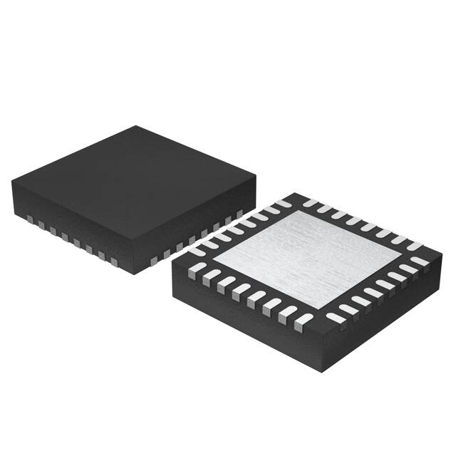


 工商网监
湘ICP备2023018690号
工商网监
湘ICP备2023018690号
