TPS51315
www.ti.com
SLUS881B – MAY 2009 – REVISED AUGUST 2012
10-A STEP-DOWN SYNCHRONOUS SWITCHER WITH INTEGRATED MOSFETs
Check for Samples: TPS51315
FEATURES
APPLICATIONS
•
•
•
•
•
•
1
2
•
•
•
•
•
•
•
•
•
•
•
•
•
•
•
Input Voltage Range: 3 V to 14 V
Output Voltage Range: 0.75 V to 5.5 V
Integrated Power MOSFETs with 10-A
Continuous Current Output
< 5-μA Shutdown Current
D-CAP™ Mode with Fast Transient Response
Programmable Switching Frequency with
External Resistor From 100 kHz to 1 MHz
Selectable Auto-Skip or PWM-Only Operation
< 1% Initial Reference Accuracy
Internal Soft-Start Control
Integrated Boost Diode
Power Good Signal
Adjustable Overcurrent Limit via External
Resistor
OVP/UVP/UVLO Protection
Integrated Selectable Output Discharge
Prebias Output Voltage Start-Up with Disabled
Output Discharge
Thermal Shutdown
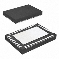
40-Pin QFN Package with Exposed Thermal
Pad
Supports All Ceramic Output Capacitors
Portable Device Application
Notebook Computers
Server and Desktop
DESCRIPTION
The TPS51315 is a D-CAP™ Mode, 10-A,
synchronous step-down converter with integrated
MOSFETs. The combination of D-CAP™ mode and
on-board MOSFETs provides fast transient response
performance with ease of use, less external
component count and small footprint. Externally
adjustable switching frequency allows optimal design
between component size and efficiency tradeoff.
Ceramic output capacitors can be employed by
adding a few extra components. The TPS51315 is
available in the thermally-efficient 40-pin, 5 mm x
7 mm, QFN package and is specified from -40°C to
85°C ambient.
R1
5V
ENSW
R3
R5
R7
29
28
27
26
25
24
23
22
21
V5IN
VBST
N/C
LL
LL
LL
LL
LL
LL
LL
LL
L1
N/C
34
EN_PSV
LL 19
35
TON
LL 18
36
VOUT
C1
LL 17
TPS51315
LL 16
37
VOUT_DS
38
V5FILT
VIN 15
39
VFB
VIN 14
40
PGOOD
VIN 13
GND
PGND
PGND
PGND
PGND
PGND
PGND
VIN
VIN
PGOOD
R6
VOUT
LL 20
33
PGND
C4
30
GND
C3
31
GND
R4
32
TRIP
R2
1
2
3
4
5
6
7
8
9
10
11
12
VIN
3 V to 14 V
C2
UDG-08154
1
2
Please be aware that an important notice concerning availability, standard warranty, and use in critical applications of
Texas Instruments semiconductor products and disclaimers thereto appears at the end of this data sheet.
D-CAP is a trademark of Texas Instruments.
PRODUCTION DATA information is current as of publication date.
Products conform to specifications per the terms of the Texas
Instruments standard warranty. Production processing does not
necessarily include testing of all parameters.
Copyright © 2009–2012, Texas Instruments Incorporated
�TPS51315
SLUS881B – MAY 2009 – REVISED AUGUST 2012
www.ti.com
This integrated circuit can be damaged by ESD. Texas Instruments recommends that all integrated circuits be handled with
appropriate precautions. Failure to observe proper handling and installation procedures can cause damage.
ESD damage can range from subtle performance degradation to complete device failure. Precision integrated circuits may be more
susceptible to damage because very small parametric changes could cause the device not to meet its published specifications.
ORDERING INFORMATION (1)
TJ
ORDERABLE PART
NUMBER
PACKAGE
-40°C to 125°C Plastic QFN (RGF)
(1)
(2)
TPS51315RGFT
TPS51315RGFR
PINS
OUTPUT SUPPLY
40
Tape and Reel
MINIMUM ORDER
QUANTITY
ECO PLAN (2)
250
Green (RoHS and
no Pb/Br)
3000
For most current package and ordering information, see the Package Option Addendum at the end of this document, or see the web site
at www.ti.com.
These devices meet the following planned eco-friendly classification:
Green (RoHS and No Sb/Br): Texas Instruments defines Green to mean Pb-free (RoHS compatible) and free of bromine (Br)- and
antimony (Sb)-based flame retardants. Refer to the Quality and Lead-Free (Pb-Free) Data web site for more information. These devices
have a Cu NiPdAu lead/ball finish.
ABSOLUTE MAXIMUM RATINGS (1)
TPS51315
Input voltage range
Output voltage range
VIN
–0.3 to 20
VBST
–0.3 to 26
VBST (with respect to LL)
–0.3 to 6
EN_PSV, TRIP, V5IN, V5FILT
–0.3 to 6
VOUT, VOUT_DS
–0.3 to 6
TON
–0.3 to 6
LL
–1 to 20
PGOOD
V
–0.3 to 6
PGND
Source/Sink current
V
–0.3 to 0.3
TON
1
VBST
50
mA
Operating free-air temperature, TA
–40 to 85
Storage temperature range, Tstg
–55 to 150
Junction temperature range, TJ
–40 to 125
Lead temperature 1,6 mm (1/16 inch) from case for 10 seconds
(1)
UNIT
°C
300
Stresses beyond those listed under Absolute Maximum Ratings may cause permanent damage to the device. These are stress ratings
only, and functional operation of the device at these or any other conditions beyond those indicated under Recommended Operating
Conditions is not implied. Exposure to absolute-maximum-rated conditions for extended periods may affect device reliability.
RECOMMENDED OPERATING CONDITIONS
MIN
VIN
Input voltage range
VBST (with respect to LL)
EN_PSV, V5IN, V5FILT, VOUT, VOUT_DS
Output voltage range
NOM
MAX
3
14
4.5
5.5
–0.1
5.5
LL
–0.8
15
PGOOD
–0.1
5.5
–40
125
Junction temperature range, TJ
UNIT
V
V
°C
PACKAGE DISSIPATION RATINGS
2
PACKAGE
TA = 25°C
POWER RATING
DERATING FACTOR
ABOVE TA = 25°C
TA = 85°C
POWER RATING
40-Pin Plastic QFN (RGF)
2.85 W
25 mW/°C
1.35 W
Submit Documentation Feedback
Copyright © 2009–2012, Texas Instruments Incorporated
Product Folder Links: TPS51315
�TPS51315
www.ti.com
SLUS881B – MAY 2009 – REVISED AUGUST 2012
ELECTROSTATIC DISCHARGE (ESD) PROTECTION
MIN
Human Body Model (HBM)
TYP
MAX
2000
Charged Device Model (CDM)
500
Submit Documentation Feedback
Copyright © 2009–2012, Texas Instruments Incorporated
Product Folder Links: TPS51315
UNIT
V
3
�TPS51315
SLUS881B – MAY 2009 – REVISED AUGUST 2012
www.ti.com
ELECTRICAL CHARACTERISTICS
over recommended free-air temperature range (unless otherwise noted)
PARAMETER
CONDITIONS
MIN
TYP
MAX
0
1
UNIT
SUPPLY CURRENT
IV5IN
V5IN supply current
V5IN current, TA = 25°C, No Load,
EN_PSV = 5V, VVFB = 0.75 V, VLL = 0.5 V
IV5FILT
V5FILT supply current
V5FILT current, TA = 25°C, No Load,
VEN_PSV = 5 V, VVFB = 0.75 V, LL = 0.5 V
IV5INSDN
V5IN shutdown current
V5IN current, TA = 25°C, No Load,
VEN_PSV = 0 V
IV5FILTSDN
V5FILT shutdown current
V5FILT current, TA = 25°C, No Load,
VEN_PSV = 0 V
μA
400
1.5
μA
0
1
μA
4.5
7.5
μA
5.5
V
VOUT AND VREF VOLTAGES
VOUT
Output voltage
Adjustable output range
VVFB
VFB regulation voltage
VFB voltage
0.75
751
mV
TA = 25°C, bandgap initial accuracy
–0.9%
0.9%
0°C ≤ TA ≤ 85°C
–1.3%
1.3%
–40°C ≤ TA ≤ 85°C
–1.6%
VVFB_TOL
VFB regulation voltage tolerance
IVFB
VFB input current
VVFB = 0.75 V, TA = 25°C
RDischg
VOUT_DS discharge resistance
VEN_PSV = 0 V, VOUT_DS = 0.75 V
1.6%
–0.025
μA
20
Ω
HOUSEKEEPING CLOCK, ON-TIME TIMER, and INTERNAL SOFT START
TONN
Nominal on-time
VIN = 10 V, VOUT = 2.5 V, RT(on) = 250 kΩ
1115
ns
TONF
Fast switch on-time
VIN = 10 V, VOUT = 2.5 V, RT(on) = 100 kΩ
865
ns
TONS
Slow switch on-time
VIN = 10 V, VOUT = 2.5 V, RT(on) = 400 kΩ
1515
ns
TON
(1)
Minimum on-time
VIN = 10 V, VOUT = 0.75 V, RT(on) = 100 kΩ
TOFF(min)
Minimum off-time
TA = 25°C, VVFB = 0.75 V, VLL = –0.1V,
VTRIP = OPEN
385
ns
TSS
Internal soft-start time
TA = 25°C, VEN_PSV > 3 V
1.06
ms
f CLK
Clock frequency
Soft-start, UVP, OVP, PGOOD
(2)
170
200
ns
240
250
260
kHz
0.7
0.8
0.9
V
0.1
1
μA
INTERNAL BST DIODE
VFBST
Forward voltage
VV5IN-VBST, IF = 10 mA, TA = 25°C
IVBSTLK
VBST leakagecurrent
VVBST = 26 V, LL = 20 V, TA = 25°C
PROTECTIONS: OVERCURRENT LIMIT (OCL), UNDERCURRENT LIMIT (UCL)
VOCL(off)
Overcurrent limit comparator offset
(VTRIP-GND– VPGND-LL) voltage
VTRIP-GND = 60 mV
–10
0
10
mV
VUCL(off)
Undercurrent limit comparator offset
(VTRIP-GND– VLL-PGND) voltage
VTRIP-GND = 60 mV, EN_PSV=FLOAT
–9.5
0.5
10.5
mV
VZC(off)
Zero crossing comparator offset
VPGND-LL voltage, V EN_PSV = 3.3V
–9.5
0.5
10.5
mV
10
11
(2)
VRTRIP
Current limit threshold setting range
VTRIP-GND voltage
ITRIP
TRIP source current
VTRIP < 0.3 V, TA = 25°C
TCITRIP
Trip source current temperature
coefficient
TA = 25°C (2)
(1)
(2)
4
, TA = 25°C
30
9
mV
4500
μA
ppm/°C
Design constraint. Ensure actual on-time is greater than the maxiumum value (design RT(on) so that the minimum tolerance is 100 kΩ).
Ensured by design. Not production tested.
Submit Documentation Feedback
Copyright © 2009–2012, Texas Instruments Incorporated
Product Folder Links: TPS51315
�TPS51315
www.ti.com
SLUS881B – MAY 2009 – REVISED AUGUST 2012
ELECTRICAL CHARACTERISTICS (continued)
over recommended free-air temperature range (unless otherwise noted)
PARAMETER
CONDITIONS
MIN
TYP
MAX
UNIT
PG in from lower (PGOOD goes high),
TA = 25°C
92.5%
95%
97.5%
PG Low hysteresis (PGOOD goes low)
–4.5%
–5.5%
–6.5%
PG in from higher (PGOOD goes high),
TA = 25°C
102.5%
105%
107.5%
PG High hysteresis (PGOOD goes low)
4.5%
5.5%
6.5%
2.5
7.5
mA
64
μs
POWERGOOD COMPARATOR
VTH(PG)
Powergood threshold
IPG(max)
Powergood sink current
VPGOOD = 0.5 V
TPGDEL
PGOOD delay
Delay for PGOOD in
UVLO / LOGIC THRESHOLD
VUVLO
VEN_PSV
VEN_PSV
V5FILT UVLO threshold
EN_PSV connection
EN_PSV logic input voltage
Wake up (UVLO out)
3.4
Hysteresis
200
SKIP mode enabled
3.7
3.9
V
300
400
mV
3.3V
PWM-Only mode enabled
FLOAT
EN_PSV low
0.7
1
1.3
V
Hysteresis
130
160
220
mV
EN_PSV float
1.70
1.95
2.25
V
EN_PSV high
2.2
2.5
2.9
V
Hysteresis
100
170
250
mV
110%
115%
120%
65%
70%
PROTECTION: OVERVOLTAGE (OVP) AND UNDERVOLTAGE (UVP)
VOVP
VFB OVP trip threshold
VUVP
VFB UVP trip threshold
TUVPDEL
VFB UVP delay
TUVPEN
Output UVP enable delay
OVP detect
Hysteresis
UVP detect
5%
Hysteresis
75%
10%
32
μs
2
ms
THERMAL SHUTDOWN
TSDN
Thermal SDN threshold
Shutdown temperature (3)
Hysteresis (3)
145
160
175
°C
10
12
14
°C
INTEGRATED MOSFET
RDS(on)upper
RDS(on)lower
(3)
Upper MOSFET RDS(on)
Lower MOSFET RDS(on)
See
(3)
19
mΩ
See
(3)
7
mΩ
Ensured by design. Not production tested.
Submit Documentation Feedback
Copyright © 2009–2012, Texas Instruments Incorporated
Product Folder Links: TPS51315
5
�TPS51315
SLUS881B – MAY 2009 – REVISED AUGUST 2012
www.ti.com
PIN DESCRIPTIONS
PIN
NAME
I/O
DESCRIPTION
NO.
EN_PSV
34
I
Enable/power-save pin. Connect to ground to disable switched-mode power supply (SMPS ). Connect to 3.3
V or 5 V to turn on SMPS and enable skip mode. Float to turn on SMPS but disable skip mode (forced
continuous conduction mode).
I
Signal ground pin.
1
GND
2
4
16
17
18
19
20
21
LL
22
I/O
Source node of the high-side power FET and drain node of the low-side power FET. Connect this pin to
output inductor.
—
No connection inside. Leave open.
I/O
Power GND. Source node of the low-side power FET.
23
24
25
26
27
28
29
NC
33
3
5
6
PGND
7
8
9
10
PGOOD
40
O
Power-good window comparator: open drain output. Pull up to 5-V rail with a pull-up resistor. Current
capability is 7.5 mA.
TON
35
I
On-time / frequency adjustment pin. Connect to LL with proper resistor to program switching frequency.
TRIP
32
I
Overcurrent trip point set input. Connect resistor from this pin to signal ground to set threshold for both
overcurrent and negative overcurrent limit.
V5FILT
38
I
5-V power supply input for all control circuitry except gate drivers. Apply an R-C filter to reject high-frequency
switching noise.
V5IN
31
I
5-V Power supply input for FET gate drivers. Internally connected to VBST by a PN diode. Connect a cpacitor
with a value of 1 μF or greater between this pin and PGND to support instantaneous current for gate drivers.
VBST
30
I
Supply input for high-side FET gate driver (boost terminal). Connect capacitor from this pin to LL-node. An
internal PN diode is connected between V5IN to this pin. Add an external schottky diode if forward drop is
critical to ensure efficient operation.
VFB
39
I
SMPS voltage feedback input. Connect the resistor divider here for adjustable output.
I
Input power source. Drain node of the high-side power FET.
11
12
VIN
13
14
15
VOUT
36
I
Connect to SMPS output. This terminal serves as the output voltage monitor for on-time adjustment.
VOUT_DS
37
O
Prebias start-up and selectable output discharge. It is also the input for the output discharge switch.
6
Submit Documentation Feedback
Copyright © 2009–2012, Texas Instruments Incorporated
Product Folder Links: TPS51315
�TPS51315
www.ti.com
SLUS881B – MAY 2009 – REVISED AUGUST 2012
TRIP
V5IN
VBST
N/C
LL
LL
LL
LL
LL
LL
LL
LL
40-PIN RGY (QFN) PACKAGE
(TOP VIEW)
32
31
30
29
28
27
26
25
24
23
22
21
N/C
33
20
LL
EN_PSV
34
19
LL
TON
35
18
LL
VOUT
36
17
LL
TPS51315
VIN
PGOOD
40
13
VIN
2
3
4
5
6
7
8
9
10
11
12
VIN
1
VIN
14
PGND
39
PGND
VFB
PGND
VIN
PGND
15
PGND
38
PGND
V5FILT
GND
LL
PGND
16
GND
37
GND
VOUT_DS
Submit Documentation Feedback
Copyright © 2009–2012, Texas Instruments Incorporated
Product Folder Links: TPS51315
7
�TPS51315
SLUS881B – MAY 2009 – REVISED AUGUST 2012
www.ti.com
FUNCTIONAL BLOCK DIAGRAM
+5/10%
–30/20%
+
UV
PGOOD
+
Delay
Delay
+
–5/10%
Control Logic
+
OV
+15/10%
0.75 V
SS
VFB
UVP/OVP
Logic
TON
V5IN
+
+
VBST
PWM
VIN
10uA
GND
ISHOT
+ OCP
LL
TRIP
+
LL
PGND
XCON
V5IN
+
ZC/
+ UCP
UCP
Buzz
Logic
PGND
LL
GND
5V
2.9 V
EN_PSV
VOUT_DS
+
+
1V
XPWMonly
Enable
VOUT
On/Off time
Minimum On/Off
Light load
OVP/UVP
Discharge
Fault
Sdn
V5FILT
+
V5OK
THOK
DISCHG
+
160°C/148°C
3.9 V/3.6 V
TPS51315
UDG-09048
8
Submit Documentation Feedback
Copyright © 2009–2012, Texas Instruments Incorporated
Product Folder Links: TPS51315
�TPS51315
www.ti.com
SLUS881B – MAY 2009 – REVISED AUGUST 2012
DETAILED DESCRIPTION
Dual PWM Operations
The primary control loop of the switched-mode power supply (SMPS) functions as an adaptive on-time pulse
width modulation (PWM) controller. It supports a proprietary D-CAP™ mode. D-CAP™ mode uses an internal
compensation circuit and is suitable for a low external component count configuration with an appropriate amount
of equivalent series resistance (ESR) at the output capacitor(s). The output voltage is monitored at a feedback
point voltage.
At the beginning of each cycle, the upper synchronous MOSFET is turned on, or enters the ON state. This
MOSFET is turned off, or enters the OFF state, after an internal one-shot timer expires. This one shot is
determined by the input voltage (VVIN) and the output volage (VOUT) to maintain a relatively constant frequency
over the input voltage range. This is called adaptive on-time control (see PWM Frequency and Adaptive On-Time
Control section). The MOSFET is turned on again when feedback indicates an insufficient output voltage and the
inductor current falls below the overcurrent limit. By repeating the operation in this manner, the controller
regulates the output voltage. The synchronous lower (rectifying) MOSFET is turned on at each OFF state in
order to minimize the conduction losses.
The TPS51315 supports both PWM-Only and Auto-Skip operating modes. When the EN_PSV pin is grounded,
the switcher is disabled. When the EN_PSV pin is connected to a 3.3-V supply or a 5-V supply, Auto-Skip mode
is enabled. The rectifying MOSFET is turned off when the inductor current is zero. This feature enables a
seamless transition to the reduced-frequency operation at light load conditions so that high efficiency is
maintained over a broad range of load currents. When the EN_PSV pin is floated, it is internally pulled up to 1.9
V, and PWM-Only mode is enabled. In this mode, the rectifying MOSFET is not turned off when the inductor
current reaches zero, and so the switching frequency does not change at light load; however the efficiency is
lower in PWM-Only mode than it is in Auto-Skip mode.
The dc output voltage can be set by the external resistor divider as shown in Equation 1.
æ
ö
R
VOUT = ç 1 + UPPER ÷ ´ 0.75 V
è RLOWER ø
(1)
Light Load Conditions
When Auto-Skip mode is enabled, the TPS51315 automatically reduces the switching frequency under light load
conditions to maintain high efficiency.
As the output current decreases from a heavy load condition, the inductor current is also reduced and eventually
its valley falls to zero current, which is the boundary between continuous conduction and discontinuous
conduction modes. The rectifying MOSFET is turned off when zero inductor current is detected. As the load
current continues to decrease, the converter runs in discontinuous conduction mode, taking longer to discharge
the output capacitor toward the reference voltage. The on-time maintains the same as when under a heavy load
condition. Alternatively, when the output current increase from light load to heavy load, switching frequency
increases to the preset value as the inductor current reaches the continuous conduction threshold. The transition
load point to the light load operation IOUT(LL) (that is, the threshold between continuous and discontinuous
conduction mode) can be calculated using Equation 2.
IOUT(LL) =
(VIN - VOUT )´ VOUT
1
´
2´L ´f
VIN
where
•
f is the PWM switching frequency
(2)
Switching frequency versus output current under light load conditions is a function of L, ƒ, VIN and VOUT, but it
decreases almost proportionally to the output current from IOUT(LL) as calculated in Equation 2. For example, it is
approximately 60 kHz at IOUT(LL)/5 when the PWM frequency is 300 kHz.
Submit Documentation Feedback
Copyright © 2009–2012, Texas Instruments Incorporated
Product Folder Links: TPS51315
9
�TPS51315
SLUS881B – MAY 2009 – REVISED AUGUST 2012
www.ti.com
PWM Frequency and Adaptive On Time Control
TPS51315 employs an adaptive on-time control scheme and does not include a dedicated oscillator on the
device. However, the device runs with pseudo-constant frequency by feed-forwarding the input voltage and
output voltage to the on-time, one-shot timer. The on-time control is inversely proportional to the input voltage
and proportional to the output voltage, so that the duty ratio is maintained as VOUT/VIN with the same cycle time,
as shown in Equation 3.
æ (2 / 3)VOUT + 100mV ö
TON = 19 ´ 10-12 ´ RT(on ) ç
÷ + 50ns
VIN
è
ø
where
•
RT(on)x is the external resistor connected from TON to LL
(3)
For the TPS51315, the input voltage is monitored at the LL pin during the ON state. An advantage of switchingnode monitoring is that any loss in the high-side n-channel FET becomes part of the on-time calculation, thereby
making the frequency more stable with load.
Another consideration regarding frequency is jitter. Jitter may have many causes, but the constant on-time DCAP mode scheme has some amount of inherent jitter. Because the output voltage ripple height is in the range
of approximately 20 mV, on the order of a milli-volt of noise on the feedback signal can affect the frequency
between approximately 3% and 10%. This is normal operation and risks only a small amount of influence to the
power supply performance.
Soft-Start
The TPS51315 includes an independent, internal, 1.06-ms, voltage servo soft-start function with overcurrent limit.
When the EN_PSV pin goes high, an internal digita-to-analog converter (DAC) begins ramping up the reference
voltage to the error amplifier. Smooth control of the output voltage is maintained during start-up.
Powergood
The TPS51315 includes a powergood output function. The powergood function is activated after the soft-start
function has completed. If the output voltage comes within ±5% of the target value, internal comparators detect a
powergood state and the powergood signal becomes high after a 64-μs internal delay. If the output voltage rises
above or falls below 10% of the target value, the powergood signal goes low immediately.
Output Discharge Control
The TPS51315 discharges output when EN_PSV is low or when the channel is in either a UVP or OVP fault
condition. The TPS51315 discharges output using an internal 20-Ω MOSFET that is connected to VOUT_DS and
PGND. The current capability of the MOSFET is limited to discharge slowly. An external resistor can be
connected between VOUT_DS and VOUT to program discharge slow rate. In case the discharge function is not
wanted, leave VOUT_DS open.
10
Submit Documentation Feedback
Copyright © 2009–2012, Texas Instruments Incorporated
Product Folder Links: TPS51315
�TPS51315
www.ti.com
SLUS881B – MAY 2009 – REVISED AUGUST 2012
Overcurrent Limit
The TPS51315 has cycle-by-cycle overcurrent limit function. The inductor current is monitored during the OFF
state using the low-side FET RDS(on) which is 7 mΩ (typ). The controller maintains the OFF state and does not
release next ON cycle until the detected current comes down to the overcurrent trip level set by the TRIP
resister. Because of this scheme, RTRIP establishes the valley level of the inductor current. Note that the load
current at the overcurrent threshold, IOCL, is higher than this value calculated in Equation 4.
æ
æI
öö
VTRIP = ç IOCL - ç RIPPLE ÷ ÷ ´ 7 m W
2
è
øø
è
(4)
RTRIP value can be calculated by Equation 5, but cannot exceed 12.1-kΩ to protect the internal FETs from
overloading.
RTRIP =
VTRIP
10 mA
(5)
Undercurrent Limit
The TPS51315 also supports a cycle-by-cycle undercurrent limit in PWM-Only mode. The undercurrent limit is
the negative value of the overcurrent limit. If the output voltage continues to rise, the lower MOSFET is always
on: thus, the inductor current reduces and reverses direction after it reaches zero (in PWM-Only mode). When
there is too much negative current through the inductor, the lower MOSFET is turned off and the current flows to
the VIN pin through the body diode of the upper MOSFET. Because there is less current with which to discharge
the output capacitor, output voltage tends to rise, eventually reaching the overvoltage protection threshold and
shutting down the TPS51315. In order to prevent triggering a false OVP shut down, the lower MOSFET is turned
on 400-ns after it is turned off. If the device reaches an undercurrent threshold again before the output voltage is
discharged to the target level, the lower MOSFET is turned off and the process repeats. This logic is called UCL
Buzz. It ensures maximum allowable discharge capability when the output voltage continues to rise. Alternatively,
if the output voltage is discharged to the target level before the UCL threshold is reached, the lower MOSFET is
turned off, the upper MOSFET is then turned on, and the device resumes normal operation.
Overvoltage Protection
The TPS51315 monitors a resistor-divided feedback voltage to detect overvoltage and undervoltage conditions.
When the feedback voltage becomes greater than 115% of the target value, the upper MOSFET is turned off and
the lower MOSFET is turned on immediately. The output is also discharged by the internal 20-Ω transistor if it is
connected to VOUT_DS.
The, TPS51315 monitors the output voltage directly. If it becomes greater than 5.75 V, TPS51315 turns off the
upper MOSFET driver. In no case should the device operate at more than 6 V, as damage would occur.
Undervoltage Protection
When the feedback voltage becomes lower than 70% of the target value, the undervoltage comparator output
goes high and an internal UVP delay counter begins to increment. After 32 μs, TPS51315 latches off both the
upper and lower MOSFETs and discharges the output with the internal 20-Ω transistor if it is connected to
VOUT_DS. This function is enabled after 2ms from when EN_PSV is brought high, i.e., UVP is disabled during
the start up.
UVLO Protection
The TPS51315 has V5FILT undervoltage lockout (UVLO) protection. When the V5FILT voltage is lower than
UVLO threshold voltage, TPS51315 is shut off. This protection is not latched.
Thermal Shutdown
The TPS51315 includes a die-temperature monitor function. If the temperature exceeds the threshold value
(typically 160°C), TPS51315 shutd off. This protection is not latched. The device recovers once the temperature
has cooled to 148°C.
Submit Documentation Feedback
Copyright © 2009–2012, Texas Instruments Incorporated
Product Folder Links: TPS51315
11
�TPS51315
SLUS881B – MAY 2009 – REVISED AUGUST 2012
www.ti.com
TYPICAL CHARACTERISTICS
At VIN = 12 V, VV5IN = 5 V, RT(on) = 237 kΩ, and TA = 25°C, unless otherwise noted.
V5FILT SHUTDOWN CURRENT
vs
JUNCTION TEMPERATURE
800
8
700
7
IV5FILT_SHDN - Shutdown Current - mA
IV5FILTPWM - Supply Current - mA
PWM SUPPLY CURRENT
vs
JUNCTION TEMPERATURE
600
500
400
300
200
100
0
-50
0
50
100
TJ - Junction Temperature - ºC
4
3
2
1
Figure 2.
TRIP CURRENT
vs
JUNCTION TEMPERATURE
OVP/UVP THRESHOLD
vs
JUNCTION TEMPERATURE
150
130
14
12
10
8
6
0
50
100
TJ - Junction Temperature - º C
150
OVP
120
110
100
90
80
UVP
70
60
50
-50
Figure 3.
12
0
50
100
TJ - Junction Temperature - ºC
Figure 1.
VOVP, VUVP - OVP/UVP Threshold - %
ITRIP - TRIP Source Current - mA
5
0
-50
150
16
4
-50
6
0
50
100
TJ - Junction Temperature - ºC
150
Figure 4.
Submit Documentation Feedback
Copyright © 2009–2012, Texas Instruments Incorporated
Product Folder Links: TPS51315
�TPS51315
www.ti.com
SLUS881B – MAY 2009 – REVISED AUGUST 2012
TYPICAL CHARACTERISTICS (continued)
At VIN = 12 V, VV5IN = 5 V, RT(on) = 237 kΩ, and TA = 25°C, unless otherwise noted.
SWITCHING FREQUENCY
vs
OUTPUT CURRENT
SWITCHING FREQUENCY
vs
OUTPUT CURRENT
450
450
Mode
Auto-Skip
PWM Only
350
Mode
Auto-Skip
PWM Only
400
PWM Only
fSW – Switching Frequency – kHz
fSW – Switching Frequency – kHz
400
300
250
200
150
100
Auto-Skip
50
350
PWM Only
300
250
200
150
100
50
VOUT = 1.05 V
5
0.001
0.01
0.1
1
VOUT = 2.5 V
5
0.001
10
0.01
IOUT – Output Current – A
0.1
1
10
IOUT – Output Current – A
Figure 5.
Figure 6.
OUTPUT VOLTAGE
vs
OUTPUT CURRENT
OUTPUT VOLTAGE
vs
OUTPUT CURRENT
2.54
1.06
2.52
VOUT – Output Voltage – V
VOUT – Output Voltage – V
1.07
1.05
2.50
1.04
2.48
Mode
Auto-Skip
PWM Only
Mode
Auto-Skip
PWM Only
VOUT = 1.05 V
1.03
0
1
2
3
4
5
6
7
8
9
10
2.46
0
1
IOUT – Output Current – A
2
3
4
VOUT = 2.5 V
5
6
7
8
9
10
IOUT – Output Current – A
Figure 7.
Figure 8.
Submit Documentation Feedback
Copyright © 2009–2012, Texas Instruments Incorporated
Product Folder Links: TPS51315
13
�TPS51315
SLUS881B – MAY 2009 – REVISED AUGUST 2012
www.ti.com
TYPICAL CHARACTERISTICS (continued)
At VIN = 12 V, VV5IN = 5 V, RT(on) = 237 kΩ, and TA = 25°C, unless otherwise noted.
OUTPUT VOLTAGE
vs
INPUT VOLTAGE
OUTPUT VOLTAGE
vs
INPUT VOLTAGE
2.54
1.07
2.52
VOUT – Output Voltage – V
VOUT – Output Voltage – V
1.06
2.50
2.48
1.05
2.46
2.44
1.04
ILOAD (A)
ILOAD (A)
2.42
0
10
0
10
VOUT = 1.05 V
2.40
1.03
3
4
5
6
7
8
9
10
11
12
13
3
14
4
5
7
8
9
10
11
12
Figure 9.
Figure 10.
SWITCHING FREQUENCY
vs
INPUT VOLTAGE
MEASURED SWITCHING FREQUENCY
vs
ON-TIME RESISTANCE
13
14
1000
400
PWM Mode
IOUT = 2 A
VOUT (V)
900
fSW – Switching Frequency – kHz
350
fSW – Switching Frequency – kHz
6
VIN – Input Voltage – V
VIN – Input Voltage – V
300
250
200
150
100
VOUT (V)
1.05
2.50
50
1.05
2.50
800
700
600
500
400
300
200
100
0
0
3
4
5
6
7
8
9
10
11
12
13
14
0
100
200
300
400
500
600
700
TON – On-Time Resistance – kW
VIN – Input Voltage – V
Figure 11.
14
VOUT = 2.5 V
Figure 12.
Submit Documentation Feedback
Copyright © 2009–2012, Texas Instruments Incorporated
Product Folder Links: TPS51315
�TPS51315
www.ti.com
SLUS881B – MAY 2009 – REVISED AUGUST 2012
TYPICAL CHARACTERISTICS (continued)
At VIN = 12 V, VV5IN = 5 V, RT(on) = 237 kΩ, and TA = 25°C, unless otherwise noted.
EFFICIENCY
vs
OUTPUT CURRENT
EFFICIENCY
vs
OUTPUT CURRENT
100
100
VOUT = 2.5 V
90
90
80
80
h – Efficiency – %
h – Efficiency – %
VOUT = 1.05 V
70
60
70
60
VIN (V)
VIN (V)
3.3
5.0
12.0
12.6
50
3.3
5.0
12.0
12.6
50
40
40
0
1
2
3
4
5
6
7
8
9
10
0
1
2
3
IOUT – Output Current – A
5
6
7
8
9
10
IOUT – Output Current – A
Figure 13.
Figure 14.
EFFICIENCY
vs
OUTPUT CURRENT
EFFICIENCY
vs
OUTPUT CURRENT
100
100
VIN = 5 V
VIN = 5 V
90
90
80
80
h – Efficiency – %
h – Efficiency – %
4
70
60
VOUT (V)
1.05
1.2
1.8
3.3
50
40
0.001
0.01
0.1
1
70
60
VOUT (V)
50
10
40
0.001
1.1
1.5
2.5
0.01
0.1
1
10
IOUT – Output Current – A
IOUT – Output Current – A
Figure 15.
Figure 16.
Submit Documentation Feedback
Copyright © 2009–2012, Texas Instruments Incorporated
Product Folder Links: TPS51315
15
�TPS51315
SLUS881B – MAY 2009 – REVISED AUGUST 2012
www.ti.com
TYPICAL CHARACTERISTICS (continued)
At VIN = 12 V, VV5IN = 5 V, RT(on) = 237 kΩ, and TA = 25°C, unless otherwise noted.
EFFICIENCY
vs
OUTPUT CURRENT
EFFICIENCY
vs
OUTPUT CURRENT
100
100
VIN = 12 V
90
90
80
80
h – Efficiency – %
h – Efficiency – %
VIN = 12 V
70
60
70
60
VOUT (V)
1.05
1.2
1.8
3.3
50
40
0.001
0.01
0.1
1
VOUT (V)
1.1
1.5
2.5
5.0
50
10
40
0.001
IOUT – Output Current – A
0.01
0.1
1
10
IOUT – Output Current – A
Figure 17. X
X
X
Figure 18. X
X
X
VOUT (500 mV/div)
VOUT (500 mV/div)
LL (10 V/div)
LL (10 V/div)
IOUT (10 A/div)
IOUT (10 A/div)
t – Time – 500 ms/div
t – Time – 500 ms/div
Figure 19. 1.05-V Start-Up Waveforms (Heavy Load)
16
Figure 20. 1.05-V Shut-Down Waveforms (Heavy Load)
Submit Documentation Feedback
Copyright © 2009–2012, Texas Instruments Incorporated
Product Folder Links: TPS51315
�TPS51315
www.ti.com
SLUS881B – MAY 2009 – REVISED AUGUST 2012
TYPICAL CHARACTERISTICS (continued)
At VIN = 12 V, VV5IN = 5 V, RT(on) = 237 kΩ, and TA = 25°C, unless otherwise noted.
VOUT (500 mV/div)
VOUT (500 mV/div)
LL (10 V/div)
LL (10 V/div)
IOUT (10 A/div)
IOUT (10 A/div)
t – Time – 500 ms/div
t – Time – 500 ms/div
Figure 21. 1.05-V Start-Up Waveforms (Light Load)X
X
X
VOUT (20 mV/div)
Figure 22. 1.05-V Shut-Down Waveforms (Light Load)X
X
X
VOUT (20 mV/div)
LL (10 V/div)
LL (10 V/div)
IOUT (10 A/div)
IOUT (10 A/div)
t – Time – 50 ms/div
t – Time – 50 ms/div
Figure 23. 1.05-V Load Step-Up Waveforms
Figure 24. 1.05-V Load Step-Down Waveforms
Submit Documentation Feedback
Copyright © 2009–2012, Texas Instruments Incorporated
Product Folder Links: TPS51315
17
�TPS51315
SLUS881B – MAY 2009 – REVISED AUGUST 2012
www.ti.com
APPLICATION INFORMATION
Loop Compensation and External Parts Selection
Switching Modulator
VIN
R1
Lx
VFB
R2
PWM
+
+
Control
Logic
and
Divider
IL
IC
IO
0.75 V
ESR
RL
Voltage Divider
VC
CO
Output
Capacitor
UDG-09062
Figure 25. Simplified Modulator Block Diagram
The feedback voltage (VVFB) is compared to the internal reference voltage after the divider resistors. The PWM
comparator determines when to turn on the upper MOSFET. The gain and speed of the comparator is high
enough to maintain the voltage level relatively constant at the beginning of each on cycle, or at the end of each
off cycle . The dc output voltage may have line regulation due to ripple amplitude that slightly increases as the
input voltage increases.
For loop stability, the 0 dB frequency, f0, defined in Equation 6 must be lower than 1/4 of the switching frequency.
f0 =
f
1
£ SW
2p ´ ESR ´ COUT
4
(6)
Because f0 is determined solely by the output capacitor characteristics, the loop stability of the D-CAP™ Mode is
determined by capacitor chemistry. For example, specialty polymer capacitors (SP-CAP) have and output
capacitance on the order of several hundred micro-farads and and ESR of approximately 10 mΩ. These values
make f0 on the order of 100 kHz or less and create a stable loop. However, ceramic capacitors have an f0 of
more than 700 kHz, which is not suitable for this operating mode, although the D-CAP™ Mode provides many
advantages such as ease-of-use, minimum external component configuration, and extremely short response
time. These advantages are realized because there is no error amplifier in the loop, so a sufficient feedback
signal is required from an external circuit to reduce the jitter level. The required signal level is approximately 15
mV at the comparing point. This generates output ripple at the output node that can be calculated in Equation 7.
The output capacitor ESR should meet this requirement.
V
ö ´ 15 mV
VRIPPLE = æç OUT
÷
0.75
è
ø
(7)
For applications with all ceramic output capacitors, a few external components need to be added to ensure the
loop stability. Please refer to Figure 29. Since ceramics capacitors have low ESR, feedback ripple in phase with
inductor current is recommended. R-C network across the output inductor can mimic inductor current when RC ≈
L / DCR, the ripple current can be coupled to the feedback through a 1-μF capacitor.
18
Submit Documentation Feedback
Copyright © 2009–2012, Texas Instruments Incorporated
Product Folder Links: TPS51315
�TPS51315
www.ti.com
SLUS881B – MAY 2009 – REVISED AUGUST 2012
External Component Selection
External component selection is a simple process in D-CAP™ Mode.
1. Determine the value of R1 and R2.
The recommended R2 value is 10 kΩ to 100 kΩ. Calculate R1 by using Equation 8.
R1 =
VOUT - 0.75
´ R2
0.75
(8)
2. Choose RT(on)
The switching frequency is usually determined by overall view of the dc-dc converter designer in
consideration of size, efficiency or cost, and mostly dictated by external component constraints such as the
size of inductor and/or the output capacitor. If an extremely low or high duty factor is expected, the minimum
on-time or off-time must also be considered to satisfy the required duty factor. Once the switching frequency
is decided, RT(on) can be determined by Equation 9 and Equation 10.
TON(max ) =
RT(on ) =
1 VOUT
´
f VIN(min )
(9)
(
)
VIN(min )
3 TON(max) - 50ns
´
´
(W )
2
(VOUT + 150mV )
19 ´ 10-12
(10)
3. Choose the inductor.
To begin, choose an inductance value where the ripple current is approximately 1/4 to 1/2 of the maximum
output current.
LIND =
1
IIND(ripple )´f
´
(V
IN(max ) - VOUT
)´ V
OUT
VIN(max )
=
3
IOUT(max ) ´ f
´
(V
IN(max ) - VOUT
)´ V
OUT
VIN(max )
(11)
For applications that require a fast transient response with a minimum of VOUT overshoot, consider a smaller
inductance value than calculated in Equation 11. The cost of a small inductance value is higher steady-state
ripple, larger line regulation, and higher switching loss.
The inductor also needs to have low DCR to achieve good efficiency, as well as enough room above the
peak inductor current before saturation. The peak inductor current can be estimated by Equation 12.
IIND(peak ) =
)
(
VIN(max ) - VOUT ´ VOUT
VTRIP
1
+
´
RDS(on ) 2 ´ L ´ f
VIN(max )
(12)
4. Choose output capacitor(s).
Organic semiconductor capacitor(s) or specialty polymer capacitor(s) are recommended. Determine an ESR
to meet the required ripple voltage. A quick approximation is shown in Equation 13.
ESR =
VOUT ´ 0.015
VOUT
»
´ 60 (mW )
IRIPPLE ´ 0.75 IOUT(max )
(13)
Submit Documentation Feedback
Copyright © 2009–2012, Texas Instruments Incorporated
Product Folder Links: TPS51315
19
�TPS51315
SLUS881B – MAY 2009 – REVISED AUGUST 2012
www.ti.com
5. Choose an RTRIP value.
Select an appropriate RTRIP value with the considerations shown in Equation 14. Maximum RTRIP should be
less than 12.1 kΩ.
RTRIP =
IOUT(max ) ´ 7mW
ITRIP(min )
(14)
6. V5FILT input capacitor.
In order to reject high-frequency noise possibly contained on +5-V supply and V5IN voltages, apply 1-μF of
ceramic capacitor closely at the V5FILT pin with a 10-Ω resistor to create a low-pass filter between +5-V
supply and the pin.
7. Applying the VBST capacitor and VBST diode.
Apply 0.1-μF MLCC between VBST and the LL node as the flying capacitor for internal high-side FET driver.
The TPS51315 has its own on-board boost diode between V5IN and VBST. This diode is a P-N junction
diode and strong enough for most typical applications. However, if efficiency has priority over cost, the
designer may add a Schottky diode externally to improve the gate drive voltage of the high-side FET. A
Schottky diode has a higher leakage current, especially at high temperatures, than a P-N junction diode. A
low-leakage diode should be selected in order to maintain VBST voltage during low-frequency operation in
Auto-Skip mode.
Layout Considerations
Certain concepts must be considered before starting printed curcuit board (PCB) layout work using the
TPS51315.
• Connect the R-C low-pass filter from the 5-V supply to the V5FILT pin. A filter resistance of 10 Ω and a filter
capacitance of 1 μF is recommended. Place the filter capacitor close to the device, within 12 mm (0.5 inches)
if possible.
• Connect the overcurrent setting resistors from TRIP to GND close to the device if possible. The trace from
TRIP to the resistor and from the resistor to GND should avoid coupling to a high-voltage switching node.
• The discharge path (VOUT_DS) should have a dedicated trace to the output capacitor(s); separate from the
output voltage sensing trace, and use a 1,5 mm (60 mils) or wider trace with no loops. Make sure the
feedback current setting resistor (the resistor between VFB to GND) is tied close to the device GND. The
trace from this resistor to the VFB pin should be short and narrow. Place the trace on the component side
and avoid vias between this resistor and the device.
• All sensitive analog traces and components such as VOUT, VFB, GND, EN_PSV, PGOOD, TRIP, V5FILT,
and TON should be placed away from high-voltage switching nodes such as LL or VBST to avoid coupling.
Use internal layer(s) as ground plane(s) and shield the feedback traces from power traces and components.
• Gather the ground terminals of the VIN capacitor(s), VOUT capacitor(s), and the PGND as close as possible.
GND (signal ground) and PGND (power ground) should be connected strongly together near the device. The
PCB trace defined as LL node, which connects to the source of the upper MOSFET, the drain of the lower
MOSFET, and the high-voltage side of the inductor, should be as short and wide as possible.
20
Submit Documentation Feedback
Copyright © 2009–2012, Texas Instruments Incorporated
Product Folder Links: TPS51315
�TPS51315
www.ti.com
SLUS881B – MAY 2009 – REVISED AUGUST 2012
Figure 26. Typical 1.05-V/10-A Application
Submit Documentation Feedback
Copyright © 2009–2012, Texas Instruments Incorporated
Product Folder Links: TPS51315
21
�Submit Documentation Feedback
Product Folder Links: TPS51315
EN_VREG5
VRTC3
EN5
EN3
3
4
5
V3IN
VREG3
VIN
6
7
8
C3
10 mF 1 mF VIN
C4
ENSW
R4
R7
4.5 V to 14 V
PGOOD
R3
R2
R5
R6
TON
VOUT
35
36
1
PGOOD
VFB
39
40
V5FILT
38
VOUT_DS
EN_PSV
34
37
N/C
33
2
3
4
5
TPS51315
6
7
8
9
10
11
LL 16
LL 17
LL 18
LL 19
LL 20
12
C2
VIN 13
VIN 14
VIN 15
21
22
23
24
25
26
27
28
29
30
31
32
R1
GND
1 mF
GND
V5IN
PGND
9
PGND
V5IN 10
V5IN
TRIP
PGND
VREG5
VBST
PGND
GND
LL
N/C
PGND
2
LL
LL
VIN
TPS51103
LL
PGND
VCLK
LL
LL
PGND
LL
GND
LL
22
VIN
1
L1
VIN
UDG-08155
3 V to 14 V
C1
VOUT
TPS51315
SLUS881B – MAY 2009 – REVISED AUGUST 2012
www.ti.com
Figure 27. 1.05-V/10-A Applications with TPS51103
Copyright © 2009–2012, Texas Instruments Incorporated
�TPS51315
www.ti.com
SLUS881B – MAY 2009 – REVISED AUGUST 2012
R1
301 kW
ENSW
R4
20 kW
R3
8.06 kW
D1
32
31
30
29
28
27
26
25
24
23
22
21
TRIP
V5IN
VBST
N/C
LL
LL
LL
LL
LL
LL
LL
LL
R2
12.1 kW
L1
1 mF
LL 20
33
N/C
34
EN_PSV
LL 19
35
TON
LL 18
36
VOUT
LL 17
VOUT
1.8 V
C1
330 mF
LL 16
TPS51315
VOUT
VFB
40
PGOOD
VIN 14
PGND
PGND
VIN
VIN
VIN 13
PGND
R6
100 kW
VIN
12 V
PGND
C5
0.1 mF
39
VIN 15
PGND
R7
27 kW
V5FILT
PGND
C6
0.56 mF
C4 PGOOD
1 mF
38
GND
C3
1 mF
VOUT_DS
PGND
Q1
MMBT3904
37
GND
R6
120 kW
R5
500 W
GND
V5IN
R8
100 W
1
2
3
4
5
6
7
8
9
10
11
12
C2
47 mF
UDG-09046
Figure 28. Typical 1.05-V/10-A Application with Hiccup Operation Mode
Submit Documentation Feedback
Copyright © 2009–2012, Texas Instruments Incorporated
Product Folder Links: TPS51315
23
�TPS51315
3 V to 14 V
VIN
C1
PGOOD
C2
12
11
10
9
PGOOD
5V
C3
R7
R4
C4
R3
ENSW
C6
R2
R6
VFB
39
40
V5FILT
38
VOUT_DS
GND
37
GND
VOUT
PGND
36
8
LL 16
LL 17
LL 18
LL 19
GND
TON
7
TRIP
PGND
35
6
V5IN
TPS51315
PGND
EN_PSV
5
VBST
PGND
34
4
N/C
PGND
N/C
3
LL
PGND
33
2
27
LL
28
1
26
LL
29
VIN 13
25
LL
30
VIN 14
24
LL
31
VIN 15
23
LL
32
LL 20
22
LL
VIN
PGND
R8
L1
21
LL
R1
VIN
C5
UDG-08173
www.ti.com
VOUT
SLUS881B – MAY 2009 – REVISED AUGUST 2012
Figure 29. Typical Applications with All Ceramic Output
24
Submit Documentation Feedback
Copyright © 2009–2012, Texas Instruments Incorporated
Product Folder Links: TPS51315
�TPS51315
www.ti.com
SLUS881B – MAY 2009 – REVISED AUGUST 2012
REVISION HISTORY
Changes from Original (MAY 2009) to Revision A
•
Page
Changed pinout to reflect correct placement of Pin 1 registration mark .............................................................................. 7
Changes from Revision A (MAY 2011) to Revision B
•
Page
Changed ESD HBM rating from "1.5 kV" to "2.0 kV" (typographical error) .......................................................................... 3
Submit Documentation Feedback
Copyright © 2009–2012, Texas Instruments Incorporated
Product Folder Links: TPS51315
25
�PACKAGE OPTION ADDENDUM
www.ti.com
10-Dec-2020
PACKAGING INFORMATION
Orderable Device
Status
(1)
Package Type Package Pins Package
Drawing
Qty
Eco Plan
(2)
Lead finish/
Ball material
MSL Peak Temp
Op Temp (°C)
Device Marking
(3)
(4/5)
(6)
TPS51315RGFR
ACTIVE
VQFN
RGF
40
3000
RoHS & Green
NIPDAU
Level-2-260C-1 YEAR
-40 to 125
TPS
51315
TPS51315RGFT
ACTIVE
VQFN
RGF
40
250
RoHS & Green
NIPDAU
Level-2-260C-1 YEAR
-40 to 125
TPS
51315
(1)
The marketing status values are defined as follows:
ACTIVE: Product device recommended for new designs.
LIFEBUY: TI has announced that the device will be discontinued, and a lifetime-buy period is in effect.
NRND: Not recommended for new designs. Device is in production to support existing customers, but TI does not recommend using this part in a new design.
PREVIEW: Device has been announced but is not in production. Samples may or may not be available.
OBSOLETE: TI has discontinued the production of the device.
(2)
RoHS: TI defines "RoHS" to mean semiconductor products that are compliant with the current EU RoHS requirements for all 10 RoHS substances, including the requirement that RoHS substance
do not exceed 0.1% by weight in homogeneous materials. Where designed to be soldered at high temperatures, "RoHS" products are suitable for use in specified lead-free processes. TI may
reference these types of products as "Pb-Free".
RoHS Exempt: TI defines "RoHS Exempt" to mean products that contain lead but are compliant with EU RoHS pursuant to a specific EU RoHS exemption.
Green: TI defines "Green" to mean the content of Chlorine (Cl) and Bromine (Br) based flame retardants meet JS709B low halogen requirements of