Sample &
Buy
Product
Folder
Support &
Community
Tools &
Software
Technical
Documents
TPS53632
SLUSBW8 – SEPTEMBER 2014
TPS53632 3-2-1 Phase D-CAP+™ Step-Down Driverless Controller
for Low-Voltage Applications with I2C Interface Control
1 Features
3 Description
•
•
The TPS53632 device is a driverless step-down
controller with serial control. Advanced features such
as D-CAP+ architecture provide fast transient
response, lowest output capacitance and high
efficiency. The TPS53632 device supports the
standard I2C Rev 3.0 interface for dynamic control of
the output voltage and current monitor telemetry. It
also has dynamic phase add and drop control and
enters single-phase, discontinuous-current-mode
operation to maximize light-load efficiency.
1
•
•
•
•
•
•
•
•
•
•
•
•
Selectable Phase Count: (3, 2, or 1)
I2C Interface for VID Control and Telemetry with
Eight Device Addresses
D-CAP+™ Control for Fast Transient Response
Dynamic Phase Add and Drop Operation
Switching Frequency: 300 kHz to 1 MHz
Digital Current Monitor
7-Bit, DAC Output Range: 0.50 V to 1.52 V
Optimized Efficiency at Light and Heavy Loads
Accurate, Adjustable Voltage Positioning or Zero
Slope Load-Line
Patented AutoBalance™ Phase Balancing
Selectable, 8-Level Current Limit
2.5-V to 24-V Conversion Voltage Range
Default Boot Voltage: 1.00 V
Small, 4-mm x 4-mm, 32-Pin, VQFN PowerPAD
Package
2 Applications
•
•
Other features include adjustable control of VCORE
slew rate and voltage positioning. The TPS51604
device driver is designed specifically for this
generation of controllers. In addition, the TPS53632
device can be used along with the TI power stage
devices (driver MOSFETs). The TPS53632 device is
packaged in a space saving, thermally enhanced, 32pin VQFN package and is rated to operate at a range
between –10°C and 105°C.
Device Information
PART NUMBER
PACKAGE
BODY SIZE
TPS53632
VQFN
4 mm × 4 mm
High-Current, Low-Voltage Applications
Core Power for Microservers, Custom
Microcontrollers, ASICs
Simplified Schematic
TPS53632
PWM1
Power Stage
Driver
Power
Block
Power Stage
Control BUS
PWM2
Driver
Power
Block
Power Stage
PWM3
SKIP
Driver
Power
Block
VO
1
An IMPORTANT NOTICE at the end of this data sheet addresses availability, warranty, changes, use in safety-critical applications,
intellectual property matters and other important disclaimers. PRODUCTION DATA.
�TPS53632
SLUSBW8 – SEPTEMBER 2014
www.ti.com
Table of Contents
1
2
3
4
5
6
Features ..................................................................
Applications ...........................................................
Description .............................................................
Revision History.....................................................
Pin Configuration and Functions .........................
Specifications.........................................................
6.1
6.2
6.3
6.4
6.5
6.6
6.7
6.8
6.9
7
7.2
7.3
7.4
7.5
7.6
1
1
1
2
3
4
8
Functional Block Diagram .......................................
Feature Description.................................................
Device Functional Modes........................................
Configuration and Programming .............................
Register Maps ........................................................
12
12
20
20
21
Applications and Implementation ...................... 23
8.1 Application Information............................................ 23
8.2 Typical Application .................................................. 23
Absolute Maximum Ratings ...................................... 4
Handling Ratings....................................................... 4
Recommended Operating Conditions....................... 5
Thermal Information .................................................. 5
Electrical Characteristics........................................... 6
Timing Requirements ................................................ 8
Switching Characteristics .......................................... 8
Typical Characteristics (2-Phase Operation) ............ 9
Typical Characteristics (3-Phase Operation) .......... 10
9 Power Supply Recommendations...................... 31
10 Layout................................................................... 32
10.1 Layout Guidelines ................................................. 32
10.2 Layout Example .................................................... 35
11 Device and Documentation Support ................. 35
11.1 Trademarks ........................................................... 35
11.2 Electrostatic Discharge Caution ............................ 35
11.3 Glossary ................................................................ 35
Detailed Description ............................................ 11
12 Mechanical, Packaging, and Orderable
Information ........................................................... 35
7.1 Overview ................................................................. 11
4 Revision History
NOTE: Page numbers for previous revisions may differ from page numbers in the current version.
2
DATE
REVISION
NOTES
September 2014
*
Initial release.
Submit Documentation Feedback
Copyright © 2014, Texas Instruments Incorporated
Product Folder Links: TPS53632
�TPS53632
www.ti.com
SLUSBW8 – SEPTEMBER 2014
5 Pin Configuration and Functions
25 DROOP
26 COMP
27 V REF
28 V 5A
29 G ND
31 S CL
30 NC
32 NC
RSM (QFN) PACKAGE
32 PINS
(TOP VIEW)
SDA
1
24 VFB
VDD
2
23 GFB
PGOOD
3
22 CSN3
PWM 3
4
21 CSP3
TPS53632
18 CSN1
EN
8
17 CSP1
PU
V IN 16
7
SL EWA 15
SKIP
VINTF 14
19 CSN2
IMON 13
6
OCP-I 12
PWM 1
RAMP 11
20 CSP2
FREQ -P 10
5
9
PWM 2
Pin Functions
PIN
NAME
NO.
COMP
26
CSP1
17
CSP2
20
CSP3
21
CSN1
18
CSN2
19
CSN3
22
DROOP
I/O
DESCRIPTION
I
Error amplifier summing node. Resistors between the VREF pin and the COMP pin (RCOMP) and
between the COMP pin and the DROOP pin (RDROOP) set the droop gain.
I
Positive current sense inputs. Connect to the most positive node of current sense resistor or inductor
DCR sense network. Tie CSP3, CSP2 or CSP1 (in that order) to a 3.3-V supply to disable the phase.
I
Negative current sense inputs. Connect to the most negative node of current sense resistor or
inductor DCR sense network. CSN1 has a secondary OVP comparator and includes the soft-stop,
pull-down transistor.
25
O
Error amplifier output. A resistor pair between this pin and the VREF pin and between the COMP pin
and this pin sets the droop gain. ADROOP = 1 + RDROOP / RCOMP.
EN
8
I
Enable. 100-ns de-bounce. Regulator enters low-power mode, but retains start-up settings when
brought low.
FREQ-P
10
I
A resistor between this pin and GND sets the per-phase switching frequency. Add a resistor to VREF
to disable dynamic phase add and drop operation.
GFB
23
I
Voltage sense return. Tie to GND on PCB with a 10-Ω resistor to provide feedback when the
microprocessor is not populated.
GND
29
–
Analog circuit reference. Tie this pin to a quiet point on the ground plane.
IMON
13
O
Analog current monitor output. VIMON = ΣVISENSE × (1 + RIMON/ROCP).
OCP-I
12
I/O
Voltage divider to IMON. Resistor ratio sets the IMON gain (see IMON pin). A resistor between this
pin and GND (ROCP) selects 1 of 8 OCP levels (per phase, latched at start-up).
PU
9
I
Pull-up to VREF through 10-kΩ resistor.
PGOOD
3
O
Power good output. Open-drain.
PWM1
4
PWM2
5
O
PWM controls for the external driver; 5-V logic level. Controller forces signal to the tri-state level
when needed.
–
No connect.
PWM3
NC
6
30
32
Submit Documentation Feedback
Copyright © 2014, Texas Instruments Incorporated
Product Folder Links: TPS53632
3
�TPS53632
SLUSBW8 – SEPTEMBER 2014
www.ti.com
Pin Functions (continued)
PIN
I/O
DESCRIPTION
NAME
NO.
RAMP
11
I
Voltage divider to VREF. A resistor to GND sets the ramp setting voltage. The RAMP setting can be
used to override the factory ramp setting.
SCL
31
I
Serial digital clock line.
SDA
1
I/O
Serial digital I/O line.
SKIP
7
O
When high, the driver enters FCCM mode; otherwise, the driver is in DCM mode. Driving the tri-state
level on this pin puts the drivers into a low power sleep mode.
SLEWA
15
I
The voltage sets the 3 LSBs of the I2C address. The resistance to GND selects 1 of 8 slew rates. The
start-up slew rate (EN transitions high) is SLEWRATE/2. The ADDRESS and SLEWRATE values are
latched at start-up.
VINTF
14
I
Input voltage to interface logic. Voltage level can be between 1.62 V and 3.5 V.
V5A
28
I
5-V power input for analog circuits; connect through resistor to 5-V plane and bypass to GND with
ceramic capacitor with a value of at least 1 µF.
VIN
16
I
10-kΩ resistor to the VIN pin provides input voltage information to the on-time circuits for both
converters.
VDD
2
I
3.3-V digital power input. Bypass this pin to GND with a capacitor with a value of at least 1 µF.
VFB
24
I
Voltage sense line. Tie directly to VOUT sense point of processor. Tie to VOUT on PCB with a 10-Ω
resistor to provide feedback when the microprocessor is not populated. The resistance between VFB
and GFB is > 1 MΩ
27
O
1.7-V, 500-µA reference. Bypass to GND with a 0.22-µF ceramic capacitor.
GND
–
Thermal pad Tie to the ground plane with multiple vias.
VREF
PAD
6 Specifications
6.1 Absolute Maximum Ratings
over operating free-air temperature range (unless otherwise noted)
Input voltage
Output voltage
(1)
MIN
MAX
PWM3, PWM2, PWM1, SKIP, V5A
–0.3
6.0
VIN
–0.3
30.0
COMP, CSP1, CSP2, CSP3, CSN1, CSN2, CSN3, DROOP, EN,
FREQ-P, IMON, OCP-I, O-USR, RAMP, SCL, SDA, SLEWA, VDD,
VFB, VINTF, VREF
–0.3
3.6
GFB
–0.2
0.2
PGOOD
–0.3
3.6
V
–40
150
°C
Operating junction temperature, TJ
(1)
UNIT
V
Stresses beyond those listed under Absolute Maximum Ratings may cause permanent damage to the device. These are stress ratings
only, which do not imply functional operation of the device at these or any other conditions beyond those indicated under Recommended
Operating Conditions. Exposure to absolute-maximum-rated conditions for extended periods may affect device reliability.
6.2 Handling Ratings
Tstg
Storage temperature
V(ESD) (1)
(1)
(2)
4
Human body model (HBM) ESD stress voltage (1)
Charged device model (CDM) ESD stress voltage (2)
MIN
MAX
–55
150
UNIT
°C
–2
2
kV
–750
750
V
JEDEC document JEP155 states that 500-V HBM allows safe manufacturing with a standard ESD control process.
JEDEC document JEP157 states that 250-V CDM allows safe manufacturing with a standard ESD control process.
Submit Documentation Feedback
Copyright © 2014, Texas Instruments Incorporated
Product Folder Links: TPS53632
�TPS53632
www.ti.com
SLUSBW8 – SEPTEMBER 2014
6.3 Recommended Operating Conditions
over operating free-air temperature range (unless otherwise noted)
VI
Input voltage
VO
Output voltage
TA
Operating ambient temperature
MIN
MAX
CSN1, CSN2, CSN3, CSP1, CSP2, CSP3,
IMON, , OCP-I, O-USR, RAMP, SCL, SDA, VDD,
VFB, VINTF, VREF
UNIT
–0.1
3.5
VIN
–0.1
28
COMP, DROOP, EN, FREQ-P, PWM3, PWM2,
PWM1, SKIP, SLEWA, V5A
–0.1
5.5
GFB
–0.1
0.1
PGOOD
–0.1
3.5
V
–10
105
°C
V
6.4 Thermal Information
TPS53632
THERMAL METRIC (1)
RSM (VQFN)
UNITS
32 PINS
θJA
Junction-to-ambient thermal resistance (2)
37.2
θJCtop
Junction-to-case (top) thermal resistance (3)
31.9
θJB
Junction-to-board thermal resistance (4)
8.1
ψJT
Junction-to-top characterization parameter (5)
0.4
ψJB
Junction-to-board characterization parameter (6)
7.9
θJCbot
Junction-to-case (bottom) thermal resistance (7)
2.2
(1)
(2)
(3)
(4)
(5)
(6)
(7)
°C/W
For more information about traditional and new thermal metrics, see the IC Package Thermal Metrics application report, SPRA953.
The junction-to-ambient thermal resistance under natural convection is obtained in a simulation on a JEDEC-standard, high-K board, as
specified in JESD51-7, in an environment described in JESD51-2a.
The junction-to-case (top) thermal resistance is obtained by simulating a cold plate test on the package top. No specific JEDECstandard test exists, but a close description can be found in the ANSI SEMI standard G30-88.
The junction-to-board thermal resistance is obtained by simulating in an environment with a ring cold plate fixture to control the PCB
temperature, as described in JESD51-8.
The junction-to-top characterization parameter, ψJT, estimates the junction temperature of a device in a real system and is extracted
from the simulation data for obtaining θJA, using a procedure described in JESD51-2a (sections 6 and 7).
The junction-to-board characterization parameter, ψJB, estimates the junction temperature of a device in a real system and is extracted
from the simulation data for obtaining θJA , using a procedure described in JESD51-2a (sections 6 and 7).
The junction-to-case (bottom) thermal resistance is obtained by simulating a cold plate test on the exposed (power) pad. No specific
JEDEC standard test exists, but a close description can be found in the ANSI SEMI standard G30-88.
Spacer
Submit Documentation Feedback
Copyright © 2014, Texas Instruments Incorporated
Product Folder Links: TPS53632
5
�TPS53632
SLUSBW8 – SEPTEMBER 2014
www.ti.com
6.5 Electrical Characteristics
over recommended free-air temperature range, 4.5 V ≤ VV5A ≤ 5.5 V, 3.0 V ≤ VVDD ≤ 3.6 V, VGFB = GND, VVFB = VCORE (unless
otherwise noted).
PARAMETER
CONDITIONS
MIN
TYP
MAX
UNIT
POWER SUPPLY: CURRENTS, UVLO AND POWER-ON-RESET
IV5-3P
V5A supply current
3-phase operation, VDAC < VVFB < (VDAC + 100 mV), EN = ‘HI’
3.6
6.0
IVDD-3P
VDD supply current
3-phase operation, VDAC < VVFB < (VDAC + 100 mV), EN = ‘HI’,
digital buses idle
0.2
0.8
IV5-1P
V5A supply current
1-phase operation, VDAC < VVFB < (VDAC + 100 mV) , EN = ‘HI’
3.5
6.0
IVDD-1P
VDD supply current
1-phase operation, VDAC < VVFB < (VDAC + 100 mV), EN = ‘HI’,
digital buses idle
0.2
0.8
IV5STBY
V5A standby current
EN = ‘LO’
125
200
IVDDSTBY
VDD standby current
EN = ‘LO’
23
40
IVDD-1P8
VINTF supply current
All conditions, digital buses idle
1.7
5.0
VUVLOH
V5A UVLO ‘OK’ threshold
VVFB < 200 mV, Ramp up, VVDD > 3 V, EN = ’HI’, switching
begins.
4.2
4.4
4.52
VUVLOL
V5A UVLO fault threshold
Ramp down, EN = ’HI’, VVDD > 3 V, VVFB = 100 mV, restart if 5V falls below VPOR then rises > VUVLOH, or EN is toggled w/ VV5A
> VUVLOH
4.00
4.2
4.35
VPOR
V5A fault latch reset threshold
Ramp down, EN = ‘HI’, VVDD > 3 V. Can restart if 5-V rises to
VUVLOH and no other faults present.
1.2
1.9
2.5
V3UVLOH
VDD UVLO ‘OK’ threshold
VVFB < 200 mV. Ramp up, VV5A > 4.5 V, EN = ’HI’, Switching
begins.
2.5
2.8
3.0
V3UVLOL
Fault threshold
Ramp down, EN = ’HI’, V5A > 4.5V, VFB = 100 mV, restart if 5V dips below VPOR then rises > VUVLOH or EN is toggled with 5 V
> VUVLOH
2.4
2.6
2.8
VPOR
VDD fault latch
Ramp down, EN = ‘HI’, VV5A > 4.5 V, can restart if 5-V supply
rises to VUVLOH and no other faults present.
1.2
1.9
2.5
VINTFUVLOH
VINTF UVLO OK
Ramp up, EN = ’HI’, VV5A > 4.5 V, VVFB = 100 mV
1.4
1.5
1.6
VINTFUVLOL
VINTF UVLO falling
Ramp down, EN = ’HI’, VV5A > 4.5 V, VVFB = 100 mV
1.3
1.4
1.5
mA
µA
V
REFERENCES: DAC, VREF, VFB DISCHARGE
VVIDSTP
VID step size
Change VID0 HI to LO to HI
VDAC1
VFB tolerance
No load active, 1.36 V ≤ VVFB ≤ 1.52 V, IOUT = 0 A
–9
9
No load medium, 1.0 V ≤ VVFB ≤ 1.35 V, IOUT = 0 A
–8
8
VDAC2
VFB tolerance
VVREF
VREF output
VREF output 4.5 V ≤ VV5A ≤ 5.5 V, IVREF = 0 A
VVREFSRC
VREF output source
0 A ≤ IREF ≤ 500 µA, HP-2
VVREFSNK
VREF output sink
–500 A ≤ IREF ≤ 0 A, HP-2
VVBOOT
Internal VFB initial boot voltage
Initial DAC boot voltage
No load medium, 0.5 V ≤ VVFB ≤ 0.99 V, IOUT = 0 A
10
-7
7
1.66
1.700
–4
-3
0.99
mV
1.74
3
4
1.00
1.01
V
mV
V
RAMP SETTINGS
VRAMP
Compensation ramp
RRAMP = 30 kΩ
60
RRAMP = 56 kΩ
120
RRAMP = 100 kΩ
160
RRAMP ≥ 150 kΩ
40
mV
VOLTAGE SENSE: VFB AND GFB
RVFB
VFB/GFB Input resistance
Not in fault, disable or UVLO, VVFB = VDAC = 1.5 V,
VGFB = 0 V, measure from VFB to GFB
VDELGND
GFB Differential
GND to GFB
1
MΩ
±100
mV
CURRENT MONITOR
VALADC
LRIMON
6
IMON ADC output
IMON linear range
∑∆CS = 0 mV, AIMON = 3.867
00h
∑∆CS = 1.5 mV, AIMON = 3.867
19h
∑∆CS = 7.5 mV, AIMON = 3.867
80h
∑∆CS = 15 mV, AIMON = 3.867
FFh
Each phase, CSPx – CSNx
Submit Documentation Feedback
50
mV
Copyright © 2014, Texas Instruments Incorporated
Product Folder Links: TPS53632
�TPS53632
www.ti.com
SLUSBW8 – SEPTEMBER 2014
Electrical Characteristics (continued)
over recommended free-air temperature range, 4.5 V ≤ VV5A ≤ 5.5 V, 3.0 V ≤ VVDD ≤ 3.6 V, VGFB = GND, VVFB = VCORE (unless
otherwise noted).
PARAMETER
CONDITIONS
MIN
TYP
MAX
UNIT
CURRENT SENSE: OVER CURRENT PROTECTION, PHASE ADD AND DROP, AND PHASE BALANCE
VOCPP
OCP voltage (valley current
limit)
ROCP-I = 20 kΩ
3.7
7.6
11.4
ROCP-I = 24 kΩ
6.6
10.5
14.1
ROCP-I = 30 kΩ
10.6
14.5
18.0
ROCP-I = 39 kΩ
15.4
19.5
23.0
ROCP-I = 56 kΩ
21.3
25.4
29.0
ROCP-I = 75 kΩ
28.4
32.5
36.2
ROCP-I = 100 kΩ
36.3
40.5
44.0
ROCP-I = 150 kΩ
45.0
49.3
53.0
IAD23
Phase add
Valley current, % of OCP value, mode changes from 2-phase
CCM to 3-phase CCM
IAD12
Phase add
Valley current, % of OCP value, mode changes from 1-phase
DCM to 2-phase CCM
10%
IAD32
Phase drop
Valley current, % of OCP value, mode changes from 3-phase
CCM to 2-phase CCM
15%
IAD21
Phase drop
Valley current, % of OCP value, mode changes from 2-phase
CCM to 1-phase DCM
7%
ICS
CS pin input bias current
CSPx and CSNx
AV-EA
Error amplifier total voltage
gain (1)
VFB to DROOP
IEA_SR
Error amplifier source current
IDROOP, VVFB = VDAC + 50 mV, RCOMP = 1 kΩ
1
IEA_SK
Error amplifier sink current
IDROOP, VVFB = VDAC – 50mV, RCOMP = 1 kΩ
–1
ACSINT
Internal current sense gain
Gain from CSPx – CSNx to PWM comparator, RSKIP = Open
RSFTSTP
Soft-stop transistor resistance
Connected to CSN1
VDP_OFF
Voltage to disable dynamic
phase add/drop
Voltage at FREQ-P at start-up
VDP_ON
Voltage to enable dynamic
phase add/drop
Voltage at FREQ-P at start-up
VDP_HYS
Hysteresis voltage of phase
add/drop circuit
Voltage at FREQ-P at start-up
RVIN
VIN resistance
–500
25%
0.2
500
80
5.8
mV
nA
dB
mA
6.0
6.2
V/V
100
200
Ω
0.70
V
0.40
80
EN = HI
350
EN = LOW or STBY
mV
600
10
kΩ
MΩ
PROTECTION: OVP, UVP, PGOOD AND THERMAL SHUTDOWN
VOVPH
Fixed OVP voltage
VCSN1 > VOVPH for 1 µs
1.60
VPGDH
PGOOD high threshold
Measured at the VFB pin w/r/t VID code, device latches OFF
190
1.70
1.80
245
VPGDL
PGOOD low threshold
Measured at the VFB pin w/r/t VID code, device latches OFF
-348
-280
V
mV
PWM AND SKIP OUTPUTS: I/O VOLTAGE AND CURRENT
VP-S_L
PWMx/SKIP - Low
PWMILOAD = ± 1 mA, SKIPILOAD = ± 100 µA
VP-S_H
PWMx/SKIP - High
PWMILOAD = ± 1 mA, SKIPILOAD = ± 100 µA
4.2
VPW-SKLK
PWMx tri-state
PWMILOAD = ± 100 µA
1.6
0.15
0.3
1.7
1.8
V
LOGIC INTERFACE: VOLTAGE AND CURRENT
RVRTTL
RVRPG
Pull-down resistance
IVRTTLK
Logic leakage current
VIL
Low-level Input voltage
VIH
High-level Input voltage
IENH
I/O leakage, EN
(1)
VSDA = 0.31
4
VPGOOD= 0.31
VSCL= 1.8 V, VSDA = 1.8 V, VPGOOD = 3.3 V
SCL, SDA; VVINTF = 1.8 V
Leakage current , VEN = 1.8 V
15
36
-2
0.2
50
2
0.6
1.2
24
40
Ω
µA
V
µA
Specified by design. Not propduction tested.
Submit Documentation Feedback
Copyright © 2014, Texas Instruments Incorporated
Product Folder Links: TPS53632
7
�TPS53632
SLUSBW8 – SEPTEMBER 2014
www.ti.com
6.6 Timing Requirements
The TPS53632 requires the ENABLE signal on Pin 8 to go from low to high only after the V5A (5V), the VDD
(3.3V) and the VIN rails have gone high.
6.7 Switching Characteristics
over operating free-air temperature range (unless otherwise noted)
PARAMETER
TEST CONDITIONS
MIN
tOFF(min)
Controller minimum OFF
time
Fixed value
20
tON(min)
Controller minimum ON
time
RCF = 150 kΩ, VVIN = 20 V, VVFB = 0 V
20
TYP
MAX
UNIT
ns
TIMERS: SLEW RATE, ADDR, SLEEP EXIT, ON TIME AND I/O TIMING
tSTART-CB
Cold boot time (1)
VBOOT > 0V , EN = high, CREF = 0.33 µF
1.2
ms
tSTBY-E
Standby exit time (2)
VVID = 1.28 V, RSLEW = 39 kΩ
250
µs
Slew rate setting for VID
change
SLSET
SLSTART (3)
Slew rate setting for startup
ADDR
Address setting 3 LSB of
I2C address
RSLEW = 20 kΩ
6
RSLEW = 24 kΩ
12
RSLEW = 30 kΩ
18
RSLEW = 39 kΩ
24
RSLEW = 56 kΩ
30
EN goes high, RSLEW = 39 kΩ
12
mV/µs
mV/µs
VSLEWA ≤ 0.30 V (Addr = 100 0xxx)
000b
0.75 V ≤ VSLEWA ≤ 0.85 V
011b
1.15 V ≤ VSLEWA ≤ 1.25 V
101b
tPGDDGLTO
PGOOD deglitch time
(over) (4)
1
tPGDDGLTU
PGOOD deglitch time
(under) (5)
31
tON
On time
µs
RCF = 20 kΩ
295
RCF = 24 kΩ, VVIN = 12 V, VVFB = 1 V (400 kHz)
230
RCF = 39 kΩ, VVIN = 12 V, VVFB = 1 V (600 kHz)
164
RCF = 75 kΩ, VVIN = 12 V, VVFB = 1 V (800 kHz)
140
RCF = 150 kΩ, VVIN = 12 V, VVFB = 1 V (1 MHz)
128
ns
PWM AND SKIP OUTPUTS
tP-S_H-L (3)
PWMx/SKIP H-L transition
time
10% to 90%, both edges
7
20
tP-S_TRI (3)
PWMx tri-state transition
10% or 90% to tri-state level, both edges
5
20
250
275
ns
PROTECTION: OVP, UVP, PGOOD AND THERMAL SHUTDOWN
tPG2
(1)
(2)
(3)
(4)
(5)
8
PGOOD low after enable
goes low
Low state time after EN goes low.
225
µs
Cold boot time is defined as the time from UVLO detection to VOUT ramp.
Standby exit time is defined as the time from EN assertion until PGOOD goes high
Specified by design. Not production tested.
PGOOD deglitch time (over) is defined as the time from when the VFB pin rises above the 250-mV VDAC boundary to when the PGOOD
pin goes low.
PGOOD deglitch time (under) is defined as the time from when the VFB pin falls below the –300-mV VDAC boundary to when the
PGOOD pin goes low.
Submit Documentation Feedback
Copyright © 2014, Texas Instruments Incorporated
Product Folder Links: TPS53632
�TPS53632
www.ti.com
SLUSBW8 – SEPTEMBER 2014
6.8 Typical Characteristics (2-Phase Operation)
VIN = 12 V
VOUT = 1 V
Load = 1 A
VIN = 12 V
Figure 1. Startup
VIN = 12 V
VOUT = 1 V
VOUT = 1 V
Load = 10 A
Figure 2. Switching Waveform
Load = 4 A to 20 A
I2C command
Δ VOUT, 1.0 V to 1.1 V
Figure 3. Load Transient
VIN = 12 V
VOUT = 1 V
Figure 4. Output Voltage Change
Load = 1 A to 25 A
VIN = 12 V
Figure 5. Auto Phase Add
VOUT = 1 V
Load = 25 A to 1 A
Figure 6. Auto Phase Drop
Submit Documentation Feedback
Copyright © 2014, Texas Instruments Incorporated
Product Folder Links: TPS53632
9
�TPS53632
SLUSBW8 – SEPTEMBER 2014
www.ti.com
6.9 Typical Characteristics (3-Phase Operation)
VIN = 12 V
VOUT = 1 V
Load = 1 A
VIN = 12 V
Figure 7. Startup
VIN = 12 V
VOUT = 1 V
VOUT = 1 V
Load = 9 A to 35 A
I2C command
Δ VOUT, 1.0 V to 1.1 V
Figure 10. Output Voltage Change
Load = 1 A to 31 A
VIN = 12 V
Figure 11. Auto Phase Add
10
Load = 30 A
Figure 8. Switching Waveform
Figure 9. Load Transient
VIN = 12 V
VOUT = 1 V
VOUT = 1 V
Load = 31 A to 1 A
Figure 12. Auto Phase Drop
Submit Documentation Feedback
Copyright © 2014, Texas Instruments Incorporated
Product Folder Links: TPS53632
�TPS53632
www.ti.com
SLUSBW8 – SEPTEMBER 2014
7 Detailed Description
7.1 Overview
The TPS53632 device is a DCAP+ mode adaptive on-time controller. The DAC outputs a reference in
accordance with the 8-bit VID code as defined in Table 2. This DAC sets the output voltage.
In adaptive on-time converters, the controller varies the on-time as a function of input and output voltage to
maintain a nearly constant frequency during steady-state conditions. With conventional voltage-mode constant
on-time converters, each cycle begins when the output voltage crosses to a fixed reference level. However, in
the TPS53632 device, the cycle begins when the current feedback reaches an error voltage level which
corresponds to the amplified difference between the DAC voltage and the feedback output voltage. In the case of
two-phase or three-phase operation, the device sums the current feedback from all the phases at the output of
the internal current-sense amplifiers.
This approach has two advantages:
• The amplifier DC gain sets an accurate linear load-line slope, which is required for CPU core applications.
• The device filters the error voltage input to the PWM comparator to improve the noise performance.
In addition, a value representing the difference between the DAC-to-output voltage and the current feedback,
goes through an integrator to give an approximately linear load-line slope even at light loads where the inductor
current is in discontinuous conduction mode (DCM).
During a steady-state condition, the phases of the TPS53632 switch 180° phase-displacement for two-phase
mode and 120° phase-displacement for three-phase mode. The phase displacement is maintained both by the
architecture (which does not allow the high-side gate drive outputs of more than one phase to be ON in any
condition except transients) and the current ripple (which forces the pulses to be spaced equally). The controller
forces current-sharing by adjusting the ON-time of each phase. Current balancing requires no user intervention,
compensation, or extra components.
Submit Documentation Feedback
Copyright © 2014, Texas Instruments Incorporated
Product Folder Links: TPS53632
11
�TPS53632
SLUSBW8 – SEPTEMBER 2014
www.ti.com
7.2 Functional Block Diagram
COMP
DROOP
VDD
Ramp
Comparator
+
GFB
+
+
IAMP
Error
Amplifier
Integrator
+
IS1
VBAT
PWM1
PWM2
PWM3
On-Time PWM1
1
PWM1
On-Time PWM2
2
PWM2
On-Time PWM3
3
PWM3
CLK1
Voltage
Amplifier
DAC
CSP1
GND
VREF
Clamp
Differential
Amplifier
VFB
V5A
+
+
CLK
BLANK
Phase
Manager
CLK2
CLK3
ISUM
CSN1
ISUM
CSP2
+
IAMP
DROOP
IS2
CSN2
+
CSP3
+
IAMP
Current
Sharing
Circuitry
+
6
ADDR
ILIM
OCP
PS0
PS1
PS2
PS3
VD
ISUM
IS1
IS2
IS3
CSN3
EN
DAC
PGOOD
DAC
SCL
SVID
Interface
SKIP
FREQ-P
OCP-I
O-USR
VINTF
B-RAMP
IMON
CPU
Logic, Protection,
and Status Circuitry
FSEL
VREF
SLEWA
OSR
ISHARE
+
IS3
SDA
USR
OSR/USR
7.3 Feature Description
7.3.1 Current Sensing
The TPS53632 device provides independent channels of current feedback for every phase. These independent
channels increase the system accuracy and reduce the dependence of circuit performance on layout compared
to an externally summed architecture. The design can use inductor DCR sensing to yield the best efficiency or
resistor current sensing to yield the most accuracy across wide temperature ranges. DCR sensing can be
optimized by using a NTC thermistor to reduce the variation of current sense with temperature.
The pins CSP1, CSN1, CSP2, CSN2 and CSP3, CSN3 are the current sensing pins.
7.3.2
Load Transients
When the load increases suddenly, the output voltage immediately drops. This voltage drop is reflected as a
rising voltage on the DROOP pin. This rising voltage forces the PWM to pulse sooner and more frequently which
causes the inductor current to rapidly increase. As the inductor current reaches the new load current, a steadystate operating condition is reached and the PWM switching resumes the steady-state frequency. Similarly, when
the load releases suddenly, the output voltage rises. This rise is reflected as a falling voltage on the COMP pin.
This rising voltage forces a delay in the PWM pulses until the inductor current reaches the new load current,
when the switching resumes and steady-state switching continues.
7.3.3 AutoBalance™ Current Sharing
The basic mechanism for current sharing is to sense the average phase current, then adjust the pulse width of
each phase to equalize the current in each phase.
12
Submit Documentation Feedback
Copyright © 2014, Texas Instruments Incorporated
Product Folder Links: TPS53632
�TPS53632
www.ti.com
SLUSBW8 – SEPTEMBER 2014
Feature Description (continued)
The PWM comparator (not shown) starts a pulse when the feedback voltage equals the reference voltage. The
VIN voltage charges the Ct(on) capacitor through the resistor Rt(on). The pulse is terminated when the voltage at
capacitor Ct(on) matches the on-time (tON) reference, normally the DAC voltage (VDAC).
A current sharing circuit is shown in Figure 13. For example, assume that the 5 µs averaged value of I1 = I2 = I3.
In this case, the PWM modulator terminates at VDAC, and the normal pulse width is delivered to the system. If
instead, I1 > IAVG, then an offset is subtracted from VDAC, and the pulse width for Phase 1 is shortened, reducing
the current in Phase 1 to compensate. If I1 < IAVG, then a longer pulse is produced, again compensating on a
pulse-by-pulse basis.
VIN
VDAC
CSP1
K x (I1-IAVG )
+
CSN1
+
5 ms
Filter
Current
Amplifier
Rt(on)
PWM1
+
Ct(on)
IAVG
Rt(on)
VDAC
CSP2
K x (I2-IAVG )
+
Current
Amplifier
CSN2
CSN3
Ct(on)
IAVG
VDAC
+
5 ms
Filter
Current
Amplifier
Rt (on)
IAVG
K x (I3-IAVG )
+
PWM2
+
Averaging
Circuit
CSP3
+
5 ms
Filter
+
IAVG
PWM3
Ct (on)
UDG-12197
Figure 13. AutoBalance Current Sharing
7.3.4 PWM and SKIP Signals
The PWM and SKIP signals are outputs of the controller and serve as input to the driver or DrMOS type devices.
Both are 5-V logic signals. The PWM signals are logic high when the high-side driver turns ON. The PWM signal
must be low for the low-side drive to turn ON. When both the drive signals are OFF, the PWM is in tri-state.
7.3.5 5-V, 3.3-V and 1.8-V Undervoltage Lockout (UVLO)
The TPS53632 device continuously monitors the voltage on the V5A, VDD and VINTF pins to ensure a value
high enough to bias the device properly and provide sufficient gate drive potential to maintain high efficiency. The
converter starts with a voltage of approximately 4.4 V and has a nominal 200 mV of hysteresis. After the 5VA,
VDD or VINTF pins go below the VUVLOL level, the corresponding voltage must fall below VPOR (1.5 V) to reset
the device.
The input voltage (VVIN) does not include a UVLO function, so the circuit runs with power inputs as low as
approximately 3 x VOUT.
7.3.6 Output Undervoltage Protection (UVP)
Output undervoltage protection works in conjunction with the current protection described in the Overcurrent
Protection (OCP) section. If the output voltage drops below the low PGOOD voltage threshold, then the drivers
are turned OFF until the EN pin power is cycled.
Submit Documentation Feedback
Copyright © 2014, Texas Instruments Incorporated
Product Folder Links: TPS53632
13
�TPS53632
SLUSBW8 – SEPTEMBER 2014
www.ti.com
Feature Description (continued)
7.3.7 Overcurrent Protection (OCP)
The TPS53632 device uses a valley current limiting scheme, so the ripple current must be considered. The DC
current value at OCP (IOCP) is the OCP limit value plus half of the ripple current. Current limiting occurs on a
phase-by-phase and pulse-by-pulse basis. If the voltage between the CSPx and CSNx pins is above the OCP
value, the converter delays the next ON pulse until that voltage difference drops below the OCP limit. For
inductor current sensing circuits, the voltage between the CSPx and CSNx pins is the inductor DCR value
multiplied by the resistor divider which is part of the NTC compensation network. As a result, a wide range of
OCP values can be obtained by changing the resistor divider value. In general, use the highest OCP setting
possible with the least attenuation in the resistor divider to provide as much signal to the device as possible. This
provides the best performance for all parameters related to current feedback.
In OCP mode, the voltage drops until the UVP limit is reached. Then the converter sets the PGOOD to inactive,
and the drivers are turned OFF. The converter remains in this state until the device is reset by the V5A, VDD or
VINTF rails.
7.3.8 Overvoltage Protection
An OVP condition is detected when the output voltage is greater than the PGDH voltage, and greater than VDAC.
VOUT > + VPGDH greater than VDAC. In this case, the converter sets PGOOD inactive, and turns ON the drive for
the low-side MOSFET. The converter remains in this state until the device is reset by cycling the V5A, VDD or
VINTF pin. However, the OVP threshold is blanked much of the time. In order to provide protection to the
processor 100% of the time, there is a second OVP level fixed at VOVPH which is always active. If the fixed OVP
condition is detected, the PGOOD are forced inactive and the low-side MOSFETs are tuned ON. The converter
remains in this state until the V5A, VDD or VINTF pin is reset.
7.3.9 Analog Current Monitor, IMON and Corresponding Digital Output Current
The TPS53632 device includes a current monitor function. The current monitor supplies an analog voltage,
proportional to the load current, on the IMON pin.
The current monitor function is related to the OCP selection resistors. The ROCP is the resistor between the OCPI pin and GND and RCIMON is the resistor between the IMON pin to the OCP-I pin that sets the current monitor
gain. Equation 1 shows the calculation for the current monitor gain.
8ÂÆÈÇ L sr H s E
:4ÂÆÈÇ ;
ìÜØß×æ
� H Í 8¼Ìá 1ÛÛÛ. 8
:4È¼É ;
where
•
Σ VCS is the sum of the DC voltages at the inputs to the current sense amplifiers
(1)
To ensure stable current monitor operation and at the same time provide a fast dynamic response, connect a
capacitor with a value between 4.7-nF and 10-nF between the IMON pin and GND.
Set the analog current monitor so that at the maximum processor current (ICC(max)) level, the IMON voltage is 1.7
V. This corresponds to a digital output current value of ‘FF’ in register 03H.
7.3.10 Addressing
The TPS53632 device can be configured for three different base addresses by setting a voltage on the SLEWA
pin. Configure a resistor divider on SLEWA from VREF to GND. A resistor between the SLEWA pin and GND
sets the slew rate. Once the slew rate resistor is selected, the resistor from the VREF pin to the SLEWA pin can
be chosen based on the required base address. For a base address of 0, the VREF to SLEWA resistor can be
left open.
7.3.11 I2C Interface Operation
The TPS53632 device includes a slave I2C interface accessed via the SCL (serial clock) and SDA (serial data)
pins. The interface sets the base VID value, receives current monitor telemetry, and controls functions described
in this section. It operates when EN = low, with the bias supplies in regulation. It is compliant with I2C
specification UM10204, Revision 3.0. The characteristics are:
• Addressing
14
Submit Documentation Feedback
Copyright © 2014, Texas Instruments Incorporated
Product Folder Links: TPS53632
�TPS53632
www.ti.com
SLUSBW8 – SEPTEMBER 2014
Feature Description (continued)
•
•
•
– 7-bit addressing; address range is 100 0xxx (binary)
– Last three bits are determined by the SLEWA pin at start-up
Byte read / byte write protocols only (See figures below)
Frequency
– 100 kHz
– 400 kHz
– 1 MHz
– 3.4 MHz
Logic inputs are 1.8-V logic levels (3.3-V tolerant)
7.3.11.1 Key for Protocol Examples
Master Drives SDA
A
ACK
A
Slave Drives SDA
S
Start
W
Write
NAK
P
Stop
R
Read
UDG-13045
7.3.11.2 Protocol Examples
The good byte read transaction the controller ACKs and the master terminates with a NAK/stop.
S
Slave Address
W
A
Reg Address
A
S
Slave Address
R
A
Reg data
A
P
UDG-13046
Figure 14. Good Byte Read Transaction
The controller issues a NAK to the read command with an invalid register address.
S
Slave Address
W
A
Reg Address
A
UDG-13047
Figure 15. NAK Invalid Register Address
Figure 16 illustrates a good byte write.
S
Slave Address
W
A
Reg Address
A
Reg Data
A
P
UDG-13048
Figure 16. Good Byte Write
The controller issues a NAK to a write command with an invalid register address.
S
Slave Address
W
A
Reg Address
A
UDG-13049
Figure 17. Invalid NAK Register Address
Submit Documentation Feedback
Copyright © 2014, Texas Instruments Incorporated
Product Folder Links: TPS53632
15
�TPS53632
SLUSBW8 – SEPTEMBER 2014
www.ti.com
Feature Description (continued)
The controller issues a NAK to a write command for the condition of invalid data.
S
Slave Address
W
A
Reg Address
A
Reg Data
A
P
UDG-13050
Figure 18. Invalid NAK Register Data
The following master code sequence is executed to enter Hs (3.4-MHz SCL) mode.
S
8'b00001xxx
A
UDG-13051
Figure 19. Master Code Sequence
7.3.12 Start-Up Sequence
The TPS53632 initializes when all of the supply voltages rise above the UVLO thresholds. This function is also
know as a cold boot. The device then reads all of the various settings (such as frequency and overcurrent
protection). This process takes less than 1.2 ms. During this time, the VSR pin initializes to the BOOT voltage.
The output voltage rises to the voltage select register (VSR) level when the EN pin (enable) goes high. As soon
as the BOOT sequence completes, PGOOD is HIGH and the I2C interface can be used to change the voltage
select register. The current VSR value is held when EN goes low and returns to a high state This function is also
know as a warm boot). The VSR can be changed when EN is low, however, this is not recommended prior to
completion of the cold boot process.
7.3.13 Phase Add and Drop Operation
The phase add and phase drop operations are enabled by default in the TPS53632 device. The converter starts
up in multi-phase CCM mode and reduces phase count until reaching single phase DCM mode as the load is
reduced. This action takes place at a fixed percentage of the OCP level defined in the Electrical Characteristics
table. The controller automatically adds phases when the current exceeds the defined percentage of the OCP
value.
To disable the automatic phase and drop operation, connect a resistor between the VREF pin and the FREQ-P
pin so that the voltage is above the value specified in the parameter table.
7.3.14 Power Good Operation
PGOOD is an open-drain output pin that is designed to be pulled up with an external resistor to a voltage 3.6 V
or less. Normal PGOOD operation (exclusive of OC or MAXVID interrupt action) is shown in Figure 20. On initial
power-up, a power good status occurs within 6 µs of the DAC reaching its target value. When EN is brought low,
the PGOOD pin is also brought low for 250 µs and then is allowed to float. The TPS53632 device pulls down the
PGOOD signal when the EN signal subsequently goes high and returns high again within 6 µs of the end of the
DAC ramp. The delay period between the EN pin going high and the PGOOD pin going low in this case is less
than 1 µs.
Figure 20 shows the power good operation at initial start up and with falling and rising EN.
16
Submit Documentation Feedback
Copyright © 2014, Texas Instruments Incorporated
Product Folder Links: TPS53632
�TPS53632
www.ti.com
SLUSBW8 – SEPTEMBER 2014
Feature Description (continued)
VBIAS
VOUT
EN
1 Ps
PGOOD
1.2 ms
6 Ps
250 Ps
250 Ps
UDG-13096
Figure 20. Power Good Operation
7.3.15 Input Voltage Limits
The number of input phases supported varies with the input voltage. See Table 1 for limits. The minimum input
voltage is lower for lower frequency operation and/or lower output voltages.
Table 1. Input Voltage Limits vs Number of Phases at 1-MHz Switching
Frequency
NUMBER OF PHASES
VIN(min) (V)
3
5.5
2
3.7
1
2.5
VOUT(max) (V)
1.28
7.3.16 Fault Behavior
The TPS53632 device has a complete suite of fault detection and protection functions, including input
undervoltage lockout (UVLO) on all power inputs, overvoltage and overcurrent limiting and output undervoltage
detection. The protection limits are summarized in Table 1. The converter suspends switching when the limits are
exceeded and the PGOOD pin goes low. In this state, the fault register 14h is readable. To exit fault protection
mode, power must be cycled.
Table 2. TPS53632 VID Table
VID6
VID5
VID4
VID3
VID2
VID1
VID0
HEX
VOLTAGE
0
0
1
1
0
0
1
19
0.5000
0
0
1
1
0
1
0
1A
0.5100
0
0
1
1
0
1
1
1B
0.5200
0
0
1
1
1
0
0
1C
0.5300
0
0
1
1
1
0
1
1D
0.5400
0
0
1
1
1
1
0
1E
0.5500
0
0
1
1
1
1
1
1F
0.5600
0
1
0
0
0
0
0
20
0.5700
0
1
0
0
0
0
1
21
0.5800
0
1
0
0
0
1
0
22
0.5900
0
1
0
0
0
1
1
23
0.6000
0
1
0
0
1
0
0
24
0.6100
Submit Documentation Feedback
Copyright © 2014, Texas Instruments Incorporated
Product Folder Links: TPS53632
17
�TPS53632
SLUSBW8 – SEPTEMBER 2014
www.ti.com
Table 2. TPS53632 VID Table (continued)
18
VID6
VID5
VID4
VID3
VID2
VID1
VID0
HEX
VOLTAGE
0
1
0
0
1
0
1
25
0.6200
0
1
0
0
1
1
0
26
0.6300
0
1
0
0
1
1
1
27
0.6400
0
1
0
1
0
0
0
28
0.6500
0
1
0
1
0
0
1
29
0.6600
0
1
0
1
0
1
0
2A
0.6700
0
1
0
1
0
1
1
2B
0.6800
0
1
0
1
1
0
0
2C
0.6900
0
1
0
1
1
0
1
2D
0.7000
0
1
0
1
1
1
0
2E
0.7100
0
1
0
1
1
1
1
2F
0.7200
0
1
1
0
0
0
0
30
0.7300
0
1
1
0
0
0
1
31
0.7400
0
1
1
0
0
1
0
32
0.7500
0
1
1
0
0
1
1
33
0.7600
0
1
1
0
1
0
0
34
0.7700
0
1
1
0
1
0
1
35
0.7800
0
1
1
0
1
1
0
36
0.7900
0
1
1
0
1
1
1
37
0.8000
0
1
1
1
0
0
0
38
0.8100
0
1
1
1
0
0
1
39
0.8200
0
1
1
1
0
1
0
3A
0.8300
0
1
1
1
0
1
1
3B
0.8400
0
1
1
1
1
0
0
3C
0.8500
0
1
1
1
1
0
1
3D
0.8600
0
1
1
1
1
1
0
3E
0.8700
0
1
1
1
1
1
1
3F
0.8800
1
0
0
0
0
0
0
40
0.8900
1
0
0
0
0
0
1
41
0.9000
1
0
0
0
0
1
0
42
0.9100
1
0
0
0
0
1
1
43
0.9200
1
0
0
0
1
0
0
44
0.9300
1
0
0
0
1
0
1
45
0.9400
1
0
0
0
1
1
0
46
0.9500
1
0
0
0
1
1
1
47
0.9600
1
0
0
1
0
0
0
48
0.9700
1
0
0
1
0
0
1
49
0.9800
1
0
0
1
0
1
0
4A
0.9900
1
0
0
1
0
1
1
4B
1.0000
1
0
0
1
1
0
0
4C
1.0100
1
0
0
1
1
0
1
4D
1.0200
1
0
0
1
1
1
0
4E
1.0300
1
0
0
1
1
1
1
4F
1.0400
1
0
1
0
0
0
0
50
1.0500
1
0
1
0
0
0
1
51
1.0600
1
0
1
0
0
1
0
52
1.0700
1
0
1
0
0
1
1
53
1.0800
Submit Documentation Feedback
Copyright © 2014, Texas Instruments Incorporated
Product Folder Links: TPS53632
�TPS53632
www.ti.com
SLUSBW8 – SEPTEMBER 2014
Table 2. TPS53632 VID Table (continued)
VID6
VID5
VID4
VID3
VID2
VID1
VID0
HEX
VOLTAGE
1
0
1
0
1
0
0
54
1.0900
1
0
1
0
1
0
1
55
1.1000
1
0
1
0
1
1
0
56
1.1100
1
0
1
0
1
1
1
57
1.1200
1
0
1
1
0
0
0
58
1.1300
1
0
1
1
0
0
1
59
1.1400
1
0
1
1
0
1
0
5A
1.1500
1
0
1
1
0
1
1
5B
1.1600
1
0
1
1
1
0
0
5C
1.1700
1
0
1
1
1
0
1
5D
1.1800
1
0
1
1
1
1
0
5E
1.1900
1
0
1
1
1
1
1
5F
1.2000
1
1
0
0
0
0
0
60
1.2100
1
1
0
0
0
0
1
61
1.2200
1
1
0
0
0
1
0
62
1.2300
1
1
0
0
0
1
1
63
1.2400
1
1
0
0
1
0
0
64
1.2500
1
1
0
0
1
0
1
65
1.2600
1
1
0
0
1
1
0
66
1.2700
1
1
0
0
1
1
1
67
1.2800
1
1
0
1
0
0
0
68
1.2900
1
1
0
1
0
0
1
69
1.3000
1
1
0
1
0
1
0
6A
1.3100
1
1
0
1
0
1
1
6B
1.3200
1
1
0
1
1
0
0
6C
1.3300
1
1
0
1
1
0
1
6D
1.3400
1
1
0
1
1
1
0
6E
1.3500
1
1
0
1
1
1
1
6F
1.3600
1
1
1
0
0
0
0
70
1.3700
1
1
1
0
0
0
1
71
1.3800
1
1
1
0
0
1
0
72
1.3900
1
1
1
0
0
1
1
73
1.4000
1
1
1
0
1
0
0
74
1.4100
1
1
1
0
1
0
1
75
1.4200
1
1
1
0
1
1
0
76
1.4300
1
1
1
0
1
1
1
77
1.4400
1
1
1
1
0
0
0
78
1.4500
1
1
1
1
0
0
1
79
1.4600
1
1
1
1
0
1
0
7A
1.4700
1
1
1
1
0
1
1
7B
1.4800
1
1
1
1
1
0
0
7C
1.4900
1
1
1
1
1
0
1
7D
1.5000
1
1
1
1
1
1
0
7E
1.5100
1
1
1
1
1
1
1
7F
1.5200
Submit Documentation Feedback
Copyright © 2014, Texas Instruments Incorporated
Product Folder Links: TPS53632
19
�TPS53632
SLUSBW8 – SEPTEMBER 2014
www.ti.com
7.4 Device Functional Modes
7.4.1
PWM Operation
The Functional Block Diagram and Figure 21 show how the converter operates in continuous conduction mode
(CCM).
VCORE
ISUM
VDROOP
SW_CLK
Phase 1
Phase 2
Phase 3
Time
UDG-12192
Figure 21. D-CAP+™ Mode Basic Waveforms
Starting with the condition that the high-side FETs are off and the low-side FETs are on, the summed current
feedback (ISUM) is higher than the error amplifier output (VCOMP). ICMP falls until it hits VCOMP, which contains a
component of the output ripple voltage. The PWM comparator senses where the two waveforms cross and
triggers the on-time generator, which generates the internal SW_CLK signal. Each SW_CLK signal corresponds
to one switching ON pulse for one phase.
During single-phase operation, every SW_CLK signal generates a switching pulse on the same phase. Also, ISUM
voltage corresponds to a single-phase inductor current only.
During multi-phase operation, the controller distributes the SW_CLK signal to each of the phases in a cycle.
Using the summed inductor current and cyclically distributing the ON pulses to each phase automatically gives
the required interleaving of 360/n, where n is the number of phases.
7.5 Configuration and Programming
After the 5-V, 3.3-V, or VINTF power is applied to the controller (all are above UVLO level), the following
information is latched and cannot be changed anytime during operation. The Electrical Characteristics table
defines the values of the selections.
7.5.1 Operating Frequency
The resistor between the FREQ-P pin and GND sets the switching frequency. See the Electrical Characteristics
table for the resistor settings corresponding to each frequency selection.
NOTE
The operating frequency is a quasi-fixed frequency in the sense that the ON time is fixed
based on the input voltage (at the VIN pin) and output voltage (set by VID). The OFF time
varies based on various factors such as load and power-stage components.
7.5.2 Overcurrent Protection (OCP) Level
The resistor from OCP-I to GND sets the OCP level of the CPU channel. See the Electrical Characteristics table
for the resistor settings corresponding to each OCP level.
20
Submit Documentation Feedback
Copyright © 2014, Texas Instruments Incorporated
Product Folder Links: TPS53632
�TPS53632
www.ti.com
SLUSBW8 – SEPTEMBER 2014
Configuration and Programming (continued)
7.5.3 IMON Gain
The resistors from IMON to OCP-I and OCP-I to GND set the DC load current monitor (IMON) gain.
7.5.4 Slew Rate
The SetVID fast slew rate is set by the resistor from SLEWA pin to GND. See the Electrical Characteristics table
for the resistor settings corresponding to each slew rate setting.
7.5.5 Base Address
The voltage on SLEWA pin sets the device base address.
7.5.6 Ramp Selection
The resistor from RAMP to GND sets the ramp compensation level. See the Electrical Characteristics table for
the resistor settings corresponding to each ramp level.
7.5.7 Active Phases
Normally, the controller is configured to operate in 3-phase mode. To enable 2-phase mode, tie the CSP3 pin to
a 3.3-V supply and the CSN3 pin to GND. To enable 1-phase mode, tie the CSP2 and CSP3 pins to a 3.3-V
supply and tie the CSN2 and CSN3 pins to GND.
7.6 Register Maps
The I2C interface can support 400-kHz, 1-MHz, and 3.4-MHz clock frequencies. The I2C interface is accessible
even when EN is low. The following registers are accessible via I2C.
7.6.1 Voltage Select Register (VSR) (00h)
• Type: Read and write
• Power-up value: 48h. This value can be changed before the rising edge of EN to change BOOT voltage.
• EN rising (after power-up): prior programmed value
• See Table 2 for exact values
• A command to set VSR < 19h (minimum VID) generates a NAK and the VSR remains at the prior value
b7
–
b6
b5
b4
b3
VID[6:0]
b2
b1
b0
b5
–
b4
–
b3
–
b2
–
b1
–
b0
LSB
b4
–
b3
–
b2
–
b1
–
b0
LSB
7.6.2 IMON Register (03h)
• Type: Read only
• Power-up value: 00h
• EN rising (after power-up):00h
b7
MSB
b6
–
7.6.3 VMAX Register (04h)
• Type: Read / write (see below)
• Power-up value: 1.28 V (OTP value)
• EN rising (after power-up): Last written value
b7
Lock
b6
MSB
b5
–
Submit Documentation Feedback
Copyright © 2014, Texas Instruments Incorporated
Product Folder Links: TPS53632
21
�TPS53632
SLUSBW8 – SEPTEMBER 2014
www.ti.com
Bit definitions:
BIT
NAME
0-6
VMAX
7
Lock
DEFINITION
Maximum VID setting
Access protection of the VMAX register
0: No protection, R/W access to bits 0-6
1: Access is read only; reset after UVLO event.
7.6.4 Power State Register (06h)
• Type: Read and write
• Power-up value: 00h
• EN rising (after power-up): 00h
b7
–
b6
–
b5
–
b4
–
b3
–
b2
–
b1
MSB
b0
LSB
Bit definitions:
VALUE
DEFINITION
0
Multi-phase CCM
1
Single-phase CCM
2
Single-phase DCM
7.6.5 SLEW Register (07h)
• Type: Read and write (see below)
• Power-up value: Defined by SLEWA pin at power-up
• EN rising (after power-up): Last written value
• Write only a single ‘1’ for the SLEW rate desired
b7
48 mV/µs
b6
42mV/µs
b5
36 mV/µs
b4
30 mV/µs
b3
24 mV/µs
b2
18 mV/µs
b1
12 mV/µs
b0
6 mV/µs
b4
–
b3
Device thermal
shutdown
b2
OVP
b1
UVP
b0
OCP
7.6.6 Lot Code Registers (10-13h)
• Type: 8-bits; read only
• Power-up value: Programmed at factory
7.6.7 Fault Register (14h)
• Type: 8-bits; read only
• Power-up value: 00h
b7
–
22
b6
–
b5
–
Submit Documentation Feedback
Copyright © 2014, Texas Instruments Incorporated
Product Folder Links: TPS53632
�TPS53632
www.ti.com
SLUSBW8 – SEPTEMBER 2014
8 Applications and Implementation
8.1 Application Information
The TPS53632 device has a very simple design procedure. A Microsoft Excel®-based component value
calculation tool is available. Please contact your local TI representative to get a copy of the spreadsheet.
8.2 Typical Application
8.2.1 3-Phase D-CAP+™, Step-Down Application
R2
10
R83
30 N
R84
24 N
R8
10 N
R82
20 N
R46
0 ��
3
8
9
12
PWM
11
NC
10
9
1
NC
2
NC
SKIP
7
PWM1
6
PWM2
5
PWM3
4
VR_ON
VDD
2
GND
NC
SCL
25
26
27
28
29
30
31
SDA
R125
1 �
1
VDD
5
3
8
9
12
PWM
R43
1.47 N�
11
NC
1
NC
2
NC
VIN
C6
1 nF
VSW
6
PGND
4
VOUT
R52 0 �
R5
10 �
VFB
To controller
5
3
8
9
12
PWM
11
NC
1
NC
2
NC
VCPU_SENSE
From processor
R49 0 �
GFB
VSS_SENSE
C7
680 nF
VOUT
R6
DNP
R42
0 ��
BOOT
5V_CON
R52
0 ��
BOOT_R
C30
22 µF
R22
0 �
1 PF
R44
1.65 N
C28
0.1 µF
VIN
R73
1.47 N�
7
C8
1 nF
C4
3 x 10 µF
L3
300 nH
CSD95372A
Q3
R6
10 �
FCCM
C9
5V_DRV
EN
R156 10 �
RT2
10 N
C13
DNP
C24
0.1 PF
SCL
C33
0.33 PF
R11
30.1 N�
L2
300 nH
R21 0 �
VINTF
R239
1 N�
VREF
C2
3 x 10 µF
7
CSD95372A
Q2
VDD
R77
DNP
R240
1 N�
SDA
C37
DNP
R41
0 ��
10
R13
9.75 N�
C57
C14
16 x 22 µF 4 x 470 µF
C31
DNP
R49
0 ��
C34
1 PF
C145
DNP
R16
10 N�
VOUT
R3
DNP
3.3-V
PGOOD
3.3-V
32
C5
680 nF
R10
1.65 N
C27
0.1 µF
C29
22 µF
10 N�
R4
NC
V5A
Thermal Pad
VREF
24 VFB
3
COMP
VFB
PGOOD
DROOP
23 GFB
RT1
10 N
R21 0 �
5V_DRV
22 CSN3
GFB
4
BOOT
21 CSP3
6
BOOT_R
TPS53632
U1
VSW
PGND
FCCM
20 CSP2
8
R5
30.1 N�
L1
300 nH
EN
19 CSN2
C3
1 nF
10
EN
C1
3 x 10 µF
7
VDD
18 CSN1
FCCM
11
PU
VINTF
12
FREQ-P
VBAT
SLEWA
17 CSP1
13
RAMP
14
IMON
15
OCP±I
16
VIN
CSD95372A
Q1
VIN_C
10 N�
R9
1.47 N�
5
VINTF
R142
R40
0 ��
BOOT
C36 10 PF
C25
22 µF
R14
DNP
BOOT_R
R18
DNP
EN
IMON
R20
169 N
VDD
C35 10 PF
R152
DNP
SLEWA
C26
0.1 µF
5V_DRV
VREF
10
VSW
6
PGND
4
R53
30.1 N�
RT5
10 N
R74
1.65 N
C10
680 nF
VOUT
R133
DNP
C18
DNP
R12 0 �
Figure 22. 3-Phase D-CAP+™, Step-Down Application with Power Stages
8.2.1.1 Design Requirements
Design example specifications:
• Number of phases: 3
• Input voltage range: 10 V to 14 V
• VOUT = 1.0 V
• ICC(max) = 80 A
• Slew rate (minimum): 12 mV/µs
Submit Documentation Feedback
Copyright © 2014, Texas Instruments Incorporated
Product Folder Links: TPS53632
23
�TPS53632
SLUSBW8 – SEPTEMBER 2014
www.ti.com
Typical Application (continued)
•
Load-line = 1 mΩ
8.2.1.2 Detailed Design Procedure
8.2.1.2.1 Step 1: Select Switching Frequency
The switching frequency is selected by a resistor (RF) between the FREQ_P pin and GND. The frequency is
approximate and expected to vary based on load and input voltage.
Table 3. TPS53632 Device Frequency Selection Table
SELECTION
RESISTOR (RF) VALUE (kΩ)
OPERATING FREQUENCY
(fSW) (kHz)
20
300
24
400
30
500
39
600
56
700
75
800
100
900
150
1000
For this design, choose a switching frequency of 300 kHz. So, RF = 20 kΩ.
8.2.1.2.2 Step 2: Set The Slew Rate
A resistor to GND (RSLEWA) on SLEWA pin sets the slew rate. For a minimum 12 mV/µs slew rate, the resistor
RSLEWA = 24 kΩ.
Table 4. Slew Rate Versus Selection Resistor
SELECTION RESISTOR
RSLEWA (kΩ)
MINIMUM SLEW RATE
(mV/µs)
20
6
24
12
30
18
39
24
56
30
75
36
100
42
150
48
NOTE
The voltage on the SLEWA pin also sets the base address. For a base address of 00, the
SLEWA pin should have only one resistor, RSLEW to GND. For other base addresses, a
resistor can be connected between the SLEWA pin and the VREF pin (1.7 V). This
resistor can be calculated to set the corresponding voltage for the required address listed
in Table 5.
24
Submit Documentation Feedback
Copyright © 2014, Texas Instruments Incorporated
Product Folder Links: TPS53632
�TPS53632
www.ti.com
SLUSBW8 – SEPTEMBER 2014
Table 5. Address Selection
SLEWA
VOLTAGE
BASE
ADDRESS
VSLEWA ≤ 0.30 V
0
0.35 V ≤ VSLEWA ≤ 0.45 V
1
0.55 V ≤ VSLEWA ≤ 0.65 V
2
0.75 V ≤ VSLEWA ≤ 0.85 V
3
0.95 V ≤ VSLEWA ≤ 1.05 V
4
1.15 V ≤ VSLEWA ≤ 1.25 V
5
1.35 V ≤ VSLEWA ≤ 1.45 V
6
1.55 V ≤ VSLEWA ≤ 1.65 V
7
8.2.1.2.3 Step 3: Determine Inductor Value And Choose Inductor
Applications with smaller inductor values have better transient performance but also have higher voltage ripple
and lower efficiency. Applications with higher inductor values have the opposite characteristics. It is common
practice to limit the ripple current between 20% and 40% of the maximum current per phase. In this case, use
30%.
IP -P =
80 (A )
3
V ´ dT
L=
IP-P
´ 0.4 = 10.6 (A)
(2)
(3)
In this equation,
V = VIN(max ) - VOUT = 13V
dT =
VOUT
(
f ´ VIN(max )
(4)
= 238ns
)
(5)
So, calculating, L = 0.29 µH.
Choose an inductance value of 0.3 µH. The inductor must not saturate during peak loading conditions.
æ ICC(max ) I
ö
+ P-P ÷ ´ 1.2 = 38.4 A
ISAT = ç
ç
n
2 ÷
è
ø
where
•
n is the number of phases
(6)
The factor of 1.2 allows for current sensing and current limiting tolerances.
The chosen inductor should have the following characteristics:
• As flat as an inductance versus current curve as possible. Inductor DCR sensing is based on the idea L /
DCR is approximately a constant through the current range of interest
• Either high saturation or soft saturation
• Low DCR for improved efficiency, but at least 0.6 mΩ for proper signal levels
• DCR tolerance as low as possible for load-line accuracy
For this application, choose a 0.3-µH, 0.29-mΩ inductor.
8.2.1.2.4 Step 4: Determine Current Sensing Method
The TPS53632 device supports both resistor sensing and inductor DCR sensing. Inductor DCR sensing is
chosen. For resistor sensing, substitute the resistor value for RCS(eff) in the subsequent equations.
Submit Documentation Feedback
Copyright © 2014, Texas Instruments Incorporated
Product Folder Links: TPS53632
25
�TPS53632
SLUSBW8 – SEPTEMBER 2014
www.ti.com
8.2.1.2.5 Step 5: DCR Current Sensing
Design the thermal compensation network and selection of OCP. In most designs, NTC thermistors are used to
compensate thermal variations in the resistance of the inductor winding. This winding is generally copper, and so
has a resistance coefficient of 3900 PPM/°C. NTC thermistors, as an alternative, have very non-linear
characteristics and need two or three resistors to linearize them over the range of interest. A typical DCR circuit
is shown in Figure 23.
L
RDCR
I
RSEQU
RNTC
RSERIES
RPAR
CSENSE
CSP
CSN
UDG-12199
Figure 23. Typical DCR Sensing Circuit
In this design example, the voltage across the CSENSE capacitor exactly equals the voltage across RDCR when:
.
4&%4
F %5'05' × 4'3
(7)
42_0
=
45'37 F42_0
4'3
where
•
42_0
REQ is the series (or parallel) combination of RSEQU, RNTC, RSERIES and RPAR
42#4 × :406% + 45'4+'5 ;
=
42#4 + 406% + 45'4+'5
(8)
(9)
Ensure that CSENSE is a capacitor type which is stable over temperature. Use X7R or better dielectric (C0G
preferred).
Because calculating these values by hand is difficult, TI offers a spreadsheet using the Excel solver function
available to calculate them for you. Contact a TI representative to get a copy of the spreadsheet.
In this design, the following values are input to the spreadsheet.
• L = 0.3 µH
• RDCR = 0.29 mΩ
• Minimum Overcurrent Limit = 110 A
• Thermistor R25 = 10 kΩ and “B” value = 3380 kΩ
The spreadsheet then calculates the OCP setting and the values of RSEQU, RSERIES, RPAR, and CSENSE. In this
case, the OCP setting is the value of the resistor that is conencted between the OCP-I pin and GND. (100 kΩ )
The nearest standard component values are:
• RSEQU = 1.47 kΩ
26
Submit Documentation Feedback
Copyright © 2014, Texas Instruments Incorporated
Product Folder Links: TPS53632
�TPS53632
www.ti.com
•
•
•
SLUSBW8 – SEPTEMBER 2014
RSERIES = 1.65 kΩ
RPAR = 30.1 kΩ
CSENSE = 680 nF
Consider the effective divider ratio for the inductor DCR. Equation 10 shows the effective current sense
resistance (RCS(eff) calculation.
4%5:ABB ; = 4&%4 ×
42_0
45'37 + 42_0
(10)
RP_N is the series and parallel combination of RNTC, RSERIES, and RPAR.
42_0 =
42#4 × :406% + 45'4+'5 ;
42#4 + 406% + 45'4+'5
(11)
RCS(eff) is 0.244 mΩ.
8.2.1.2.6 Step 6: Select OCP Level
Set the OCP threshold level that corresponds to Equation 12.
+8#..'; × 4%5:ABB ; = 8%5:K?L ;
+8#..';
(12)
+1%2
=
F 0.5 F +4+22.'
02*
(13)
Table 6. OCP Selection (1)
(1)
SELECTION RESISTOR
ROCP (kΩ)
TYPICAL VCS(OCP)
(mV)
20
4
24
8
30
13
39
19
56
25
75
32
100
40
150
49
If a corresponding match is not found, then select the next higher
setting.
8.2.1.2.7 Step 7: Set the Load-Line Slope
The load-line slope is set by resistor, RDROOP (between the DROOP pin and the COMP pin) and resistor RCOMP
(between the COMP pin and the VREF pin). The gain of the DROOP amplifier (ADROOP) is calculated in
Equation 14.
æ æR
ADROOP = ç 1 + ç DROOP
ç
è è RCOMP
(
ö ö æ RCS(eff ) ´ A CS
÷ ÷÷ = ç
RLL
ø ø èç
)÷ö = 0.244m ´ 6 = 1.46
÷
ø
1.0m
(14)
Set the value of RDROOP to 10 kΩ, RCOMP as shown in Equation 15.
RDROOP
RCOMP =
= 21.5kW
(ADROOP - 1)
(15)
Based on measurement, this value is adjusted to 9.75 kΩ.
NOTE
See Loop Compensation for Zero Load-Line for zero-load line.
Submit Documentation Feedback
Copyright © 2014, Texas Instruments Incorporated
Product Folder Links: TPS53632
27
�TPS53632
SLUSBW8 – SEPTEMBER 2014
www.ti.com
8.2.1.2.8 Step 8: Current Monitor (IMON) Setting
Set the analog current monitor so that at ICC(max) the IMON pin voltage is 1.7 V. This corresponds to a digital IOUT
value of ‘FF’ in I2C register 03H. The voltage on the IMON pin is shown in Equation 16.
8ÂÆÈÇ L sr H s E
:4ÂÆÈÇ ;
ìÜØß×æ
� H Í 8¼Ìá 1ÛÛÛ. 8
:4È¼É ;
(16)
So,
1.7 = 10 × l1 +
4+/10
p × 4%5:ABB ; × +%%(I=T )
41%2
where
•
•
•
ICC(max)is 80 A
RCS(eff) is 0.244 mΩ
ROCP is 24 kΩ
(17)
Solving, RIMON = 169 kΩ. RIMON is connected from IMON pin to OCP-I pin.
28
Submit Documentation Feedback
Copyright © 2014, Texas Instruments Incorporated
Product Folder Links: TPS53632
�TPS53632
www.ti.com
SLUSBW8 – SEPTEMBER 2014
8.2.1.3 Application Performance Plots
1.20
1.15
Vin = 12 V
1.10
Vin = 14 V
98.0
96.0
94.0
Efficiency (%)
1.05
VOUT (V)
100.0
Vin = 10 V
1.00
0.95
0.90
92.0
90.0
88.0
86.0
0.85
84.0
0.80
82.0
0.75
Vin = 10 V
Vin = 12 V
Vin = 14 V
80.0
0
10
20
30
40
50
60
70
IOUT (A)
80
0
10
30
40
50
60
70
IOUT (A)
C001
Figure 24. Output Voltage vs Output Current
80
C002
Figure 25. Efficiency vs Output Current
320
1.4
310
1.2
300
1.0
IMON (V)
Frequency (kHz)
20
290
280
270
0.8
0.6
0.4
Vin = 10 V
260
Vin = 10 V
0.2
Vin = 12 V
Vin = 14 V
250
0
10
20
30
40
IOUT (A)
50
60
70
Vin = 12 V
Vin = 14 V
0.0
80
0
10
Figure 26. Switching Frequency vs Output Current
20
30
40
50
60
70
IOUT (A)
C003
80
C004
Figure 27. IMON Voltage vs Output Current
Submit Documentation Feedback
Copyright © 2014, Texas Instruments Incorporated
Product Folder Links: TPS53632
29
�TPS53632
SLUSBW8 – SEPTEMBER 2014
www.ti.com
8.2.1.4 Loop Compensation for Zero Load-Line
The TPS53632 device control architecture (current mode, constant on-time) has been analyzed by the Center for
Power Electronics Systems (CPES) at Virginia Polytechnic and State University. The following equations are
from the presentation: Equivalent Circuit Representation of Current-Mode Control from November 21, 2008.
A simplified control loop diagram is shown in Figure 28. One of the benefits of this technology is the lack of the
sample and hold effect that limits the bandwidth of fixed frequency current mode controllers and causes subharmonic oscillations.
The open loop gain, GOL, is the gain of the error amplifier, multiplied by the control-to-output gain and is
calculated in Equation 18.
)1. = )%1/2 × )%1
(18)
The control-to-output gain circuitry is shown in Figure 28.
COMP
R1
DROOP
Current Sense
Amplifier
DAC
+
+
Voltage
Amplifier
C2
ESR
ISUM
C1
RLOAD
R2
C1
VREF
Figure 28. Control To Output Gain Circuitry
The control-to-output gain is calculated in Equation 19.
R1
= -% ×
R%
1
ñ2
ñ
1+@
A + l 2p
31 × ñ1
ñ1
×
:ñ × 4'54 × %176 ; + 1
ñ
@ A+1
ñ=
where
•
•
•
•
•
30
4
@ .1#& A
4E
-% =
P10 × 4.1#&
A
1+@
2 × .5
è
ñ1 =
P10
2
31 =
è
8176
P10 =
8+0 × B59
P × 4.1#&
A
1 + @ 10
2 × .5
ñ= =
P × 4.1#&
4.1#& × %176 × F1 + @ 10
AG
2 × .5
Submit Documentation Feedback
(19)
Copyright © 2014, Texas Instruments Incorporated
Product Folder Links: TPS53632
�TPS53632
www.ti.com
SLUSBW8 – SEPTEMBER 2014
For this converter, Ri = RCS(eff) × ACS
The theoretical control-to-output transfer function shows 0-dB bandwidth is approximately 20 kHz and the phase
margin is greater than 90°. As a result, creating the desired loop response is a matter of adding an appropriate
pole-zero or pole-zero-pole compensation for the high-gain system.
The loop compensation is designed to meet the following criteria:
1. Phase margin ≥ 60°
(a) More stable and settles more quickly for repetitive transients
B59
B59
R $9 R
3
2. Bandwidth: 5
(a) High-enough BW for good transient response.
(b) If too high, the response for the voltage changes gets very “bumpy”, as each voltage step causes several
pulses very quickly.
3. The phase angle of the compensation at the switching frequency needs to be very near to 0 degrees
(resistive)
(a) Otherwise, there is a phase shift between DROOP and ISUM
(b) Practically, this means the zero frequency should be < fSW / 2, and any high-frequency pole (for noise
rejection) needs to be > 2 × fSW.
The voltage error amplifier is used in the design. The compensation technique used here is a type II
compensator. Equation 20 describes the transfer function, which has a pole that occurs at the origin. The type II
amplifier also has a 0 (fZ) that can be programmed by selecting R1 and C1 values. In addition, the type II
compensation network has a pole (fP) that can be programmed by selecting R1 and C2.
1
(O × 41 × %1 + 1)
×
:%1
O×
+ %2; × 42 O × 41 × @%1 × %2A + 1
%1 + %2
1
B< =
2è × 41 × %1
1
B2 =
%1 × %2
2è × 41 × %1 + %2
)%1/2 =
(20)
(21)
(22)
R1 sets the loop crossover to correct for the gain at control to output function. In this design, select R2 = 2 kΩ.
æ -GCO(fc ) ö
ç
÷
ç
÷
20
è
ø
R1 = R2 ´ 10
=
æ -10dB ö
-ç
÷
2kW ´ 10 è 20 ø
(23)
Capacitor C1 adds phase margin at crossover frequency and can be set between 10% and 20% of the switching
frequency.
1
C1 =
2p ´ fSW ´ 0.1´ R1
(24)
The last consideration for the voltage loop compensation design is C2. The purpose of C2 is to cancel the phase
gain caused by the ESR of the output capacitor in the control-to-output function after the loop crossover. To
ensure the gain continues to roll off after the voltage loop crossover, the C2 is selected to meet Equation 25.
C2 =
COUT ´ ESR
R1
(25)
9 Power Supply Recommendations
This device is designed to operate from a supply voltage at the V5A pin (5-V power input for analog circuits) from
4.5 V to 5.5 V and a supply voltage at the VDD pin (3.3-V digital power input) from 3.1 V to 3.5 V, and a supply
voltage at the VINTF pin from 1.7 V to 3.5 V. Use only a well-regulated supply. The VIN pin input must be
connected to the conversion input voltage and must not exceed 28 V. Proper bypassing of the V5A and VDD
input supplies is critical for noise performance, as is PCB layout and grounding scheme. See the
recommendations in the Layout section.
Submit Documentation Feedback
Copyright © 2014, Texas Instruments Incorporated
Product Folder Links: TPS53632
31
�TPS53632
SLUSBW8 – SEPTEMBER 2014
10
www.ti.com
Layout
10.1 Layout Guidelines
10.1.1 PCB Layout
• Check the pinout of the controller on schematic against the pinout of the datasheet.
• Have a component value calculator tool ready to check component values.
• Carefully check the choice of inductor and DCR.
• Carefully check the choice of output capacitors.
• Because the voltage and current feedback signals are fully differential, double check their polarity.
– CSP1 / CSN1
– CSP2 / CSN2
– CSP3 / CSN3
– VOUT_SENSE to VFB / GND_SENSE to GFB
• Make sure the pull-up on the SDA, and SCL lines are correct. Ensure there is a bypass capacitor close to the
device on the pull-up VINTF rail to GND of the device.
• TI strongly recommends that the device GND be separate from the system and Power GND.
Most Critical Layout Rule
Make sure to separate noisy driver interface lines.
The driver (TPS51604) is outside of the device. All gate-drive and switch-node traces must be local to the
inductor and MOSFETs.
10.1.2 Current Sensing Lines
Given the physical layout of most systems, the current feedback (CSPx and CSNx) may have to pass near the
power chain.
Noisy
Quiet
Inductor
Outline
LLx
VCORE
CSNx
CSPx
RSEQ
Thermistor
RSERIES
UDG-12198
Figure 29. Kelvin Connections To The Inductor For DCR Sensing
32
Submit Documentation Feedback
Copyright © 2014, Texas Instruments Incorporated
Product Folder Links: TPS53632
�TPS53632
www.ti.com
SLUSBW8 – SEPTEMBER 2014
Layout Guidelines (continued)
Good load-line, current sharing, and current limiting performance of the TPS53632 device requires clean current
feedback, so take the following precautions:
• Ensure all vias in the CSPx and CSNx traces are isolated from all other signals.
• TI recommends dotted signal traces be run in internal planes.
• If possible, change the name of the CSNx trace if possible to prevent automatic ties to the VCORE plane.
• Put RSEQU at the boundary between noisy and quiet areas.
• Run CSPx and CSNx as a differential pair in a quiet layer.
• Place the capacitor as near to the device pins as possible.
• Make a Kelvin connection to the pads of the resistor or inductor used for current sensing. See Figure 29 for a
layout example.
• Run the current feedback signals as a differential pair to the device.
• Run the lines in a quiet layer. Isolate the lines from noisy signals by a voltage or ground plane.
• Put the compensation capacitor for DCR sensing (CSENSE) as close to the CS pins as possible.
• Place any noise filtering capacitors directly under or near the TPS53632 device and connect to the CS pins
with the shortest trace length possible.
10.1.3 Feedback Voltage Sensing Lines
The voltage feedback coming from the CPU socket must be routed as a differential pair all the way to the VFB
and GFB pins of the TPS53632 device. Avoid routing over switch-node and gate-drive traces.
10.1.4 PWM And SKIP Lines
The PWM and SKIP lines should be routed from the TPS53632 device to the driver without crossing any switchnode or the gate drive signals.
10.1.4.1 Minimize High Current Loops
Figure 30 shows the primary current loops in each phase, numbered in order of importance.
VBAT
CB
CIN
1
Q1
4b
DRVH
L
4a
VCORE
LL
2
CD
3b
Q2
COUT
DRVL
3a
PGND
UDG-12191
Figure 30. Major Current Loops To Minimize
The most important loop to minimize the area of is loop 1, the path from the input capacitor through the high and
low-side FETs, and back to the capacitor through ground.
Submit Documentation Feedback
Copyright © 2014, Texas Instruments Incorporated
Product Folder Links: TPS53632
33
�TPS53632
SLUSBW8 – SEPTEMBER 2014
www.ti.com
Layout Guidelines (continued)
Loop 2 is from the inductor through the output capacitor, ground, and Q2. The layout of the low-side gate drive
(Loops 3a and 3b) is important. The guidelines for the gate drive layout are:
• Make the low-side gate drive as short as possible (1 in or less preferred).
• Make the DRVL width to length ratio of 1:10, wider (1:5) if possible.
• If changing layers is necessary, use at least two vias.
10.1.5 Power Chain Symmetry
The TPS53632 device does not require special care in the layout of the power chain components because
independent isolated current feedback is provided. Lay out the phases in a symmetrical manner, if possible. The
rule is: the current feedback from each phase needs to be clean of noise and have the same effective currentsense resistance.
10.1.6 Component Location
Place components as close to the device in the following order.
1. CS pin noise filtering components
2. COMP pin and DROOP pin compensation components
3. Decoupling capacitors for VREF, VDD, V5A, and VINTF
4. Decoupling capacitor for VINTF rail, which is pullup voltage for the digital lines. This decoupling should be
placed near the device to have good signal integrity.
5. OCP-I resistors, FREQ_P resistors, SLEWA resistors, and RAMP resistors
10.1.7 Grounding Recommendations
The TPS53632 device has an analog ground and a thermal pad. The usual procedure for connecting these is:
• Keep the analog GND of the device and the power GND of the power circuit separate. The device analog
GND and the power circuit power GND can be connected at one single quiet point in the layout.
• The thermal pad does not have an electrical connection to device. But the thermal pad must be connected to
GND pin (pin 29) of the device to give good ground shielding. Do not connect the thermal pad to system
GND.
• Tie the thermal pad to a ground island with at least 4 vias. All the analog components can connect to this
analog ground island.
• The analog ground can be connected to any quiet spot on the system ground. A quiet spot is defined as a
spot where no power supply switching currents are likely to flow. Use a single point connection from analog
ground to the system ground.
• Ensure that the low-side MOSFET source connection and the input decoupling capacitors have a sufficient
number of vias.
10.1.8 Decoupling Recommendations
• Decouple V5A and VDD to GND with a ceramic capacitor (with a value of at least 1 µF) .
• Decouple VINTF to GND with a capacitor (with a value of at least 0.1 µF) to GND.
10.1.9 Conductor Widths
• Follow TI guidelines with respect to the voltage feedback and logic interface connection requirements.
• Maximize the widths of power, ground, and drive signal connections.
• For conductors in the power path, be sure there is adequate trace width for the amount of current flowing
through the traces.
• Make sure there are sufficient vias for connections between layers. Use 1 via minimum per ampere of current.
34
Submit Documentation Feedback
Copyright © 2014, Texas Instruments Incorporated
Product Folder Links: TPS53632
�TPS53632
www.ti.com
SLUSBW8 – SEPTEMBER 2014
10.2 Layout Example
1.8 V and IMON to GND
decoupling capacitor
PWM
signals
Differential routing
of CSP and CSN in
quiet internal layers.
V5A, VREF, VCCIO
and VDD decoupling
capacitor to analog GND
Differential routing
of VFB and GFB
I2C Interface
signals
Compensation
Network
Figure 31. Example Layout
11 Device and Documentation Support
11.1 Trademarks
D-CAP+, AutoBalance are trademarks of Texas Instruments.
Excel is a registered trademark of Microsoft Corporation.
All other trademarks are the property of their respective owners.
11.2 Electrostatic Discharge Caution
These devices have limited built-in ESD protection. The leads should be shorted together or the device placed in conductive foam
during storage or handling to prevent electrostatic damage to the MOS gates.
11.3 Glossary
SLYZ022 — TI Glossary.
This glossary lists and explains terms, acronyms, and definitions.
12 Mechanical, Packaging, and Orderable Information
The following pages include mechanical packaging and orderable information. This information is the most
current data available for the designated devices. This data is subject to change without notice and revision of
this document. For browser-based versions of this data sheet, refer to the left-hand navigation.
Submit Documentation Feedback
Copyright © 2014, Texas Instruments Incorporated
Product Folder Links: TPS53632
35
�PACKAGE OPTION ADDENDUM
www.ti.com
10-Dec-2020
PACKAGING INFORMATION
Orderable Device
Status
(1)
Package Type Package Pins Package
Drawing
Qty
Eco Plan
(2)
Lead finish/
Ball material
MSL Peak Temp
Op Temp (°C)
Device Marking
(3)
(4/5)
(6)
TPS53632RSMR
ACTIVE
VQFN
RSM
32
3000
RoHS & Green
NIPDAU
Level-2-260C-1 YEAR
-10 to 105
TPS
53632
TPS53632RSMT
ACTIVE
VQFN
RSM
32
250
RoHS & Green
NIPDAU
Level-2-260C-1 YEAR
-10 to 105
TPS
53632
(1)
The marketing status values are defined as follows:
ACTIVE: Product device recommended for new designs.
LIFEBUY: TI has announced that the device will be discontinued, and a lifetime-buy period is in effect.
NRND: Not recommended for new designs. Device is in production to support existing customers, but TI does not recommend using this part in a new design.
PREVIEW: Device has been announced but is not in production. Samples may or may not be available.
OBSOLETE: TI has discontinued the production of the device.
(2)
RoHS: TI defines "RoHS" to mean semiconductor products that are compliant with the current EU RoHS requirements for all 10 RoHS substances, including the requirement that RoHS substance
do not exceed 0.1% by weight in homogeneous materials. Where designed to be soldered at high temperatures, "RoHS" products are suitable for use in specified lead-free processes. TI may
reference these types of products as "Pb-Free".
RoHS Exempt: TI defines "RoHS Exempt" to mean products that contain lead but are compliant with EU RoHS pursuant to a specific EU RoHS exemption.
Green: TI defines "Green" to mean the content of Chlorine (Cl) and Bromine (Br) based flame retardants meet JS709B low halogen requirements of
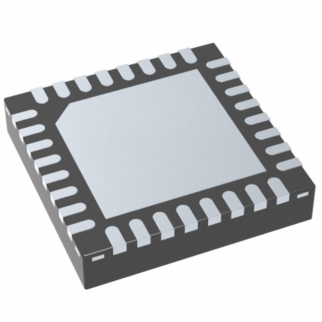


 工商网监
湘ICP备2023018690号
工商网监
湘ICP备2023018690号
