��
�
� �
��
���� �� � ��� ���
TPS54310-EP
www.ti.com ..................................................................................................................................................................................................... SLVS818 – APRIL 2008
3-V TO 6-V INPUT, 3-A OUTPUT, SYNCHRONOUS BUCK PWM
SWITCHER WITH INTEGRATED FETs (SWIFT™)
FEATURES
1
• Controlled Baseline
– One Assembly Site
– One Test Site
– One Fabrication Site
• Extended Temperature Performance of
–55°C to 125°C
• Enhanced Diminishing Manufacturing Sources
(DMS) Support
• Enhanced Product-Change Notification
• Qualification Pedigree (1)
• 60-mΩ MOSFET Switches for High Efficiency
at 3-A Continuous Output Source or Sink
Current
•
(1)
•
2
Component qualification in accordance with JEDEC and
industry standards to ensure reliable operation over an
extended temperature range. This includes, but is not limited
to, Highly Accelerated Stress Test (HAST) or biased 85/85,
temperature cycle, autoclave or unbiased HAST,
electromigration, bond intermetallic life, and mold compound
life. Such qualification testing should not be viewed as
justifying use of this component beyond specified
performance and environmental limits.
•
•
•
•
•
Adjustable Output Voltage Down to 0.9 V With
1% Accuracy
Externally Compensated for Design Flexibility
Fast Transient Response
Wide PWM Frequency: Fixed 350 kHz, 550
kHz, or Adjustable 280 kHz to 700 kHz
Load Protected by Peak Current Limit and
Thermal Shutdown
Integrated Solution Reduces Board Area and
Total Cost
APPLICATIONS
•
•
•
Low-Voltage High-Density Systems With
Power Distributed at 5 V or 3.3 V
Point of Load Regulation for
High-Performance DSPs, FPGAs, ASICs, and
Microprocessors
Broadband, Networking, and Optical
Communications Infrastructure
Portable Computing/Notebook PCs
DESCRIPTION/ORDERING INFORMATION
As members of the SWIFT™ family of dc/dc regulators, the TPS54310 low input voltage high output current
synchronous buck PWM converter integrates all required active components. Included on the substrate with the
listed features are a true, high performance, voltage error amplifier that provides high performance under
transient conditions; an undervoltage-lockout circuit to prevent start-up until the input voltage reaches 3 V; an
internally and externally set slow-start circuit to limit in-rush currents; and a power good output useful for
processor/logic reset, fault signaling, and supply sequencing.
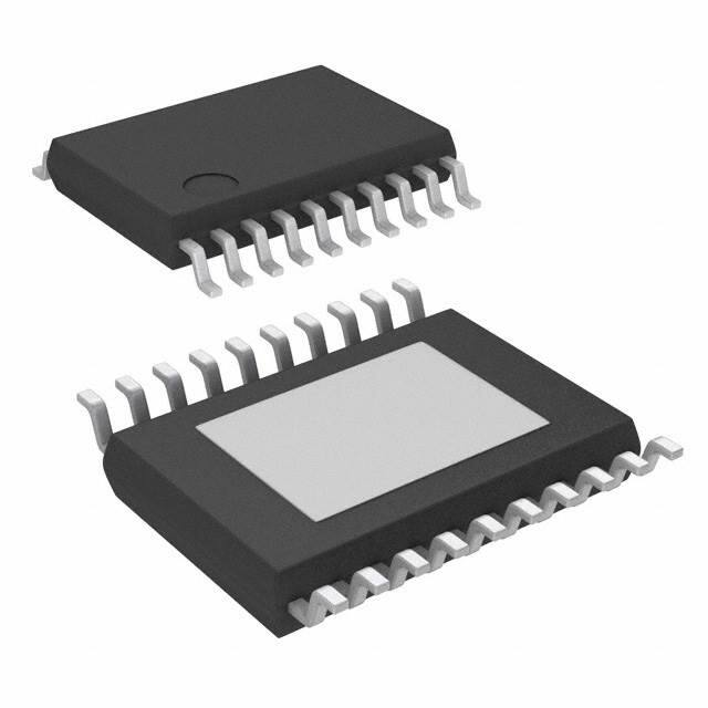
The TPS54310 device is available in a thermally enhanced 20-pin TSSOP (PWP) PowerPAD™ package, which
eliminates bulky heatsinks. TI provides evaluation modules and the SWIFT designer software tool to aid in
quickly achieving high-performance power supply designs to meet aggressive equipment development cycles.
1
2
Please be aware that an important notice concerning availability, standard warranty, and use in critical applications of
Texas Instruments semiconductor products and disclaimers thereto appears at the end of this data sheet.
SWIFT, PowerPAD are trademarks of Texas Instruments.
PRODUCTION DATA information is current as of publication date.
Products conform to specifications per the terms of the Texas
Instruments standard warranty. Production processing does not
necessarily include testing of all parameters.
Copyright © 2008, Texas Instruments Incorporated
�TPS54310-EP
SLVS818 – APRIL 2008 ..................................................................................................................................................................................................... www.ti.com
EFFICIENCY
vs
LOAD CURRENT
Simplified Schematic
Input
96
Output
VIN
PH
94
TPS54310
BOOT
92
Efficiency − %
PGND
VBIAS VSENSE
AGND COMP
90
88
86
84
TA = 25°C
VI = 5 V
VO = 3.3 V
82
80
0
0.5
1
1.5
2
2.5
3
Load Current − A
This integrated circuit can be damaged by ESD. Texas Instruments recommends that all integrated circuits be handled with
appropriate precautions. Failure to observe proper handling and installation procedures can cause damage.
ESD damage can range from subtle performance degradation to complete device failure. Precision integrated circuits may be more
susceptible to damage because very small parametric changes could cause the device not to meet its published specifications.
ORDERING INFORMATION (1)
(1)
(2)
(3)
TJ
OUTPUT VOLTAGE
PACKAGED DEVICES
PLASTIC HTSSOP (PWP) (2) (3)
TOPSIDE MARKING
–55°C to 125°C
Adjustable Down to 0.9 V
TPS54310MPWPREP
54310EP
For the most current package and ordering information, see the Package Option Addendum at the end of this document, or see the TI
website at www.ti.com.
Package drawings, thermal data, and symbolization are available at www.ti.com/packaging.
The PWP package is shipped taped and reeled with 2000 units per reel. See the application section of this data sheet for PowerPAD
drawing and layout information.
ABSOLUTE MAXIMUM RATINGS
over operating free-air temperature range (unless otherwise noted) (1)
VI
Input voltage range
VO
Output voltage range
IO
Output voltage range
Sink current
TPS54310
UNIT
VIN, SS/ENA, SYNC
–0.3 to 7
V
RT
–0.3 to 6
V
VSENSE
–0.3 to 4
V
BOOT
–0.3 to 17
V
VBIAS, PWRGD, COMP
–0.3 to 7
V
PH
–0.6 to 10
V
PH
Internally Limited
COMP, VBIAS
6
PH
6
A
COMP
6
mA
10
mA
±0.3
V
SS/ENA, PWRGD
Voltage differential
AGND to PGND
Continuous power dissipation
mA
See Package Dissipation Rating
TJ
Operating virtual-junction temperature range
–55 to 150
°C
Tstg
Storage temperature
–65 to 150
°C
(1)
2
Stresses beyond those listed under absolute maximum ratings may cause permanent damage to the device. These are stress ratings
only, and functional operation of the device at these or any other conditions beyond those indicated under recommended operating
conditions is not implied. Exposure to absolute-maximum-rated conditions for extended periods may affect device reliability.
Submit Documentation Feedback
Copyright © 2008, Texas Instruments Incorporated
Product Folder Link(s): TPS54310-EP
�TPS54310-EP
www.ti.com ..................................................................................................................................................................................................... SLVS818 – APRIL 2008
RECOMMENDED OPERATING CONDITIONS
MIN
VI
Input voltage
TJ
Operating virtual-junction temperature
PACKAGE DISSIPATION RATINGS (1)
MAX
UNIT
3
6
V
–55
125
°C
(2)
PACKAGE
THERMAL IMPEDANCE
JUNCTION-TO-AMBIENT
TA = 25°C
POWER RATING
TA = 70°C
POWER RATING
TA = 85°C
POWER RATING
20-Pin PWP with solder
26°C/W
3.85 W (3)
2.12 W
1.54 W
20-Pin PWP without solder
57.5°C/W
1.73 W
0.96 W
0.69 W
(1)
(2)
(3)
For more information on the PWP package, refer to TI technical brief, literature number SLMA002.
Test board conditions:
a. 3 inch × 3 inch, 2 layers, Thickness: 0.062 inch
b. 1.5 oz copper traces located on the top of the PCB
c. 1.5 oz copper ground plane on the bottom of the PCB
d. Ten thermal vias (see recommended land pattern in application section of this data sheet)
Maximum power dissipation may be limited by overcurrent protection.
ELECTRICAL CHARACTERISTICS
TJ = –55°C to 125°C, VIN = 3 V to 6 V (unless otherwise noted)
PARAMETER
TEST CONDITIONS
MIN
TYP
MAX
UNIT
SUPPLY VOLTAGE, VIN
VIN input voltage range
Quiescent current
3
6
fs = 350 kHz, SYNC = 0.8 V, RT open
6.2
9.6
fs = 550 kHz, SYNC ≥ 2.5 V, RT open, phase pin open
8.4
12.8
1
1.4
2.95
3
Shutdown, SS/ENA = 0 V
V
mA
UNDERVOLTAGE LOCKOUT
Start threshold voltage, UVLO
V
Stop threshold voltage, UVLO
2.70
2.80
Hysteresis voltage, UVLO
0.10
0.16
V
2.5
µs
Rising and falling edge deglitch, UVLO (1)
BIAS VOLTAGE
VO
Output voltage, VBIAS
I(VBIAS) = 0
2.70
2.80
Output current, VBIAS (2)
2.95
V
100
µA
0.900
V
CUMULATIVE REFERENCE
Vref
Accuracy
0.880
0.891
REGULATION
Line regulation (1)
Load regulation (1)
(1)
(2)
(3)
(3)
(3)
IL = 1.5 A, fs = 350 kHz, TJ = 85°C
0.07
IL = 1.5 A, fs = 550 kHz, TJ = 85°C
0.07
IL = 0 A to 3 A, fs = 350 kHz, TJ = 85°C
0.03
IL = 0 A to 3 A, fs = 550 kHz, TJ = 85°C
0.03
%/V
%/A
Specified by design
Static resistive loads only
Specified by the circuit used in Figure 10.
Submit Documentation Feedback
Copyright © 2008, Texas Instruments Incorporated
Product Folder Link(s): TPS54310-EP
3
�TPS54310-EP
SLVS818 – APRIL 2008 ..................................................................................................................................................................................................... www.ti.com
ELECTRICAL CHARACTERISTICS (continued)
TJ = –55°C to 125°C, VIN = 3 V to 6 V (unless otherwise noted)
PARAMETER
TEST CONDITIONS
MIN
TYP
MAX
SYNC ≤ 0.8 V, RT open
255
350
450
SYNC ≥ 2.5 V, RT open
400
550
700
RT = 180 kΩ (1% resistor to AGND) (4)
245
280
313
RT = 100 kΩ (1% resistor to AGND)
450
500
550
RT = 68 kΩ (1% resistor to AGND)
650
700
775
UNIT
OSCILLATOR
Internally set free-running frequency range
Externally set free-running frequency range
High-level threshold voltage, SYNC
2.5
kHz
V
Low-level threshold voltage, SYNC
Pulse duration, SYNC (5)
kHz
0.8
V
700
kHz
50
Frequency range, SYNC (5)
330
Ramp valley (4)
0.75
Ramp amplitude (peak-to-peak) (4)
V
1
Minimum controllable on time
V
200
Maximum duty cycle
ns
90%
ERROR AMPLIFIER
Error amplifier open loop voltage gain
1 kΩ COMP to AGND (5)
90
110
Error amplifier unity gain bandwidth
Parallel 10 kΩ, 160 pF COMP to AGND (5)
3
5
0
Error amplifier common-mode input voltage range
Powered by internal LDO (5)
IIB
Input bias current, VSENSE
VSENSE = Vref
VO
Output voltage slew rate (symmetric), COMP
60
dB
MHz
VBIAS
V
250
nA
1.4
V/µs
PWM COMPARATOR
PWM comparator propagation delay time, PWM
comparator input to PH pin (excluding dead time)
10 mV overdrive (5)
70
85
ns
1.20
1.45
V
SLOW-START/ENABLE
Enable threshold voltage, SS/ENA
0.82
Enable hysteresis voltage, SS/ENA (4)
Falling edge deglitch, SS/ENA (4)
Internal slow-start time
0.03
V
2.5
µs
2.2
3.35
4.1
Charge current, SS/ENA
SS/ENA = 0 V
2.5
5
8
ms
µA
Discharge current, SS/ENA
SS/ENA = 0.2 V, VI = 2.7 V
1.2
2.3
4
mA
POWER GOOD
Power good threshold voltage
VSENSE falling
Power good hysteresis voltage (4)
Power good falling edge deglitch (4)
90
%Vref
3
%Vref
35
Output saturation voltage, PWRGD
I(sink) = 2.5 mA
Leakage current, PWRGD
VI = 5.0 V
0.18
µs
0.30
V
1
µA
CURRENT LIMIT
Current limit trip point
VI = 3 V, output shorted (5)
4
6.5
VI = 6 V, output shorted (5)
4.5
7.5
A
Current limit leading edge blanking time (4)
100
ns
Current limit total response time (4)
200
ns
THERMAL SHUTDOWN
Thermal shutdown trip point (4)
135
Thermal shutdown hysteresis (4)
150
165
°C
°C
10
OUTPUT POWER MOSFETS
rDS(on)
(4)
(5)
(6)
4
Power MOSFET switches
IO = 0.5 A, VI = 6 V (6)
59
88
IO = 0.5 A, VI = 3 V (6)
85
136
mΩ
Specified by design
Specified by design for TJ = -40°C to 125°C
Matched MOSFETs, low side rDS(on) production tested, high side rDS(on) specified by design.
Submit Documentation Feedback
Copyright © 2008, Texas Instruments Incorporated
Product Folder Link(s): TPS54310-EP
�TPS54310-EP
www.ti.com ..................................................................................................................................................................................................... SLVS818 – APRIL 2008
PIN ASSIGNMENTS
PWP PACKAGE
(TOP VIEW)
AGND
VSENSE
COMP
PWRGD
BOOT
PH
PH
PH
PH
PH
1
2
3
4
5
6
7
8
9
10
20
19
18
17
16
15
14
13
12
11
RT
SYNC
SS/ENA
VBIAS
VIN
VIN
VIN
PGND
PGND
PGND
TERMINAL FUNCTIONS
TERMINAL
DESCRIPTION
NAME
NO.
AGND
1
Analog ground. Return for compensation network/output divider, slow-start capacitor, VBIAS capacitor, RT resistor
and SYNC pin. Make PowerPAD connection to AGND.
BOOT
5
Bootstrap input. 0.022 µF to 0.1 µF low-ESR capacitor connected from BOOT to PH generates floating drive for the
high-side FET driver.
COMP
3
Error amplifier output. Connect compensation network from COMP to VSENSE.
PGND
11–13
Power ground. High current return for the low-side driver and power MOSFET. Connect PGND with large copper
areas to the input and output supply returns, and negative terminals of the input and output capacitors.
PH
6–10
Phase input/output. Junction of the internal high and low-side power MOSFETs, and output inductor.
PWRGD
4
Power good open drain output. High when VSENSE ≥ 90% Vref, otherwise PWRGD is low. Note that output is low
when SS/ENA is low or internal shutdown signal active.
RT
20
Frequency setting resistor input. Connect a resistor from RT to AGND to set the switching frequency, fs.
SS/ENA
18
Slow-start/enable input/output. Dual function pin which provides logic input to enable/disable device operation and
capacitor input to externally set the start-up time.
SYNC
19
Synchronization input. Dual function pin which provides logic input to synchronize to an external oscillator or pin
select between two internally set switching frequencies. When used to synchronize to an external signal, a resistor
must be connected to the RT pin.
VBIAS
17
Internal bias regulator output. Supplies regulated voltage to internal circuitry. Bypass VBIAS pin to AGND pin with a
high quality, low ESR 0.1 µF to 1.0 µF ceramic capacitor.
VIN
VSENSE
14–16
2
Input supply for the power MOSFET switches and internal bias regulator. Bypass VIN pins to PGND pins close to
device package with a high quality, low ESR 1-µF to 10-µF ceramic capacitor.
Error amplifier inverting input.
Submit Documentation Feedback
Copyright © 2008, Texas Instruments Incorporated
Product Folder Link(s): TPS54310-EP
5
�TPS54310-EP
SLVS818 – APRIL 2008 ..................................................................................................................................................................................................... www.ti.com
FUNCTIONAL BLOCK DIAGRAM
VBIAS
AGND
VIN
Enable
Comparator
SS/ENA
Falling
Edge
Deglitch
1.2 V
Hysteresis: 0.03
V
2.5 µs
VIN UVLO
Comparator
VIN
2.95 V
Hysteresis: 0.16
V
REG
VBIAS
SHUTDOWN
VIN
ILIM
Comparator
Thermal
Shutdown
150°C
3−6V
Leading
Edge
Blanking
Falling
and
Rising
Edge
Deglitch
100 ns
BOOT
30 mΩ
2.5 µs
SS_DIS
SHUTDOWN
Internal/External
Slow-start
(Internal Slow-start Time = 3.35 ms
PH
+
−
R Q
Error
Amplifier
Reference
VREF = 0.891 V
S
PWM
Comparator
LOUT
VO
CO
Adaptive Dead-Time
and
Control Logic
VIN
30 mΩ
OSC
PGND
Powergood
Comparator
PWRGD
VSENSE
Falling
Edge
Deglitch
0.90 Vref
TPS54610
Hysteresis: 0.03 Vref
VSENSE
COMP
RT
SHUTDOWN
35 µs
SYNC
ADDITIONAL 3-A SWIFT DEVICES
DEVICE
OUTPUT VOLTAGE
DEVICE
OUTPUT VOLTAGE
DEVICE
TPS54311
0.9 V
TPS54314
1.8 V
TPS54372
OUTPUT VOLTAGE
DDR/Adjustable
TPS54312
1.2 V
TPS54315
2.5 V
TPS54373
Prebias/Adjustable
TPS54313
1.5 V
TPS54316
3.3 V
TPS54380
Sequencing/Adjustable
RELATED DC/DC PRODUCTS
•
•
•
6
TPS40000 — dc/dc controller
PT5500 series — 3-A plug-in modules
TPS757xx — 3-A low dropout regulator
Submit Documentation Feedback
Copyright © 2008, Texas Instruments Incorporated
Product Folder Link(s): TPS54310-EP
�TPS54310-EP
www.ti.com ..................................................................................................................................................................................................... SLVS818 – APRIL 2008
TYPICAL CHARACTERISTICS
DRAIN-SOURCE ON-STATE
RESISTANCE
vs
JUNCTION TEMPERATURE
DRAIN-SOURCE ON-STATE
RESISTANCE
vs
JUNCTION TEMPERATURE
VI = 3.3 V
100
IO = 3 A
80
60
40
20
VI = 5 V
60
40
20
0
−40
0
25
85
IO = 3 A
80
0
−40
125
85
550
450
SYNC ≤ 0.8 V
350
250
−40
125
0
25
85
125
TJ − Junction Temperature − °C
Figure 2.
Figure 3.
EXTERNALLY SET OSCILLATOR
FREQUENCY
vs
JUNCTION TEMPERATURE
VOLTAGE REFERENCE
vs
JUNCTION TEMPERATURE
OUTPUT VOLTAGE REGULATION
vs
INPUT VOLTAGE
0.8950
0.895
800
Vref − Voltage Reference − V
700
600
RT = 100 k
500
400
RT = 180 k
300
200
−40
0
25
85
0.893
0.891
0.889
0.887
0.885
−40
125
TA = 85°C
0.8930
0.8910
0.8890
f = 350 kHz
0.8870
0.8850
0
25
85
125
3
4
5
VI − Input Voltage − V
TJ − Junction Temperature − °C
TJ − Junction Temperature − °C
Figure 4.
Figure 5.
Figure 6.
ERROR AMPLIFIER
OPEN LOOP RESPONSE
INTERNAL SLOW-START TIME
vs
JUNCTION TEMPERATURE
DEVICE POWER LOSSES
vs
LOAD CURRENT
0
100
−40
−60
80
Phase
−80
−100
60
−120
40
Gain
20
−140
−160
0
−180
−20
100
1k
−200
10 k 100 k 1 M 10 M
f − Frequency − Hz
Figure 7.
TJ − 125°C
fs = 700 kHz
2
3.65
Device Power Losses − W
120
6
2.25
3.80
−20
Internal Slow-Start Time − ms
RL= 10 kΩ,
CL = 160 pF,
TA = 25°C
10
VO − Output Voltage Regulation − V
RT = 68 k
0
SYNC ≥ 2.5 V
Figure 1.
140
Gain − dB
25
650
TJ − Junction Temperature − °C
Phase − Degrees
f − Externally Set Oscillator Frequency − kHz
TJ − Junction Temperature − °C
0
750
f − Internally Set Oscillator Frequency −kHz
100
Drain-Source On-State Resistance − Ω
Drain-Source On-State Resistance − Ω
120
INTERNALLY SET OSCILLATOR
FREQUENCY
vs
JUNCTION TEMPERATURE
1.75
3.50
3.35
1.5
VI = 3.3 V
1.25
3.20
1
VI = 5 V
0.75
3.05
2.90
2.75
−40
0.5
0.25
0
25
85
TJ − Junction Temperature − °C
125
Figure 8.
0
0
1
2
3
IL − Load Current − A
Figure 9.
Submit Documentation Feedback
Copyright © 2008, Texas Instruments Incorporated
Product Folder Link(s): TPS54310-EP
4
7
�TPS54310-EP
SLVS818 – APRIL 2008 ..................................................................................................................................................................................................... www.ti.com
APPLICATION INFORMATION
Figure 10 shows the schematic diagram for a typical TPS54310 application. The TPS54310 (U1) can provide up
to 3 A of output current at a nominal output voltage of 3.3 V. For proper thermal performance, the thermal pad
under the TPS54310 integrated circuit needs to be soldered well to the printed-circuit board.
J1
VI
GND
VIN
2
1
C2
+
U1
TPS54310PWP
R3
1
R1
10 kΩ
20
71.5 kΩ
19
18
17
C3
0.1 µF
4
PWRGD
RT
15
VIN
2
PH
6
5
BOOT
13
PGND
C6
2700 pF
R5
VO
GND
C11
1000 pF
C7
0.047 µF
11
PGND
PwrPAD
R4
3.74 kΩ
C9
180 µF
4V
J3
12
PGND
C5
3900 pF
C4
100 pF
R2
3.74 kΩ
2
+
8
7
PH
VSENSE
AGND
9
PH
PH
1
10
PH
VBIAS
PWRGD
L1
1.2 µH
14
VIN
SS/ENA
3 COMP
1
16
VIN
SYNC
C8
10 µF
R6
R7
732 Ω
49.9 Ω
10 kΩ
1
Optional
Figure 10. TPS54310 Schematic
INPUT VOLTAGE
SETTING THE OUTPUT VOLTAGE
The input to the circuit is a nominal 5 VDC, applied at
J1. The optional input filter (C2) is a 220-µF POSCAP
capacitor, with a maximum allowable ripple current of
3 A. C8 is the decoupling capacitor for the TPS54310
and must be located as close to the device as
possible.
The output voltage of the TPS54310 can be set by
feeding back a portion of the output to the VSENSE
pin using a resistor divider network. In the application
circuit of Figure 10, this divider network is comprised
of resistors R5 and R4. To calculate the resistor
values to generate the required output voltage use
Equation 1.
R5 x 0.891
R4 =
VO - 0.891
(1)
FEEDBACK CIRCUIT
The resistor divider network of R5 and R4 sets the
output voltage for the circuit at 3.3 V. R5, along with
R2, R6, C4, C5, and C6 forms the loop compensation
network for the circuit. For this design, a Type 3
topology is used.
8
Start with a fixed value of R5 and calculate the
required R4 value. Assuming a fixed value of 10 kΩ
for R5, the following table gives the appropriate R4
value for several common output voltages:
OUTPUT VOLTAGE (V)
R4 VALUE (KΩ)
1.2
28.7
1.5
14.7
1.8
9.76
2.5
5.49
3.3
3.74
Submit Documentation Feedback
Copyright © 2008, Texas Instruments Incorporated
Product Folder Link(s): TPS54310-EP
�TPS54310-EP
www.ti.com ..................................................................................................................................................................................................... SLVS818 – APRIL 2008
OPERATING FREQUENCY
In the application circuit, the 350-kHz operation is
selected by leaving RT and SYNC open. Connecting
a 68-kΩ to 180-kΩ resistor between RT (pin 20) and
analog ground can be used to set the switching
frequency from 280 kHz to 700 kHz. To calculate the
RT resistor, use the Equation 2:
R + 100 kW 500 kHz
ƒ
SW
(2)
OUTPUT FILTER
The output filter is composed of a 1.2-µH inductor
and 180-µF capacitor. The inductor is a low dc
resistance (0.017 Ω) type, Coilcraft DO1813P-122HC.
The capacitor used is a 4-V special polymer type with
a maximum ESR of 0.015 Ω. The feedback loop is
compensated so that the unity gain frequency is
approximately 75 kHz.
PCB LAYOUT
Figure 11 shows a generalized PCB layout guide for
the TPS54310.
The VIN pins should be connected together on the
printed circuit board (PCB) and bypassed with a low
ESR ceramic bypass capacitor. Care should be taken
to minimize the loop area formed by the bypass
capacitor connections, the VIN pins, and the
TPS54X10 ground pins. The minimum recommended
bypass capacitance is 10-µF ceramic with a X5R or
X7R dielectric and the optimum placement is closest
to the VIN pins and the PGND pins.
The TPS54310 has two internal grounds (analog and
power). Inside the TPS54310, the analog ground ties
to all of the noise sensitive signals, while the power
ground ties to the noisier power signals. Noise
injected between the two grounds can degrade the
performance of the TPS54310, particularly at higher
output currents. Ground noise on an analog ground
plane can also cause problems with some of the
control and bias signals. For these reasons, separate
analog and power ground traces are recommended.
There should be an area of ground one the top layer
directly under the IC, with an exposed area for
connection to the PowerPAD. Use vias to connect
this ground area to any internal ground planes. Use
additional vias at the ground side of the input and
output filter capacitors as well. The AGND and PGND
pins should be tied to the PCB ground by connecting
them to the ground area under the device as shown.
The only components that should tie directly to the
power ground plane are the input capacitors, the
output capacitors, the input voltage decoupling
capacitor, and the PGND pins of the TPS54310. Use
a separate wide trace for the analog ground signal
path. This analog ground should be used for the
voltage set point divider, timing resistor RT, slow start
capacitor and bias capacitor grounds. Connect this
trace directly to AGND (pin 1).
The PH pins should be tied together and routed to
the output inductor. Since the PH connection is the
switching node, inductor should be located very close
to the PH pins and the area of the PCB conductor
minimized to prevent excessive capacitive coupling.
Connect the boot capacitor between the phase node
and the BOOT pin as shown. Keep the boot capacitor
close to the IC and minimize the conductor trace
lengths.
Connect the output filter capacitor(s) as shown
between the VOUT trace and PGND. It is important to
keep the loop formed by the PH pins, Lout, Cout and
PGND as small as practical.
Place the compensation components from the VOUT
trace to the VSENSE and COMP pins. Do not place
these components too close to the PH trace. Due to
the size of the IC package and the device pinout,
they will have to be routed somewhat close, but
maintain as much separation as possible while still
keeping the layout compact.
Connect the bias capacitor from the VBIAS pin to
analog ground using the isolated analog ground
trace. If a slow-start capacitor or RT resistor is used,
or if the SYNC pin is used to select 350-kHz
operating frequency, connect them to this trace as
well.
Submit Documentation Feedback
Copyright © 2008, Texas Instruments Incorporated
Product Folder Link(s): TPS54310-EP
9
�TPS54310-EP
SLVS818 – APRIL 2008 ..................................................................................................................................................................................................... www.ti.com
ANALOG GROUND TRACE
FREQUENCY SET RESISTOR
AGND
RT
SYNC
VSENSE
COMPENSATION
NETWORK
COMP
SS/ENA
PWRGD
BOOT
CAPACITOR
BOOT
SLOW START
CAPACITOR
VBIAS
EXPOSED
POWERPAD
AREA
BIAS CAPACITOR
VIN
PH
VIN
PH
VIN
PH
PGND
PH
PGND
PH
PGND
Vin
VOUT
OUTPUT INDUCTOR
PH
INPUT
BYPASS
CAPACITOR
OUTPUT
FILTER
CAPACITOR
INPUT
BULK
FILTER
TOPSIDE GROUND AREA
VIA to Ground Plane
Figure 11. TPS54310 PCB Layout
LAYOUT CONSIDERATIONS FOR THERMAL
PERFORMANCE
For operation at full rated load current, the analog
ground plane must provide adequate heat dissipating
area. A 3 inch by 3 inch plane of 1 ounce copper is
recommended, though not mandatory, depending on
ambient temperature and airflow. Most applications
have larger areas of internal ground plane available,
and the PowerPAD should be connected to the
largest area available. Additional areas on the top or
bottom layers also help dissipate heat, and any area
available should be used when 3 A or greater
operation is desired. Connection from the exposed
area of the PowerPAD to the analog ground plane
layer should be made using 0.013 inch diameter vias
to avoid solder wicking through the vias. Six vias
should be in the PowerPAD area with four additional
vias located under the device package. The size of
the vias under the package, but not in the exposed
thermal pad area, can be increased to 0.018.
Additional vias beyond the ten recommended that
enhance thermal performance should be included in
areas not under the device package.
10
Submit Documentation Feedback
Copyright © 2008, Texas Instruments Incorporated
Product Folder Link(s): TPS54310-EP
�TPS54310-EP
www.ti.com ..................................................................................................................................................................................................... SLVS818 – APRIL 2008
6 PL ∅ 0.0130
4 PL ∅ 0.0180
Connect Pin 1 to Analog Ground Plane
in This Area for Optimum Performance
0.0227
0.0600
0.0400
0.2560
0.2454
0.0400
0.0600
Minimum Recommended Top
Side Analog Ground Area
Minimum Recommended Thermal Vias: 6 × .013 dia.
Inside Powerpad Area 4 × .018 dia. Under Device as Shown.
Additional .018 dia. Vias May be Used if Top Side Analog
Ground Area is Extended.
ÎÎÎ
ÎÎÎ
ÎÎÎ
ÎÎÎ
ÎÎÎ
ÎÎÎ
ÎÎÎ
ÎÎÎ
0.0150
0.06
0.1010
0.0256
0.1700
0.1340
0.0620
0.0400
Minimum Recommended Exposed
Copper Area For Powerpad. 5mm
Stencils may Require 10 Percent
Larger Area
Figure 12. Recommended Land Pattern for 20-Pin PWP PowerPAD
Submit Documentation Feedback
Copyright © 2008, Texas Instruments Incorporated
Product Folder Link(s): TPS54310-EP
11
�TPS54310-EP
SLVS818 – APRIL 2008 ..................................................................................................................................................................................................... www.ti.com
PERFORMANCE GRAPHS
EFFICIENCY
vs
OUTPUT CURRENT
OUTPUT VOLTAGE
vs
LOAD CURRENT
VI = 4 V
VI = 6 V
85
80
75
70
Phase
40
90
3.36
3.34
Gain − dB
VO − Output Voltage − %
Efficiency − %
TA = 25°C
VI = 5 V
3.38
90
135
60
VI = 5 V
95
65
LOOP RESPONSE
3.4
3.32
3.3
45
20
Gain
0
0
TA = 25°C
3.28
Phase − Degrees
100
−45
−20
3.26
0
1
2
3
4
−40
3.24
5
0
1
IO − Output Current − A
2
3
4
5
IL − Load Current − A
100
1k
10 k
100 k
f − Frequency − Hz
Figure 13.
Figure 14.
Figure 15.
OUTPUT RIPPLE VOLTAGE
LOAD TRANSIENT RESPONSE
SLOW-START TIMING
VI = 5 V
40 µs/div
VO (AC)
10 mV/div
−90
1M
VO (AC)
50 mV/div
VI 2 V/div
VO 2 V/div
VPWRGD 5 V/div
IO
2 A/div
VI = 5 V
IO = 3 A
400 ns/div
1 ms/div
Figure 16.
Figure 17.
Figure 18.
AMBIENT TEMPERATURE
vs
LOAD CURRENT
125
T A − Ambient Temperature − ° C
115
VI = 5 V
105
95
85
VI = 3.3 V
75
Safe Operating Area†
65
55
45
35
25
0
†
1
2
3
IL − Load Current − A
4
Safe operating area is applicable to the test board conditions
listed in the dissipation rating table section of this data sheet.
Figure 19.
12
Submit Documentation Feedback
Copyright © 2008, Texas Instruments Incorporated
Product Folder Link(s): TPS54310-EP
�TPS54310-EP
www.ti.com ..................................................................................................................................................................................................... SLVS818 – APRIL 2008
VBIAS Regulator (VBIAS)
DETAILED DESCRIPTION
Under Voltage Lock Out (UVLO)
The TPS54310 incorporates an under voltage lockout
circuit to keep the device disabled when the input
voltage (VIN) is insufficient. During power up, internal
circuits are held inactive until VIN exceeds the
nominal UVLO threshold voltage of 2.95 V. Once the
UVLO start threshold is reached, device start-up
begins. The device operates until VIN falls below the
nominal UVLO stop threshold of 2.8 V. Hysteresis in
the UVLO comparator, and a 2.5-µs rising and falling
edge deglitch circuit reduce the likelihood of shutting
the device down due to noise on VIN.
The VBIAS regulator provides internal analog and
digital blocks with a stable supply voltage over
variations in junction temperature and input voltage. A
high quality, low-ESR, ceramic bypass capacitor is
required on the VBIAS pin. X7R or X5R grade
dielectrics are recommended because their values
are more stable over temperature. The bypass
capacitor should be placed close to the BVIAS pin
and returned to AGND. External loading on VBIAS is
allowed, with the caution that internal circuits require
a minimum BVIAS of 2.7 V, and external loads on
VBIAS with ac or digital switching noise may degrade
performance. The VBIAS pin may be useful as a
reference voltage for external circuits.
Slow-Start/Enable (SS/ENA)
The slow-start/enable pin provides two functions; first,
the pin acts as an enable (shutdown) control by
keeping the device turned off until the voltage
exceeds the start threshold voltage of approximately
1.2 V. When SS/ENA exceeds the enable threshold,
device start up begins. The reference voltage fed to
the error amplifier is linearly ramped up from 0 V to
0.891 V in 3.35 ms. Similarly, the converter output
voltage reaches regulation in approximately 3.35 ms.
Voltage hysteresis and a 2.5-µs falling edge deglitch
circuit reduce the likelihood of triggering the enable
due to noise.
The second function of the SS/ENA pin provides an
external means of extending the slow-start time with
a low-value capacitor connected between SS/ENA
and AGND. Adding a capacitor to the SS/ENA pin
has two effects on start-up. First, a delay occurs
between release of the SS/ENA pin and start up of
the output. The delay is proportional to the slow-start
capacitor value and lasts until the SS/ENA pin
reaches the enable threshold. The start-up delay is
approximately:
1.2 V
td + C
(SS)
5 mA
(3)
Second, as the output becomes active, a brief
ramp-up at the internal slow-start rate may be
observed before the externally set slow-start rate
takes control and the output rises at a rate
proportional to the slow-start capacitor. The slow-start
time set by the capacitor is approximately:
0.7 V
t
+C
(SS)
(SS)
5 mA
(4)
Voltage Reference
The voltage reference system produces a precise Vref
signal by scaling the output of a temperature stable
bandgap circuit. During manufacture, the bandgap
and scaling circuits are trimmed to produce 0.891 V
at the output of the error amplifier, with the amplifier
connected as a voltage follower. The trim procedure
adds to the high precision regulation of the
TPS54310, since it cancels offset errors in the scale
and error amplifier circuits
Oscillator and PWM Ramp
The oscillator frequency can be set to internally fixed
values of 350 kHz or 550 kHz using the SYNC pin as
a static digital input. If a different frequency of
operation is required for the application, the oscillator
frequency can be externally adjusted from 280 kHz to
700 kHz by connecting a resistor to the RT pin to
ground and floating the SYNC pin. The switching
frequency is approximated by the following equation,
where R is the resistance from RT to AGND:
SWITCHING FREQUENCY + 100 kW
R
500 kHz
(5)
External synchronization of the PWM ramp is
possible over the frequency range of 330 kHz to
700 kHz by driving a synchronization signal into
SYNC and connecting a resistor from RT to AGND.
Choose an RT resistor that sets the free-running
frequency to 80% of the synchronization signal.
Table 1 summarizes the frequency selection
configurations.
The actual slow-start is likely to be less than the
above approximation due to the brief ramp-up at the
internal rate.
Submit Documentation Feedback
Copyright © 2008, Texas Instruments Incorporated
Product Folder Link(s): TPS54310-EP
13
�TPS54310-EP
SLVS818 – APRIL 2008 ..................................................................................................................................................................................................... www.ti.com
Table 1. Summary of the Frequency Selection Configurations
SWITCHING FREQUENCY
SYNC PIN
RT PIN
350 kHz, internally set
Float or AGND
Float
550 kHz, internally set
≥ 2.5 V
Float
Externally set 280 kHz to 700 kHz
Float
R = 68 k to 180 k
Externally synchronized frequency
Synchronization signal
R = RT value for 80% of external synchronization frequency
Error Amplifier
The high performance, wide bandwidth, voltage error
amplifier sets the TPS54310 apart from most dc/dc
converters. The user is given the flexibility to use a
wide range of output L and C filter components to suit
the particular needs of the application. Type 2 or type
3 compensation can be employed using external
compensation components.
PWM Control
Signals from the error amplifier output, oscillator, and
current limit circuit are processed by the PWM control
logic. Referring to the internal block diagram, the
control logic includes the PWM comparator, OR gate,
PWM latch, and portions of the adaptive dead-time
and control logic block. During steady-state operation
below the current limit threshold, the PWM
comparator output and oscillator pulse train
alternately reset and set the PWM latch. Once the
PWM latch is set, the low-side FET remains on for a
minimum duration set by the oscillator pulse duration.
During this period, the PWM ramp discharges rapidly
to its valley voltage. When the ramp begins to charge
back up, the low-side FET turns off and high-side
FET turns on. As the PWM ramp voltage exceeds the
error amplifier output voltage, the PWM comparator
resets the latch, thus turning off the high-side FET
and turning on the low-side FET. The low-side FET
remains on until the next oscillator pulse discharges
the PWM ramp.
During transient conditions, the error amplifier output
could be below the PWM ramp valley voltage or
above the PWM peak voltage. If the error amplifier is
high, the PWM latch is never reset and the high-side
FET remains on until the oscillator pulse signals the
control logic to turn the high-side FET off and the
low-side FET on. The device operates at its
maximum duty cycle until the output voltage rises to
the regulation set-point, setting VSENSE to
approximately the same voltage as Vref. If the error
amplifier output is low, the PWM latch is continually
reset and the high-side FET does not turn on. The
14
low-side FET remains on until the VSENSE voltage
decreases to a range that allows the PWM
comparator to change states. The TPS54310 is
capable of sinking current continuously until the
output reaches the regulation set-point.
If the current limit comparator trips for longer than
100 ns, the PWM latch resets before the PWM ramp
exceeds the error amplifier output. The high-side FET
turns off and low-side FET turns on to decrease the
energy in the output inductor and consequently the
output current. This process is repeated each cycle in
which the current limit comparator is tripped.
Dead-Time Control and MOSFET Drivers
Adaptive dead-time control prevents shoot-through
current from flowing in both N-channel power
MOSFETs during the switching transitions by actively
controlling the turn-on times of the MOSFET drivers.
The high-side driver does not turn on until the gate
drive voltage to the low-side FET is below 2 V. The
low-side driver does not turn on until the voltage at
the gate of the high-side MOSFETs is below 2 V. The
high-side and low-side drivers are designed with
300-mA source and sink capability to quickly drive the
power MOSFETs gates. The low-side driver is
supplied from VIN, while the high-side drive is
supplied from the BOOT pin. A bootstrap circuit uses
an external BOOT capacitor and an internal 2.5-Ω
bootstrap switch connected between the VIN and
BOOT pins. The integrated bootstrap switch improves
drive efficiency and reduces external component
count.
Overcurrent Protection
The cycle by cycle current limiting is achieved by
sensing the current flowing through the high-side
MOSFET and differential amplifier and comparing it to
the preset overcurrent threshold. The high-side
MOSFET is turned off within 200 ns of reaching the
current limit threshold. A 100-ns leading edge
blanking circuit prevents false tripping of the current
limit. Current limit detection occurs only when current
flows from VIN to PH when sourcing current to the
output filter. Load protection during current sink
operation is provided by thermal shutdown.
Submit Documentation Feedback
Copyright © 2008, Texas Instruments Incorporated
Product Folder Link(s): TPS54310-EP
�TPS54310-EP
www.ti.com ..................................................................................................................................................................................................... SLVS818 – APRIL 2008
Thermal Shutdown
Power Good (PWRGD)
The device uses the thermal shutdown to turn off the
power MOSFETs and disable the controller if the
junction temperature exceeds 150°C. The device is
released from shutdown when the junction
temperature decreases to 10°C below the thermal
shutdown trip point and starts up under control of the
slow-start circuit. Thermal shutdown provides
protection when an overload condition is sustained for
several milliseconds. With a persistent fault condition,
the device cycles continuously; starting up by control
of the soft-start circuit, heating up due to the fault,
and then shutting down upon reaching the thermal
shutdown point.
The power good circuit monitors for under voltage
conditions on VSENSE. If the voltage on VSENSE is
10% below the reference voltage, the open-drain
PWRGD output is pulled low. PWRGD is also pulled
low if VIN is less than the UVLO threshold, or
SS/ENA is low, or thermal shutdown is asserted.
When VIN = UVLO threshold, SS/ENA = enable
threshold, and VSENSE > 90% of Vref, the open drain
output of the PWRGD pin is high. A hysteresis
voltage equal to 3% of Vref and a 35-µs falling edge
deglitch circuit prevent tripping of the power good
comparator due to high frequency noise.
Submit Documentation Feedback
Copyright © 2008, Texas Instruments Incorporated
Product Folder Link(s): TPS54310-EP
15
�PACKAGE MATERIALS INFORMATION
www.ti.com
12-Feb-2019
TAPE AND REEL INFORMATION
*All dimensions are nominal
Device
TPS54310MPWPREP
Package Package Pins
Type Drawing
SPQ
HTSSOP
2000
PWP
20
Reel
Reel
A0
Diameter Width (mm)
(mm) W1 (mm)
330.0
16.4
Pack Materials-Page 1
6.95
B0
(mm)
K0
(mm)
P1
(mm)
7.1
1.6
8.0
W
Pin1
(mm) Quadrant
16.0
Q1
�PACKAGE MATERIALS INFORMATION
www.ti.com
12-Feb-2019
*All dimensions are nominal
Device
Package Type
Package Drawing
Pins
SPQ
Length (mm)
Width (mm)
Height (mm)
TPS54310MPWPREP
HTSSOP
PWP
20
2000
350.0
350.0
43.0
Pack Materials-Page 2
����IMPORTANT NOTICE AND DISCLAIMER
TI PROVIDES TECHNICAL AND RELIABILITY DATA (INCLUDING DATASHEETS), DESIGN RESOURCES (INCLUDING REFERENCE
DESIGNS), APPLICATION OR OTHER DESIGN ADVICE, WEB TOOLS, SAFETY INFORMATION, AND OTHER RESOURCES “AS IS”
AND WITH ALL FAULTS, AND DISCLAIMS ALL WARRANTIES, EXPRESS AND IMPLIED, INCLUDING WITHOUT LIMITATION ANY
IMPLIED WARRANTIES OF MERCHANTABILITY, FITNESS FOR A PARTICULAR PURPOSE OR NON-INFRINGEMENT OF THIRD
PARTY INTELLECTUAL PROPERTY RIGHTS.
These resources are intended for skilled developers designing with TI products. You are solely responsible for (1) selecting the appropriate
TI products for your application, (2) designing, validating and testing your application, and (3) ensuring your application meets applicable
standards, and any other safety, security, or other requirements. These resources are subject to change without notice. TI grants you
permission to use these resources only for development of an application that uses the TI products described in the resource. Other
reproduction and display of these resources is prohibited. No license is granted to any other TI intellectual property right or to any third
party intellectual property right. TI disclaims responsibility for, and you will fully indemnify TI and its representatives against, any claims,
damages, costs, losses, and liabilities arising out of your use of these resources.
TI’s products are provided subject to TI’s Terms of Sale (www.ti.com/legal/termsofsale.html) or other applicable terms available either on
ti.com or provided in conjunction with such TI products. TI’s provision of these resources does not expand or otherwise alter TI’s applicable
warranties or warranty disclaimers for TI products.
Mailing Address: Texas Instruments, Post Office Box 655303, Dallas, Texas 75265
Copyright © 2019, Texas Instruments Incorporated
�


 工商网监
湘ICP备2023018690号
工商网监
湘ICP备2023018690号
