Order
Now
Product
Folder
Support &
Community
Tools &
Software
Technical
Documents
TPS546C20A
SLUSCK1C – JULY 2016 – REVISED JUNE 2018
TPS546C20A 4.5-V to 18-V, 35-A 2× Stackable Synchronous Buck Converters
With PMBus Supporting Telemetry
1 Features
2 Applications
•
•
•
•
1
•
•
•
•
•
•
•
•
•
•
•
•
•
•
•
•
•
•
PMBus™ 1.3 Compliant Converters: 35 A
2-Device Stackable for up to 70 A With Current
Sharing
Input Voltage Range: 4.5 V to 18 V
Output Voltage Range: 0.35 V to 5.5 V
Integrated 3.2-mΩ and 1.4-mΩ Stacked
NexFET™ Power Stage
350-mV to 1650-mV Reference for Adaptive
Voltage Scaling (AVS) Function and Margining
through PMBus
0.5% Reference Accuracy at 600 mV and Above
Lossless Low-Side MOSFET Current Sensing
Voltage Mode Control With Input Feed-Forward
Differential Remote Sensing
Monotonic Start-Up into Pre-Biased Output
Output Voltage and Output Current Reporting
Internal Die Temperature Monitoring
2 PMBus Addresses (Master 36d/Slave 37d)
Selectable Boot-up Vout and Soft Start Values via
Pin-Strapping
Programmable via the PMBus Interface:
– OCP, UVLO, Soft-Start, PG, OV, UV, OT
Levels, Fault Responses
– Turnon and Turnoff Delays
Thermal Shutdown
Pin Strapping for Switching Frequency: 200 kHz to
1 MHz
Frequency Synchronization to an External Clock
or Output Clock to Sync Out
Create a Custom Design Using the TPS546C20A
With the WEBENCH® Power Designer
Test and Instrumentation
Ethernet Switches, Optical Switches, Routers,
Base Stations
Servers
Enterprise Storage SSD
•
•
3 Description
The TPS546C20A devices are PMBus 1.3 Compliant,
non-isolated DC/DC converters with integrated FETs,
capable of high-frequency operation and 35-A current
output from a 7-mm × 5-mm package. Two
TPS546C20A devices can be paralleled together to
provide up to 70-A load. Current sensing is realized
by sampling a small portion of the power stage
current and independent on the device temperature.
High-frequency, low-loss switching, provided by an
integrated NexFET power stage and optimized
drivers, allows for very high-density power solutions.
The PMBus interface enables the AVS functions
through VOUT_COMMAND, flexible converter
configuration, as well as key parameters monitoring
including output voltage, current, and internal die
temperature. Response to fault conditions can be set
to either restart, latch-off or ignore depending on
system requirements.
Device Information(1)
DEVICE NAME
TPS546C20A
PACKAGE
LQFN (40)
BODY SIZE
7.00 mm × 5.00 mm
(1) For all available packages, see the orderable addendum at
the end of the data sheet.
.
Simplified Application
BP3
VIN
DIFFO
FB
PVIN
RESET/PGD
AVIN
VOUT
COMP
BOOT
RT
TPS546C20A
SW
VSEL
SMB_ALERT
PMB_CLK
CNTL
SYNC
VSHARE
ISHARE
AGND
PMB_DATA
BP6
SS
BP3
RSP
RSN
+
LOAD
±
PGND
DRGND
Copyright © 2016, Texas Instruments Incorporated
1
An IMPORTANT NOTICE at the end of this data sheet addresses availability, warranty, changes, use in safety-critical applications,
intellectual property matters and other important disclaimers. PRODUCTION DATA.
�TPS546C20A
SLUSCK1C – JULY 2016 – REVISED JUNE 2018
www.ti.com
Table of Contents
1
2
3
4
5
6
Features ..................................................................
Applications ...........................................................
Description .............................................................
Revision History.....................................................
Pin Configuration and Functions .........................
Specifications.........................................................
6.1
6.2
6.3
6.4
6.5
6.6
7
1
1
1
2
3
5
Absolute Maximum Ratings ...................................... 5
ESD Ratings ............................................................ 5
Recommended Operating Conditions....................... 5
Thermal Information .................................................. 6
Electrical Characteristics........................................... 6
Typical Characteristics ............................................ 10
Detailed Description ............................................ 14
7.1
7.2
7.3
7.4
7.5
Overview .................................................................
Functional Block Diagram .......................................
Feature Description.................................................
Device Functional Modes........................................
Programming...........................................................
14
14
15
32
32
7.6 Register Maps ......................................................... 35
8
Application and Implementation ........................ 78
8.1 Application Information............................................ 78
8.2 Typical Application .................................................. 78
9 Power Supply Recommendations...................... 87
10 Layout................................................................... 87
10.1 Layout Guidelines ................................................. 87
10.2 Layout Example .................................................... 88
10.3 Mounting and Thermal Profile Recommendation.. 88
11 Device and Documentation Support ................. 90
11.1
11.2
11.3
11.4
11.5
11.6
Development Support ...........................................
Receiving Notification of Documentation Updates
Community Resources..........................................
Trademarks ...........................................................
Electrostatic Discharge Caution ............................
Glossary ................................................................
90
90
90
90
90
91
12 Mechanical, Packaging, and Orderable
Information ........................................................... 91
4 Revision History
NOTE: Page numbers for previous revisions may differ from page numbers in the current version.
Changes from Revision B (November 2016) to Revision C
Page
•
Updated data sheet title; added WEBENCH links.................................................................................................................. 1
•
Replace Equation 26 ........................................................................................................................................................... 81
Changes from Revision A (August) to Revision B
Page
•
Added Features "2 PMBus Addresses..." and "Selectable Boot-up....." ................................................................................ 1
•
Added MIOUT(acc) spec for ambient temp ................................................................................................................................. 9
•
Changed Figure 23 .............................................................................................................................................................. 15
•
Added Soft-Start Resistors table .......................................................................................................................................... 23
•
Deleted "Read only " from the Default Behavior column of Table 5 for CMD Codes 78h through 80h ............................... 34
•
Changed sentence in Soft-Start Time description for clarification........................................................................................ 83
Changes from Original (July 2016) to Revision A
•
2
Page
Changed the product status from Product Preview to Production Data ................................................................................ 1
Submit Documentation Feedback
Copyright © 2016–2018, Texas Instruments Incorporated
Product Folder Links: TPS546C20A
�TPS546C20A
www.ti.com
SLUSCK1C – JULY 2016 – REVISED JUNE 2018
5 Pin Configuration and Functions
CNTL
SYNC
AGND
COMP
FB
DIFFO
RSN
RSP
40
39
38
37
36
35
34
33
RVF Package
40-Pin LQFN With Exposed Thermal Pad
Top View
RT
1
32
VSHARE
VSEL
2
31
ISHARE
BP6
SMB_ALRT
6
Thermal
27
BP3
BOOT
7
Pad
26
DRGND
SW
8
25
PVIN
SW
9
24
PVIN
SW
10
23
PVIN
SW
11
22
PVIN
SW
12
21
PVIN
PGND
PGND
PGND
PGND
PGND
PGND
PGND
PGND
20
28
19
5
18
PMB_CLK
17
AVIN
16
RESET/PGD
29
15
30
4
14
3
13
SS
PMB_DATA
Not to scale
Pin Functions
PIN
I/O
DESCRIPTION
NAME
NO.
AGND
38
—
AVIN
29
I
Input power to the controller. Connect a low-impedance bypass with a minimum of 1 µF to PGND. The AVIN
voltage is also used for input feed-forward. PVIN and AVIN must be the same potential for accurate short
circuit protection.
BP3
27
O
Output of the 3.3-V onboard regulator. This regulator powers the controller and should be bypassed with a
minimum of 2.2 µF to AGND. The BP3 pin is not designed to power external circuit.
BP6
28
O
Output of the 6.5-V onboard regulator. This regulator powers the driver stage of the controller and should be
bypassed with a minimum of 2.2 µF to the thermal pad (power-stage ground, essentially PGND). TI
recommends using an additional 100-nF (typical) bypass capacitor for reducing ripple on BP6. The lowimpedance bypassing of this pin to PGND is critical.
BOOT
7
I/O
Bootstrap pin for the internal flying high-side driver. Connect a 100-nF (typical) capacitor from this pin to the
SW pin. To reduce the voltage spike at SW, a BOOT resistor with a value between 1 Ω to 15 Ω can be
placed in series with the BOOT capacitor to slow down turnon of the high-side FET.
CNTL
40
I
PMBus CNTL pin. See the Supported PMBus Commands section. The CNTL pin has an internal pullup and
floats high when left floating.
COMP
37
O
Output of the error amplifier. Connect compensator network from this pin to the FB pin.
DIFFO
35
O
Output of the differential remote sense amplifier. This provides remote sensing for output voltage reporting
and the voltage control loop. For the loop slave device in a 2-phase configuration, the DIFFO pin can be left
floating.
DRGND
26
—
Power ground return for controller device. This pin should be directly connected to the thermal pad on the
PCB board.
FB
36
I
Analog ground return for controller device. Connect this pin to PGND and DRGND at the thermal pad.
Feedback pin for the control loop. Negative input of the error amplifier. In 2-phase configuration, the FB pin
of the loop slave device should be tied to the BP3 pin.
Submit Documentation Feedback
Copyright © 2016–2018, Texas Instruments Incorporated
Product Folder Links: TPS546C20A
3
�TPS546C20A
SLUSCK1C – JULY 2016 – REVISED JUNE 2018
www.ti.com
Pin Functions (continued)
PIN
NAME
NO.
ISHARE
31
I/O
DESCRIPTION
I/O
Current sharing signal for 2-phase operation. For a stand-alone device, the ISHARE pin can be left floating.
—
Power stage ground return. These pins are internally connected to the thermal pad.
13
14
15
16
PGND
17
18
19
20
PMB_CLK
PMB_DATA
5
I
4
I/O
PMBus CLK pin. See the Supported PMBus Commands section.
PMBus DATA pin. See the Supported PMBus Commands section.
21
22
PVIN
23
I
Input power to the power stage. Low-impedance bypassing of these pins to PGND is critical.
24
25
RESET/PGD
30
I/O
This pin is for the output voltage reset or the power-good output. The function of this pin is determined by
the user-accessible bit, EN_RESET_B, in the MFR_SPECIFIC_21 (E4h) register. The default of this pin is
for the power-good indicator. For output voltage reset, this pin is a logic-low input. An internal pulldown of
750 kΩ is present so this pin requires a pullup resistor to enable the programming of VOUT. As the powergood indicator, this pin is an open-drain output which floats up to external pullup when the device is
operation and in regulation. During any fault or warn conditions, this pin is pulled low. For details see
Table 4. The PGD pin can be left floating when not used.
RSP
33
I
The positive input of the remote sense amplifier. For a stand-alone device or the loop master device in a 2phase configuration, connect the RSP pin to the output voltage at the load. For the loop slave device in a 2phase configuration, the remote sense amplifier is not required for output voltage sensing or regulation.
RSN
34
I
The negative input of the remote sense amplifier. For a stand-alone device or the loop master device in a 2phase configuration, connect the RSN pin to the ground at the load. For the loop slave device in a 2-phase
configuration, the remote sense amplifier is not required for output-voltage sensing or regulation.
RT
1
I
Frequency-setting resistor. Connect a resistor from this pin to AGND to program the switching frequency. Do
not leave this pin floating.
SMB_ALRT
6
O
SMBus™ alert pin. See the Supported PMBus Commands section.
I/O
Switched power output of the device. Connect the output averaging filter and bootstrap capacitor to this
group of pins.
8
9
SW
10
11
12
SS
3
I
Configures default soft-start time. The SS pin sets default TON_RISE time by connecting a resistor from this
pin to AGND.
SYNC
39
I/O
For frequency synchronization. For the stand-alone device or the loop master device in a 2-phase
configuration, with external pullup to the BP6 pin, the SYNC pin will be configured as SYNC-IN pin, and will
be synchronized to the rising edge of the external clock applied to this pin. Otherwise, the SYNC pin will be
configured as SYNC-OUT pin. For the loop slave device in a 2-phase configuration, the SYNC pin will
always be SYNC-IN, and will be synchronized to the falling edge of the incoming clock on SYNC pin. Only
50% duty cycle external clock can be applied to the 2-phase stack to realize the interleaving of 2 phases.
Applying an external clock to both the loop master and the loop slave device to synchronize the stack is
optional. Without the external clock, the loop master device will output a 50% duty-cycle clock to the loop
slave device and the slave device will be synchronized to the falling edge of the clock. The SYNC pin can be
left floating when not used.
VSEL
2
I
Configures default output voltage setting. The VSEL pin sets default output voltage by connecting a resistor
from this pin to AGND.
VSHARE
32
I/O
Voltage sharing signal for 2-phase operation. For stand-alone device, the VSHARE pin can be left floating.
—
Package thermal pad, internally connected to PGND. The thermal pad must have adequate solder coverage
for proper operation.
Thermal pad
4
Submit Documentation Feedback
Copyright © 2016–2018, Texas Instruments Incorporated
Product Folder Links: TPS546C20A
�TPS546C20A
www.ti.com
SLUSCK1C – JULY 2016 – REVISED JUNE 2018
6 Specifications
6.1 Absolute Maximum Ratings
over operating free-air temperature range (unless otherwise noted)
(1)
MIN
MAX
PVIN, AVIN
–0.3
18
PVIN, AVIN< 2 ms transient
–0.3
19
PVIN - SW (PVIN to SW differential)
–0.3
25
–5
25
BOOT
–0.3
37
BOOT – SW (BOOT to SW differential)
–0.3
7
PMB_CLK, PMB_DATA
–0.3
5.5
VSEL, SS
–0.3
3.6
SYNC, RESET/PGD, CNTL, RSP, RSN, RT, ISHARE, FB
–0.3
7
–1
25
–5
25
PVIN - SW (PVIN to SW differential, < 10-ns transient because of SW
ringing)
Input voltage
SW
SW < 100 ns transient
Output voltage
BP6, COMP, DIFFO, VSHARE
–0.3
7
SMB_ALRT
–0.3
5.5
BP3
UNIT
V
V
–0.3
3.6
Operating junction temperature, TJ
–40
150
°C
Storage temperature, Tstg
–55
150
°C
(1)
Stresses beyond those listed under Absolute Maximum Ratings may cause permanent damage to the device. These are stress ratings
only, which do not imply functional operation of the device at these or any other conditions beyond those indicated under Recommended
Operating Conditions. Exposure to absolute-maximum-rated conditions for extended periods may affect device reliability.
6.2 ESD Ratings
VALUE
V(ESD)
(1)
(2)
Electrostatic discharge
Human-body model (HBM), per ANSI/ESDA/JEDEC JS–001 (1)
±2000
Charged-device model (CDM), per JEDEC specification JESD22-C101 (2)
±1500
UNIT
V
JEDEC document JEP155 states that 500-V HBM allows safe manufacturing with a standard ESD control process.
JEDEC document JEP157 states that 250-V CDM allows safe manufacturing with a standard ESD control process.
6.3 Recommended Operating Conditions
over operating free-air temperature range (unless otherwise noted)
MIN
NOM
MAX
VAVIN
Controller input voltage
4.5
12
18
UNIT
VPVIN
Power stage input voltage
4.5
12
18
V
TJ
Junction temperature
–40
125
°C
Submit Documentation Feedback
Copyright © 2016–2018, Texas Instruments Incorporated
Product Folder Links: TPS546C20A
V
5
�TPS546C20A
SLUSCK1C – JULY 2016 – REVISED JUNE 2018
www.ti.com
6.4 Thermal Information
TPS546C20A
THERMAL METRIC (1)
RVF (PQFN)
UNIT
40 PINS
RθJA
Junction-to-ambient thermal resistance
RθJC(top)
RθJB
ψJT
Junction-to-top characterization parameter
ψJB
RθJC(bot)
(1)
28.5
°C/W
Junction-to-case (top) thermal resistance
18
°C/W
Junction-to-board thermal resistance
3.8
°C/W
1
°C/W
Junction-to-board characterization parameter
3.8
°C/W
Junction-to-case (bottom) thermal resistance
0.7
°C/W
For more information about traditional and new thermal metrics, see the Semiconductor and IC Package Thermal Metrics application
report (SPRA953).
6.5 Electrical Characteristics
TJ = –40°C to 125°C, VPVIN = VAVIN= 12 V, RRT = 40.2 kΩ; zero power dissipation (unless otherwise noted)
PARAMETER
TEST CONDITIONS
MIN
TYP
MAX
UNIT
INPUT SUPPLY
VAVIN
Input supply voltage range
4.5
18
VPVIN
Power stage voltage range
4.5
18
IAVIN
Input Operating Current
Not switching
7.7
12
V
mA
UVLO
Factory default setting
VIN_ON
Input turnon voltage
4.5
Programmable range, 15 different settings
4.25
Accuracy
–5%
7.75
5%
Factory default setting
VIN_OFF
Input turnoff voltage
Programmable range, 15 different settings
Accuracy
V
4
4
7.5
–5%
5%
V
ERROR AMPLIFIER AND FEEDBACK VOLTAGE
Default setting
VFB
Feedback pin voltage
600
Setpoint range (1)
Setpoint resolution
0.35
(1)
VFB = 600 mV, 0°C ≤ TJ ≤ 85°C (2)
VFB(ACC)
Feedback pin voltage accuracy
mV
1.65
-9
V
2
–0.5%
0.5%
VFB = 600 mV, -40°C ≤ TJ ≤ 125°C (2)
–1%
1%
VFB = 1650 mV, -40°C ≤ TJ ≤ 125°C (2)
–1%
1%
–1.5%
1.5%
VFB = 350 mV, -40°C ≤ TJ ≤ 125°C (2)
(1)
V
%
AOL
Open-loop gain
GBWP
Gain bandwidth product (1)
IFB
FB pin input bias current
VFB = 0.6 V
Sourcing
VFB = 0 V
1
mA
Sinking
VFB = 1.2 V
1
mA
ICOMP
80
dB
15
MHz
-75
75
nA
OSCILLATOR
Adjustment range (2)
fSW
Switching frequency (2)
VRMP
Ramp peak-to-peak (1)
VVLY
Valley voltage (1)
200
RRT = 40.2 kΩ
450
500
1000
kHz
550
kHz
VAVIN/6.5
V
1.23
V
SYNCHRONIZATION
VIH(sync)
High-level input voltage
VIL(sync)
Low-level input voltage
Tpw(sync)
Sync input iminimum pulse width
(1)
(2)
6
2.2
Fsw = 160kHz to 1.2MHz
V
0.80
V
200
ns
Specified by design. Not production tested.
The parameter covers 4.5 V to 18 V of AVIN.
Submit Documentation Feedback
Copyright © 2016–2018, Texas Instruments Incorporated
Product Folder Links: TPS546C20A
�TPS546C20A
www.ti.com
SLUSCK1C – JULY 2016 – REVISED JUNE 2018
Electrical Characteristics (continued)
TJ = –40°C to 125°C, VPVIN = VAVIN= 12 V, RRT = 40.2 kΩ; zero power dissipation (unless otherwise noted)
PARAMETER
TEST CONDITIONS
MIN
TYP
MAX
UNIT
TMdelay(sync)
Delay from the rising edge of SYNC
input to the SW rising edge of the loop
master device
515
ns
TS delay(sync)
Delay from the falling edge of SYNC
input to the SW rising edge of the loop
slave device
515
ns
fSYNC
Synchronization frequency
ΔfSYNC
SYNC pin frequency range from free
running frequency (1)
160
1200
–20%
20%
kHz
RESET
VIH(reset)
High-level input voltage (1)
VIL(reset)
Low-level input voltage
Tpw(reset)
Minimum RESET_B pulse width
1.35
0.8
200
V
ns
BP6 REGULATOR
VBP6
Regulator output voltage
IBP6 = 10 mA
5.85
6.4
6.95
V
VBP6(do)
Regulator dropout voltage
VAVIN – VBP6, VAVIN = 4.5 V, IBP6 = 25 mA
100
200
400
mV
IBP6SC
Regulator short-circuit current (1)
VAVIN = 12 V
VBP6UV
Regulator UVLO voltage (1)
3.73
V
VBP6UV(hyst)
Regulator UVLO voltage hysteresis (1)
270
mV
150
mA
BOOTSTRAP
VBOOT(drop)
Bootstrap voltage drop
IBOOT = 5 mA
VBP3
3-V regulator output voltage
VAVIN ≥ 4.5 V, IBP3 = 5 mA
IBP3SC
3-V regulator short-circuit current (1)
150
mV
BP3 REGULATOR
3
3.2
18
35
3.4
V
mA
PWM
TON(min)
Minimum controllable pulse width (1)
TOFF(min)
Minimum off-time (1)
515
100
ns
550
ns
SOFT START
Factory default setting
TON_RISE
Soft-start time
3
Programmable range, 16 discrete settings (1)
(3)
Accuracy, TON_RISE = 3 ms, VOUT_COMMAND =
0.95 V
0
100
–10%
10%
Factory default setting (4)
TON_MAX_FAU
LT_LIMIT
Upper limit on the time to power up the
output
0
Programmable range, 16 discrete settings (1)
(4)
0
Accuracy (1)
–10%
Factory default setting
TON_DELAY
Turn-on delay
100
Accuracy (1)
ms
10%
0
Programmable range, 16 discrete settings (1)
ms
0
100
–10%
10%
ms
SOFT STOP
Factory default setting (5)
TOFF_FALL
Soft-stop time
Programmable range, 16 discrete settings (1)
0
(5)
Accuracy, TOFF_FALL = 1 ms, VOUT_COMMAND =
0.95V
0
100
–10%
10%
Factory default setting
TOFF_DELAY
Turn-off delay
Programmable range, 16 discrete settings (1)
Accuracy (1)
0
0
100
–10%
10%
ms
ms
REMOTE SENSE AMPLIFIER
(3)
(4)
(5)
The setting of TON_RISE of 0 ms means the unit to bring its output voltage to the programmed regulation value as quickly as possible,
which results in an effective TON_RISE time of 1 ms (fastest time supported).
The setting of TON_MAX_FAULT_LIMIT of 0 means disabling TON_MAX_FAULT response and reporting completely.
The setting of TOFF_FALL of 0 ms means the unit to bring its output voltage down to 0 as quickly as possible, which results in an
effective TOFF_FALL time of 1 ms (fastest time supported).
Submit Documentation Feedback
Copyright © 2016–2018, Texas Instruments Incorporated
Product Folder Links: TPS546C20A
7
�TPS546C20A
SLUSCK1C – JULY 2016 – REVISED JUNE 2018
www.ti.com
Electrical Characteristics (continued)
TJ = –40°C to 125°C, VPVIN = VAVIN= 12 V, RRT = 40.2 kΩ; zero power dissipation (unless otherwise noted)
PARAMETER
TEST CONDITIONS
(VRSP – VRSN) = 0.6 V
VDIFFO(ERROR)
Error Voltage from DIFFO to (RSP –
RSN)
Closed-loop bandwidth (1)
VDIFFO(max)
Maximum DIFFO output voltage
IDIFFO
TYP
–4
(VRSP – VRSN) = 1.2 V
(VRSP – VRSN) = 3 V
BW
MIN
MAX
UNIT
4
–5
5
–15
15
2
mV
MHz
VBP6–0.2
V
DIFFO sourcing current
1
mA
DIFFO sinking current
1
mA
POWER STAGE
RHS
High-side power device on-resistance
VBOOT - VSW = 4.5 V, TJ = 25°C
3.5
mΩ
VBOOT - VSW = 6.3V, TJ = 25°C
3.2
mΩ
VAVIN = 4.5 V, TJ = 25°C
1.5
mΩ
VAVIN ≥ 12 V, TJ = 25°C
1.4
mΩ
RLS
Low-side power device on-resistance
TDEAD(LtoH)
Power stage driver dead-time from
Low-side off to High-side on
VAVIN ≥ 12 V, TJ = 25°C
(1)
15
ns
TDEAD(HtoL)
Power stage driver dead-time from
High-side off to Low-side on
VAVIN ≥ 12 V, TJ = 25°C (1)
15
ns
CURRENT SHARING
ISHARE(acc)
Output current sharing accuracy of two
devices defined as the ratio of the
current difference between two devices
to the total current
IOUT ≥ 20 A per device
–15%
15%
Output current sharing accuracy of two
devices defined as the current
I
< 20 A per device
difference between each device and the OUT
half of total current
–3
3
A
LOW-SIDE CURRENT LIMIT PROTECTION
tOFF(OC)
Off time between restart attempts (1)
IOUT_OC_FAUL
T_LIMIT
Output current overcurrent fault
threshold
INEGOC
Negative output current overcurrent
protection threshold
IOUT_OC_WAR
N_LIMIT
Output current overcurrent warning
threshold
IOC(acc)
Output current overcurrent fault
accuracy
7×
TON_RI
SE
Factory default setting
Programmable range
42
5
–60
Factory default setting
Programmable range
IOUT ≥ 20 A
ms
52
-40
–20
37
4
50
–15%
15%
A
A
A
HIGH-SIDE SHORT CIRCUIT PROTECTION
IHSOC
High-side short-circuit protection fault
threshold
(VBOOT-VSW) = 6.3V, TJ = 25°C
65
A
POWER GOOD (PGOOD) AND OVERVOLTAGE/UNDERVOLTAGE WARNING
RPGD
PGD pulldown resistance
VDIFFO = 0, IPGD = 5 mA
IPGD(OH)
Output high open drain leakage current
into PGD pin
VPGD(OL)
45
60
Ω
VPGD = 5 V
15
µA
PGD pin output low level voltage at no
supply voltage
VAVIN=0, IPGD = 80 μA
0.8
V
VFBOVW
Overvoltage warning threshold at FB
pin (PGD fault threshold on rising)
Factory default, at VREF = 600 mV
108
112
116 % VREF
VFBUVW
Undervoltage warning threshold at FB
pin (PGD fault threshold on falling)
Factory default, at VREF = 600 mV
84
88
92 % VREF
VPGD(rise)
PGD good threshold on rising and
Undervotlage warning threshold deassertation threshold at FB pin
VREF = 600 mV
95
% VREF
VPGD(fall)
PGD good threshold on falling and
Overvotlage warning threshold deassertation threshold at FB pin
VREF = 600 mV
105
% VREF
OUTPUT OVERVOLTAGE AND UNDERVOLTAGE FAULT PROTECTION
8
Submit Documentation Feedback
Copyright © 2016–2018, Texas Instruments Incorporated
Product Folder Links: TPS546C20A
�TPS546C20A
www.ti.com
SLUSCK1C – JULY 2016 – REVISED JUNE 2018
Electrical Characteristics (continued)
TJ = –40°C to 125°C, VPVIN = VAVIN= 12 V, RRT = 40.2 kΩ; zero power dissipation (unless otherwise noted)
MIN
TYP
VFBOVF
Overvoltage fault threshold at FB pin
PARAMETER
Factory default, at VREF = 600 mV
TEST CONDITIONS
113
117
MAX
121 % VREF
UNIT
VFBUVF
Undervoltage fault threshold at FB pin
Factory default, at VREF = 600mV
79
83
87 % VREF
OUTPUT VOLTAGE TRIMMIN8
VFBRES
Resolution of FB steps with
VOUT_COMMAND, Trim and Margin
VOUT_TRANSIT
ION_RATE
Output voltage transition rate
2-9
Factory default setting
1
Programmable range, 8 discrete settings
0.067
Accuracy
–10%
Factory default setting
VOUT_SCALE_L
Feedback loop scaling factor
OOP
Programmable range, 3 discrete settings
Output voltage programmable register
value, multiply by 2-9 to get output
voltage
Programmable
range
1.5
mV/µs
10%
1
0.25
Factor default setting
VOUT_COMMA
ND
V
1
307
VOUT_SCALE_LOOP = 1
179
845
VOUT_SCALE_LOOP = 0.5 (1)
358
1690
VOUT_SCALE_LOOP = 0.25 (1)
716
2816
TEMPERATURE SENSE AND THERMAL SHUTDOWN
TSD
THYST
Junction thermal shutdown
temperature (1)
135
Junction thermal shutdown hysteresis
(1)
OT_FAULT_LIMI
T
Internal overtemperature fault limit (1)
OT_WARN_LIMI
T
Internal overtemperature warning limit (1)
TOT(hys)
Internal overtemperature fault, warning
hysteresis (1)
145
160
25
Factory default setting
Programmable range
Factory default setting
Programmable range
°C
145
120
165
120
100
15
140
20
°C
25
°C
°C
°C
MEASUREMENT SYSTEM
MVOUT(rng)
Output voltage measurement range (1)
MVOUT(acc)
Output voltage measurement accuracy
MVOUT(lsb)
Output voltage measurement bit
resolution (1)
MIOUT(rng)
Output current measurement range (1)
DIFFO = 1.2 V
0
5.8
V
–2%
2%
%
2-9
MIOUT(acc)
Output current measurement accuracy
MIOUT(lsb)
Output current measurement bit
resolution (1)
0
V
52
IOUT 20 A, TJ= 25°C
–10%
IOUT ≥ 20 A
–15%
15%
–3
3
3A ≤ IOUT 4.5 V, input current to PMB_DATA,
SMB_ALRT = 4 mA
0.4
V
IOH(PMBUS)
Output high level open drain leakage
current into PMB_DATA, SMB_ALRT
Voltage on PMB_DATA, SMB_ALRT = 5.5 V
10
μA
1.35
V
0.8
170
mV
Submit Documentation Feedback
Copyright © 2016–2018, Texas Instruments Incorporated
Product Folder Links: TPS546C20A
V
9
�TPS546C20A
SLUSCK1C – JULY 2016 – REVISED JUNE 2018
www.ti.com
Electrical Characteristics (continued)
TJ = –40°C to 125°C, VPVIN = VAVIN= 12 V, RRT = 40.2 kΩ; zero power dissipation (unless otherwise noted)
PARAMETER
TEST CONDITIONS
MIN
IOL(PMBUS)
Output low level open drain leakage
current into PMB_DATA, SMB_ALRT
Voltage on PMB_DATA, SMB_ALRT < 0.4 V
FPMBUS
PMBus operating frequency range
Slave mode
TYP
MAX
UNIT
4
mA
10
400
kHz
6.6 Typical Characteristics
100
100
95
95
90
90
Efficiency (%)
Efficiency (%)
VPIN = VAVIN = 12 V, TA = 25 ºC, RRT = 40.2 kΩ (unless otherwise specified). Safe operating area curves were measured using
a Texas Instruments evaluation module (EVM).
85
80
75
70
85
80
75
70
VOUT = 0.8 V
VOUT = 1 V
VOUT = 1.2 V
65
VOUT = 0.8 V
VOUT = 1 V
VOUT = 1.2 V
65
60
60
0
4
8
VIN = 5 V
fSW = 300 kHz
12
16
20
24
Load Current (A)
L = 300 nH
RDCR = 0.2 mΩ
28
32
36
0
4
Snubber = 1 nF + 1Ω
RBOOT = 0 Ω
VIN = 5 V
fSW = 500 kHz
95
95
90
90
85
80
75
VOUT = 0.8 V
VOUT = 1 V
VOUT = 1.2 V
VOUT = 3.3 V
VOUT = 5 V
65
12
16
20
24
Load Current (A)
L = 300 nH
RDCR = 0.2 mΩ
28
32
36
D001
Snubber = 1 nF + 1Ω
RBOOT = 0 Ω
Figure 2. Efficiency vs Output Current
100
Efficiency (%)
Efficiency (%)
Figure 1. Efficiency vs Output Current
100
70
8
D001
85
80
75
VOUT = 0.8 V
VOUT = 1 V
VOUT = 1.2 V
VOUT = 3.3 V
VOUT = 5 V
70
65
60
60
0
4
VIN = 12 V
fSW = 300 kHz
8
12
16
20
24
Load Current (A)
L = 300 nH
RDCR = 0.2 mΩ
28
32
36
0
4
8
D001
Snubber = 1 nF + 1Ω
RBOOT = 0 Ω
12
16
20
24
Load Current (A)
VIN = 12 V
L = 300 nH
fSW = 500 kHz
RDCR = 0.2 mΩ
28
32
36
D001
Snubber = 1 nF +
1Ω
RBOOT = 0 Ω
Figure 3. Efficiency vs Output Current
Figure 4. Efficiency vs Output Current
10
Submit Documentation Feedback
Copyright © 2016–2018, Texas Instruments Incorporated
Product Folder Links: TPS546C20A
�TPS546C20A
www.ti.com
SLUSCK1C – JULY 2016 – REVISED JUNE 2018
Typical Characteristics (continued)
VPIN = VAVIN = 12 V, TA = 25 ºC, RRT = 40.2 kΩ (unless otherwise specified). Safe operating area curves were measured using
a Texas Instruments evaluation module (EVM).
2
5
VAVIN = 4.5 V
VAVIN = 12 V
VAVIN = 18 V
1.9
4.6
High-Side MOSFET
On-Resistance (m:)
Low-Side MOSFET
On-Resistance (m:)
1.8
VAVIN = 4.5 V
VAVIN = 12 V
VAVIN = 18 V
4.8
1.7
1.6
1.5
1.4
1.3
4.4
4.2
4
3.8
3.6
3.4
3.2
3
1.2
1.1
-40
2.8
-25
-10
5
20 35 50 65 80
Junction Temperature (qC)
95
2.6
-40
110 125
601
1.02
600.5
1.015
600
599.5
599
598.5
598
597
-40
VAVIN = 4.5 V
VAVIN = 12 V
VAVIN = 18 V
-25
-10
5
20 35 50 65 80
Junction Temperature (qC)
-10
5
95
20 35 50 65 80
Junction Temperature (qC)
95
110 125
D001
Figure 6. High-Side MOSFET On-Resistance (RDS(on))
vs Junction Temperature
Normalized Switching Frequency
Feedback Voltage (mV)
Figure 5. Low-Side MOSFET On-Resistance (RDS(on))
vs Junction Temperature
597.5
-25
D001
1.01
1.005
1
0.995
0.99
0.985
0.98
0.975
0.97
-40
110 125
-25
-10
5
D001
20 35 50 65 80
Junction Temperature (qC)
95
110 125
D001
VFB = 600 mV
Figure 8. Normalized Switching Frequency
vs Junction Temperature
10
6.9
9.5
6.8
6.7
9
BP6 Voltage (V)
Non-Switching Quiescent Current (mA)
Figure 7. Feedback Voltage vs Junction Temperature
8.5
8
7.5
7
6
-40
-25
-10
5
20 35 50 65 80
Junction Temperature (qC)
95
6.5
6.4
6.3
6.2
6.1
VAVIN = 4.5 V
VAVIN = 12 V
VAVIN = 18 V
6.5
6.6
6
110 125
5.9
-40
-25
D001
IBP6 = 10 mA
Figure 9. Non-Switching Input Current (IAVIN)
vs Junction Temperature
-10
5
20 35 50 65 80
Junction Temperature (qC)
95
110 125
D001
VPVIN = VAVIN= 12 V
Figure 10. BP6 Voltage vs Junction Temperature
Submit Documentation Feedback
Copyright © 2016–2018, Texas Instruments Incorporated
Product Folder Links: TPS546C20A
11
�TPS546C20A
SLUSCK1C – JULY 2016 – REVISED JUNE 2018
www.ti.com
Typical Characteristics (continued)
VPIN = VAVIN = 12 V, TA = 25 ºC, RRT = 40.2 kΩ (unless otherwise specified). Safe operating area curves were measured using
a Texas Instruments evaluation module (EVM).
100
PGOOD Pull-Down Resistance (:)
3.4
3.35
BP3 Voltage (V)
3.3
3.25
3.2
3.15
3.1
3.05
3
-40
-25
-10
5
IBP3 = 5 mA
20 35 50 65 80
Junction Temperature (qC)
95
90
80
70
60
50
40
30
20
10
0
-40
110 125
20 35 50 65 80
Junction Temperature (qC)
95
110 125
D001
4.2
4.15
Turn-Off Voltage (V)
Turn-On Voltage (V)
5
Figure 12. PGOOD Pulldown Resistance
vs Junction Temperature
4.55
4.5
4.45
4.4
4.35
4.1
4.05
4
3.95
3.9
3.85
-25
-10
5
20 35 50 65 80
Junction Temperature (qC)
95
3.8
-40
110 125
-25
-10
D001
VIN_ON = 4.5 V
5
20 35 50 65 80
Junction Temperature (qC)
95
110 125
D001
VIN_OFF = 4 V
Figure 13. Turnon Voltage vs Junction Temperature
Figure 14. Turnoff Voltage vs Junction Temperature
0.25
Read Output-Voltage Accuracy (%)
2
Read Output Current Accuracy (%)
-10
VPVIN = VAVIN= 12 V
4.6
1
0
-1
-2
-3
-4
-40
-25
-10
IOUT = 20 A
5
20 35 50 65 80
Junction Temperature (qC)
95
110 125
0
VAVIN = 4.5 V
VAVIN = 12 V
VAVIN = 18 V
-0.25
-0.5
-0.75
-1
-40
-25
D001
-10
5
20 35 50 65 80
Junction Temperature (qC)
95
110 125
D001
VPVIN = VAVIN= 12 V
VPVIN = VAVIN= 12 V
Figure 15. READ_IOUT Accuracy vs Junction Temperature
12
-25
D001
Figure 11. BP3 Voltage vs Junction Temperature
4.3
-40
VAVIN = 4.5 V
VAVIN = 12 V
VAVIN = 18 V
Figure 16. READ_VOUT Accuracy vs Junction Temperature
Submit Documentation Feedback
Copyright © 2016–2018, Texas Instruments Incorporated
Product Folder Links: TPS546C20A
�TPS546C20A
www.ti.com
SLUSCK1C – JULY 2016 – REVISED JUNE 2018
Typical Characteristics (continued)
VPIN = VAVIN = 12 V, TA = 25 ºC, RRT = 40.2 kΩ (unless otherwise specified). Safe operating area curves were measured using
a Texas Instruments evaluation module (EVM).
4
Overcurrent Fault (OCF) Accuracy (%)
Normalized High-Side MOSFET
Overcurrent Protection (OCP) Threshold
1.15
1.1
1.05
1
0.95
0.9
0.85
0.8
-40
-25
-10
5
BOOT – SW = 6.5 V
20 35 50 65 80
Junction Temperature (qC)
95
3
2
1
0
-1
-2
-3
-4
-40
110 125
-25
-10
5
D001
VPVIN = VAVIN= 12 V
OCF = 20 A
Figure 17. High-Side Overcurrent Protection
vs Junction Temperature
20 35 50 65 80
Junction Temperature (qC)
95
110 125
D001
VPVIN = VAVIN= 12 V
Figure 18. Overcurrent Fault Protection (OCF) Accuracy
vs Junction Temperature
110
-50
Ambient Temperature (qC)
Negative Current Limit (A)
-45
-40
-35
-30
-25
100
90
Natural Convection
100 LFM
200 LFM
300 LFM
400 LFM
80
-20
-15
-40
70
-25
-10
5
20 35 50 65 80
Junction Temperature (qC)
95
0
110 125
4
8
D001
12
16
20
24
Output Current (A)
VIN = 5 V
Figure 19. Negative Overcurrent Limit
vs Junction Temperature
32
36
D001
VOUT = 1 V
fSW = 300 kHz
Figure 20. Safe Operating Area
110
Ambient Temperature (qC)
110
Ambient Temperature (qC)
28
100
90
Natural Convection
100 LFM
200 LFM
300 LFM
400 LFM
80
70
100
90
Natural Convection
100 LFM
200 LFM
300 LFM
400 LFM
80
70
0
4
8
VIN = 12 V
12
16
20
24
Output Current (A)
28
32
36
0
4
8
D001
VOUT = 1 V
fSW = 300 kHz
VIN = 12 V
Figure 21. Safe Operating Area
12
16
20
24
Output Current (A)
28
VOUT = 1 V
32
D001
fSW = 500 kHz
Figure 22. Safe Operating Area
Submit Documentation Feedback
Copyright © 2016–2018, Texas Instruments Incorporated
Product Folder Links: TPS546C20A
36
13
�TPS546C20A
SLUSCK1C – JULY 2016 – REVISED JUNE 2018
www.ti.com
7 Detailed Description
7.1 Overview
The devices are PMBus 1.3 compliant 35-A, high-performance, synchronous buck converters with two integrated
N-channel NexFET™ power MOSFETs, enabling high-power density and minimal PCB area. These devices
implement the industry-standard fixed switching frequency, voltage-mode control with input feed-forward topology
that responds instantly to input voltage change. These devices can be synchronized to the external clock to
eliminate beat noise and reduce EMI and EMC. Monotonic prebias capability eliminates concerns about
damaging sensitive loads. Two devices can be paralleled together to provide up to 70-A load. Current sensing for
overcurrent protection, current reporting and current sharing between two devices are implemented by sampling
a small portion of the power stage current which provides accurate information independent on the device
temperature. The integrated PMBus interface capability provides precise current, voltage, and internal dietemperature monitoring, as well as many user-programmable configuration options including Adaptive Voltage
Scaling (AVS) function through standard VOUT_COMMAND on the PMBus.
7.2 Functional Block Diagram
BP6
AVIN
BP6
BP3
BOOT
PVIN
Linear
Regulators
S
RT
High-Side
FET
Driver
Control
Q
Oscillator
SW
R
SYNC
Anti-CrossConduction
COMP
BP6
Low-Side
FET
Pre-Bias
FB
Level
Shifter
+
VREF
+
+
Stacked
NexFET
Power
Stage
+
VSHARE
OC event
Current
Sharing
ISHARE
Overcurrent detection,
current sensing
PGND
Average IOUT
Temperature
Sensing
DRGND
AGND
PMB_CLK
PMB_DATA
SMB_ALRT
PMBus 1.3
Interface
and
Commands
Analog
Inputs and
ADC
Fault
RSN
IC
Interface
RSP
EEPROM
Remote
Sense
Amplifier
CNTL
VSEL
SS
RESET/PGD
DIFFO
Copyright © 2016, Texas Instruments Incorporated
14
Submit Documentation Feedback
Copyright © 2016–2018, Texas Instruments Incorporated
Product Folder Links: TPS546C20A
�TPS546C20A
www.ti.com
SLUSCK1C – JULY 2016 – REVISED JUNE 2018
7.3 Feature Description
7.3.1 2-Phase Application
Figure 23 shows the setup for a 2-phase application using two devices.
Vin
BP3
PVIN
AVIN
RSP
RSN
BOOT
DIFFO
RESET/PGD
FB
RSP
RSN
AVIN
DIFFO
PVIN
RESET/PGD
BP3
BOOT
COMP
FB
COMP
Vout
RT
SW
TPS546C20A
VSEL
SW
BP6
RT
TPS546C20A
VSEL
BP6
SS
SS
BP3
SMB_ALRT
PMB_CLK
PMB_DATA
CNTL
VSHARE
SYNC
SYNC
VSHARE
AGND
ISHARE
SYNC
VSHARE
ISHARE
ISHARE
VSHARE
CNTL
SYNC
PMB_CLK
PGND
DRGND
PMB_DATA
PGND
DRGND
SMB_ALRT
AGND
ISHARE
BP3
Copyright © 2016, Texas Instruments Incorporated
Figure 23. 2-Phase Application
7.3.2 Linear Regulators BP3 and BP6
The devices have two onboard linear regulators to provide suitable power for the internal circuitry of the device.
Bypass the BP3 and BP6 pins externally for the converter to function properly. The BP3 pin requires a minimum
of 2.2 µF of capacitance connected to AGND. The BP6 pin requires a minimum 2.2 µF of capacitance connected
to PGND. TI recommends using a 4.7-µF capacitor and an additional 100-nF capacitor to reduce the ripple on
the BP6 pin.
NOTE
Place bypass capacitors as close as possible to the device pins, with a minimum return
loop back to ground and the return loop should be kept away from fast switching voltage
and main current path. For more information, see the Layout section. Poor bypassing can
degrade the performance of the regulator.
The use of the internal regulators to power other circuits is not recommended because the loads placed on the
regulators might adversely affect operation of the controller.
7.3.3 Input Undervoltage Lockout (UVLO)
The devices provide flexible user adjustment of the undervoltage lockout (UVLO) threshold and hysteresis. Two
PMBus commands, VIN_ON (35h) and VIN_OFF (36h), allow the user to independently set turnon and turnoff
thresholds of these input voltages, with a minimum of 4-V turnoff to a maximum 7.75-V turnon. For more
information, see Table 5.
7.3.4 Turnon and Turnoff Delay and Sequencing
The devices provide many sequencing options. Using the ON_OFF_CONFIG command, the device can be
configured to start up whenever the input voltage is above the UVLO threshold, to require an additional signal on
the CNTL pin, to receive an update to the OPERATION command through the PMBus interface, or a combination
of these configurations. When the gating signal as specified by the ON_OFF_CONFIG command is asserted, a
programmable turnon delay can be set with the TON_DELAY command to delay the start of regulation. Similarly,
a programmable turnoff delay can be set with the TOFF_DELAY command to delay the stop of regulation once
the gating signal is deasserted. Delay times are specified in milliseconds (ms), from 0 to 100 ms.
Submit Documentation Feedback
Copyright © 2016–2018, Texas Instruments Incorporated
Product Folder Links: TPS546C20A
15
�TPS546C20A
SLUSCK1C – JULY 2016 – REVISED JUNE 2018
www.ti.com
Feature Description (continued)
Figure 24 shows control of the start-up and shutdown operations of the device when the device is configured to
respond to both the CNTL signal and the OPERATION command. The device can also be configured to
independently use either the CNTL signal or the OPERATION command, or to convert power when a sufficient
input voltage is available.
TON_DELAY
TOFF_DELAY
TON_RISE
TOFF_FALL
VIN
OPERATION[7]
OFF
ON
OFF
CNTL
VOUT
Time
Figure 24. Turnon Controlled by Both Operation (1) and Control
(1)
7.3.5 Voltage Reference
A reference digital-to-analog converter (DAC) with a 350-mV to 1650-mV range and 2–9-V (1.953 mV) resolution
connects to the noninverting input of the error amplifier. The tight tolerance on the reference voltage allows the
user to design power supply with very-high DC accuracy.
7.3.6 Differential Remote Sense and Compensation
The devices implement a differential remote-sense amplifier to provide excellent load regulation by cancelling IRdrop in high-current applications. The RSP and RSN pins should be kelvin-connected to the output capacitor
bank directly at the load, and routed back to the device as a tightly coupled differential pair. Ensure that these
traces are isolated from fast switching signals and high current paths on the final PCB layout, as these can add
differential-mode noise. Optionally, use a small coupling capacitor (1-nF typical) between the RSP and RSN pins
to improve noise immunity. The output of the differential remote sense amplifier (DIFFO) is used for output
voltage setting and error amplifier frequency compensation local to the device as shown in Figure 25.
The devices use voltage mode control with input feedforward. Frequency compensation can be accomplished
using standard Type III techniques as shown in Figure 25.
In 2-phase configuration, the FB pin of the loop slave device should be tied to BP3 and the typical application
circuit is shown in Figure 23. The loop master passes the internal COMP voltage through VSHARE pin to the
loop slave device. For more information, see the Current Sharing section.
Additionally, the voltage at the DIFFO pin is digitized, averaged to reduce measurement noise and continually
stored in the READ_VOUT command, enabling output voltage telemetry.
(1)
16
Bit 7 of OPERATION is used to control power conversion.
Submit Documentation Feedback
Copyright © 2016–2018, Texas Instruments Incorporated
Product Folder Links: TPS546C20A
�TPS546C20A
www.ti.com
SLUSCK1C – JULY 2016 – REVISED JUNE 2018
Feature Description (continued)
C1
R2
30 NŸ
30 NŸ
RSP
30 NŸ
30 NŸ
RSN
DIFFO
R1
FB
COMP
C2
R3
+
C3
VREF
Level
Shifter
RBIAS
VSHARE
Figure 25. Output Voltage Setting
7.3.7 Set Output Voltage and Adaptive Voltage Scaling (AVS)
A voltage divider from the DIFFO pin to the FB pin is typically required to set the nominal output voltage like the
one formed by R1 and RBIAS resistors shown in Figure 25 and the resulted output voltage is shown in Equation 1.
VOUT = EA_REF × (RBIAS + R1) / RBIAS
(1)
7.3.7.1 VOUT_COMMAND
To allow PMBus devices to map between the nominal commanded voltage and the voltage at the control circuit
input FB (VOUT divided down to match the reference voltage EA_REF), the device uses the
VOUT_SCALE_LOOP command.
VOUT_SCALE_LOOP = RBIAS / (RBIAS + R1)
(2)
Table 1 lists the range of valid VOUT_COMMAND values which are dependent upon the configured
VOUT_SCALE_LOOP (29h) command.
Table 1. FB Resistor Divider Ratio and VOUT_COMMAND Data Valid Range
OUTPUT VOLTAGE
RANGE (V)
VOUT_COMMAND
DATA VALID RANGE
VOUT_SCALE_LOOP
RESISTOR DIVIDER
RBIAS: R1
(IN Figure 25)
MIN
MAX
MIN
1
Unnecessary
0.35
1.65
179
845
0.5
1:1
0.7
3.3
358
1690
0.25
1:3
1.4
5.5
716
2816
MAX
If the value programmed to VOUT_COMMAND exceeds the value stored in either VOUT_MIN or VOUT_MAX. In
this case, VOUT_COMMAND will be set to the appropriate VOUT_MIN or VOUT_MAX value (which ever was
violated). For the specific status bits set in either case, see the command descriptions for the VOUT_MIN (28h)
or VOUT_MAX (24h) command.
7.3.7.2 VREF_TRIM
The nominal output voltage of the converter can also be adjusted by changing the feedback voltage, VFB, using
the VREF_TRIM command. The adjustment range is from –64 × 1.953 mV to +63 × 1.953 mV from the nominal
FB voltage. This command adjusts the final output voltage of the converter to a high degree of accuracy without
relying on high-precision feedback resistors. The resolution of the adjustment is approximately 1.953 mV.
Submit Documentation Feedback
Copyright © 2016–2018, Texas Instruments Incorporated
Product Folder Links: TPS546C20A
17
�TPS546C20A
SLUSCK1C – JULY 2016 – REVISED JUNE 2018
www.ti.com
7.3.7.3 MARGIN
The devices also allow simple testing of the output-voltage margin, by applying a either a positive or negative
offset to the feedback voltage. The STEP_VREF_MARGIN_HIGH (MFR_SPECIFIC_05) (D5h) and
STEP_VREF_MARGIN_LOW (MFR_SPECIFIC_06) (D6h) commands control the size of the applied high offset
or low offset (respectively). The adjustment range is from –64 × 1.953 mV to 31 × 1.953 mV from the nominal
feedback voltage. The OPERATION command toggles the converter between the following three states:
• Margin none (no output margining)
• Margin high
• Margin low
Use Equation 3 to calculate the resulted internal-reference voltage.
EA_REF = [(VOUT_COMMAND × VOUT_SCALE_LOOP) + (VREF_TRIM + STEP_VREF_MARGIN_HIGH ×
OPERATION[5] + STEP_VREF_MARGIN_LOW × OPERATION[4])] × 1.953 mV
(3)
The total adjustable range of the output voltage, including VOUT_COMMAND, MARGIN, and VREF_TRIM, is
limited by the internal reference DAC of 0.35 V – 1.65 V . For more information on the implementation, see the
Supported PMBus Commands section.
•
•
•
NOTE
The VOUT_SCALE_LOOP is limited to only 3 possible options: 1 (default, no bottom
resistor required for the divider), 0.5, and 0.25.
When VOUT_SCALE_LOOP is set to 1 (default), no bottom RBIAS resistor is required.
The reference voltage is equal to the output voltage, which allows tighter system DC
accuracy by removing the resistor divider tolerance.
If the divider ratio, RBIAS / (RBIAS + R1), does not match the programed
VOUT_SCALE_LOOP, the user should be aware that the actual output voltage
determined by Equation 1 and Equation 3 may not match the programed
VOUT_COMMAND.
7.3.7.4 Use VSEL to Set Default Output Voltage
To power up the converter to a default VOUT_COMMAND without using the stored EEPROM value or
reprogramming, set the initial boot-up output voltage with the resistor connected from the VSEL pin to AGND.
Table 2 lists the E48 series resistors which have no worse than 1% tolerance (suggested) for setting the output
voltage. If the VSEL pin is used, the VOUT_SCALE_LOOP can be set only to a value of 1 (no bottom resistor is
required in the feedback resistor divider). If the VSEL pin is not used, pull the pin up to BP3. If devices restart
after losing power completely, the VOUT_COMMAND value set by external resistor overwrites any value stored
from previous VOUT_COMMAND operation.
Table 2. VSEL Resistors for Boot-up VOUT_COMMAND Value
BOOT-UP DEFAULT VOUT_COMMAND (V)
RESISTOR VALUE (kΩ)
0.7
Short to AGND
0.75
7.15
0.8
14
0.85
22.6
0.9
34.8
0.95
51.1
1
78.7
1.05
121
1.1
187
VOUT_COMMAND value stored in EEPROM
VSEL pin pulled up to BP3
VOUT_COMMAND = EEPROM, declare fault (1) and
set SMBALERT
Nonconverge (cannot resolve 4 consecutive VOUT_COMMAND)
(1)
18
This setting sets the STATUS_MFR_SPEC[4] (iv_ppv1) bit in theSTATUS_MFR_SPECIFIC (80h) register. The PWM-loop master
device remains disabled from startup unless the EN_DRV_IV_VSEL Bit in the OPTIONS (MFR_SPECIFIC_21) (E5h) register is set to 1.
Submit Documentation Feedback
Copyright © 2016–2018, Texas Instruments Incorporated
Product Folder Links: TPS546C20A
�TPS546C20A
www.ti.com
SLUSCK1C – JULY 2016 – REVISED JUNE 2018
7.3.8 Reset VOUT
Without power cycling, the VOUT_COMMAND value and the corresponding output voltage can be reset to the
default value which is latched when the devices are powered up from AVIN. When the RESET/PGD pin is pulled
low, the digital core sets the VOUT_COMMAND value to the default value. Figure 26 shows the timing diagram
for resetting the output voltage. When theRESET/PGD pin is asserted low, after a short delay (less than 2 µs),
the output voltage begins to transition from the current value to the default VOUT_COMMAND value according to
the slew-rate set in the VOUT_TRANSITION_RATE command. The VOUT_COMMAND value does not change
to any values programmed in the VOUT_COMMAND register while the RESET/PGD pin is held low. The
reset_vout status bit in the STATUS_MFR_SPECIFIC (80h) register is set for indication.
In the case of fault restart, the user has access to allow the VOUT_COMMAND value to be reset to the initial
boot-up voltage by setting the RST_VOUT_oSD Bit in the OPTIONS (MFR_SPECIFIC_21) (E5h) register.
VRESET_B
Pre-AVS VOUT
Default
Output Voltage .
VOUT
(B)
(A)
Response Delay
Time
A.
VOUT_COMMAND adjustment occurs through the PMBus interface.
B.
Reset to the default VOUT_COMMAND value which is latched when the devices are powered up from AVIN. The
slew rate is defined by the VOUT_TRANSITION_RATE comand.
Figure 26. Output Voltage Reset
7.3.9 Switching Frequency and Synchronization
A resistor from the RT pin (RRT) to AGND sets the switching frequency. Use Equation 4 to calculate the RRT
resistor value.
R RT =
2.01 × 10¹⁰
fSW
where
•
•
RRT is the timing resistor in Ohms
fSW is the switching frequency in Hertz
(4)
The devices are designed to operate from 200 kHz to 1 MHz.
7.3.9.1 Synchronization
The devices can synchronize to an external clock that is ±20% of the free-running frequency.
7.3.9.1.1 Stand-Alone Device
The device supports auto detection on the SYNC pin of the stand-alone device or the PWM-loop master device
in a 2-phase configuration. With the external clock applied to the SYNC pin before AVIN power-up or pulling up
the SYNC pin to the BP3 or BP6 pin, the SYNC pin is configured as SYNC-IN, and is synchronized to the rising
edge of the external clock applied to this pin, with a minimum pulse width of 200 ns (maximum). If no external
clock edges occur or logic-high voltage is applied to the SYNC pin at AVIN power-up, the SYNC pin is configured
as SYNC-OUT, and the internal free-running frequency set by the RT resistor is output on the SYNC pin. A
sudden change in synchronization clock frequency causes an associated control-loop response, resulting in an
overshoot or undershoot on the output voltage.
Submit Documentation Feedback
Copyright © 2016–2018, Texas Instruments Incorporated
Product Folder Links: TPS546C20A
19
�TPS546C20A
SLUSCK1C – JULY 2016 – REVISED JUNE 2018
www.ti.com
7.3.9.1.2 Master-Slave Configuration
Without the requirement of an external clock, the SYNC pin of the PWM-loop master device can be configured as
SYNC-OUT and output a 50% duty-cycle clock to the slave device. The slave device is then synchronized to the
falling edge of the clock applied to the SYNC pin. Both the loop master and slave devices require an RT resistor
to set the free-running frequency. Figure 27 shows the simplified schematic for this configuration. For the loop
slave device in a 2-phase configuration, the SYNC pin is always configured as SYNC-IN, and is synchronized to
the falling edge of the incoming clock on the SYNC pin. Figure 28 shows the timing for phase interleaving.
Master
RT
Slave
SYNC
SYNC
RT
Figure 27. Master-Slave Synchronization and Phase Interleaving Setting
Voltage
SYNC
(50% duty cycle)
Master PWM
515 ns
515 ns
t0
t1
Slave PWM
Time
Figure 28. Phase Interleaving Timing
An external clock can optionally be applied to both the PWM-loop master and the slave device to synchronize the
stack. Only 50% duty cycle of the external clock can be applied to the 2-phase stack to realize the interleaving of
two phases. The loop master automatically (auto) detects if an external clock is available for synchronisation.
One clock master can also sync another stack as shown in Figure 29. When the auto detection determines the
clock master and clock slave, the configuration cannot change until AVIN power cycling.
The EEPROM setup (FORCE_SYNC_IN Bit and FORCE_SYNC_OUT Bit) overrides auto detection of the SYNC
pin. Therefore, if the FORCE_SYNC_OUT Bit is set to 1, the user should not apply the external clock to SYNC
pin, which may cause catastrophic damage to the device. The FORCE_SYNC_IN Bit has higher priority than the
FORCE_SYNC_OUT Bit. Neither the FORCE_SYNC_IN Bit nor the FORCE_SYNC_OUT Bit are set as a
factory-default setting.
20
Submit Documentation Feedback
Copyright © 2016–2018, Texas Instruments Incorporated
Product Folder Links: TPS546C20A
�TPS546C20A
www.ti.com
SLUSCK1C – JULY 2016 – REVISED JUNE 2018
BP3 or BP6
Clock Slave
RT
SYNC
Clock Slave
SYNC
RT
Master
Slave
Clock Slave
Clock Slave
RT
SYNC
Master
SYNC
RT
Slave
Figure 29. Phase Interleaving Timing
7.3.9.1.3 SYNC Fault
The converter is allowed to stop switching after detecting the SYNC signal is expected, but not present or has
been lost. The device also reports a live (essentially unlatched) sync_flt bit in the STATUS_MFR_SPECIFIC
(80h) register. The SMBALERT is not triggered if the SYNC_FAULT bit goes high. The default SYNC fault
response is as follows.
•
For the case of a clock that is lost after it was previously present, the SYNC-loss detection latency is
approximately 10 µs. During this delay time (between when the clock is lost to when the controller detects it),
the clock slave (loop slave or loop master set as clock slave) continues to operate at a frequency that is
approximately 40% less than the free-running frequency. The frequencies of two devices are most likely not
identical during this 10-µs duration. The clock master continues to operate at the free-running frequency
during the 10-µs duration.
• For the case of a clock signal that is never present, both phases (for 2-phase) or the standalone PWM-loop
master (1-phase) remain off (never switch) while waiting for the external clock to arrive.
After the external clock is restored, seven clock cycles are counted and then the rail performs a new soft-start.
No further user intervention (for example, power-cycle, CNTL toggle, CLEAR_FAULTS, or others) is required for
the rail to start up after clock restoration
NOTE
The SYNC fault response can be disabled by setting the SYNC_FAULT_DIS Bit in the
MISC_CONFIG_OPTIONS (MFR_SPECIFIC_32) (F0h) register. The SYNC_FAULT_DIS
Bit, when set, disables the sync_flt reporting status, and the devices that lost the SYNC
clock input (loop slave or loop master set clock slave) continue to operate at a frequency
approximately 40% less than the free-running frequency for approximately 10 µs, then
back to the free-running frequency without shutting down. But the frequencies of two
devices are most likely not identical because the clock master continues to operate at its
own free-running frequency.
7.3.10 Current Sharing
For two devices to operate in a 2-phase application, the SYNC, VSHARE, and ISHARE pins of both devices
should be connected respectively, as shown in Figure 30. The loop master device shares the same VSHARE
voltage. Essentially the internal COMP voltage is shared with the loop slave by connecting the VSHARE pin of
each device together. The sensed current in each phase is compared first by connecting the ISHARE pin of each
device, then the error current is added into the internal COMP. The resulting voltage is compared with the PWM
ramp to generate the PWM pulse. This current sharing loop maintains the current balance between devices.
Submit Documentation Feedback
Copyright © 2016–2018, Texas Instruments Incorporated
Product Folder Links: TPS546C20A
21
�TPS546C20A
SLUSCK1C – JULY 2016 – REVISED JUNE 2018
www.ti.com
An additional resistor connected between the ISHARE pins of both devices can be used to lower the currentsharing loop gain for better stability margin. Use to calculate the current sharing gain (GISHARE).
GISHARE = 19.5 × 10 kΩ / (10 kΩ + RSHARE) mV/A
Loop Master
Loop Slave
SYNC
SYNC
VSHARE
VSHARE
RSHARE
(optional)
ISHARE
ISHARE
Figure 30. Current Sharing
In addition to sharing the same internal COMP voltage, the VSHARE pin is also used for fault communication
between the loop master and slave devices. The VSHARE pin voltage is pulled low if any device encounters any
fault conditions so that the other device sharing VSHARE pin is alerted and stops switching accordingly.
An optional high-frequency capacitor can be added between the VSHARE pin and ground in noisy systems, but
the capacitance should not exceed 10 pF.
7.3.11 Soft-Start Time and TON_RISE Command
To control the inrush current required to charge the output capacitor bank during start up, the devices implement
a soft-start time. When the device is enabled, the feedback reference voltage, VREF, ramps from 0 V to the final
level defined by Equation 3 at a slew rate defined by the TON_RISE command. The specified rise times are
defined by the slew rate required to ramp the reference voltage from 0 V to the final value at each given rise
time.
The actual rise time of the converter output is slightly less than the rise time defined by the TON_RISE
command. This difference occurs because switching does not occur until the error-amplifier output reaches the
valley of the PWM ramp. During the soft-start time, the error-amplifier output voltage starts at 0 V and then
begins switching again only when the VSHARE voltage reaches the valley of the PWM ramp which is 1.23 V
(typical). When the VSHARE voltage reaches the valley of the PWM ramp, the converter output voltage rises
quickly until the feedback voltage, VFB, reaches the VREF level, at which point they track through the end of the
soft-start period.
CNTL
tON(delay)
tON(rise)
VREF
VOUT
VSHARE slews up
to PWM ramp
PWM Ramp
VSHARE
Time
Figure 31. Soft-Start Timing
22
Submit Documentation Feedback
Copyright © 2016–2018, Texas Instruments Incorporated
Product Folder Links: TPS546C20A
�TPS546C20A
www.ti.com
SLUSCK1C – JULY 2016 – REVISED JUNE 2018
The devices support several soft-start times from 1 ms to 100 ms which are selected by the TON_RISE
command.
The value of TON_RISE comman can be set through the PMBus interface or alternatively by the resistor
connected from the SS pin to AGND.
Table 3 lists the E48 series resistors with no worse than 1% tolerance suggested for the TON_RISE setting.
Issuing a TON_RISE command after start-up overwrites the TON_RISE value set by the external resistor. If the
device restarts after losing power completely, the TON_RISE value set by external resistor overwrites any value
stored from previous the TON_RISE operation.
Table 3. Soft-Start Resistors
TON_RISE (ms)
RESISTOR VALUE (kΩ)
3
Short to AGND
1
7.15
2
14
3
22.6
5
34.8
7
51.1
10
78.7
27
121
52
187
3TON_RISE =
EEPROM
SS pin pulled up to BP3
TON_RISE = 3 ms,
declare fault (sets
STATUS_MFR_SP
EC[3] (iv_ppv0) in
the
STATUS_MFR_SP
ECIFIC (80h)
command), no
SMBALERT
Nonconverge (cannot resolve 4 consecutive
TON_RISE commans)
7.3.12 Prebiased Output Start-Up
The devices prevent current from being discharged from the output during start-up, when a prebiased output
condition exists. If the output is prebiased, no SW pulses occur until the internal soft-start voltage rises above the
error-amplifier input voltage (FB pin). As soon as the soft-start voltage exceeds the error-amplifier input, and SW
pulses start and the device limits synchronous rectification after each SW pulse with a narrow on-time. The ontime of the low-side MOSFET slowly increases on a cycle-by-cycle basis until 128 pulses have been generated
and the synchronous rectifier runs fully complementary to the high-side MOSFET. This approach prevents the
sinking of current from a prebiased output, and ensures the output-voltage start-up and ramp-to-regulation
sequences are smooth and monotonic.
For prebias that is higher than regulation, the PWM-loop master device is forced to go through the 128 cycles of
prebias operation at the end of TON_RISE time.
The output overvoltage warn is tripped when the FB pin is prebiased to higher than 5% about the regulation
level. These devices respond to a prebiased output overvoltage condition immediately upon AVIN powered up
and when the BP6 regulator voltage is above the BP6 UVLO of 3.73 V (typical).
7.3.13 Soft-Stop time and TOFF_FALL Command
The devices implement the TOFF_FALL command to define the time for the output voltage to drop from
regulation to 0 as shown in Figure 24. Negative current in the devices can occur during the TOFF_FALL time to
discharge the output voltage. The setting of the TOFF_FALL command to 0 ms causes the unit to bring the
output voltage down to 0 as quickly as possible, which results in an effective TOFF_FALL time of 1 ms (fastest
time supported). This feature can be disabled in the ON_OFF_CONFIG command for the turnoff controlled by
the CNTL pin or bit 6 of the OPERATION register if the regulator is turned off by the OPERATION command. If
the regulator is turned off by the OPERATION command, both the high-side and low-side FET drivers are turned
off immediately and the output voltage is discharged by the load.
Submit Documentation Feedback
Copyright © 2016–2018, Texas Instruments Incorporated
Product Folder Links: TPS546C20A
23
�TPS546C20A
SLUSCK1C – JULY 2016 – REVISED JUNE 2018
www.ti.com
7.3.14 Output Current Telemetry and Low-Side MOSFET Overcurrent Protection
7.3.14.1 Output Current Telemetry
The devices sense the average output current using an internal sense FET as shown in Figure 32. A sense FET
conducts a scaled-down version of the power-stage current. Sampling this current in the middle of the low-side
drive signal determines the average output current. This architecture achieves excellent current monitoring and
better overcurrent threshold accuracy than the current sensing of a DC-resistance (DCR) inductor with minimal
temperature variation and no dependence on power loss in a higher DCR inductor. Use the IOUT_CAL_OFFSET
command to improve current sensing and overcurrent accuracy by removing systematic errors related to board
layout after assembly. The devices continually digitize the sensed output current, and average it to reduce
measurement noise. The devices then store the current value in the read-only register, READ_IOUT, which
enables output-current telemetry.
AVIN
PWM
Logic
Three
Consecutive
Cycle
Counter
+
Peak Current
Comparator
HFET
HDRV
SW
HSOC
Current Sense
Amplifier +
LSOC
Hiccup/
Latch-off
Terminate
PWM Pulse
PVIN
OCF/OCW
Comparators
LFET
SenseFET
Average
Current
Sensing
IOUT_OC_
FAULT_RESPONSE
OCF
READ_IOUT
STATUS_IOUT
SMBALERT
OCW
OCF/OCW
Thresholds
LDRV
IOUT_CAL_OFFSET
PMBus Engine
AGND
DRGND
PGND
Figure 32. SenseFET Average Current Sensing and Overcurrent Protection
7.3.14.2 Low-Side MOSFET Overcurrent Protection
The devices implement low-side MOSFET overcurrent protection with programmable fault and warning
thresholds. The IOUT_OC_FAULT_LIMIT and IOUT_OC_WARN_LIMIT commands set the low-side overcurrent
thresholds.
If an overcurrent event is detected in a given switching cycle, the device increments an overcurrent counter as
shown in Figure 32. When the device detects three consecutive overcurrent events (either high-side or low-side),
the converter responds by flagging the appropriate status registers, triggering the SMBALERT signal if it is not
masked, and entering either continuous-restart-hiccup mode or latches off according to the
IOUT_OC_FAULT_RESPONSE command. In continuous-restart-hiccup mode, the devices implement a seven
TON_RISE time, followed by a normal soft-start attempt. When the overcurrent fault clears, normal operation
resumes,
otherwise,
the
device
detects
overcurrent
and
the
process
repeats.
The
IOUT_OC_FAULT_RESPONSE command can also be set to ignore the OC fault for debugging purposes.
Table 4 summarizes the fault-response scheme.
24
Submit Documentation Feedback
Copyright © 2016–2018, Texas Instruments Incorporated
Product Folder Links: TPS546C20A
�TPS546C20A
www.ti.com
SLUSCK1C – JULY 2016 – REVISED JUNE 2018
7.3.14.3 Negative Overcurrent Protection
The devices also implement low-side MOSFET Rds,on based negative overcurrent protection. After detecting
negative current (sinking from SW to PGND) beyond the negative OC limit, the low-side MOSFET gate drive will
be turned off immediately. The low-side gate drive signal will always be turned on for the duration of the
minimum off-time in Specifications to re-detect negative OC condition. If negative OC condition persists, the next
low-side gate drive pulse will be skipped, except at the end of the clock period, where the low-side gate drive still
being turned on for the minimum off-time. This is a cycle-by-cycle clamp. Set the DIS_NEGILIM bit in OPTIONS
(MFR_SPECIFIC_21) can disable negative OC protection. The output Overvoltge proteciton has higher priority
than negative OC protection, in other words, in case of output Overvoltage condition persists, the low-side FET
will be turned on with the negative OC protection being ignored in order to discharge the output voltage and
protect the load equipment.
7.3.15 High-Side MOSFET Short-Circuit Protection
The devices also implement a fixed high-side MOSFET overcurrent (HSOC) protection to limit peak current, and
prevent inductor saturation in the event of a short circuit. The devices detect an overcurrent event by sensing the
voltage drop across the high-side MOSFET when it is on. If the peak current reaches the IHOSC level on any
given cycle, the cycle terminates to prevent the current from increasing any further. High-side MOSFET
overcurrent events are counted using the method shown in Figure 32. If the devices detect three consecutive
overcurrent events (high-side or low-side), the converter responds by flagging the appropriate status registers,
triggering the SMBALERT signal if it is not masked, and entering either continuous-restart-hiccup mode or
latches off according to the IOUT_OC_FAULT_RESPONSE command. For accurate overcurrent protection for
the high-side MOSFET, the PVIN and AVIN pins must have the same potential because split-rail operation is not
supported. The IOUT_OC_FAULT_RESPONSE command can also be set to ignore the OC fault for debugging
purposes. When the IOUT_OC_FAULT_RESPONSE command is set to ignore, the device continues to have
cycle-by-cycle HSOC protection. Table 4 summarizes the fault-response scheme.
7.3.16 Die Temperature Telemetry and Overtemperature Protection
An internal temperature sensor based off the bandgap reference protects the devices from thermal runaway. The
internal thermal shutdown threshold, TSD, is fixed at 145°C (typical). When the devices sense a temperature
above TSD, an otf_bg bit in the STATUS_MFR_SPECIFIC command is flagged, and power conversion stops until
the sensed junction temperature decreases by the amount of the thermal shutdown hysteresis, THYST (20°C
typical). The SMBALERT signal is triggered if it is not masked.
The devices also provide temperature telemetry and programmable internal overtemperature fault or warning
thresholds using measurements from an internal temperature sensor as shown in Figure 33. The temperaturesensor circuit applies two bias currents to an internal diode-connected NPN transistor, and measures ΔVBE to
infer the junction temperature of the sensor. The devices then digitize the result and compare it to the userconfigured overtemperature fault and warning thresholds. When an internal overtemperature fault (OTF) is
detected, power conversion stops until the sensed temperature decreases by 20°C. The
READ_TEMPERATURE_1 (8Dh) register is continually updated with the digitized temperature measurement,
enabling temperature telemetry. The OT_FAULT_LIMIT (4Fh) and OT_WARN_LIMIT (51h) commands set the
overtemperature fault and warning thresholds through the PMBus interface. When an overtemperature event is
detected, the device sets the appropriate flags in STATUS_TEMPERATURE (7Dh) command and triggers the
SMBALERT signal if it is not masked.
The device response upon internal overtemperature fault can be set to Latch-off, Restart and Ignore in
OT_FAULT_RESPONSE. The default response to an over temperature fault is to ignore. Fixed band gapdetected overtemperature (OT) faults are never ignored. The band gap OT faults always respond in a shutdown
and attempted restart once the part cools. Table 4 summarizes the fault-response scheme.
Submit Documentation Feedback
Copyright © 2016–2018, Texas Instruments Incorporated
Product Folder Links: TPS546C20A
25
�TPS546C20A
SLUSCK1C – JULY 2016 – REVISED JUNE 2018
www.ti.com
Bandgap OT Fault
+
Thermal
Shutdown
145°C
Internal
OT Fault
Bandgap-Based
Internal Temperature
Sensor
OT_FAULT_RESPONSE
OT_FAULT_LIMIT
OT_WARN_LIMIT
READ_TEMPERATURE_1
STATUS_TEMPERATURE
PMBus Engine
STATUS_MFR_SPECIFIC
Sampling and
Temperature
Conversion
¨9BE
Measurement
QT
SMBALERT
Figure 33. Overtemperature Protection
7.3.17 Output Voltage Telemetry and Over-/Under-voltage Protection
7.3.17.1 Output Voltage Telemetry
The output voltage is sensed at the remote sense amplifier output pin, and the device continually digitizes the
sensed output voltage, and average it to reduce measurement noise. The devices then store the current value in
the read-only register, READ_VOUT, which enables output voltage telemetry. Please refer to OPTIONS
(MFR_SPECIFIC_21) for details of programming output voltage telemetry signal range, averaging and update
rate.
7.3.17.2 Output Overvoltage and Undervoltage Protection
The devices include both output overvoltage protection and output undervoltage protection capability by
comparing the FB pin voltage to internal selectable pre-set voltages, as defined by the
PCT_OV_UV_WRN_FLT_LIMITS (MFR_SPECIFIC_07) (D7h) command.
If the FB pin voltage rises above the output overvoltage protection threshold, the device terminates normal
switching and turns on the low-side MOSFET to discharge the output capacitor and prevent further increases in
the output voltage. The device also declares an OV fault, flagging the appropriate status registers, triggering
SMBALERT if it is not masked. Then the device enters continuous-restart-hiccup mode or latches off according
to the VOUT_OV_FAULT_RESPONSE command. The devices respond to the output Overvoltage condition
immediately upon AVIN powered up and BP6 regulator voltage above its own UVLO of 3.73 V (typical). The
VOUT_OV_FAULT_RESPONSE can also be set to ignore the output overvotlage fault and continue without
interruption. Under this configuration, the control loop continues to respond and adjust PWM duty cycle to keep
output voltage within regulation.
If the FB pin voltage falls below the Undervoltage protection level after soft-start has completed, the device
terminates normal switching and forces both the high-side and low-side MOSFETs off, and awaits an external
reset or begins a hiccup time-out delay prior to restart, depending on the value of the
VOUT_UV_FAULT_RESPONSE command. The device also declares a UV fault by flagging the appropriate
status registers and triggering SMBALERT if it is not masked. The VOUT_UV_FAULT_RESPONSE can also be
set to ignore the output undervoltage fault and continue without interruption for debug purpose.
The devices also provide FB referred fixed threshold output overvoltage protection. If VSEL is pulled up to BP3,
the fixed OV threshold on FB pin is 2.2 V; otherwise, the fixed OV threshold on FB is 1.4 V.
Table 4 summarizes the fault-response scheme.
26
Submit Documentation Feedback
Copyright © 2016–2018, Texas Instruments Incorporated
Product Folder Links: TPS546C20A
�TPS546C20A
www.ti.com
SLUSCK1C – JULY 2016 – REVISED JUNE 2018
7.3.18 TON_MAX Fault
The TON_MAX_FAULT_LIMIT command sets an upper limit, in milliseconds, on how long the unit can attempt to
power up the output without reaching the output undervoltage fault limit. The devices differentiate a startup UV
fault and a regulation UV fault by implementing the TON_MAX_FAULT_LIMIT command. The
TON_MAX_FAULT_LIMIT command can allow the devices more time than the soft-start time defined by
TON_RISE to come into regulation and the UV detection is essentially delayed up to the
TON_MAX_FAULT_LIMIT time. For more details, see the TON_MAX_FAULT_LIMIT (62h) section.
7.3.19 Power Good (PGOOD) Indicator
When the output voltage remains within the PGOOD window after the start-up period, PGOOD as an open-drain
output is released, and rises to an externally supplied logic level. The PGOOD window is defined by OV warning
limit and UV warning limit in PCT_OV_UV_WRN_FLT_LIMITS (MFR_SPECIFIC_07) (D7h), which can be
programmed through the PMBus interface, as shown in Figure 34. The PGOOD pin pulls low upon any fault
condition on default. Please refer to Table 4 for the possible sources to pull down the PGOOD pin.
The PGOOD signal can be connected to the CNTL pin of another device to provide additional controlled turnon
and turnoff sequencing.
The OVW or PGOOD signal trips when the FB pin is prebiased to higher than 5% about the regulation level. This
level of prebias is unusual and it is beneficial to flag a warning in this situation.
OV Fault
OV Warn
OVW
Hysteresis
VOUT_COMMAND
UV Warn
FB
UV Fault
PGOOD
(non-latch)
UVW
Hysteresis
Time
Figure 34. PGOOD Threshold and Hysteresis
NOTE
Pulling PGOOD pin high before the devices gets input power could cause PGOOD pin
going high due to the limited pulldown capability in un-powered condition. If this is not
desired, increase the pullup resistance or reduce the external pullup supply voltage.
Submit Documentation Feedback
Copyright © 2016–2018, Texas Instruments Incorporated
Product Folder Links: TPS546C20A
27
�TPS546C20A
SLUSCK1C – JULY 2016 – REVISED JUNE 2018
www.ti.com
7.3.20 Fault Protection Responses
Table 4 summarizes the various fault protections and associated responses.
Table 4. Fault Protection Summary
FAULT or WARN
Internal Over Temp Fault
Internal Over Temp Warn
PROGRAMMING
OT_FAULT_LIMIT (4Fh)
OT_WARN_LIMIT (51h)
FAULT
RESPONSE
SETTING
FET BEHAVIOR
Latch-off
Both FETs off
Restart
Both FETs off, then restart after cooling down (1)
Ignore
FETs still controlled by PWM
Latch-off or
Restart on Fault
PWM maintains control of FETs
ACTIVE DURING
TON_RISE
SOURCE OF
SMBALERT
SMBALERT
MASKABLE
Yes
Yes
Yes
Low
Low-Side OC Fault
Low-Side OC Warn
Threshold fixed internally
Yes
Yes
Yes
Both FETs off
Restart
Both FETs off, then restart after cooling down (1)
Ignore
Both FETs off, then restart after cooling down (2)
Latch-off
3 PWM counts, then both FETs off
IOUT_OC_FAULT_LIMIT (46h)
Restart
3 PWM counts, then both FETs off, restart after
7×TON_RISE
Ignore
FETs still controlled by PWM
IOUT_OC_WARN_LIMIT
Latch-off or
Restart on Fault
PWM maintains control of FETs
VOUT OV Fault
VOUT OV Warn
VOUT UV Fault
(1)
(2)
28
HSOC_USER_TRIM[1:0] Bits
PCT_OV_UV_WRN_FLT_LIMIT
S (MFR_SPECIFIC_07) (D7h)
PCT_OV_UV_WRN_FLT_LIMIT
S (MFR_SPECIFIC_07) (D7h)
PCT_OV_UV_WRN_FLT_LIMIT
S (MFR_SPECIFIC_07) (D7h)
Low
High
Latch-off
Yes
Yes
Yes
Low
Low
Yes
Yes
Yes
Low
High
Yes
Yes
Yes
Ignore Fault
High-Side OC Fault
Low
High
Ignore Fault
Bandgap Over Temp Fault
PGOOD
Low
High
Latch-off
3 PWM counts, then both FETs off
Restart
3 PWM counts, then both FETs off, restart after 7 ×
TON_RISE
Ignore
Cycle-by-cycle peak current limit
Latch-off
High-side FET OFF, low-side FET response configured
byOV_RESP_SEL Bit: latch ON or turn on till FB drops
below 0.2 V
Restart
High-side FET OFF, low-side FET response configured
byOV_RESP_SEL Bit: latch ON or turn on till FB drops
below 0.2 V. Then restart after 7 × TON_RISE
Ignore
PWM maintains control of FETs
Latch-off or
Restart on Fault
PWM maintains control of FETs
Low
Yes
Yes
Yes
Low
High
Yes
Yes
Yes
Low
Yes
Yes
Yes
Low
No
Yes
Yes
Low
Ignore Fault
Latch-off
Both FETs off
Restart
Both FETs off, then restart after 7×TON_RISE
Ignore
PWM maintains control of FETs
When the overtemperature fault is tripped, the device shuts off both FETs and restarts until the sensed temperature decreases 20°C from the tripping threshold.
The bandgap overtemperature Fault cannot be ignored, the device shuts off both FETs and restarts after the internal die temperature drops below the threshold.
Submit Documentation Feedback
Copyright © 2016–2018, Texas Instruments Incorporated
Product Folder Links: TPS546C20A
�TPS546C20A
www.ti.com
SLUSCK1C – JULY 2016 – REVISED JUNE 2018
Table 4. Fault Protection Summary (continued)
FAULT or WARN
VOUT UV Warn
TON Max Fault
VIN UVLO
PROGRAMMING
PCT_OV_UV_WRN_FLT_LIMIT
S (MFR_SPECIFIC_07) (D7h)
TON_MAX_FAULT_LIMIT
VIN_ON, VIN_OFF
FAULT
RESPONSE
SETTING
Latch-off or
Restart on Fault
FET BEHAVIOR
ACTIVE DURING
TON_RISE
SOURCE OF
SMBALERT
SMBALERT
MASKABLE
PGOOD
PWM maintains control of FETs
No
Yes
Yes
Low
No
Yes
Yes
Low
Yes
Yes
Yes
Low
Ignore Fault
Latch-off
Both FETs off
Restart
Both FETs off, then restart after 7×TON_RISE
Ignore
PWM maintains control of FETs
Shut down
Both FETs off
Submit Documentation Feedback
Copyright © 2016–2018, Texas Instruments Incorporated
Product Folder Links: TPS546C20A
29
�TPS546C20A
SLUSCK1C – JULY 2016 – REVISED JUNE 2018
www.ti.com
NOTE
The best practice is to have the fault response of the loop master and slave device set as
the same to avoid unexpected behavior.
7.3.21 Switching Node
The SW pin connects to the switching node of the power-conversion stage and acts as the return path for the
high-side gate driver. When configured as a synchronous buck stage, the voltage swing on SW normally
traverses from below ground to well above the input voltage. Parasitic inductance in the high-side FET and the
output capacitance (COSS) of both power FETs form a resonant circuit that can produce high frequency ( > 100
MHz) ringing on this node. The voltage peak of this ringing, if not controlled, can be significantly higher than the
input voltage. Ensure that the peak ringing amplitude does not exceed the absolute maximum rating limit for the
pin.
In many cases, a series resistor and capacitor snubber network connected from the switching node to PGND can
be helpful in damping the ringing and decreasing the peak amplitude. Provide provisions for snubber network
components in the layout of the printed circuit board. If testing reveals that the ringing amplitude at the SW pin
exceeds the limit, then include snubber components. For more information about snubber circuits design, refer to
Snubber Circuits: Theory, Design and Application (SLUP100).
Placing a BOOT resistor in series with the BOOT capacitor slows down the turnon of the high-side FET and can
help to reduce the peak ringing at the switching node as well.
7.3.22 PMBus General Description
Timing and electrical characteristics of the PMBus interface specification can be found in the PMB Power
Management Protocol Specification, Part 1, revision 1.3 available at http://pmbus.org. The devices support both
the 100-kHz and 400-kHz bus timing requirements. The devices do not stretch pulses when communicating with
the master device.
Communication over the PMBus interface can support the Packet Error Checking (PEC) scheme if desired. If the
master supplies clock (CLK pin) pulses for the PEC byte, PEC is used. If the CLK pulses are not present before
a STOP, the PEC is not used.
The devices support a subset of the commands in the PMBus 1.3 Power Management Protocol Specification.
See Supported PMBus Commands for more information
The devices also support the SMBALERT response protocol. The SMBALERT response protocol is a mechanism
by which a slave device (such as the devices ) can alert the bus master that it is available for communication.
The master processes this event and simultaneously accesses all slaves on the bus (that support the protocol)
through the alert response address (ARA). Only the slave that caused the alert acknowledges this request. The
host performs a modified receive byte operation to ascertain the slave address. At this point, the master can use
the PMBus status commands to query the slave that caused the alert. By default these devices implement the
auto alert response, a manufacturer specific improvement to the SMBALERT response protocol, intended to
mitigate the issue of bus hogging. For more information, see the Auto ARA Response section. For more
information on the SMBus alert response protocol, refer to the System Management Bus (SMBus) specification.
The devices contain nonvolatile memory that stores configuration settings and scale factors. However, the device
does not save the settings programmed into this nonvolatile memory. The STORE_DEFAULT_ALL (11h) or
STORE_USER_ALL (11h) command must be used to commit the current settings to nonvolatile memory as
device defaults. The settings that are capable of being stored in nonvolatile memory are noted in the detailed
command descriptions.
7.3.23 PMBus Address
The PMBus specification requires that each device connected to the PMBus have a unique address on the bus.
The has fixed PMBus addresses of 36 decimal for the loop master and 37 decimal for the loop slave device.
7.3.24 PMBus Connections
The devices support both the 100-kHz and 400-kHz bus speeds, 1.8-V or 3.3-V and 5-V PMBus-interface logic
level. For more information, see the PMBus Interface section of the Specifications.
30
Submit Documentation Feedback
Copyright © 2016–2018, Texas Instruments Incorporated
Product Folder Links: TPS546C20A
�TPS546C20A
www.ti.com
SLUSCK1C – JULY 2016 – REVISED JUNE 2018
7.3.25 Auto ARA (Alert Response Address) Response
By default, the devices implement the auto alert response, a manufacturer specific improvement to the standard
SMBALERT response protocol defined in the SMBus specification. The auto alert response is designed to
prevent SMBALERT monopolizing in the case of a persistent fault condition on the bus. The user can choose to
disable the auto ARA response, and use the standard SMBALERT response as defined in the SMBus
specification, by using the EN_AUTO_ARA Bit of the OPTIONS (MFR_SPECIFIC_21) register.
In the case of a fault condition, the slave device experiencing the fault pulls down the shared SMBALERT line, to
alert the host that a fault condition has occurred. To establish which slave device has experienced the fault, the
host issues a modified receive byte operation to the alert response address (ARA), to which only the slave
pulling down on SMBALERT should respond. The SMBus protocol provides a method for address arbitration in
the case that multiple slaves on the same bus are experiencing fault conditions. When the host has established
the address of the offending device, it must take any necessary action to release the SMBALERT line. For more
information on the standard SMBus alert response protocol, refer to the SMBus specification.
In the case of a non-persistent fault (a single-time event, such as an invalid command or data byte), the host can
ascertain the address of the slave experiencing a fault using the standard ARA response, and simply issue
CLEAR_FAULTS to release the SMBALERT line, and resume normal operation. However, in the case of a
persistent fault (one which remains active for some time, such as a short-circuit, or thermal shutdown), once the
device issues a CLEAR_FAULTS command, the fault immediately re-triggers, and SMBALERT continues to be
pulled low. In this case, the device holds low the SMBALERT line until the host masks the SMBALERT line using
SMBALERT_MASK and then issues the CLEAR_FAULTS command. Because the SMBALERT line remains low,
the host cannot be alerted to other fault conditions on the bus until it clears SMBALERT. Figure 35 and Figure 36
show this response.
SMBALERT is not released until CLEAR_FAULTS
is issued by the host
SMBALERT
STATUS_CML
No Faults
DATA
Invalid Command
No Faults
PAGE
ARA
Slave Address
CLEAR_FAULT
HOST
HOST
SLAVE
HOST
Figure 35. Example Standard ARA Response to Nonpersistent Fault
SMBALERT is low until host masks fault, and issues CLEAR_FAULTS
if the fault condition persists
SMBALERT
STATUS_IOUT
No Faults
OC FAULT
DATA
ARA
Slave Address
MASK_SMBALERT
CLEAR_FAULTS
HOST
SLAVE
HOST
HOST
Short
Circuit
Figure 36. Example Standard ARA Response to a Persistent Fault
To mitigate the problem of SMBALERT bus hogging described previously, the devices implement the Auto ARA
response. When Auto ARA is enabled, the devices releases SMBALERT automatically after successfully
responding to access from the host at the alert response address. In this case, even when the device is
experiencing a persistent fault, it does not hold the SMBALERT line low following successful notification of the
host, and the host can be alerted to other faults on the bus in the normal manner. Examples of the auto ARA
response are shown in Figure 37 and Figure 38.
Submit Documentation Feedback
Copyright © 2016–2018, Texas Instruments Incorporated
Product Folder Links: TPS546C20A
31
�TPS546C20A
SLUSCK1C – JULY 2016 – REVISED JUNE 2018
www.ti.com
SMBALERT is
released when slave
successfully responds to ARA
SMBALERT
STATUS_CML
DATA
No Faults
Invalid Command
No Faults
PAGE
ARA
Slave Address
CLEAR_FAULT
HOST
HOST
SLAVE
HOST
Figure 37. Example Auto ARA Response to Nonpersistent Fault
SMBALERT is
released when slave
successfully responds to ARA
SMBALERT
STATUS_IOUT
No Faults
Host must mask SMBALERT or it will re-assert when
CLEAR_FAULTS is issued, if the fault condition persists
OC FAULT
DATA
ARA
Slave Address
MASK_SMBALERT
CLEAR_FAULTS
HOST
SLAVE
HOST
HOST
Short
Circuit
Figure 38. Example Auto ARA Response to Persistent Fault
7.4 Device Functional Modes
7.4.1 Continuous Conduction Mode
The devices operate in continuous conduction mode (CCM) at a fixed frequency, regardless of the output
current. For the first 128 switching cycles, the low-side MOSFET on-time is slowly increased to prevent
excessive current sinking in the event the device is started with a prebiased output. Following the first 128 clock
cycles, the low-side MOSFET and the high-side MOSFET on-times are fully complementary.
7.4.2 Operation with CNTL Signal Control
According to the value in the ON_OFF_CONFIG register, the devices can be commanded to use the CNTL pin to
enable or disable regulation, regardless of the state of the OPERATION command. The CNTL pin can be
configured as either active high or active low (inverted) logic.
7.4.3 Operation with OPERATION Control
According to the value in the ON_OFF_CONFIG register, the devices can be commanded to use the
OPERATION command to enable or disable regulation, regardless of the state of the CNTL signal.
7.4.4 Operation with CNTL and OPERATION Control
According to the value in the ON_OFF_CONFIG register, the devices can be commanded to require both a
signal on the CNTL pin, and the OPERATION command to enable or disable regulation.
7.5 Programming
7.5.1 Supported PMBus Commands
The commands listed in Table 5 are implemented as described to conform to the PMBus 1.3 specification.
Table 5 also lists the default for the bit behavior and register values.
32
Submit Documentation Feedback
Copyright © 2016–2018, Texas Instruments Incorporated
Product Folder Links: TPS546C20A
�TPS546C20A
www.ti.com
SLUSCK1C – JULY 2016 – REVISED JUNE 2018
Programming (continued)
Table 5. Supported PMBus Commands and Default Values
CMD
CODE
PMBus 1.3
COMMAND NAME
PMBus COMMAND DESCRIPTION
DEFAULT BEHAVIOR
DEFAULT
REGISTER
VALUE
NVM
01h
OPERATION
Can be configured through
ON_OFF_CONFIG to be used to turn the
output on and off with or without input from
the CTRL pin.
OPERATION is not used to enable
regulation
00h
No
02h
ON_OFF_CONFIG
Configures the combination of CNTL pin
input and OPERATION command for
turning output on and off.
CNTL only. Active High
16h
Yes
03h
CLEAR_FAULTS
Clears all fault status registers to 0x00 and
releases SMBALERT.
Write-only
n/a
No
10h
WRITE_PROTECT
Used to control writing to the volatile
operating memory (PMBus and restore from
EEPROM).
Allow writes to all registers
00h
Yes
11h
STORE_DEFAULT_ALL
Stores all current storable register settings
into EEPROM as new defaults.
Write-only
n/a
No
12h
RESTORE_DEFAULT_ALL
Restores all storable register settings from
EEPROM.
Write-only
n/a
No
15h
RESTORE_USER_ALL
Stores all current storable register settings
into EEPROM as new defaults.
Write-only
n/a
No
16h
RESTORE_USER_ALL
Restores all storable register settings from
EEPROM.
Write-only
n/a
No
19h
CAPABILITY
Provides a way for a host system to
determine key PMBus capabilities of the
device.
Read only. PMBus v1.3, 400 kHz,
PEC and SMBus Alert Response
Protocol supported.
B0h
No
1Bh
SMBALERT_MASK
Mask Warn or Fault status bits
Mask PGOODz only
n/a
Yes
20h
VOUT_MODE
Read-only output mode indicator.
Linear, exponent = –9
17h
No
21h
VOUT_COMMAND
Default Regulation Setpoint
600mV
0133h
Yes
If VOUT_SCALE_LOOP = 1:
VOUT_MAX will restore to 1.65 V.
034Dh
If VOUT_SCALE_LOOP = 0.5:
VOUT_MAX will restore to 3.3 V.
069Ah
If VOUT_SCALE_LOOP = 0.25:
VOUT_MAX will restore to 6 V.
0C00h
24h
VOUT_MAX
Sets the maximum output voltage.
VOUT_MAX imposes a higher bound to any
attempted VOUT setting.
No
27h
VOUT_TRANSITION_RATE
Sets the rate at which the output should
change voltage.
1 mV/us
D03Ch
No
29h
VOUT_SCALE_LOOP
Sets output sense scaling ratio for main
control loop.
1
F004h
Yes
If VOUT_SCALE_LOOP = 1:
VOUT_MIN will restore to 0.35 V.
00B3h
If VOUT_SCALE_LOOP = 0.5:
VOUT_MIN will restore to 0.7 V.
0166h
If VOUT_SCALE_LOOP = 0.25:
VOUT_MIN will restore to 1.4 V.
02CCh
2Bh
VOUT_MIN
Sets the minimum output voltage.
VOUT_MIN imposes a lower bound to any
attempted VOUT setting.
No
35h
VIN_ON
Sets value of input voltage at which the
device should start power conversion.
4.5 V
F012h
Yes
36h
VIN_OFF
Sets value of input voltage at which the
device should stop power conversion.
4V
F010h
Yes
39h
IOUT_CAL_OFFSET
Can be set to null out offsets in the current
sensing circuit.
0.0000 A
E000h
Yes
41h
VOUT_OV_FAULT_RESPONSE
Sets output overvoltage fault response.
Restart
BFh
Yes
45h
VOUT_UV_FAULT_RESPONSE
Sets output undervoltage fault response.
Restart
BFh
Yes
46h
IOUT_OC_FAULT_LIMIT
Sets the value of the output current that
causes an overcurrent fault condition.
42 A
F854h
Yes
47h
IOUT_OC_FAULT_RESPONSE
Sets response to output overcurrent faults to
Restart
latch-off, hiccup mode or ignore.
FFh
Yes
4Ah
IOUT_OC_WARN_LIMIT
Sets the value of the output current that
causes an overcurrent warning condition.
F84Ah
No
37 A
Submit Documentation Feedback
Copyright © 2016–2018, Texas Instruments Incorporated
Product Folder Links: TPS546C20A
33
�TPS546C20A
SLUSCK1C – JULY 2016 – REVISED JUNE 2018
www.ti.com
Programming (continued)
Table 5. Supported PMBus Commands and Default Values (continued)
CMD
CODE
PMBus COMMAND DESCRIPTION
DEFAULT BEHAVIOR
DEFAULT
REGISTER
VALUE
NVM
4Fh
OT_FAULT_LIMIT
Sets the value of the sensed temperature
that causes an overtemperature fault
condition.
145°C
0091h
Yes
50h
OT_FAULT_RESPONSE
Sets response to over temperature faults to
latch-off, hiccup mode or ignore.
Ignore
3Fh
Yes
51h
OT_WARN_LIMIT
Sets the value of the sensed temperature
that causes an overtemperature warning
condition.
120°C
0078h
No
60h
TON_DELAY
Sets the turnon delay.
0 ms
0000h
Yes
TON_RISE
Sets the time from when the output starts to
rise until the voltage has entered the
regulation band.
3 ms
0003h
Yes
62h
TON_MAX_FAULT_LIMIT
Sets an UPPER limt in milliseconds, on how
long the unit can attempt to power up the
output without reaching the output
undervoltage fault limit. The time begins
counting as the device enters the soft-start
period.
Disabled
0000h
No
63h
TON_MAX_FAULT_RESPONSE
Sets the soft start timeout fault response.
Restart
BFh
Yes
64h
TOFF_DELAY
Sets the turnoff delay.
0 ms
0000h
Yes
65h
TOFF_FALL
Sets the soft stop fall time.
0 ms
0000h
Yes
78h
STATUS_BYTE
Returns one byte summarizing the most
critical faults.
Current status
No
79h
STATUS_WORD
Returns two bytes summarizing fault and
warning conditions.
Current status
No
7Ah
STATUS_VOUT
Returns one byte detailing if an output fault
or warning has occurred
Current status
No
7Bh
STATUS_IOUT
Returns one byte detailing if an overcurrent
fault or warning has occurred
Current status
No
7Ch
STATUS_INPUT
Returns one byte of information relating to
the status of the converter's input related
faults.
Current status
No
7Dh
STATUS_TEMPERATURE
Returns one byte detailing if a sensed
temperature fault or warning has occurred.
Current status
No
7Eh
STATUS_CML
Returns one byte containing PMBus serial
communication faults.
Current status
No
80h
STATUS_MFR_SPECIFIC
Returns one byte detailing if internal
overtemperature or address detection fault
has occurred.
Current status
No
8Bh
READ_VOUT
Returns the output voltage in volts.
Read only
Current status
No
8Ch
READ_IOUT
Returns the output current in amps.
Read only
Current status
No
8Dh
READ_TEMPERATURE_1
Returns the sensed die temperature in
degrees Celsius.
Read-only
Current status
No
98h
PMBUS_REVISION
Returns PMBus revision to which the device
is compliant.
PMBus 1.3
33h
No
IC_DEVICE_ID
This Read-only Block Read command
returns a single word (16 bits) with the
unique Device Code identifier for each
device for which this device can be
configured. The BYTE_COUNT field in the
Block Read command is 2 (indicating 2
bytes follow): Low Byte first, then High Byte.
TPS546C20A
4620h
No
AEh
IC_DEVICE_REV
This Read-only Block Read command
returns a single word (16 bits) with the
unique Device revision identifier. The
BYTE_COUNT field in the Block Read
command is 2 (indicating 2 bytes follow):
Low Byte first, then High Byte.
Read only
0001h
No
D0h
MFR_SPECIFIC_00
User scratch pad.
0000h
Yes
D4h
VREF_TRIM (MFR_SPECIFIC_04)
(D4h)
Applies a fixed offset voltage to the Error
Amplifier Reference voltage (EA_REF).
0000h
Yes
61h
ADh
34
PMBus 1.3
COMMAND NAME
Fixed offset of 0 mV
Submit Documentation Feedback
Copyright © 2016–2018, Texas Instruments Incorporated
Product Folder Links: TPS546C20A
�TPS546C20A
www.ti.com
SLUSCK1C – JULY 2016 – REVISED JUNE 2018
Programming (continued)
Table 5. Supported PMBus Commands and Default Values (continued)
CMD
CODE
D5h
PMBus 1.3
COMMAND NAME
STEP_VREF_MARGIN_HIGH
(MFR_SPECIFIC_05) (D5h)
DEFAULT BEHAVIOR
DEFAULT
REGISTER
VALUE
If RSMHI_VAL = 0:
STEP_VREF_MARGIN_HIGH will
restore to 17.6 mV
If RSMHI_VAL
= 0: 0009h
If RSMHI_VAL = 1:
STEP_VREF_MARGIN_HIGH will
restore to 29.3 mV
If RSMHI_VAL
= 1: 000fh
If RSMLO_VAL = 0:
STEP_VREF_MARGIN_LOW will
restore to –17.6 mV
If RSMLO_VAL
= 0: fff7h
If RSMLO_VAL = 1:
STEP_VREF_MARGIN_LOW will
restore to –29.3 mV
If RSMLO_VAL
= 1: fff1h
00h
Yes
PMBus COMMAND DESCRIPTION
Increases the value of the reference voltage
by shifting the reference higher.
NVM
No
STEP_VREF_MARGIN_LOW
(MFR_SPECIFIC_06) (D6h)
Decreases the value of the reference
voltage by shifting the reference lower.
D7h
PCT_OV_UV_WRN_FLT_LIMITS
(MFR_SPECIFIC_07) (D7h)
Sets the PGOOD,
VOUT_UNDER_VOLTAGE (UV) and
VOUT_OVER_VOLTAGE (OV) Limits as a
percentage of nominal.
–17% for UV Fault, –12% for UV
Warning, +12% for OV Warning,
+17% for OV Fault.
E5h
OPTIONS (MFR_SPECIFIC_21)
Sets user selectable options.
See detailed command description
0084h
Yes
F0h
MISC_CONFIG_OPTIONS
(MFR_SPECIFIC_32)
Sets miscellaneous user selectable options.
See detailed command description
0013h
Yes
D6h
No
7.6 Register Maps
This family of devices supports the following commands from the PMBus 1.3 specification.
Table 6. Legend for Register Access Type
Access Type
Code
Description
r
Read
w
Write
E
Bit is backed up with nonvolatile
EEPROM
Read Type
R
Write Type
W
Other
superscript E
r/wE
7.6.1 OPERATION (01h)
The OPERATION command turns the device output on or off in conjunction with input from the CNTL signal. It is
also used to set the output voltage to the upper or lower margin voltages. The unit stays in the commanded
operating mode until a subsequent OPERATION command or a change in the state of the CNTL pin instructs the
device to change to another mode.
For PWM loop slave device, which is recognized during power-up calibration, this command cannot be accessed.
Any writes to this command will be ignored. An attempt to read or write this command will result in a NACK’d
command, the reporting of an IVC fault, and triggering of SMB_ALERT.
COMMAND
OPERATION
Format
Bit Position
Unsigned binary
7
6
5
4
r/w
r/w
Access
r/w
r/w
Function
ON
OFF
0
0
Default Value
3
2
r/w
r/w
MARGIN
0
0
0
0
1
r
r
X
X
X
X
Submit Documentation Feedback
Copyright © 2016–2018, Texas Instruments Incorporated
Product Folder Links: TPS546C20A
0
35
�TPS546C20A
SLUSCK1C – JULY 2016 – REVISED JUNE 2018
www.ti.com
7.6.1.1 On Bit
This bit is an enable command to the converter.
• 0: output switching is disabled. Both drivers placed in an off or low state.
• 1: output switching is enabled if the input voltage is above undervoltage lockout, OPERATION is configured
as a gating signal in ON_OFF_CONFIG, and no fault conditions exist.
7.6.1.2 Off Bit
This bit sets the turnoff behavior when commanding the unit to turn off through OPERATION[7] ( the On bit).
• 0: Immediately turn off the output (not honoring the programmed turnoff delay (TOFF_DELAY) and ramp
down (TOFF_FALL)) when commanded off through OPERATION[7] ( the On bit).
• 1: Use the programmed turnoff delay (TOFF_DELAY) and ramp down (TOFF_FALL) when commanded off
through OPERATION[7] (also called soft off).
NOTE
The device ignores any values written to read-only bits. Additionally, both the on and off
bits being set at the same time is not allowed and considered invalid data per section 12.1
of the PMBus Specification Part II; any attempt to do so causes the device to set the cml
bit in the STATUS_BYTE and the ivd bit in the STATUS_CML registers, and triggers
SMBALERT signal.
7.6.1.3 Margin Bit
If Margin Low is enabled, load the value from the STEP_VREF_MARGIN_LOW command. If Margin High is
enabled, load the value from the STEP_VREF_MARGIN_HIGH command.
• 0001: Margin Off. Output voltage source is VOUT_COMMAND. OV and UV faults are ignored.
• 0000, 0010, 0011: Margin Off. Output voltage source is VOUT_COMMAND. OV/UV faults behave normally as
programmed in their respective fault response registers.
• 0101: Margin Low (Ignore Fault). Output voltage defined directly below.
• 0110: Margin Low (Act On Fault). Output voltage defined directly below.
• 1001: Margin High (Ignore Fault). Output voltage defined directly below.
• 1010: Margin High (Act On Fault). Output voltage defined directly below.
• 11XX, 0100, 0111, 1000, 1011: Shall be invalid and shall declare an Invalid Data Fault (Part II Rev 1.3
Section 10.9.3, Page 52)
VOUT_MARGIN_LOW data shall be equal to:
VOUT_COMMAND + (VREF_TRIM – STEP_VREF_MARGIN_LOW) / VOUT_SCALE_LOOP
VOUT_MARGIN_HIGH data shall be equal to:
VOUT_COMMAND + (VREF_TRIM + STEP_VREF_MARGIN_HIGH) / VOUT_SCALE_LOOP
For the Margin Low, Ignore Fault configuration (essentially [5:2] = 4’b0101), any incoming UV faults shall trigger
the normal UVF status, and trigger SMB_ALERT (albeit the state machine response will be to ignore and not
respond). If the desired response is to have the device to not trigger SMB_ALERT for UVF events when
margining, they must set the UVF SMBALERT_MASK bit. For the Margin High, Ignore Fault configuration
(essentially [5:2] = 4’b1001), any incoming OV faults shall trigger the normal OVF status, and trigger
SMB_ALERT (albeit the state machine response will be to ignore and not respond). If the desired response is to
have the device to not trigger SMB_ALERT for UVF events when margining, they must set the UVF
SMBALERT_MASK bit. OVF and UVF can also be ignored when VOUT_COMMAND is the VOUT source by
programming [5:2] to a value of 4’b0001. OVF and UVF events will still set status and trigger SMB_ALERT.
7.6.2 ON_OFF_CONFIG (02h)
The ON_OFF_CONFIG command configures the combination of CNTL pin input and serial bus commands
needed to turn the unit on and off. The contents of this register can be stored to nonvolatile memory using the
STORE_DEFAULT_ALL (11h) command. The default value in ON_OFF_CONFIG register is to have the device
power up by CNTL pin only with the active high polarity and use the programmed turnoff delay (TOFF_DELAY)
and ramp down (TOFF_FALL) for powering off the converter.
36
Submit Documentation Feedback
Copyright © 2016–2018, Texas Instruments Incorporated
Product Folder Links: TPS546C20A
�TPS546C20A
www.ti.com
SLUSCK1C – JULY 2016 – REVISED JUNE 2018
For PWM loop slave device, this command cannot be accessed. Any writes to this command will be ignored. An
attempt to read or write this command will result in a NACK’d command, the reporting of an IVC fault, and
triggering of SMB_ALERT.
COMMAND
ON_OFF_CONFIG
Format
Unsigned binary
Bit Position
7
6
5
4
3
2
1
0
Access
r
r
r
r/wE
r/wE
r/wE
r/wE
r/wE
Function
X
X
X
pu
cmd
cpr
pol
cpa
Default Value
X
X
X
1
0
1
1
0
7.6.2.1 pu Bit
The pu bit sets the default to either operate any time power is present or for power conversion to be controlled by
CNTL pin and PMBus OPERATION command. This bit is used in conjunction with the cpr, cmd, and on bits to
determine start up.
BIT VALUE
ACTION
0
Device powers up any time power is present regardless of state of the CNTL pin.
1
Device does not power up until commanded by the CNTL pin and/or OPERATION
command as programmed in bits [3:0] of the ON_OFF_CONFIG register.
7.6.2.2 cmd Bit
The cmd bit controls how the device responds to the OPERATION command. This bit is used in conjunction with
the cpr, pu, and on bits to determine start up.
BIT VALUE
ACTION
0
Device ignores the “on” bit in the OPERATION command.
1
Device responds to the “on” bit in the OPERATION command.
7.6.2.3 cpr Bit
The cpr bit sets the CNTL pin response. This bit is used in conjunction with the cmd, pu, and on bits to determine
start up.
BIT VALUE
ACTION
0
Device ignores the CNTL pin. Power conversion is controlled only by the OPERATION
command.
1
Device requires the CNTL pin to be asserted to start the unit.
7.6.2.4 pol Bit
The pol bit controls the polarity of the CNTL pin. For a change to become effective, the contents of the
ON_OFF_CONFIG register must be stored to nonvolatile memory using the STORE_DEFAULT_ALL command
and the device power cycled. Simply writing a new value to this bit does not change the polarity of the CNTL pin.
BIT VALUE
ACTION
0
CNTL pin is active low.
1
CNTL pin is active high.
7.6.2.5 cpa Bit
The cpa bit sets the CNTL pin action when turning the converter off.
BIT VALUE
ACTION
0
Use the programmed turnoff delay (TOFF_DELAY) and ramp down (TOFF_FALL).
1
Immediately turn off the output (not honoring the programmed turnoff delay
(TOFF_DELAY) and ramp down (TOFF_FALL)).
Submit Documentation Feedback
Copyright © 2016–2018, Texas Instruments Incorporated
Product Folder Links: TPS546C20A
37
�TPS546C20A
SLUSCK1C – JULY 2016 – REVISED JUNE 2018
www.ti.com
7.6.3 CLEAR_FAULTS (03h)
The CLEAR_FAULTS command is used to clear any fault bits that have been set. This command clears all bits
in all status registers simultaneously. At the same time, the device negates (clears, releases) its SMBALERT
signal output if the device is asserting the SMBALERT signal. The CLEAR_FAULTS command does not cause a
unit that has latched off for a fault condition to restart. If the fault is still present when the bit is cleared, the fault
bit is immediately reset and the host notified by the usual means.
•
•
•
NOTE
To get a reliable clear fault result, the clear_fault command should be issued (8 ×
TON_RISE + TON_DELAY) after the switcher shuts down.
In the case of OV fault with a latch off response, the LS FET latches on when the fault
is detected. If the OV_RESP_SEL Bit in (F0h) MFR_SPECIFIC_32 is set to 1, then the
LS FET releases when the FB pin voltage falls below 0.2 V. Otherwise, it remains on
until the CLEAR_FAULTS command is issued. The CLEAR FAULTS command causes
the LS FET to turn off.
CNTL pin toggling can also clear fault, but the logic low duration should be higher than
100 ns for the internal circuit to recognize.
7.6.4 WRITE_PROTECT (10h)
The WRITE_PROTECT command is used to control writing to the PMBus device. The intent of this command is
to provide protection against accidental changes. This command is not intended to provide protection against
deliberate or malicious changes to the device configuration or operation. All supported command parameters
may have their parameters read, regardless of the WRITE_PROTECT settings. Write protection also prevents
protected registers from being updated in the event of a RESTORE_DEFAULT_ALL. The contents of this register
can be stored to nonvolatile memory using the STORE_DEFAULT_ALL command.
COMMAND
WRITE_PROTECT
Format
Unsigned binary
Bit Position
7
6
5
4
3
2
1
0
Access
r/wE
r/wE
r/wE
X
X
X
X
X
Function
bit7
bit6
bit5
X
X
X
X
X
0
0
0
X
X
X
X
X
Default Value
38
Submit Documentation Feedback
Copyright © 2016–2018, Texas Instruments Incorporated
Product Folder Links: TPS546C20A
�TPS546C20A
www.ti.com
SLUSCK1C – JULY 2016 – REVISED JUNE 2018
7.6.4.1 bit5
BIT VALUE
ACTION
0
Enable all writes as permitted in bit6 or bit7
1
Disable all writes except the WRITE_PROTECT, OPERATION, ON_OFF_CONFIG,
and VOUT_COMMAND. (bit6 and bit7 must be 0 to be valid data)
7.6.4.2 bit6
BIT VALUE
ACTION
0
Enable all writes as permitted in bit5 or bit7
1
Disable all writes except for the WRITE_PROTECT, and OPERATION commands. (bit5
and bit7 must be 0 to be valid data)
BIT VALUE
ACTION
7.6.4.3 bit7
0
Enable all writes as permitted in bit5 or bit6
1
Disable all writes except for the WRITE_PROTECT command. (bit5 and bit6 must be 0
to be valid data)
In any case, only one of the three bits may be set at any one time. Attempting to set more than one bit results in
an alert being generated and the cml bit is STATUS_WORD being set. An invalid setting of the
WRITE_PROTECT command results in no write protection.
Data Byte
Value
ACTION
1000 0000
Disables all WRITES except to the WRITE_PROTECT command.
0100 0000
Disables all WRITES except to the WRITE_PROTECT, and OPERATION commands.
0010 0000
Disables all WRITES except to the WRITE_PROTECT, OPERATION,
ON_OFF_CONFIG, and VOUT_COMMAND commands.
7.6.5 STORE_DEFAULT_ALL (11h)
The STORE_DEFAULT_ALL command stores all of the current storable register settings in the EEPROM
memory as the new defaults on power up.
It is permissible to use this command while the device is switching. Note however that the device continues to
switch but ignores all fault conditions until the internal store process has completed. Issuing
STORE_DEFAULT_ALL also causes the device to be unresponsive through PMBus for a period of
approximately 100 ms.
EEPROM programming faults cause the device to NACK and set the cml bit in the STATUS_BYTE and the mem
bit in the STATUS_CML registers.
7.6.6 RESTORE_DEFAULT_ALL (12h)
The RESTORE_DEFAULT_ALL command restores all of the storable register settings from EEPROM memory to
those registers which are unprotected according to current setting of WRITE_PROTECT. Issuing
STORE_DEFAULT_ALL also causes the device to be unresponsive through PMBus for a period of
approximately 100 ms.
Submit Documentation Feedback
Copyright © 2016–2018, Texas Instruments Incorporated
Product Folder Links: TPS546C20A
39
�TPS546C20A
SLUSCK1C – JULY 2016 – REVISED JUNE 2018
www.ti.com
NOTE
Do not use this command while the device is actively switching, this causes the device to
stop switching and the output voltage to fall during the restore event. Depending on
loading conditions, the output voltage could reach an undervoltage level and trigger an
undervoltage fault response if programmed to do so. The command can be used while the
device is switching, but this usage is not recommended as it results in a restart that could
disrupt power sequencing requirements in more complex systems. TI strongly
recommends stopping the device before issuing this command.
7.6.7 STORE_USER_ALL (11h)
The STORE_USER_ALL command stores all of the current storable register settings in the EEPROM memory as
the new defaults on power up.
It is permissible to use this command while the device is switching. Note however that the device continues to
switch but ignores all fault conditions until the internal store process has completed. Issuing STORE_USER_ALL
also causes the device to be unresponsive through PMBus for a period of approximately 100 ms.
EEPROM programming faults cause the device to NACK and set the cml bit in the STATUS_BYTE and the mem
bit in the STATUS_CML registers.
This command shres the same harware implementation as STORE_DEFAULT_ALL.
7.6.8 RESTORE_USER_ALL (12h)
The RESTORE_USER_ALL command restores all of the storable register settings from EEPROM memory to
those registers which are unprotected according to current setting of WRITE_PROTECT. Issuing
STORE_USER_ALL also causes the device to be unresponsive through PMBus for a period of approximately
100 ms.
This command shres the same harware implementation as RESTORE_DEFAULT_ALL.
NOTE
Do not use this command while the device is actively switching, this causes the device to
stop switching and the output voltage to fall during the restore event. Depending on
loading conditions, the output voltage could reach an undervoltage level and trigger an
undervoltage fault response if programmed to do so. The command can be used while the
device is switching, but this usage is not recommended as it results in a restart that could
disrupt power sequencing requirements in more complex systems. TI strongly
recommends stopping the device before issuing this command.
7.6.9 CAPABILITY (19h)
The CAPABILITY command provides a way for a host system to determine some key capabilities of this PMBus
device.
COMMAND
CAPABILITY
Format
Unsigned binary
Bit Position
Access
Function
7
6
r
r
PEC
Default Value
1
5
r
SPD
0
4
3
2
r
r
r
ALRT
1
1
1
0
r
r
0
0
Reserved
0
0
The default values indicate that the device supports packet-error checking (PEC), a maximum bus speed of 400
kHz (SPD) and the SMBus alert-response protocol using SMBALERT.
7.6.10 SMBALERT_MASK (1Bh)
The SMBALERT_MASK command can be used to prevent a warning or fault condition from asserting the
SMBALERT signal.
40
Submit Documentation Feedback
Copyright © 2016–2018, Texas Instruments Incorporated
Product Folder Links: TPS546C20A
�TPS546C20A
www.ti.com
SLUSCK1C – JULY 2016 – REVISED JUNE 2018
NOTE
The command uses the SMBus Write Word command protocol to overlay a “mask byte”
with an associated/designated status register. It uses the SMBus Block Write/Block Read
protocol – with a block size = 1, to read the mask settings for any given status register. If
the host in the Block_Count field of the Block Write portion sends a block size unequal to
1 the device returns a NACK. The device always returns a Block Count of 1 upon reads of
SMBALERT_MASK.
The bits in the mask byte align with the bits in the corresponding status register. For example, if the
STATUS_TEMPERATURE command were sent with the mask byte 01000000b, then an Overtemperature
Warning condition would be blocked from asserting SMBALERT. Please refer to the PMBus v1.3 specification section 15.38 (SMBALERT_MASK Command) and the SMBus specification Block Write/Block Read protocol for
further details.
There are 19 maskable SMBALERT sources in the TPS546C20A. Each of these 19 status conditions has an
associated EEPROM backed mask bit. These sources are represnted and identified in the status register
command descriptions by a particular status bit denoted as having EEPROM backup (for example a bit access of
r/wE). Writes and reads to SMBALERT_MASK command code accepts only the following as valid STATUS_x
command codes:
• STATUS_WORD
• STATUS_VOUT
• STATUS_IOUT
• STATUS_INPUT
• STATUS_TEMPERATURE
• STATUS_CML
• STATUS_MFR_SPECIFIC
Attempting to write a mask byte for any STATUS_X command code other than this list causes the device to set
the cml bit in the STATUS_BYTE and the ivd bit in the STATUS_CML registers, and triggers SMBALERT.
Attempting to read a mask byte for any STATUS_x command code other than this list returns 00h for the mask
byte. Refer to these individual command descriptions for further details on their specific SMBALERT masking
capabilities.
There is 1 unique status bit in the TPS546C20A that warrants special clarification: PGOOD_Z
(STATUS_WORD[10]) is maskable as an SMBALERT source through SMBALERT_MASK commands to
STATUS_WORD. If the user wants to write, or read, the mask bit for PGOOD_Z, the user must put 79h in the
STATUS_x COMMAND_CODE field of the SMBALERT_MASK command. PGOOD_Z SMBALERT_MASK bit
default to 1.
7.6.11 VOUT_MODE (20h)
The PMBus specification dictates that the data word for the VOUT_MODE command is one byte that consists of
a 3-bit mode and 5-bit exponent parameter, as shown below. The 3-bit mode sets whether the device uses the
Linear or Direct modes for output voltage related commands. The 5-bit parameter sets the exponent value for the
linear data mode. The mode and exponent parameters are fixed and do not permit the user to change the
values.
For loop slave device, this command cannot be accessed. Any writes to this command will be ignored. An
attempt to read or write this command will result in a NACK’d command, the reporting of an IVC fault, and
triggering of SMB_ALERT.
COMMAND
VOUT_MODE
Bit Position
7
6
5
4
3
2
1
0
Access
r
r
r
r
r
r
r
r
1
1
Function
Default Value
Mode
0
0
Exponent
0
1
0
1
Submit Documentation Feedback
Copyright © 2016–2018, Texas Instruments Incorporated
Product Folder Links: TPS546C20A
41
�TPS546C20A
SLUSCK1C – JULY 2016 – REVISED JUNE 2018
www.ti.com
7.6.11.1 Mode Bit
Value fixed at 000, linear mode.
7.6.11.2 Exponent Bit
Value fixed at 10111, Exponent for Linear mode values is –9 (equivalent of 1.95mV/count).
7.6.12 VOUT_COMMAND (21h)
The VOUT_COMMAND command sets the output voltage in volts. The contents of this register can be stored to
nonvolatile memory using the STORE_DEFAULT_ALL command. The exponent is set be VOUT_MODE at –9
(equivalent of 1.953 mV/count). The programmed internal reference voltage is computed as:
EA_REF = [(VOUT_COMMAND × VOUT_SCALE_LOOP) + (VREF_TRIM + STEP_VREF_MARGIN_HIGH ×
OPERATION[5] + STEP_VREF_MARGIN_LOW × OPERATION[4] )] × 2–9 (V)
(5)
For loop slave device, this command cannot be accessed. Any writes to this command will be ignored. An
attempt to read or write this command will result in a NACK’d command, the reporting of an IVC fault, and
triggering of SMB_ALERT.
The range of valid VOUT_COMMAND values is dependent upon the configured VOUT_SCALE_LOOP (29h) as
follows:
VOUT_SCALE_LOOP
Vout Range (volts)
VOUT_COMMAND data valid range
1
0.35 to 1.65
179 to 845
0.5
0.7 to 3.3
358 to 1690
0.25
1.4 to 5.5
716 to 2816
Any VOUT_COMMAND > 2816 (5.5-V maximum VOUT equivalent) is treated as invalid data:
• NACK the data byte
• Do not update VOUT_COMMAND
• Set CML bit in STATUS_BYTE
• Set IVD bit in STATUS_CML
If the value programmed to VOUT_COMMAND exceeds the value stored in either VOUT_MIN or VOUT_MAX. In
this case, VOUT_COMMAND will be set to the appropriate VOUT_MIN or VOUT_MAX value (which ever was
violated). See the command descriptions for (28h) VOUT_MIN or (24h) VOUT_MAX for the specific status bits
set in either case.
When using the VSEL function, at initial power-up. the Mantissa value decoded according to the appropriate
VSEL resistor is written into the VOUT_COMMAND register as the initial default. This overwrites any value
restored from EEPROM when the device AVIN is powered up.
COMMAND
VOUT_COMMAND
Format
Linear, unsigned binary
Bit Position
7
6
5
4
3
2
1
0
7
6
5
4
3
2
1
0
Access
r
r
r
r
r/wE
r/wE
r/wE
r/wE
r/wE
r/wE
r/wE
r/wE
r/wE
r/wE
r/wE
r/wE
0
0
0
0
0
0
0
1
0
1
1
0
0
1
1
Function
Mantissa
Default Value
0
7.6.12.1 Exponent
Value fixed at 10111, Exponent for Linear mode values is –9 (equivalent of 1.95mV/count, specified in
VOUT_MODE command).
7.6.12.2 Mantissa
This is the Mantissa for the linear format. The default for this bit value is: 0000 0001 0011 0011 (binary) 486
(decimal) (equivalent Vout default = 0.6 V).
42
Submit Documentation Feedback
Copyright © 2016–2018, Texas Instruments Incorporated
Product Folder Links: TPS546C20A
�TPS546C20A
www.ti.com
SLUSCK1C – JULY 2016 – REVISED JUNE 2018
7.6.13 VOUT_MAX (24h)
The VOUT_MAX command sets the maximum output voltage. The purpose is to protect the devices on the
output rail supplied by this device from a higher than acceptable output voltage. VOUT_MAX imposes an upper
bound to any attempt to program the output voltage to a VOUT_EQUIV setting by changing any of the following
registers:
• VOUT_COMMAND
• VOUT_MAX
• VOUT_MIN
• OPERATION[5]
• OPERATION[4]
• VREF_TRIM
• STEP_VREF_MARGIN_HIGH
• STEP_VREF_MARGIN_LOW
• VOUT_SCALE_LOOP
The exponent is set be VOUT_MODE at –9 (equivalent of 1.953 mV/count). Use Equation 6 to calculate the
programmed output voltage.
MAXIMUM VOUT allowed = VOUT_MAX × VOUT_MODE (V) = VOUT_MAX × 2–9 (V)
(6)
The range of valid VOUT_MAX values is dependent upon the configured (29h) VOUT_SCALE_LOOP as shown
in Equation 7.
MAXIMUM VOUT Reference allowed = VOUT_MAX × VOUT_SCALE_LOOP x VOUT_MODE (V) = VOUT_MAX ×
VOUT_SCALE_LOOP × 2–9 (V)
Submit Documentation Feedback
Copyright © 2016–2018, Texas Instruments Incorporated
Product Folder Links: TPS546C20A
(7)
43
�TPS546C20A
SLUSCK1C – JULY 2016 – REVISED JUNE 2018
www.ti.com
If, while the output voltage is turned on, any attempt is made to program: (1) VOUT_EQUIV to be greater than
VOUT_MAX; (2) VOUT_MAX to be less than, or equal to, VOUT_MIN, or; (3) VOUT_MIN to be greater than, or
equal to, VOUT_MAX – the device will:
• Clamp the internal reference voltage to VOUT_MAX × VOUT_SCALE_LOOP × VOUT_MODE value. In the
event VOUT_MAX < VOUT_MIN, VOUT_MAX shall dominate.
• Sets the OTH (other) bit in the STATUS_BYTE
• Sets the VFW bit in the STATUS_WORD
• Sets the VOUT_MAX_MIN_Warning bit in the STATUS_VOUTregister
• Notifies the host through the SMBALERT pin
For loop slave device, this command cannot be accessed. Any writes to this command will be ignored. An
attempt to read or write this command will result in a NACK’d command, the reporting of an IVC fault, and
triggering of SMB_ALERT.
COMMAND
VOUT_MAX
Format
Linear, unsigned binary
Bit Position
7
6
5
4
3
2
1
0
7
6
5
4
3
2
1
0
Access
r
r
r
r
r/w
r/w
r/w
r/w
r/w
r/w
r/w
r/w
r/w
r/w
r/w
r/w
Function
Mantissa
7.6.13.1 Exponent
Value fixed at 10111, Exponent for Linear mode values is –9 (equivalent of 1.95 mV/count, specified in
VOUT_MODE command).
7.6.13.2 Mantissa
The range of valid VOUT_MAX values is dependent upon the configured (29h) VOUT_SCALE_LOOP as follows.
If VOUT_SCALE_LOOP = 1:
• default: 0000 0011 0100 1101 (binary) 845 (decimal) (equivalent VOUT_MAX = 1.65 V)
• Minimum: 0000 0001 0001 1010 (binary) 282 (decimal) (equivalent VOUT_MAX = 0.55 V)
• Maximum: 0000 0011 0100 1101 (binary) 845 (decimal) (equivalent VOUT_MAX = 1.65 V)
If VOUT_SCALE_LOOP = 0.5:
• default: 0000 0110 1001 1010 (binary) 1690 (decimal) (equivalent VOUT_MAX = 3.3 V)
• Minimum: 0000 0010 0011 0100 (binary) 564 (decimal) (equivalent VOUT_MAX = 1.1 V)
• Maximum: 0000 0110 1001 0000 (binary) 1690 (decimal) (equivalent VOUT_MAX = 3.3 V)
If VOUT_SCALE_LOOP = 0.25:
• default: 0000 1100 0000 0000 (binary) 3072 (decimal) (equivalent VOUT_MAX = 6 V)
• Minimum: 0000 0100 0110 1000 (binary) 1128 (decimal) (equivalent VOUT_MAX = 2.2 V)
• Maximum: 0000 1100 0000 0000 (binary) 3072 (decimal) (equivalent VOUT_MAX = 6 V)
7.6.14 VOUT_TRANSITION_RATE (27h)
The VOUT_TRANSITION_RATE command sets the rate of change in mV/µs of any output voltage change
during normal operation (also includes vout changes in TOFF_DELAY state. In contrast the soft-start transition
rate is controlled by TON_RISE and the TOFF_FALL transition rate is controlled by TOFF_FALL command).
For PWM loop slave device, this command cannot be accessed. Any writes to this command will be ignored. An
attempt to read or write this command will result in a NACK’d command, the reporting of an IVC fault, and
triggering of SMB_ALERT.
44
Submit Documentation Feedback
Copyright © 2016–2018, Texas Instruments Incorporated
Product Folder Links: TPS546C20A
�TPS546C20A
www.ti.com
SLUSCK1C – JULY 2016 – REVISED JUNE 2018
Only 8 fixed output voltage transition rates are available in the device. As such, the range of programmed VOUTtransition rates are sub-divided into 8 buckets that then selects one of the 8 fixed VOUT-transition rates.
Programmed values are rounded to the nearest bucket/transition rate as outlined below:
COMMAND
VOUT_TRANSITION_RATE
Format
Linear, two’s complement binary
Bit Position
7
6
5
4
3
2
1
0
7
6
5
4
3
2
1
0
Access
r
r
r
r
r
r
r
r
r
r/w
r/w
r/w
r/w
r/w
r/w
r/w
1
1
1
0
0
0
0
0
0
1
1
1
0
0
Function
Default Value
Exponent
0
Mantissa
1
7.6.14.1 Exponent
default: 11010 (binary) –6 (decimal) (0.015625)
These default settings are not programmable.
7.6.14.2 Mantissa
default: 000 0011 1100 (binary) 60 (decimal) (equivalent VOUT_TRANSITION_RATE = 1 mV/µs)
NOTE
Using VOUT_TRANSITION_RATE to slew Vref faster than the voltage loop can track is
possible. This usage causes a control related overshoot/undershoot response on the
output voltage.
VOUT_TRANSITION Mantissa (d)
VOUT_TRANSITI
ON rate (mV/µs)
Greater than
Less than or equal to
0.067
—
5
0.1
5
7
0.143
7
12
0.222
12
17
0.333
17
25
0.5
25
47
1
47
79
1.5
79
—
7.6.15 VOUT_SCALE_LOOP (29h)
The VOUT_SCALE_LOOP command is equal to the feedback resistor ratio (RBIAS / (RBIAS + R1) in the
configuration shown in Figure 25). This command is limited to only 3 possible options/ratios: 1 (default, no RBIAS
needed), 0.5, and 0.25. Attempting to write a value unequal to one of these three options cause the device to set
the cml bit in the STATUS_BYTE, and the ivd bit in the STATUS_CML registers. Additionally, SMBALERT is
asserted and the value of VOUT_SCALE_LOOP remains unchanged. The contents of this register can be stored
to nonvolatile memory using the STORE_DEFAULT_ALL command.
For loop slave device, this command cannot be accessed. Any writes to this command will be ignored. An
attempt to read or write this command will result in a NACK’d command, the reporting of an IVC fault, and
triggering of SMB_ALERT.
NOTE
Construct the feedback resistor ratio appropriately (see Table 1). If the
VOUT_SCALE_LOOP does not match the external feedback resistor ratio, the converter
will regulate the output with the reference voltage as outlined in Equation 1 and
Equation 2.
Program the VOUT_SCALE_LOOP setting before the output is turned on.
Submit Documentation Feedback
Copyright © 2016–2018, Texas Instruments Incorporated
Product Folder Links: TPS546C20A
45
�TPS546C20A
SLUSCK1C – JULY 2016 – REVISED JUNE 2018
www.ti.com
For the range checking to work properly and to avoid invalid data scenarios:
• VOUT_SCALE_LOOP should be changed first, if needed.
• VOUT_MIN and VOUT_MAX should be changed after VOUT_SCALE_LOOP, if needed.
• Additionally, it is assumed that VOUT_SCALE_LOOP will be programmed before the output is turned on; but,
the hardware will not do anything to prohibit changing VOUT_SCALE_LOOP in any state.
COMMAND
VOUT_SCALE_LOOP
Format
Linear, two’s complement binary
Bit Position
7
6
5
4
3
2
1
0
7
6
5
4
3
2
1
0
Access
r
r
r
r
r
r
r
r
r
r
r
r
r
r/wE
r/wE
r/wE
0
0
1
0
0
Function
Exponent
Default Value
1
1
1
Mantissa
1
0
0
0
0
0
0
0
7.6.15.1 Exponent
default: 11110 (binary) –2 (decimal) (equivalent LSB = 0.25)
These default settings are not programmable.
7.6.15.2 Mantissa
default: 000 0000 0100 (binary) 4 (decimal) (equivalent VOUT_SCALE_LOOP voltage = 1)
For VOUT_SCALE_LOOP = 1, mantissa = 004h. (4 × 2–2 = 1)
For VOUT_SCALE_LOOP = 0.5, mantissa = 002h. (2 × 2–2 = 0.5)
For VOUT_SCALE_LOOP = 0.25, mantissa = 001h. (1 × 2–2 = 0.25)
7.6.16 VOUT_MIN (2Bh)
The VOUT_MIN command sets the minimum output voltage. The purpose is to protect the devices on the output
rail supplied by this device from a lower than acceptable output voltage. VOUT_MIN imposes a lower bound to
any attempt to program the output voltage to a VOUT_EQUIV setting by changing any of the following registers:
• VOUT_COMMAND
• VOUT_MAX
• VOUT_MIN
• OPERATION[5]
• OPERATION[4]
• VREF_TRIM
• STEP_VREF_MARGIN_HIGH
• STEP_VREF_MARGIN_LOW
• VOUT_SCALE_LOOP
The exponent is set be VOUT_MODE at –9 (equivalent of 1.953 mV/count). Use Equation 8 to calculate the
programmed output voltage.
MINIMUM VOUT allowed = VOUT_MIN × VOUT_MODE (V) = VOUT_MIN × 2–9 (V)
(8)
The range of valid VOUT_MIN values is dependent upon the configured (29h) VOUT_SCALE_LOOP as shown
in Equation 9.
MINIMUM VOUT allowed = VOUT_MIN × VOUT_SCALE_LOOP × VOUT_MODE (V) = VOUT_MIN ×
VOUT_SCALE_LOOP × 2–9 (V)
46
Submit Documentation Feedback
(9)
Copyright © 2016–2018, Texas Instruments Incorporated
Product Folder Links: TPS546C20A
�TPS546C20A
www.ti.com
SLUSCK1C – JULY 2016 – REVISED JUNE 2018
If, while the output voltage is turned on, any attempt is made to program: (1) VOUT_EQUIV to be less than
VOUT_MIN, the device will:
• Clamp the internal reference voltage to VOUT_MIN × VOUT_SCALE_LOOP × VOUT_MODE value. In the
event VOUT_MAX < VOUT_MIN, VOUT_MAX shall dominate.
• Sets the OTH (other) bit in the STATUS_BYTE
• Sets the VFW bit in the STATUS_WORD
• Sets the VOUT_MAX_MIN_Warning bit in the STATUS_VOUTregister
• Notifies the host through the SMBALERT pin
For loop slave device, this command cannot be accessed. Any writes to this command will be ignored. An
attempt to read or write this command will result in a NACK’d command, the reporting of an IVC fault, and
triggering of SMB_ALERT.
COMMAND
VOUT_MIN
Format
Linear, unsigned binary
Bit Position
7
6
5
4
3
2
1
0
7
6
5
4
3
2
1
0
Access
r
r
r
r
r/w
r/w
r/w
r/w
r/w
r/w
r/w
r/w
r/w
r/w
r/w
r/w
Function
Mantissa
7.6.16.1 Exponent
Value fixed at 10111, Exponent for Linear mode values is –9 (equivalent of 1.95 mV/count, specified in
VOUT_MODE command).
7.6.16.2 Mantissa
The range of valid VOUT_MIN values is dependent upon the configured (29h) VOUT_SCALE_LOOP as follows.
If VOUT_SCALE_LOOP = 1:
• default: 0000 0000 1011 0011 (binary) 179 (decimal) (equivalent VOUT_MIN = 0.35 V)
• Minimum: 0000 0000 1011 0011 (binary) 179 (decimal) (equivalent VOUT_MIN = 0.35 V)
• Maximum: 0000 0011 0000 0000 (binary) 768 (decimal) (equivalent VOUT_MIN = 1.5 V)
If VOUT_SCALE_LOOP = 0.5:
• default: 0000 0001 0110 0110 (binary) 358 (decimal) (equivalent VOUT_MIN = 0.7 V)
• Minimum: 0000 0001 0110 0110 (binary) 358 (decimal) (equivalent VOUT_MIN = 0.7 V)
• Maximum: 0000 0110 0000 0000 (binary) 1536 (decimal) (equivalent VOUT_MIN = 3 V)
If VOUT_SCALE_LOOP = 0.25:
• default: 0000 0010 1100 1100 (binary) 716 (decimal) (equivalent VOUT_MIN = 1.4 V)
• Minimum: 0000 0010 1100 1100 (binary) 716 (decimal) (equivalent VOUT_MIN = 1.4 V)
• Maximum: 0000 1100 0000 0000 (binary) 3072 (decimal) (equivalent VOUT_MIN = 6 V)
7.6.17 VIN_ON (35h)
The VIN_ON command sets the value of the input voltage at which the unit should start operation assuming all
other required startup conditions are met. Values are mapped to the nearest supported increment. Values
outside the supported range are treated as invalid data and cause the device set the CML bit in the
STATUS_BYTE and the invalid data (ivd) bit in the STATUS_CML registers, and trigger SMBALERT signal. The
value of VIN_ON remains unchanged on an out-of-range write attempt. The contents of this register can be
stored to nonvolatile memory using the STORE_DEFAULT_ALL command.
Submit Documentation Feedback
Copyright © 2016–2018, Texas Instruments Incorporated
Product Folder Links: TPS546C20A
47
�TPS546C20A
SLUSCK1C – JULY 2016 – REVISED JUNE 2018
www.ti.com
The supported VIN_ON values are shown in Table 7:
Table 7. Supported VIN_ON Values
VIN_ON Values (V)
4.25
4.5 (default)
4.75
5
5.25
5.5
5.75
6
6.25
6.5
6.75
7
7.25
7.5
7.75
VIN_ON must be set higher than VIN_OFF. Attempting to write either VIN_ON lower than VIN_OFF or VIN_OFF
higher than VIN_ON results in the new value being rejected, SMBALERT signal being asserted along with the
CML bit in STATUS_BYTE and the invalid data bit in STATUS_CML.
The data word that accompanies this command is divided into a fixed 5-bit exponent and an 11-bit mantissa. The
four most significant bits of the mantissa are fixed, while the lower 4 bits may be altered.
COMMAND
VIN_ON
Format
Linear, two's complement binary
Bit Position
7
Access
6
r
r
1
1
Function
5
4
r
3
2
1
0
7
6
r
r
r
r
r
r
r
1
0
0
0
0
0
0
Exponent
Default Value
1
5
r
4
3
2
E
1
E
0
E
r
r/w
r/w
r/w
r/wE
1
0
0
1
0
Mantissa
0
7.6.17.1 Exponent
default: 11110 (binary) –2 (decimal) (equivalent LSB = 0.25 V)
These default settings are not programmable.
7.6.17.2 Mantissa
default: 000 0001 0010 (binary) 18 (decimal) (equivalent VIN_ON voltage = 4.5 V)
Minimum: 000 0001 0001 (binary) 17 (decimal) (equivalent VIN_ON voltage = 4.25 V)
Maximum: 000 0001 1111 (binary) 31 (decimal) (equivalent VIN_ON voltage = 7.75 V)
7.6.18 VIN_OFF (36h)
The VIN_OFF command sets the value of the input voltage at which the unit should stop operation. Values are
mapped to the nearest supported increment. Values outside the supported range is treated as invalid data and
causes the device to set the CML bit in the STATUS_BYTE and the invalid data (ivd) bit in the STATUS_CML
registers, and trigger SMBALERT signal. The value of VIN_OFF remains unchanged during an out-of-range write
attempt. The contents of this register can be stored to nonvolatile memory using the STORE_DEFAULT_ALL
command.
The supported VIN_OFF values are shown in Table 8:
Table 8. Supported VIN_OFF Values
VIN_OFF Values (V)
4 (default)
4.25
4.5
4.75
5
5.25
5.5
5.75
6
6.25
6.5
6.75
7
7.25
7.5
VIN_ON must be set higher than VIN_OFF. Attempting to write either VIN_ON lower than VIN_OFF or VIN_OFF
higher than VIN_ON results in the new value being rejected, SMBALERT being asserted along with the cml bit in
STATUS_BYTE and the invalid data bit in STATUS_CML.
The data word that accompanies this command is divided into a fixed 5 bit exponent and an 11 bit mantissa. The
4 most significant bits of the mantissa are fixed, while the lower 7 bits may be altered.
48
Submit Documentation Feedback
Copyright © 2016–2018, Texas Instruments Incorporated
Product Folder Links: TPS546C20A
�TPS546C20A
www.ti.com
SLUSCK1C – JULY 2016 – REVISED JUNE 2018
COMMAND
VIN_OFF
Format
Linear, two's complement binary
Bit Position
7
6
5
4
3
2
1
0
7
6
5
4
3
2
1
0
Access
r
r
r
r
r
r
r
r
r
r
r
r
r/wE
r/wE
r/wE
r/wE
1
1
1
0
0
0
0
0
0
1
0
0
0
0
Function
Default Value
Exponent
1
Mantissa
0
7.6.18.1 Exponent
default: 11110 (binary) –2 (decimal) (equivalent LSB = 0.25 V)
These default settings are not programmable.
7.6.18.2 Mantissa
default: 000 0001 0000 (binary) 16 (decimal) (equivalent VIN_OFF voltage = 4 V)
Minimum: 000 0001 0000 (binary) 16 (decimal) (equivalent VIN_OFF voltage = 4 V)
Maximum: 000 0001 1110 (binary) 30 (decimal) (equivalent VIN_OFF voltage = 7.5 V)
7.6.19 IOUT_CAL_OFFSET (39h)
The IOUT_CAL_OFFSET command is used to compensate for offset errors in the READ_IOUT results and the
IOUT_OC_FAULT_LIMIT and IOUT_OC_WARN_LIMIT thresholds. The units are amperes. The default setting is
0 A. The resolution of the argument for this command is 62.5 mA and the range is +3.9375 A to –4 A. Values
written outside of this range alias into the supported range. This occurs because the read-only bits are fixed. The
exponent is always –4 and the 5 MSB bits of the Mantissa are always equal to the sign bit. The contents of this
register can be stored to nonvolatile memory using the STORE_DEFAULT_ALL command.
COMMAND
IOUT_CAL_OFFSET
Format
Linear, two's complement binary
Bit Position
7
6
5
4
3
2
1
0
7
6
5
4
3
2
1
0
Access
r
r
r
r
r
r/wE
r
r
r
r
r/wE
r/wE
r/wE
r/wE
r/wE
r/wE
1
1
0
0
0
0
0
0
0
0
0
0
0
0
Function
Default Value
Exponent
1
Mantissa
0
7.6.19.1 Exponent
default: 11100 (binary) –4 (decimal) (LSB = 62.5 mA)
These default settings are not programmable.
7.6.19.2 Mantissa
MSB is programmable with sign, next 4 bits are sign extend only.
Lower six bits are programmable with a default value of 0 (decimal).
7.6.20 VOUT_OV_FAULT_RESPONSE (41h)
The VOUT_OV_FAULT_RESPONSE command instructs the device on what action to take in response to an
Output Over Voltage Fault based on MFR_SPECIFIC_07 (PCT_OV_UV_WRN_FLT_LIMITS). The device also:
• Sets the OVF bit in the STATUS_BYTE
• Sets the VFW bit in the STATUS_WORD
• Sets the OVF bit in the STATUS_VOUT register, and
• Notifies the host by asserting SMBALERT
For loop slave device, this command cannot be accessed. Any writes to this command will be ignored. An
attempt to read or write this command will result in a NACK’d command, the reporting of an IVC fault, and
triggering of SMB_ALERT.
The contents of this register can be stored to nonvolatile memory using the STORE_DEFAULT_ALL command.
Submit Documentation Feedback
Copyright © 2016–2018, Texas Instruments Incorporated
Product Folder Links: TPS546C20A
49
�TPS546C20A
SLUSCK1C – JULY 2016 – REVISED JUNE 2018
www.ti.com
The default response to a output overvoltage fault is to shut down and restart with 7 × TON_RISE time delay.
COMMAND
VOUT_OV_FAULT_RESPONSE
Format
Unsigned binary
Bit Position
7
6
E
Access
Function
Default Value
5
4
E
3
2
1
0
r/w
r
r/w
r/w
r/w
r
r
r
RSP[1]
0
RS[2]
RS[1]
RS[0]
TD[2]
TD[1]
TD[0]
1
0
1
1
1
1
1
1
7.6.20.1 RSP[1] Bit
This bit sets the output voltage overvoltage response to either ignore or not. The default for this bit is 1.
BIT VALUE
ACTION
0
The PMBus device continues operation without interruption. Note: In this ignore fault
response mode, the associated fault status bits is set. Additionally, SMBALERT
remains triggered if it is not masked.
1
The PMBus device shuts down and restarts according to RS[2:0].
7.6.20.2 RS[2:0] Bits
These bits are output voltage overvoltage retry setting. The default for this bit is 111b.
BIT VALUE
ACTION
000
A zero value for the retry setting means that the unit does not attempt to restart. The
output remains disabled until the fault is cleared (Refer to section 10.7 of the PMBus
specification)
111
A one value for the retry setting means that the unit goes through a normal startup (Soft
start) continuously, without limitation, until it is commanded off or bias power is
removed or another fault condition causes the unit to shutdown.
Any value other than 000 or 111 is not accepted. Attempting to write any other value is rejected, causing the
device to assert SMBALERT along with the CML bit in STATUS_BYTE and the invalid data bit in STATUS_CML.
Note: because all 3 bits must be the same, only one (bit 5) is stored in EEPROM.
7.6.20.3 TD[2:0] Bits
These bits are output voltage overvoltage retry time delay retting. The default for this bit is 111b.
BIT VALUE
ACTION
000
A zero value for the retry time delay setting means that the unit does not attempt to
delay a restart. This is only supported when Restart is disabled by RS[2:0] = 000. The
output remains disabled until the fault is cleared (Refer to section 10.7 of the PMBus
specification)
111
A one value for the retry time delay setting means that the unit waits 7 TON_RISE
times before it goes through a normal startup (Soft start). This is only supported when
Restart is enabled by RS[2:0] = 111.
These bits are direct reflections of the RS[2] (bit 5) value in this register.
7.6.21 VOUT_UV_FAULT_RESPONSE (45h)
The VOUT_UV_FAULT_RESPONSE command instructs the device on what action to take in response to an
Output Under Voltage Fault based on MFR_SPECIFIC_07 (PCT_OV_UV_WRN_FLT_LIMITS). The device also:
• Sets the oth bit in the STATUS_BYTE
• Sets the VFW bit in the STATUS_WORD
• Sets the UVF bit in the STATUS_VOUT register, and
• Notifies the host by asserting SMBALERT
For loop slave device, this command cannot be accessed. Any writes to this command will be ignored. An
attempt to read or write this command will result in a NACK’d command, the reporting of an IVC fault, and
triggering of SMB_ALERT.
50
Submit Documentation Feedback
Copyright © 2016–2018, Texas Instruments Incorporated
Product Folder Links: TPS546C20A
�TPS546C20A
www.ti.com
SLUSCK1C – JULY 2016 – REVISED JUNE 2018
The contents of this register can be stored to nonvolatile memory using the STORE_DEFAULT_ALL command.
The default response to a output undervoltage fault is to shut down and restart with 7 × TON_RISE time delay.
COMMAND
VOUT_UV_FAULT_RESPONSE
Format
Unsigned binary
Bit Position
Access
Function
Default Value
7
6
5
4
3
2
1
r/wE
r
r/wE
r/w
r/w
r
r
0
r
RSP[1]
0
RS[2]
RS[1]
RS[0]
TD[2]
TD[1]
TD[0]
1
0
1
1
1
1
1
1
7.6.21.1 RSP[1] Bit
This bit sets the output voltage undervoltage response to either ignore or not. The default for this bit is 1.
BIT VALUE
ACTION
0
The PMBus device continues operation without interruption. Note: In this ignore fault
response mode, the associated fault status bits are set. Additionally, SMBALERT
continues to be triggered if it is not masked.
1
The PMBus device shuts down and restarts according to RS[2:0].
7.6.21.2 RS[2:0] Bits
These bits are output voltage undervoltage retry setting. The default for this bit is 111b.
BIT VALUE
ACTION
000
A zero value for the retry setting means that the unit does not attempt to restart. The
output remains disabled until the fault is cleared (Refer to section 10.7 of the PMBus
specification)
111
A one value for the retry setting means that the unit goes through a normal startup (soft
start) continuously, without limitation, until it is commanded off or bias power is
removed or another fault condition causes the unit to shutdown.
Any value other than 000 or 111 is not accepted. Attempting to write any other value is rejected, causing the
device to assert SMBALERT along with the CML bit in STATUS_BYTE and the invalid data bit in STATUS_CML.
Because all 3 bits must be the same, only one (bit 5) is stored in EEPROM.
7.6.21.3 TD[2:0] Bits
These bits are output voltage undervoltage retry time delay retting. The default for this bit is 111b.
BIT VALUE
ACTION
000
A zero value for the retry time delay setting means that the unit does not attempt to
delay a restart. This is only supported when Restart is disabled by RS[2:0] = 000. The
output remains disabled until the fault is cleared (Refer to section 10.7 of the PMBus
specification)
111
A one value for the retry time delay setting means that the unit waits 7 TON_RISE
times before it goes through a normal startup (Soft start). This is only supported when
Restart is enabled by RS[2:0] = 111.
These bits are direct reflections of the RS[2] (bit 5) value in this register.
7.6.22 IOUT_OC_FAULT_LIMIT (46h)
The IOUT_OC_FAULT_LIMIT command sets the value of the output current, in amperes, that causes the
overcurrent detector to indicate an overcurrent fault condition. The IOUT_OC_FAULT_LIMIT should be set equal
to or greater than the IOUT_OC_WARN_LIMIT. Writing a value to IOUT_OC_FAULT_LIMIT less than
IOUT_OC_WARN_LIMIT causes the device to set the CML bit in the STATUS_BYTE and the invalid data (ivd)
bit in the STATUS_CML registers as well as assert the SMBALERT signal. The contents of this register can be
stored to nonvolatile memory using the STORE_DEFAULT_ALL command. Since 2-LSBs are not stored in
EEPROM, on STORE, always round up. If IOUT_OC_FAULT_LIMIT [1:0] > 0, add 1 to IOUT_OC_FAULT_LIMIT
[6:2]
Submit Documentation Feedback
Copyright © 2016–2018, Texas Instruments Incorporated
Product Folder Links: TPS546C20A
51
�TPS546C20A
SLUSCK1C – JULY 2016 – REVISED JUNE 2018
www.ti.com
The IOUT_OC_FAULT_LIMIT takes a two-byte data word formatted as shown below:
COMMAND
IOUT_OC_FAULT_LIMIT
Format
Linear, two's complement binary
Bit Position
Access
7
r
Function
6
5
r
4
r
3
r
r
2
1
r
r
0
r
7
r
6
5
E
r/w
Exponent
4
E
3
E
r/w
r/w
2
E
E
r/w
r/w
1
0
r/w
r/w
Mantissa
Default Value
See Below
7.6.22.1 Exponent
default: 11111 (binary) –1 (decimal) (0.5 A)
These default settings are not programmable.
7.6.22.2 Mantissa
The upper four bits are fixed at 0.
The lower seven bits are programmable.
Use Equation 10 to calculate the actual output current for a given mantissa and exponent.
Mantissa
IOUT(oc) = Mantissa ´ 2Exponent =
2
(10)
The default values and allowable ranges for each device are summarized below:
OC_FAULT_LIMIT
DEVICE
TPS546C20A
MIN
DEFAULT
MAX
5
42
52
UNIT
A
7.6.23 IOUT_OC_FAULT_RESPONSE (47h)
The IOUT_OC_FAULT_RESPONSE command instructs the device on what action to take in response to an
IOUT_OC_FAULT_LIMIT. The device also:
• Sets the OCF bit in the STATUS_BYTE
• Sets the OCFW bit in the STATUS_WORD
• Sets the OCF bit in the STATUS_IOUT register, and
• Notifies the host by asserting SMBALERT
The contents of this register can be stored to nonvolatile memory using the STORE_DEFAULT_ALL command.
The default response to an overcurrent fault is to shut down and restart with 7 × TON_RISE time delay.
COMMAND
IOUT_OC_FAULT_RESPONSE
Format
Unsigned binary
Bit Position
7
6
E
Access
Function
Default Value
5
E
4
3
2
1
0
r/w
r
r
r
r/w
r/w
r/w
r/w
RSP[1]
RSP[0]
RS[2]
RS[1]
RS[0]
TD[2]
TD[1]
TD[0]
1
1
1
1
1
1
1
1
7.6.23.1 RSP[1:0] Bits
These bits set the overcurrent fault response to either ignore or not. The default for this bit is 11b. Any value
other than 00b or 11b will not be accepted, such and attempt will cause the ’cml’ bit in the STATUS_BYTE
register and the ivd bit in the STATUS_CML register to be set, and assert SMBALERT. Because both bits must
be the same, only one (bit 7) is stored in EEPROM. The default for this bit is 11b.
52
Submit Documentation Feedback
Copyright © 2016–2018, Texas Instruments Incorporated
Product Folder Links: TPS546C20A
�TPS546C20A
www.ti.com
SLUSCK1C – JULY 2016 – REVISED JUNE 2018
BIT VALUE
ACTION
00
The PMBus device continues operation without interruption. Note: In this “ignore” fault
response mode, the associated fault status bits are set. Additionally, SMBALERT
continues to be triggered if it is not masked.
11
The PMBus device shuts down and restarts according to RS[2:0].
7.6.23.2 RS[2:0] Bits
These bits are overcurrent fault retry setting. The default for this bit is 111b.
BIT VALUE
ACTION
000
A zero value for the retry setting means that the unit does not attempt to restart. The
output remains disabled until the fault is cleared (Refer to section 10.7 of the PMBus
specification)
111
A one value for the retry setting means that the unit goes through a normal startup
(soft-start) continuously, without limitation, until it is commanded off or bias power is
removed or another fault condition causes the unit to shutdown.
Any value other than 000 or 111 is not accepted. Attempting to write any other value is rejected, causing the
device to assert SMBALERT along with the CML bit in STATUS_BYTE and the invalid data bit in STATUS_CML.
Because all 3 bits must be the same, only one (bit 5) is stored in EEPROM.
7.6.23.3 TD[2:0] Bits
These bits are over current retry time delay retting. The default for this bit is 111b.
BIT VALUE
ACTION
000
A zero value for the retry time delay setting means that the unit does not attempt to
delay a restart. This is only supported when Restart is disabled by RS[2:0] = 000. The
output remains disabled until the fault is cleared (Refer to section 10.7 of the PMBus
specification)
111
A one value for the retry time delay setting means that the unit waits 7 TON_RISE
times before it goes through a normal startup (Soft start). This is only supported when
Restart is enabled by RS[2:0] = 111.
These bits are direct reflections of the RS[2] (bit 5) value in this register.
7.6.24 IOUT_OC_WARN_LIMIT (4Ah)
The IOUT_OC_WARN_LIMIT command sets the value of the output current, in amperes, that causes the
overcurrent detector to indicate an overcurrent warning. When this current level is exceeded the device:
• Sets the oth bit in the STATUS_BYTE
• Sets the OCFW bit in the STATUS_WORD
• Sets the OCW bit in the STATUS_IOUT register, and
• Notifies the host by asserting SMBALERT
The IOUT_OC_WARN_LIMIT threshold should always be set to less than or equal to the
IOUT_OC_FAULT_LIMIT. Writing a value to IOUT_OC_WARN_LIMIT greater than IOUT_OC_FAULT_LIMIT
causes the device to set the CML bit in the STATUS_BYTE and the invalid data (ivd) bit in the STATUS_CML
registers as well as assert the SMBALERT signal. In such case, the register content will remain unchanged. This
behavior can be overridden by the user setting Data Limit Override (DLO) in MFR_SPECIFIC_21[4].
The default IOUT_OC_WARN_LIMIT is always set to relative to 87.5% of the OCF value. Because the
IOUT_OC_WARN_LIMIT is not stored in EEPROM, the IOUT_OC_WARN_LIMIT register is set to 12.5% less
than the stored OCF threshold upon any RESTORE from EEPROM (reset_restore, or
RESTORE_DEFAULT_ALL command). The digital math to achieve this is: OCW_default = (OCF – OCF/8).
Submit Documentation Feedback
Copyright © 2016–2018, Texas Instruments Incorporated
Product Folder Links: TPS546C20A
53
�TPS546C20A
SLUSCK1C – JULY 2016 – REVISED JUNE 2018
www.ti.com
The IOUT_OC_WARN_LIMIT takes a two byte data word formatted as shown below:
COMMAND
IOUT_OC_WARN_LIMIT
Format
Linear, two's complement binary
Bit Position
7
6
Access
r
r
Function
5
4
3
2
1
0
7
6
r
r
r
r
r
r
r
r/w
Exponent
5
4
3
2
1
0
r/w
r/w
r/w
r/w
r/w
r/w
Mantissa
Default Value
See Below
7.6.24.1 Exponent
default: 11111 (binary) –1 (decimal) (0.5 A)
These default settings are not programmable.
7.6.24.2 Mantissa
The upper four bits are fixed at 0.
Lower seven bits are programmable.
The actual output warning current level for a given mantissa and exponent is:
Mantissa
2
IOUT (OCW ) = Mantissa × 2Exponent =
(11)
The default values and allowable ranges for each device are summarized below:
OC_WARN_LIMIT
DEVICE
TPS546C20A
MIN
DEFAULT
MAX
4
37
50
UNIT
A
7.6.25 OT_FAULT_LIMIT (4Fh)
The OT_FAULT_LIMIT command sets the value of the temperature, in degrees Celsius, that causes an
overtemperature fault condition, when the sensed temperature from the external sensor exceeds this limit.
The OT_FAULT_LIMIT must always be greater than the OT_WARN_LIMIT. Writing a value to OT_FAULT_LIMIT
less than or equal to OT_WARN_LIMIT causes the device to set the CML bit in the STATUS_BYTE and the
invalid data (ivd) bit in the STATUS_CML registers as well as asserts the SMBALERT signal. The contents of
this register can be stored to nonvolatile memory using the STORE_DEFAULT_ALL command.
The OT_FAULT_LIMIT takes a two byte data word formatted as shown below.
COMMAND
OT_FAULT_LIMIT
Format
Linear, two's complement binary
Bit Position
Access
7
6
r
r
0
0
Function
5
r
4
3
2
1
0
7
6
E
r
r
r
r
r
r/w
r/w
0
0
0
0
0
1
0
Exponent
Default Value
0
5
E
4
E
r/w
3
E
2
E
1
E
0
E
r/w
r/w
r/w
r/w
r/wE
1
0
0
0
1
Mantissa
0
7.6.25.1 Exponent
default: 00000 (binary) 0 (decimal) (represents mantissa with steps of 1 degree Celcius)
These default settings are not programmable.
7.6.25.2 Mantissa
default: 000 1001 0001 (binary) 145 (decimal) (145°C)
Minimum: 000 0111 1000 (binary) (equivalent OTF = 120°C)
Maximum: 000 1010 0101 (binary) (equivalent OTF = 165°C)
54
Submit Documentation Feedback
Copyright © 2016–2018, Texas Instruments Incorporated
Product Folder Links: TPS546C20A
�TPS546C20A
www.ti.com
SLUSCK1C – JULY 2016 – REVISED JUNE 2018
7.6.26 OT_FAULT_RESPONSE (50h)
The OT_FAULT_RESPONSE command instructs the device on what action to take in response to an
OT_FAULT_LIMIT. The device also:
• Sets the OTFW bit in the STATUS_BYTE
• Sets the OTF bit in the STATUS_TEMPERATURE
• Notifies the host by asserting SMBALERT
When the overtemperature fault is tripped, the fault flag is latched until the external sensed temperature
decreases 20°C from the OT_FAULT_LIMIT.
The contents of this register can be stored to nonvolatile memory using the STORE_DEFAULT_ALL command.
The default response to an over temperature fault is to ignore. Fixed Bandgap Detected Overtemperature faults
are never ignored. The Bandgap OT faults always respond in a shutdown and attempted restart once the part
cools.
COMMAND
OT_FAULT_RESPONSE
Format
Unsigned binary
Bit Position
Access
Function
Default Value
7
6
5
4
3
2
1
r/wE
r
r/wE
r/w
r/w
r
r
0
r
RSP[1]
0
RS[2]
RS[1]
RS[0]
TD[2]
TD[1]
TD[0]
0
0
1
1
1
1
1
1
7.6.26.1 RSP[1] Bit
This bit sets the over temperature fault response to either ignore or not. The default for this bit is 0.
BIT VALUE
ACTION
0
The PMBus device continues operation without interruption. Note: In this “ignore” fault
response mode, the associated fault status bits are set. Additionally, SMBALERT
continues to be triggered if it is not masked.
1
The PMBus device shuts down and restarts according to RS[2:0].
7.6.26.2 RS[2:0] Bits
These bits are over temperature fault retry setting. The default for this bit is 111b.
BIT VALUE
ACTION
000
A zero value for the Retry Setting means that the unit does not attempt to restart. The
output remains disabled until the fault is cleared (Refer to section 10.7 of the PMBus
specification)
111
A one value for the Retry Setting means that the unit goes through a normal startup
(Soft start) continuously, without limitation, until it is commanded off or bias power is
removed or another fault condition causes the unit to shutdown.
Any value other than 000 or 111 is not accepted. Attempting to write any other value is rejected, causing the
device to assert SMBALERT along with the CML bit in STATUS_BYTE and the invalid data bit in STATUS_CML.
Because all 3 bits must be the same, only one (bit 5) is stored in EEPROM.
NOTE
The programmed response here is also applied to the bandgap-detected overtemperture
(OT) faults with the one exception of the ignore response. The fixed Bandgap-detected
overtemperature faults are never ignored. The bandgap OT faults always respond in a
shutdown and attempted restart when the part cools.
7.6.26.3 TD[2:0] Bits
These bits are overtemperature fault retry time delay retting. The default for this bit is 111b.
Submit Documentation Feedback
Copyright © 2016–2018, Texas Instruments Incorporated
Product Folder Links: TPS546C20A
55
�TPS546C20A
SLUSCK1C – JULY 2016 – REVISED JUNE 2018
www.ti.com
BIT VALUE
ACTION
000
A zero value for the retry time delay setting means that the unit does not attempt to
delay a restart. This is only supported when restart is disabled by RS[2:0] = 000. The
output remains disabled until the fault is cleared (Refer to section 10.7 of the PMBus
specification)
111
A one value for the retry time delay setting means that the unit waits 7 TON_RISE
times before it goes through a normal startup (soft start). This is only supported when
restart is enabled by RS[2:0] = 111.
These bits are direct reflections of the RS[2] (bit 5) value in this register.
7.6.27 OT_WARN_LIMIT (51h)
The OT_WARN_LIMIT command sets the value of the temperature, in degrees Celsius, that causes an
overtemperature warning condition, when the sensed temperature from the external sensor exceeds this limit.
Upon triggering the overtemperature warning, the device takes the following actions:
• Sets the TEMPERATURE bit in the STATUS_BYTE
• Sets the OT Warning bit in the STATUS_TEMPERATURE
• Notifies the host by asserting SMBALERT
Once the overtemperature warning is tripped, the warning flag is latched until the external sensed temperature
decreases 20°C from the OT_WARN_LIMIT.
The OT_WARN_LIMIT must always be less than the OT_FAULT_LIMIT. Writing a value to OT_WARN_LIMIT
greater than or equal to OT_FAULT_LIMIT causes the device to set the CML bit in the STATUS_BYTE and the
invalid data (ivd) bit in the STATUS_CML registers as well as assert the SMBALERT signal. In such case, the
register content will remain unchanged. This behavior can be overridden by the user setting Data Limit Override
(DLO) in MFR_SPECIFIC_21[4].
The default OT_WARN_LIMIT is mathematically derived from the EEPROM backed OTF limit by subtracting 25
from (4Fh) OT_FAULT_LIMIT to reach the default OT_WARN_LIMIT. If the calculated OTW is less than 100°C,
then the default value is set to 100°C. OTW=max(OTF-25, 100)
The OT_WARN_LIMIT takes a two byte data word formatted as shown below:
COMMAND
OT_WARN_LIMIT
Format
Unsigned binary
Bit Position
7
6
5
4
3
2
1
0
7
6
5
4
3
2
1
0
Access
r
r
r
r
r
r
r
r
r/w
r/w
r/w
r/w
r/w
r/w
r/w
r/w
1
1
0
0
0
Function
Exponent
Default Value
0
0
0
Mantissa
0
0
0
0
0
0
1
1
7.6.27.1 Exponent
default: 00000 (binary) 0 (decimal) (represents mantissa with steps of 1 degree Celcius)
These default settings are not programmable.
7.6.27.2 Mantissa
default: 000 0111 1000 (binary) 120 (decimal) (120°C) 25°C less than default OTF
Minimum: 000 0110 0100 (binary) (equivalent OTF = 100°C)
Maximum: 000 1000 1100 (binary) (equivalent OTF = 140°C)
7.6.28 TON_DELAY (60h)
The TON_DELAY command sets the time in milliseconds, from when a start condition is received to when the
output voltage starts to rise. The contents of this register can be stored to nonvolatile memory using the
STORE_DEFAULT_ALL command.
For loop slave device, this command cannot be accessed. Any writes to this command will be ignored. An
attempt to read or write this command will result in a NACK’d command, the reporting of an IVC fault, and
triggering of SMB_ALERT.
56
Submit Documentation Feedback
Copyright © 2016–2018, Texas Instruments Incorporated
Product Folder Links: TPS546C20A
�TPS546C20A
www.ti.com
SLUSCK1C – JULY 2016 – REVISED JUNE 2018
The TON_DELAY command is formatted as a linear mode two’s complement binary integer.
COMMAND
TON_DELAY
Format
Bit Position
Access
Linear, two's complement binary
7
6
r
r
0
0
Function
Default Value
5
r
4
3
2
1
0
7
6
5
E
r
r
r
r
r
r
r/w
0
0
0
0
0
0
0
Exponent
0
4
E
3
E
r/w
2
E
1
E
0
E
r/w
r/w
r/w
r/w
r/wE
0
0
0
0
0
Mantissa
0
7.6.28.1 Exponent
default: 00000 (binary) 0 (decimal) (1 millisecond)
These default settings are not programmable.
7.6.28.2 Mantissa
The upper four bits are fixed at 0. The lower seven bits are programmable with a default value of 000 0000 0000
(binary) (0 ms).
Only 16 fixed TON_DELAY times are available in the device. As such, the range of programmed TON_DELAY
settings are sub-divided into 16 buckets that then selects one of the 16 supported times. Programmed values are
rounded to the nearest bucket/transition rate as outlined in the table Supported TON_DELAY Values:
Table 9. Supported TON_DELAY Values
EFFECTIVE
TON_DELAY
(ms)
PROGRAMMED TON_DELAY MANTISSA (decimal)
Greater than
Less than or equal to
0 (50 us)
—
0
1
0
1
2
1
2
3
2
3
4
3
4
5
4
5
6
5
6
7
6
9
10
9
12
14
12
17
19
17
22
27
22
32
37
32
44
52
44
62
72
62
86
100
86
—
7.6.29 TON_RISE (61h)
The TON_RISE command sets the time in milliseconds, from when the reference starts to rise until the voltage
has entered the regulation band. The contents of this register can be stored to nonvolatile memory using the
STORE_DEFAULT_ALL command.
For loop slave device, this command cannot be accessed. Any writes to this command will be ignored. An
attempt to read or write this command will result in a NACK’d command, the reporting of an IVC fault, and
triggering of SMB_ALERT.
Programming a value of 0 instructs the unit to bring its output voltage to the programmed regulation value as
quickly as possible. For the TPS546C20A device, this results in an effective TON_RISE time of 1ms (fastest time
supported).
Submit Documentation Feedback
Copyright © 2016–2018, Texas Instruments Incorporated
Product Folder Links: TPS546C20A
57
�TPS546C20A
SLUSCK1C – JULY 2016 – REVISED JUNE 2018
www.ti.com
If the soft-start detection feature is being used (SS pin not pulling up high), then the Mantissa value decoded or
derived by from the appropriate SS resistor writes into the TON_RISE register as the initial default. Note: This
write overwrites any value restored from the EEPROM restore operation at initial power-up.
The TON_RISE command is formatted as a linear mode two’s complement binary integer.
COMMAND
TON_RISE
Format
Linear, two's complement binary
Bit Position
7
6
5
4
3
2
1
0
7
Access
r
r
r
r
r
r
r
r
r
r/w
0
0
0
0
0
0
0
0
0
Function
6
5
E
Exponent
Default Value
0
4
E
r/w
3
E
2
E
1
E
0
E
r/w
r/w
r/w
r/w
r/wE
0
0
0
1
1
Mantissa
0
7.6.29.1 Exponent
default: 00000 (binary) 0 (decimal) (1 millisecond)
These default settings are not programmable.
7.6.29.2 Mantissa
The upper four bits are fixed at 0. The lower seven bits are programmable with a default value of 000 0000 0011
(binary) (3 ms). For PWM loop slave device, the effective TON_RISE time is locked at 100 ms.
The supported TON_RISE times over PMBus are shown in Table 10:
Table 10. Supported TON_RISE Values
Programmed TON_RISE Mantissa (d)
Effective
TON_RISE (ms)
Greater than
Less than or equal to
1
—
1
2
1
2
3
2
3
4
3
4
5
4
5
6
5
6
7
6
9
10
9
12
14
12
17
19
17
22
27
22
32
37
32
44
52
44
62
72
62
86
100
86
—
7.6.30 TON_MAX_FAULT_LIMIT (62h)
The TON_MAX_FAULT_LIMIT command sets an UPPER limt in milliseconds, on how long the unit can attempt
to power up the output without reaching the output undervoltage fault limit. The time begins counting as soon as
the device enters the soft-start state begins to ramp the output. In other words, the TON_MAX_FAULT_LIMIT
timer starts at the beginning of the TON_RISE state.
For loop slave device, this command cannot be accessed. Any writes to this command will be ignored. An
attempt to read or write this command will result in a NACK’d command, the reporting of an IVC fault, and
triggering of SMB_ALERT.
When TON_MAX_FAULT_LIMIT is set to 0, the TON_MAX_FAULT timer is disabled, which means that there is
no limit and that the unit can attempt to bring up the output voltage indefinitely.
58
Submit Documentation Feedback
Copyright © 2016–2018, Texas Instruments Incorporated
Product Folder Links: TPS546C20A
�TPS546C20A
www.ti.com
SLUSCK1C – JULY 2016 – REVISED JUNE 2018
The device does not prohibit setting TON_MAX_FAULT_LIMIT < TON_RISE, however, in this configuration, the
device will trigger a TON_MAX_FAULT if the VOUT has not risen above the UVF threshold by 4 seconds after
the TON_DELAY and TON_RISE times expire.
The TON_MAX_FAULT_LIMIT command is formatted as a linear mode two’s complement binary integer.
COMMAND
TON_MAX_FAULT_LIMIT
Format
Linear, two's complement binary
Bit Position
7
6
5
4
3
2
1
0
7
6
5
4
3
2
1
0
Access
r
r
r
r
r
r
r
r
r
r/w
r/w
r/w
r/w
r/w
r/w
r/w
0
0
0
0
0
0
0
0
0
0
0
0
0
0
Function
Default Value
Exponent
0
Mantissa
0
7.6.30.1 Exponent
default: 00000 (binary) 0 (decimal) (Disable)
These default settings are not programmable.
7.6.30.2 Mantissa
The upper four bits are fixed at 0.
This register is not EEPROM backed, a RESTORE_DEFAULT_ALL
TON_MAX_FAULT_LIMIT to restore to the default 0 ms value.
command
causes
the
The supported TON_MAX_FAULT_LIMIT times over PMBus are shown in Supported TON_MAX_FAULT_LIMIT
Values:
Table 11. Supported TON_MAX_FAULT_LIMIT Values
Effective
TON_MAX_FAUL
T_LIMIT (ms)
Programmed TON_MAX_FAULT_LIMIT Mantissa (d)
Greater than
Less than or equal to
No Limit (timer
disabled)
—
0
1
0
1
2
1
2
3
2
3
4
3
4
5
4
5
6
5
6
7
6
9
10
9
12
14
12
17
19
17
22
27
22
32
37
32
44
52
44
62
72
62
86
100
86
—
Submit Documentation Feedback
Copyright © 2016–2018, Texas Instruments Incorporated
Product Folder Links: TPS546C20A
59
�TPS546C20A
SLUSCK1C – JULY 2016 – REVISED JUNE 2018
www.ti.com
7.6.31 TON_MAX_FAULT_RESPONSE (63h)
The TON_MAX_FAULT_RESPONSE command instructs the device on what action to take in response to an
TON_MAX_FAULT_LIMIT.
The device also:
• Sets the oth bit in the STATUS_BYTE
• Sets the VFW bit in the STATUS_WORD
• Sets the TONMAXF bit in the STATUS_VOUT register, and
• Notifies the host by asserting SMBALERT
For loop slave device, this command cannot be accessed. Any writes to this command will be ignored. An
attempt to read or write this command will result in a NACK’d command, the reporting of an IVC fault, and
triggering of SMB_ALERT.
The contents of this register can be stored to nonvolatile memory using the STORE_DEFAULT_ALL command.
The default response to a TON_MAX_FAULT is to shut down and restart with 7 × TON_RISE time delay.
COMMAND
TON_MAX_FAULT_RESPONSE
Format
Unsigned binary
Bit Position
Access
Function
Default Value
7
6
5
4
3
2
1
r/wE
r
r/wE
r/w
r/w
r
r
0
r
RSP[1]
0
RS[2]
RS[1]
RS[0]
TD[2]
TD[1]
TD[0]
1
0
1
1
1
1
1
1
7.6.31.1 RSP[1] Bit
This bit sets the TON_MAX_FAULT response to either ignore or not. The default for this bit is 1.
BIT VALUE
ACTION
0
The PMBus device continues operation without interruption. Note: In this ignore fault
response mode, the associated fault status bits are set. Additionally, SMBALERT
continues to be triggered if it is not masked.
1
The PMBus device shuts down and restarts according to RS[2:0].
7.6.31.2 RS[2:0] Bits
These bits are TON_MAX_FAULT retry setting. The default for this bit is 111b.
BIT VALUE
ACTION
000
A zero value for the retry setting means that the unit does not attempt to restart. The
output remains disabled until the fault is cleared (Refer to section 10.7 of the PMBus
specification)
111
A one value for the retry setting means that the unit goes through a normal startup (soft
start) continuously, without limitation, until it is commanded off or bias power is
removed or another fault condition causes the unit to shutdown.
Any value other than 000 or 111 is not accepted. Attempting to write any other value is rejected, causing the
device to assert SMBALERT along with the CML bit in STATUS_BYTE and the invalid data bit in STATUS_CML.
Because all 3 bits must be the same, only one (bit 5) is stored in EEPROM.
7.6.31.3 TD[2:0] Bits
These bits are TON_MAX_FAULT retry time delay retting. The default for this bit is 111b.
BIT VALUE
000
60
ACTION
A zero value for the retry time delay setting means that the unit does not attempt to
delay a restart. This is only supported when restart is disabled by RS[2:0] = 000. The
output remains disabled until the fault is cleared (Refer to section 10.7 of the PMBus
specification)
Submit Documentation Feedback
Copyright © 2016–2018, Texas Instruments Incorporated
Product Folder Links: TPS546C20A
�TPS546C20A
www.ti.com
SLUSCK1C – JULY 2016 – REVISED JUNE 2018
BIT VALUE
ACTION
A one value for the retry time delay setting means that the unit waits 7 TON_RISE
times before it goes through a normal startup (soft start). This is only supported when
restart is enabled by RS[2:0] = 111.
111
These bits are direct reflections of the RS[2] (bit 5) value in this register.
7.6.32 TOFF_DELAY (64h)
The TOFF_DELAY command sets the time in milliseconds, from when a stop condition is received and when the
output voltage starts to fall. The contents of this register can be stored to nonvolatile memory using the
STORE_DEFAULT_ALL command.
For loop slave device, this command cannot be accessed. Any writes to this command will be ignored. An
attempt to read or write this command will result in a NACK’d command, the reporting of an IVC fault, and
triggering of SMB_ALERT.
The TOFF_DELAY command is formatted as a linear mode two’s complement binary integer.
COMMAND
TOFF_DELAY
Format
Linear, two's complement binary
Bit Position
7
6
5
4
3
2
1
0
7
Access
r
r
r
r
r
r
r
r
r
r/w
0
0
0
0
0
0
0
0
0
Function
Default Value
6
5
E
Exponent
0
4
E
3
E
r/w
2
E
1
E
0
E
r/w
r/w
r/w
r/w
r/wE
0
0
0
0
0
Mantissa
0
7.6.32.1 Exponent
default: 00000 (binary) 0 (decimal) (1 millisecond)
These default settings are not programmable.
7.6.32.2 Mantissa
The upper four bits are fixed at 0. The lower seven bits are programmable with a default value of 000 0000 0000
(binary) (0 ms).
Only 16 fixed TOFF_DELAY times are available in the device. As such, the range of programmed TOFF_DELAY
settings are sub-divided into 16 buckets that then selects one of the 16 supported times. Programmed values are
rounded to the nearest bucket/transition rate as outlined in the table Supported TOFF_DELAY Values:
Table 12. Supported TOFF_DELAY Values
EFFECTIVE
TOFF_DELAY
(ms)
PROGRAMMED TOFF_DELAY MANTISSA (decimal)
Greater than
Less than or equal to
0
—
0
1
0
1
2
1
2
3
2
3
4
3
4
5
4
5
6
5
6
7
6
9
10
9
12
14
12
17
19
17
22
27
22
32
37
32
44
52
44
62
Submit Documentation Feedback
Copyright © 2016–2018, Texas Instruments Incorporated
Product Folder Links: TPS546C20A
61
�TPS546C20A
SLUSCK1C – JULY 2016 – REVISED JUNE 2018
www.ti.com
Table 12. Supported TOFF_DELAY Values (continued)
EFFECTIVE
TOFF_DELAY
(ms)
PROGRAMMED TOFF_DELAY MANTISSA (decimal)
Greater than
Less than or equal to
72
62
86
100
86
—
7.6.33 TOFF_FALL (65h)
The TOFF_FALL command sets the time in milliseconds, from the end of the TOFF_DELAY time until the
voltage reaches 0 V. The contents of this register can be stored to nonvolatile memory using the
STORE_DEFAULT_ALL command.
Programming a value of 0 instructs the unit to bring its output voltage down to 0 as quickly as possible. For the
TPS546C20A device, this results in actively ramping down the output voltage in 1 ms (the fastest supported
ramp down).
For loop slave device, this command cannot be accessed. Any writes to this command will be ignored. An
attempt to read or write this command will result in a NACK’d command, the reporting of an IVC fault, and
triggering of SMB_ALERT.
The TOFF_FALL command is formatted as a linear mode two’s complement binary integer.
COMMAND
TOFF_FALL
Format
Linear, two's complement binary
Bit Position
7
6
5
4
3
2
1
0
7
6
5
4
3
2
1
0
Access
r
r
r
r
r
r
r
r
r
r/wE
r/wE
r/wE
r/wE
r/wE
r/wE
r/wE
0
0
0
0
0
0
0
0
0
0
0
0
0
0
Function
Exponent
Default Value
0
Mantissa
0
7.6.33.1 Exponent
default: 00000 (binary) 0 (decimal) (1 millisecond)
These default settings are not programmable.
7.6.33.2 Mantissa
The upper four bits are fixed at 0. The lower seven bits are programmable with a default value of 000 0000 0000
(binary) (0 ms).
The supported TOFF_FALL times over PMBus are shown in Supported TOFF_FALL Values:
Table 13. Supported TOFF_FALL Values
62
Programmed TOFF_FALL Mantissa (d)
Effective
TOFF_FALL (ms)
Greater than
Less than or equal to
1
—
1
2
1
2
3
2
3
4
3
4
5
4
5
6
5
6
7
6
9
10
9
12
14
12
17
19
17
22
27
22
32
37
32
44
52
44
62
Submit Documentation Feedback
Copyright © 2016–2018, Texas Instruments Incorporated
Product Folder Links: TPS546C20A
�TPS546C20A
www.ti.com
SLUSCK1C – JULY 2016 – REVISED JUNE 2018
Table 13. Supported TOFF_FALL Values (continued)
Programmed TOFF_FALL Mantissa (d)
Effective
TOFF_FALL (ms)
Greater than
Less than or equal to
72
62
86
100
86
—
7.6.34 STATUS_BYTE (78h)
The STATUS_BYTE command returns one byte of information with a summary of the most critical device faults.
COMMAND
STATUS_BYTE
Format
Bit Position
Unsigned binary
7
6
5
4
3
2
1
0
Access
r
r
r
r
r
r
r
r
Function
X
OFF
OVF
OCF
X
OTFW
CML
oth
Default Value
0
X
0
0
0
0
0
1
A 1 in any of these bit positions indicates that:
OFF
The device is not providing power to the output, regardless of the reason. In this family of devices,
this flag means that the converter is not enabled.
OVF
An output overvoltage fault has occurred. This bit directly reflects the state of STATUS_VOUT[7] –
OVF. If the user wants this fault source to be masked and not trigger SMBALERT, they must do it
by masking STATUS_VOUT[7]. Per the PMBus v1.3 spec sections 10.2.4 and 10.2.5, this bit is not
clearable through a PMBus write. In contrast, the bit is to be cleared by clearing the bits in
STATUS_VOUT that cause this bit to be set. For loop slave device, this bit is 0.
OCF
An output overcurrent fault has occurred. This bit directly reflect the state of STATUS_IOUT[7] –
OCF. If the user wants this fault sourced to be masked and not trigger SMBALERT, they must do it
by masking STATUS_IOUT[7]. Per the PMBus v1.3 spec sections 10.2.4 and 10.2.5, this bit is not
clearable through a PMBus write. In contrast, the bit is to be cleared by clearing the bits in
STATUS_IOUT that cause this bit to be set.
OTFW
A temperature fault or warning has occurred. Check STATUS_TEMPERATURE. Per the PMBus
v1.3 spec sections 10.2.4 and 10.2.5, this bit is not clearable through a PMBus write. In contrast,
the bit is to be cleared by clearing the bits in STATUS_TEMPERATURE that cause this bit to be
set.
CML
A communications, memory or logic fault has occurred. Check STATUS_CML. Per the PMBus v1.3
spec sections 10.2.4 and 10.2.5, this bit is not clearable through a PMBus write. In contrast, the bit
is to be cleared by clearing the bits in STATUS_CML that cause this bit to be set.
oth
A fault or warning not listed through bits 1-7 has occurred, which include an undervoltage fault, over
current warning, overvotlge warning, undervoltage warning, TON_MAX_FAULT, LOW_VIN,
VOUT_MAX_MIN_Warning, OTF_BG, or IV_PPV1. Check other status registers. Per the PMBus
v1.3 spec sections 10.2.4 and 10.2.5, this bit is not clearable through a PMBus write. In contrast,
the bit is to be cleared by clearing the bits in STATUS_VOUT, STATUS_IOUT, STATUS_IOUT
(7Bh), or STATUS_MFR_SPECIFIC (80h)that cause this bit to be set. The default for this bit is 1
because the default of STATUS_INPUT[3] LOW_Vin defaulting to 1.
Submit Documentation Feedback
Copyright © 2016–2018, Texas Instruments Incorporated
Product Folder Links: TPS546C20A
63
�TPS546C20A
SLUSCK1C – JULY 2016 – REVISED JUNE 2018
www.ti.com
7.6.35 STATUS_WORD (79h)
The STATUS_WORD command returns two bytes of information with a summary of the device fault and warning
conditions. The low byte is identical to the STATUS_BYTE above. The additional byte reports the warning
conditions for output overvoltage and overcurrent, as well as the power good status of the converter.
COMMAND
STATUS_WORD (low byte) = STATUS_BYTE
Format
Unsigned binary
Bit Position
7
6
5
4
3
2
1
Access
r
r
r
r
r
r
r
r
Function
X
OFF
OVF
OCF
x
OTFW
CML
oth
Default Value
0
X
0
0
0
0
0
1
COMMAND
0
STATUS_WORD (high byte)
Format
Unsigned binary
Bit Position
7
6
5
4
3
2
1
0
Access
r
r
r
r
E
r
r
r
r
VFW
OCFW
INPUT
MFR
PGOOD_Z
X
X
X
0
0
X
0
X
0
0
0
Function
Default Value
A 1 in any of the high byte bit positions indicates that:
VFW
An output voltage fault or warning has occurred (OVF or OVW or UVW or UVF or
VOUT_MAX_Warning or TONMAXF). Check STATUS_VOUT. Per the PMBus v1.3 spec sections
10.2.4 and 10.2.5, this bit is not clearable through a PMBus write. In contrast, the bit is to be
cleared by clearing the bits in STATUS_VOUT that cause this bit to be set.
OCFW
An output current warning or fault has occurred (OCF or OCW). Check STATUS_IOUT. Per the
PMBus v1.3 spec sections 10.2.4 and 10.2.5, this bit is not clearable through a PMBus write. In
contrast, the bit is to be cleared by clearing the bits in STATUS_IOUT that cause this bit to be set.
INPUT
INPUT fault or warning in STATUS_INPUT is present. Check STATUS_INPUT. Per the PMBus
v1.3 spec sections 10.2.4 and 10.2.5, this bit is not clearable through a PMBus write. In contrast,
the bit is to be cleared by clearing the bits in STATUS_INPUT that cause this bit to be set.
MFR
An manufacturer specific fault or warning condition has occurred (over temperature fault from
Bandgap or IV_PPV1). Check STATUS_MFR_SPECIFIC. Per the PMBus v1.3 spec sections
10.2.4 and 10.2.5, this bit is not clearable through a PMBus write. In contrast, the bit is to be
cleared by clearing the bits in STATUS_MFR_SPECIFIC that cause this bit to be set.
PGOOD_Z
Power is not good, and the following condition is present: output over or under voltage warning or
fault, TON_MAX_FAULT, over temperature warning or fault, over current warning or fault,
insufficient input voltage. Please refer to the FAULT RESPONSE table for the possible sources to
trigger PGOOD_Z. The signal is unlatched and always represents the current state of the device.
The factory default setting for PGOOD_Z mask bit is 1, indicating that PGOOD_Z itself cannot
trigger SMBALERT by default. If unmask PGOOD_Z bit, the SMBALERT is set not to trigger before
Power Good going high the first time, which is to avoid the device holding up SMBALERT bus when
it is not commanded to start up and PGOOD stays low.
64
Submit Documentation Feedback
Copyright © 2016–2018, Texas Instruments Incorporated
Product Folder Links: TPS546C20A
�TPS546C20A
www.ti.com
SLUSCK1C – JULY 2016 – REVISED JUNE 2018
7.6.36 STATUS_VOUT (7Ah)
The STATUS_VOUT command returns one byte of information relating to the status of the output voltage related
faults.
COMMAND
STATUS_VOUT
Format
Unsigned binary
Bit Position
7
6
E
5
E
4
E
3
1
0
r/w
r
r
VOUT_MAX
_MIN_Warni
ng
TONMAXF
X
X
0
0
0
0
E
2
E
Access
r/w
r/w
r/w
r/w
r/w
Function
OVF
OVW
UVW
UVF
0
0
0
0
Default Value
E
A 1 in any of these bit positions indicates that:
OVF
The device has seen the output voltage rise above the output overvoltage fault threshold
VOUT_OV_FAULT_LIMIT. This bit is writeable to clear and the EEPROM bit is for
SMBALERT_MASK. For loop slave device, this bit is forced to 0.
OVW
The device has seen the output voltage rise above the output overvoltage warn threshold
VOUT_OV_WARN_LIMIT. This bit is writeable to clear and the EEPROM bit is for
SMBALERT_MASK. For loop slave device, this bit is forced to 0.
UVW
The device has seen the output voltage fall below the output undervoltage warn threshold
VOUT_UV_WARN_LIMIT. This bit is writeable to clear and the EEPROM bit is for
SMBALERT_MASK. For loop slave device, this bit is forced to 0.
UVF
The device has seen the output voltage fall below the output undervoltage fault threshold
VOUT_UV_FAULT_LIMIT. This bit is writeable to clear and the EEPROM bit is for
SMBALERT_MASK. For loop slave device, this bit is forced to 0.
VOUT_MAX_MIN_Warning An attempt is made to program the VOUT_COMMAND in excess of the value in
VOUT_MAX or under the value in VOUT_MIN. This bit is writeable to clear and the EEPROM bit is
for SMBALERT_MASK. For loop slave device, this bit is forced to 0.
TONMAXF
A TON_MAX_FAULT has occurred. This bit is writeable to clear and the EEPROM bit is for
SMBALERT_MASK. For loop slave device, this bit is forced to 0.
7.6.37 STATUS_IOUT (7Bh)
The STATUS_IOUT command returns one byte of information relating to the status of the output current related
faults.
COMMAND
STATUS_IOUT
Format
Bit Position
Unsigned binary
7
6
5
4
3
2
1
0
Access
r/wE
r
r/wE
r
r
r
r
r
Function
OCF
X
OCW
X
X
X
X
X
0
0
0
0
0
0
0
0
Default Value
A 1 in any of these bit positions indicates that:
OCF
The device has seen the output current rise above the level set by IOUT_OC_FAULT_LIMIT. This
bit is writeable to clear and the EEPROM bit is for SMBALERT_MASK.
OCW
The device has seen the output current rise above the level set by IOUT_OC_WARN_LIMIT. This
bit is writeable to clear and the EEPROM bit is for SMBALERT_MASK.
Submit Documentation Feedback
Copyright © 2016–2018, Texas Instruments Incorporated
Product Folder Links: TPS546C20A
65
�TPS546C20A
SLUSCK1C – JULY 2016 – REVISED JUNE 2018
www.ti.com
7.6.38 STATUS_INPUT (7Ch)
The STATUS_INPUT command returns one byte of information relating to the status of the input-related faults of
the converter.
COMMAND
STATUS_INPUT
Format
Unsigned binary
Bit Position
7
6
5
4
Access
r
r
r
r
Function
X
X
X
Default Value
0
0
0
3
2
1
0
r/w
r
r
r
X
LOW_Vin
X
X
X
0
1
0
0
0
E
A 1 in any of these bit positions indicates that:
LOW_Vin
The unit is off because of insufficient input voltage. The bit sets when the unit powers up and stays
set until the first time AVIN exceeds VIN_ON. During the initial power up, LOW_Vin is not latched
and does not trigger SMBALERT. Once AVIN does exceed VIN_ON for the first time, any
subsequent AVIN < VIN_OFF events are latched, trigger SMBALERT. This bit is writeable to clear
and the EEPROM bit is for SMBALERT_MASK.
7.6.39 STATUS_TEMPERATURE (7Dh)
The STATUS_TEMPERATURE command returns one byte of information relating to the status of the external
temperature related faults.
COMMAND
STATUS_TEMPERATURE
Format
Unsigned binary
Bit Position
7
6
5
4
3
2
1
Access
r/wE
r/wE
r
r
r
r
r
r
Function
OTF
OTW
X
X
X
X
X
X
0
0
0
0
0
0
0
0
Default Value
0
A 1 in any of these bit positions indicates that:
OTF
The measured external temperature value of READ_TEMPERATURE_1 is equal to or greater than
the level set by OT_FAULT_LIMIT. This bit is writeable to clear and the EEPROM bit is for
SMBALERT_MASK. However, once cleared, the bit is set again unless the value in
READ_TEMPERATURE_1 has fallen 20°C from the OT_FAULT_LIMIT.
OTW
The measured external temperature value of READ_TEMPERATURE_1 is equal to or greater than
the level set by OT_WARN_LIMIT. This bit is writeable to clear and the EEPROM bit is for
SMBALERT_MASK. However, once cleared, the bit is set again unless the value in
READ_TEMPERATURE_1 has fallen 20°C from the OT_WARN_LIMIT.
7.6.40 STATUS_CML (7Eh)
The STATUS_CML command returns one byte of information relating to the status of the communication-related
faults of the converter.
COMMAND
STATUS_CML
Format
Unsigned binary
Bit Position
7
6
5
4
3
2
1
Access
r/wE
r/wE
r/wE
r/wE
r
r
r/wE
r
Function
ivc
ivd
pec
mem
X
X
oth
X
0
0
0
0
0
0
0
0
Default Value
0
A 1 in any of these bit positions indicates that:
ivc
An invalid or unsupported command has been received. This bit is writeable to clear and the
EEPROM bit is for SMBALERT_MASK.
ivd
An invalid or unsupported data has been received. This bit is writeable to clear and the EEPROM
66
Submit Documentation Feedback
Copyright © 2016–2018, Texas Instruments Incorporated
Product Folder Links: TPS546C20A
�TPS546C20A
www.ti.com
SLUSCK1C – JULY 2016 – REVISED JUNE 2018
bit is for SMBALERT_MASK.
pec
A packet error check failed. This bit is writeable to clear and the EEPROM bit is for
SMBALERT_MASK.
mem
A fault has been detected with the internal memory. This bit is writeable to clear and the EEPROM
bit is for SMBALERT_MASK.
oth
Some other communication fault or error has occurred. This bit is writeable to clear and the
EEPROM bit is for SMBALERT_MASK.
7.6.41 STATUS_MFR_SPECIFIC (80h)
The STATUS_MFR_SPECIFIC command returns one byte of information relating to the status of manufacturerspecific faults or warnings.
COMMAND
STATUS_MFR_SPECIFIC
Format
Bit Position
Access
Function
Default Value
Unsigned binary
7
6
5
4
3
2
1
r/wE
r
r
r/wE
r
r
r
0
r
otf_bg
illzero
illmany1s
iv_ppv1
iv_ppv0
reset_vout
is_Slave
sync_flt
0
0
0
0
0
0
0
0
A 1 in any of these bit positions indicates that:
otf_bg
The internal temperature from bandgap is above the thermal shutdown (TSD) fault threshold. This
bit is writeable to clear and the EEPROM bit is for SMBALERT_MASK.
illzero
The operation FSM has hit an illegal ZERO state. The FSM is a one-hot implementation, so all
zeros in the state is illegal and should never occur. This event is informational only and would not
trigger SMBALERT.
illmany1s
The operation FSM for has hit an illegal more than one hot state. The FSM is a one-hot
implementation, so a state where multiple state bits are HI is illegal and should never occur. This
event is informational only and would not trigger SMBALERT.
iv_ppv1
The VSEL programmable value (PPV) detection fails to resolve 4 consecutive values. The PWMloop master device stays disabled from startup unless the EN_DRV_IV_VSEL Bit in OPTIONS
(MFR_SPECIFIC_21) (E5h) is set to 1. To avoid initial turnon events from clearing this condition
and the user not being aware why the default VSEL value was used, this bit is only clearable
through the CLEAR_FAULTS command or writing a logic 1 to this bit, essentially off and on events
do not clear it as with the other standard status bits. This condition will trigger SMBALERT. For loop
slave device, this bit is forced to 0.
iv_ppv0
The TON_RISE/SS detection fails to resolve 4 consecutive values. This condition is intended as
information only and does not trigger SMBALERT. To avoid initial turnon events from clearing this
condition and the user not being aware why the default SS value was used, this bit is only clearable
through the CLEAR_FAULTS command or writing a logic 1 to this bit. Off and on events do not
clear it as with the other, standard status bits. For loop slave device, this bit is forced to 0.
reset_vout The RESET/PGD pin voltage is low and the device is requested to reset the output voltage to the
initial boot-up voltage set by VSEL resistor. This event is informational only and would not trigger
SMBALERT.
is_Slave
Whether the device is a loop slave device.
sync_flt
A synchronization fault. This could be because (a) Clock slave: an expected external SYNC was
never present; or present, then lost, or (b) Clock master: an internal SYNC signal is not sensed on
the SYNC pin. This bit is a live (essentially, unlatched) indicator. This event is informational only
and would not trigger SMBALERT.
Submit Documentation Feedback
Copyright © 2016–2018, Texas Instruments Incorporated
Product Folder Links: TPS546C20A
67
�TPS546C20A
SLUSCK1C – JULY 2016 – REVISED JUNE 2018
www.ti.com
7.6.42 READ_VOUT (8Bh)
The READ_VOUT commands returns two bytes of data in the linear data format that represent the output voltage
of the converter. The output voltage is sensed at the remote sense amplifier output pin so voltage drop to the
load is not accounted for. The data format is as shown below:
COMMAND
READ_VOUT
Format
Linear, two's complement binary
Bit Position
7
6
5
4
3
2
1
0
7
6
5
4
3
2
1
0
Access
r
r
r
r
r
r
r
r
r
r
r
r
r
r
r
r
0
0
0
0
0
0
0
Function
Mantissa
Default Value
0
0
0
0
0
0
0
0
0
7.6.42.1 Exponent
Value fixed at 10111, Exponent for linear mode values is –9 (equivalent of 1.95 mV/count, specified in the
VOUT_MODE command).
7.6.42.2 Mantissa
Use Equation 12 to calculate the output voltage.
VOUT = Mantissa ´ 2Exponent
(12)
7.6.43 READ_IOUT (8Ch)
The READ_IOUT commands returns two bytes of data in the linear data format that represent the output current
of the converter. The average output current is sensed according to the method described in Low-Side MOSFET
Current Sensing and Overcurrent Protection. The data format is as shown below:
COMMAND
READ_IOUT
Format
Linear, two's complement binary
Bit Position
7
6
5
4
3
2
1
0
7
6
5
4
3
2
1
0
Access
r
r
r
r
r
r
r
r
r
r
r
r
r
r
r
r
0
0
0
0
0
Function
Exponent
Default Value
1
1
1
Mantissa
0
0
0
0
0
0
0
0
The device scales the output current before it reaches the internal analog to digital converter so that resolution of
the output current read is 62.5 mA. The maximum value that can be reported is 40 A. The user must set the
IOUT_CAL_OFFSET parameter correctly to obtain accurate results. Use Equation 13 to calculate the output
current.
IOUT = Mantissa ´ 2Exponent
(13)
7.6.43.1 Exponent
default: 11100 (binary) -4 (decimal) (62.5 mA LSB)
These default settings are not programmable.
7.6.43.2 Mantissa
The lower 10 bits are the result of the ADC conversion of the average output current, as indicated by the output
of the internal current sense amplifier. The 11th bit is fixed at 0 because only positive numbers are considered
valid. Any computed negative current is reported as 0 A.
68
Submit Documentation Feedback
Copyright © 2016–2018, Texas Instruments Incorporated
Product Folder Links: TPS546C20A
�TPS546C20A
www.ti.com
SLUSCK1C – JULY 2016 – REVISED JUNE 2018
7.6.44 READ_TEMPERATURE_1 (8Dh)
The READ_TEMPERATURE_1 command returns the external temperature in degrees Celsius.
COMMAND
READ_TEMPERATURE_1
Format
Linear, two's complement binary
Bit Position
7
6
Access
r
r
Function
5
4
3
2
1
0
7
6
r
r
r
r
r
r
r
r
Exponent
5
4
3
2
1
0
r
r
r
r
r
r
Mantissa
7.6.44.1 Exponent
default: 00000 (binary) 0 (decimal)
These default settings are not programmable.
7.6.44.2 Mantissa
The lower 11 bits are the result of the ADC conversion of the external temperature.
7.6.45 PMBUS_REVISION (98h)
The PMBUS_REVISION command returns a single, unsigned binary byte that indicates that these devices are
compatible with the 1.3 revision of the PMBus specification (Part I and Part II).
COMMAND
PMBUS_REVISION
Format
Unsigned binary
Bit Position
7
6
5
4
3
2
1
Access
r
r
r
r
r
r
r
0
r
Default Value
0
0
1
1
0
0
1
1
7.6.46 IC_DEVICE_ID (ADh)
Th IC_DEVICE_ID command is a read-only block-read command that returns a single word (16 bits) with the
unique device-code identifier for each device for which this device can be configured. The BYTE_COUNT field in
the block read command is 2 (indicating 2 bytes follow): low byte first, high byte second.
COMMAND
IC_DEVICE_ID
Format
Linear, binary
Bit Position
7
6
5
4
3
2
1
0
7
6
5
4
3
2
1
0
Access
r
r
r
r
r
r
r
r
r
r
r
r
r
r
r
r
Default Value
See below
The default for the device identifier code is 4620h – Code Identifier for TPS546C20A.
7.6.47 IC_DEVICE_REV (AEh)
The IC_DEVICE_REV command is a read-only block-read command that returns a single word (16 bits) with the
unique Device revision identifier. The DEVICE_REV starts at 0 with the first silicon and is incremented with each
subsequent silicon revision. The BYTE_COUNT field in the Block Read command is 2 (indicating 2 bytes follow):
low byte first, high byte second.
COMMAND
IC_DEVICE_REV
Format
Linear, tbinary
Bit Position
7
6
5
4
3
2
1
0
7
6
5
4
3
2
1
0
Access
r
r
r
r
r
r
r
r
r
r
r
r
r
r
r
r
Default Value
See below
Submit Documentation Feedback
Copyright © 2016–2018, Texas Instruments Incorporated
Product Folder Links: TPS546C20A
69
�TPS546C20A
SLUSCK1C – JULY 2016 – REVISED JUNE 2018
www.ti.com
The default of the device identifier code is 0001b.
7.6.48 MFR_SPECIFIC_00 (D0h)
The MFR_SPECIFIC_00 command is dedicated as a user scratch pad. Only the lower 8 bits are writeable for
users. This is a read word command, with only the lower 8 bits accessible. This command is not a read byte
command. The contents of this register can be stored to nonvolatile memory using the STORE_DEFAULT_ALL
command.
COMMAND
MFR_SPECIFIC_00
Format
Unsigned binary
Bit Position
7
Access
6
5
4
3
2
1
0
r
r
r
r
r
r
r
r
0
0
0
0
0
0
0
0
Function
7
6
E
5
E
r/w
4
E
r/w
3
E
2
E
1
E
0
E
r/w
r/w
r/w
r/w
r/w
r/wE
0
0
0
0
0
0
User scratch pad
Default Value
0
0
7.6.49 VREF_TRIM (MFR_SPECIFIC_04) (D4h)
The VREF_TRIM command applies a fixed offset voltage to the Error Amplifier reference (EA_REF) voltage. It is
most typically used to trim the output voltage at the time the PMBus device is assembled into the end user’s
system. The contents of this register can be stored to nonvolatile memory using the STORE_DEFAULT_ALL
command.
For loop slave device, this command cannot be accessed. Any writes to this command will be ignored. An
attempt to read or write this command will result in a NACK’d command, the reporting of an IVC fault, and
triggering of SMB_ALERT.
The settings of the VOUT_MODE command determine the effect of VREF_TRIM command. In this device, the
VOUT_MODE is fixed to Linear with an exponent of –9 (decimal).
EA_REF = [(VOUT_COMMAND × VOUT_SCALE_LOOP) + (VREF_TRIM + STEP_VREF_MARGIN_HIGH ×
OPERATION[5] + STEP_VREF_MARGIN_LOW × OPERATION[4])] × 1.953 mV
(14)
The maximum trim ranges between –64*1.953 mV to +63*1.953 mV in 1.953-mV steps.
If a value outside this range is given with this command, the device sets the reference voltage to the upper or
lower limit depending on the direction of the setting, asserts SMBALERT and sets the CML bit in STATUS_BYTE
and the invalid data bit in STATUS_CML.
The value of EA_REF including VREF_TRIM is also limited by the values of VOUT_MAX, VOUT_MIN,
VOUT_COMMAND, VOUT_SCALE_LOOP and STEP_VREF_MARGIN_HIGH/LOW. See VOUT_MAX and
VOUT_MIN for additional details.
The EA_REF voltage transition occurs at the rate determined by the current state:
• Soft-Start: TON_RISE command
• Steady-State: VOUT_TRANSITION_RATE command
• TOFF_DELAY: VOUT_TRANSITION_RATE command
• Soft-Stop: TOFF_FALL command
The VREF_TRIM has two data bytes formatted as two’s complement binary integer and can have positive and
negative values.
COMMAND
VREF_TRIM
Format
Linear, two’s complement binary
Bit Position
7
6
E
Access
5
r/w
r
r
r
0
0
0
0
Function
3
r
2
1
0
7
6
5
0
4
E
3
E
r
r
r
r
r
r/w
r/w
0
0
0
0
0
0
0
High Byte
Default Value
70
4
2
E
r/w
1
E
0
E
r/w
r/w
r/wE
0
0
0
Low Byte
Submit Documentation Feedback
0
Copyright © 2016–2018, Texas Instruments Incorporated
Product Folder Links: TPS546C20A
�TPS546C20A
www.ti.com
SLUSCK1C – JULY 2016 – REVISED JUNE 2018
High Byte:
default: 0000 0000 (binary) 0 (decimal)
Minimum: 1111 1111 (binary) (sign extended)
Maximum: 0000 0000 (binary) (sign extended)
Low Byte:
default: 0000 0000 (binary) 0 (decimal)
Minimum: 1100 0000 (binary) –64 (decimal) (–125 mV) (sign extended, two's compliment)
Maximum: 0011 1111 (binary) 63 (decimal) (123 mV)
7.6.50 STEP_VREF_MARGIN_HIGH (MFR_SPECIFIC_05) (D5h)
The STEP_VREF_MARGIN_HIGH command, specifing a positive offset voltage on EA_VREF, is used to
increase the reference voltage by shifting the reference higher. When the OPERATION command is set to
Margin High, the output will increase by the voltage indicated by this command.
For loop slave device, this command cannot be accessed. Any writes to this command will be ignored. An
attempt to read or write this command will result in a NACK’d command, the reporting of an IVC fault, and
triggering of SMB_ALERT.
The effect of this command is determined by the settings of the VOUT_MODE command. In this device, the
VOUT_MODE is fixed to Linear with an exponent of –9 (decimal). The actual reference voltage commanded by a
margin high command can be found in Equation 14.
The margin high range is between 0 and 31 × 1.953 mV in 1.953-mV steps.
If a value outside this range is given with this command, the device sets the reference voltage to the upper or
lower limit depending on the direction of the setting, asserts SMBALERT and sets the CML bit in STATUS_BYTE
and the invalid data bit in STATUS_CML.
The value of EA_REF including STEP_VREF_MARGIN_HIGH is also limited by the values of VOUT_MAX,
VOUT_MIN, VOUT_COMMAND, VOUT_SCALE_LOOP and VREF_TRIM. See VOUT_MAX and VOUT_MIN for
additional details.
The EA_REF voltage transition occurs at the rate determined by the current state:
• Soft-Start: TON_RISE command
• Steady-State: VOUT_TRANSITION_RATE command
• TOFF_DELAY: VOUT_TRANSITION_RATE command
• Soft-Stop: TOFF_FALL command
COMMAND
STEP_VREF_MARGIN_HIGH
Format
Linear, two's complement binary
Bit Position
7
6
5
4
3
2
1
0
7
6
5
4
3
2
1
0
Access
r
r
r
r
r
r
r
r
r
r
r
r/w
r/w
r/w
r/w
r/w
Function
High Byte
Low Byte
High Byte:
default: 0000 0000 (binary) 0 (decimal)
Low Byte:
Minimum: 0000 0000 (binary) 0 (decimal) (0 mV)
Maximum: 0001 1111 (binary) 31 (decimal) (60.5 mV)
The read-writeable bits in this register do NOT have direct EEPROM backup; however, the register does restore
to one of two configurable values as determined by RSMHI_VAL in (E5h) MFR_SPECIFIC_21 (OPTIONS).
• RSMHI_VAL = 0: STEP_VREF_MARGIN_HIGH will restore to 0009h (9 decimal or 17.6 mV).
• RSMHI_VAL = 1: STEP_VREF_MARGIN_HIGH will restore to 000fh (15 decimal or 29.3 mV).
Submit Documentation Feedback
Copyright © 2016–2018, Texas Instruments Incorporated
Product Folder Links: TPS546C20A
71
�TPS546C20A
SLUSCK1C – JULY 2016 – REVISED JUNE 2018
www.ti.com
7.6.51 STEP_VREF_MARGIN_LOW (MFR_SPECIFIC_06) (D6h)
The STEP_VREF_MARGIN_LOW command, specifying a negative offset voltage on EA_VREF, is used to
decrease the reference voltage by shifting the reference lower. When the OPERATION command is set to
Margin Low, the output will decrease by the voltage indicated by this command.
For loop slave device, this command cannot be accessed. Any writes to this command will be ignored. An
attempt to read or write this command will result in a NACK’d command, the reporting of an IVC fault, and
triggering of SMB_ALERT.
The effect of this command is determined by the settings of the VOUT_MODE command. In this device, the
VOUT_MODE is fixed to Linear with an exponent of –9 (decimal). The actual reference voltage commanded by a
margin low command can be found in Equation 14.
The margin low range is between -64*1.953 mV and -1*1.953 mV in 1.953-mV steps.
If a value outside this range is given with this command, the device sets the reference voltage to the upper or
lower limit depending on the direction of the setting, asserts SMBALERT and sets the CML bit in STATUS_BYTE
and the invalid data bit in STATUS_CML.
The value of EA_REF including STEP_VREF_MARGIN_LOW is also limited by the values of VOUT_MAX,
VOUT_MIN, VOUT_COMMAND, VOUT_SCALE_LOOP and VREF_TRIM. See VOUT_MAX and VOUT_MIN for
additional details.
The EA_REF voltage transition occurs at the rate determined by the current state:
• Soft-Start: TON_RISE command
• Steady-State: VOUT_TRANSITION_RATE command
• TOFF_DELAY: VOUT_TRANSITION_RATE command
• Soft-Stop: TOFF_FALL command
COMMAND
STEP_VREF_MARGIN_LOW
Format
Linear, two's complement binary
Bit Position
Access
7
6
5
4
3
2
1
0
7
6
5
4
3
2
1
0
r/w
r
r
r
r
r
r
r
r
r
r/w
r/w
r/w
r/w
r/w
r/w
Function
High Byte
Low Byte
High Byte:
default: 1111 1111 (binary) (MSB is sign bit, sign extended)
Low Byte:
Minimum: 1100 0000 (binary) –64 (decimal) (–125 mV)
Maximum: 1111 1111 (binary) –1 (decimal) (–2 mV)
The read-writeable bits in this register do NOT have direct EEPROM backup; however, the register does restore
to one of two configurable values as determined by RSMLO_VAL in (E5h) MFR_SPECIFIC_21 (OPTIONS).
• RSMLO_VAL = 0: STEP_VREF_MARGIN_LOW will restore to fff7h (–9 decimal or –17.6 mV)
• RSMLO_VAL = 1: STEP_VREF_MARGIN_LOW will restore to fff1h (–15 decimal or –29.3 mV)
7.6.52 PCT_OV_UV_WRN_FLT_LIMITS (MFR_SPECIFIC_07) (D7h)
The PCT_OV_UV_WRN_FLT_LIMITS command is used to set the PGOOD, VOUT_UNDER_VOLTAGE (UV)
and VOUT_OVER_VOLTAGE (OV) limits as a percentage of nominal.
For loop slave device, this command cannot be accessed. Any writes to this command will be ignored. An
attempt to read or write this command will result in a NACK’d command, the reporting of an IVC fault, and
triggering of SMB_ALERT.
72
Submit Documentation Feedback
Copyright © 2016–2018, Texas Instruments Incorporated
Product Folder Links: TPS546C20A
�TPS546C20A
www.ti.com
SLUSCK1C – JULY 2016 – REVISED JUNE 2018
The PCT_OV_UV_WRN_FLT_LIMITS takes a one byte data formatted as shown below:
COMMAND
PCT_OV_UV_WRN_FLT_LIMITS
Format
Unsigned binary
Bit Position
7
6
5
4
3
2
1
0
E
Access
r
r
r
r
r
r
r/w
r/wE
Function
X
X
X
X
X
X
PCT_MSB
PCT_LSB
Default Value
0
0
0
0
0
0
0
0
The PGOOD, VOUT_UNDER_VOLTAGE (UV) and VOUT_OVER_VOLTAGE (OV) settings are shown in
Table 14, as a percentage of nominal reference voltage on the FB pin.
Table 14. OV/UV Protection Settings (Typical Values)
PCT_MSB
PCT_LSB
UV FAULT
UV WARN
OV WARN
OV FAULT
UNIT
0
0
–83%
–88%
112%
117%
EA_REF
0
1
–88%
–90%
110%
112%
EA_REF
1
0
–72%
–78%
112%
117%
EA_REF
1
1
–58%
–64%
112%
117%
EA_REF
The PGOOD pin may trip if the output voltage is too high (using OV WARN) or too low (using UV WARN).
Additionally, the PGOOD pin has hysteresis. When the OV WARN output voltage OV WARN is tripped, the FB
voltage must lower below the 105% of EA_REF, before PGOOD is reset. Likewise, when output voltage UV
WARN is tripped, the FB voltage must rise above 95% of EA_REF, before PGOOD is reset.
7.6.53 OPTIONS (MFR_SPECIFIC_21) (E5h)
The OPTIONS register can be used for setting user selectable options, as shown below. The contents of this
register can be stored to nonvolatile memory using the STORE_DEFAULT_ALL command.
COMMAND
OPTIONS
Format
Unsigned binary
Bit Position
7
6
5
Access
r
r/w
r/w
r/w
r/w
r/w
Function
X
RSMHI_
VAL
RSMLO_
VAL
DIS_VSEL
RST_VOUT
_
oSD
EN_DRV_
IV_VSEL
Default
Value
0
0
0
0
0
0
E
4
E
3
E
2
E
1
E
r/w
0
7
E
r/w
READ_VOUT_
RANGE[1:0]
0
0
E
r/w
EN_AUTO_
ARA
1
6
5
r/w
r/w
E
E
AVG_
PROG[1:
0]
0
0
4
3
2
1
r/w
r/w
r/w
r/w
r/wE
DLO
VSM
EN_ADC_
CNTL
EN_RESET_
B
DIS_
NEGILIM
0
0
1
0
0
E
0
E
7.6.53.1 DIS_NEGILIM Bit
When set, this bit disables the negative current limit protection on the LFET.
7.6.53.2 EN_RESET_B Bit
When set, this bit enables the RESET_B functionality of the RESET/PGD pin.
BIT VALUE
ACTION
0
RESET/PGD pin = PGOOD
1
RESET/PGD pin = RESET_B
Submit Documentation Feedback
Copyright © 2016–2018, Texas Instruments Incorporated
Product Folder Links: TPS546C20A
73
�TPS546C20A
SLUSCK1C – JULY 2016 – REVISED JUNE 2018
www.ti.com
7.6.53.3 EN_ADC_CNTL Bit
This bit enables ADC operation used for voltage, current and temperature monitoring.
BIT VALUE
ACTION
0
Disable ADC operation
1
Enable ADC operation
NOTE
The EN_ADC_CNTL bit must be set to enable output voltage, current and temperature
telemetry. When the EN_ADC_CNTL bit is zero, the READ_VOUT, READ_IOUT and
READ_TEMPERATURE_2 registers do not update continuously, and retain the previous
values from the last time EN_ADC_CNTL was set.
7.6.53.4 VSM Bit
This bit configures the measurement system for fast, VOUT-only measurement mode. Setting this bit disables
READ_IOUT, and READ_TEMPERATURE_1, and instead allows the device to update READ_VOUT more
frequently. This bit does not have EEPROM backup.
BIT VALUE
ACTION
0
Measure VOUT, temperature, and IOUT
1
Measure only VOUT
NOTE
For READ_VOUT, multiple samples (defined by AVG_PROG[1:0] Bits) are obtained and
averaged. When entering and exiting VSM mode, the first calculated result could lose one
sample, for example, 7 sampled value but averaged by 8, resulting the first updated
READ_VOUT data point have worst case error about 1/8 of the nominal value.
7.6.53.5 DLO Bit
This bit allows bypassing the normal valid data checks on register writes. This feature is included for flexibility
during debug to quickly generate fault conditions and/or possibly work around any data limit protection
mechanisms prohibiting output voltage programming. This bit does not have EEPROM backup.
BIT VALUE
ACTION
0
Normal PMBus data write restrictions
1
Data write restrictions are overridden for the following registers: SMBALERT_MASK,
VOUT_COMMAND, VOUT_SCALE_LOOP, VREF_TRIM,
STEP_VREF_MARGIN_HIGH, STEP_VREF_MARGIN_LOW,
IOUT_OC_FAULT_LIMIT, IOUT_OC_WARN_LIMIT, OT_FAULT_LIMIT,
OT_WARN_LIMIT, VOUT_MIN, VOUT_MAX, VIN_ON, VIN_OFF, and OPERATION.
NOTE
CAUTION: Users should use this bit with extreme caution. Setting this bit allows invalid
data conditions to be programmed into the device which can lead to damage. Invalid data
written into any register when DLO is enabled does NOT set the IVD bit; nor trigger
SMBALERT. The invalid data is simply allowed to be programmed. Furthermore, invalid
data programmed into a command/status register while DLO is enabled, does not trigger
SMBALERT upon deassertion of DLO. So, it is possible to exit DLO mode with invalid
data in command/status registers. Use with extreme caution.
74
Submit Documentation Feedback
Copyright © 2016–2018, Texas Instruments Incorporated
Product Folder Links: TPS546C20A
�TPS546C20A
www.ti.com
SLUSCK1C – JULY 2016 – REVISED JUNE 2018
7.6.53.6 AVG_PROG[1:0] Bits
These bits configure programmable digital measurement averaging. Bits provide programmable averaging for
current (READ_IOUT), temperature (READ_TEMPERATURE_1), and voltage (READ_VOUT). The default (00b)
yields 16x averaging for all three parameters; however, this default can be changed and stored in EEPROM, if
necessary. The programming options are as follows:
BIT VALUE
ACTION
00
Accumulating Averaging = 16x
01
Accumulating Averaging = 0x. Use this setting to bypass the averagers. Every sample
from measurement system updates corresponding READ_XXX CSR.
10
Accumulating Averaging = 8x
11
Accumulating Averaging = 32x
7.6.53.7 EN_AUTO_ARA Bit
This bit enables auto-alert response address response. When this feature is enabled, and after the device has
successfully responded to an ARA transaction, the hardware automatically masks any fault source currently set
from reasserting SMBALERT. This prevents PMBus bus hogging in the case of a persistent fault in a device that
consistently wins ARA arbitration because of the device address. In contrast, when this bit is cleared, immediate
reassertion of SMBALERT is allowed in the event of a persistent fault and the responsibility is upon the host to
mask each source individually.
7.6.53.8 READ_VOUT_RANGE[1:0] Bits
The ADC input voltage range is limited to 0.9 V. For READ_VOUT, the output voltage is divided down before
input to ADC. Large signal amplitude gives better signal-to-noise ratio. The READ_VOUT_RANGE[1:0] bits are
used to force the input voltage divider of the internal ADC for output voltage measurement to one of the 3
possible values.
VOUT_SCALE_LOOP
READ_VOUT_RANGE[1:0]
1
00b
x
11b
0.5
00b
x
10b
0.25
00b
x
01b
OUT
1/2 IN
1/4 IN
1/8 IN
7.6.53.9 EN_DRV_IV_VSEL Bit
Under invalid (nonconverge) VSEL condition, essentially IV_PPV1 condition, this bit, when set, allow the driver of
the PWM-loop master device to be enabled by setting of OPERATION and ON_OFF_CONFIG, like normal
operation. Changing the bit value will affect the part operation instantly.
BIT VALUE
ACTION
0
For invalid VSEL (nonconverge), essentially IV_PPV1, the Master device will stay
disabled from startup. The IV_PPV1 status is not clearable only after VALID VSEL
detection during next power cycle.
1
For invalid VSEL, the driver of the PWM-loop master device to be enabled by setting of
OPERATION and ON_OFF_CONFIG, like normal operation.
7.6.53.10 RST_VOUT_oSD Bit
When set high, this bit is used to force VOUT_COMMAND to the default value upon any shutdown or fault
condition:
• FAULT with programmed shutdown response
• FAULT with programmed restart response
• Normal, controlled shutdown (e.g. CNTL pin)
• LOW_VIN
Submit Documentation Feedback
Copyright © 2016–2018, Texas Instruments Incorporated
Product Folder Links: TPS546C20A
75
�TPS546C20A
SLUSCK1C – JULY 2016 – REVISED JUNE 2018
www.ti.com
7.6.53.11 DIS_VSEL Bit
This bit is used to disable the VSEL resistor pin selection of the default VOUT_COMMAND.
BIT VALUE
ACTION
0
Normal VSEL pin detection
1
Restore VOUT_COMMAND from nonvolatile memory (EEPROM) regardless of VSEL
pin programmable value (PPV). (In other words, disable VSEL and restore
VOUT_COMMAND from EEPROM)
7.6.53.12 RSMLO_VAL Bit
The restore step-margin low-value (RSMLO_VAL) bit is used to configure the default restore value for (D6h)
MFR_SPECIFIC_06 (STEP_VREF_MARGIN_LOW).
BIT VALUE
ACTION
0
STEP_VREF_MARGIN_LOW will restore to fff7h (–9 decimal or –17.6 mV)
1
STEP_VREF_MARGIN_LOW will restore to fff1h (–15 decimal or –29.3 mV)
7.6.53.13 RSMHI_VAL Bit
This restore step margin high value (RSMHI_VAL) bit is used to configure the default restore value for (D5h)
MFR_SPECIFIC_05 (STEP_VREF_MARGIN_HIGH).
BIT VALUE
ACTION
0
STEP_VREF_MARGIN_HIGH will restore to 0009h (9 decimal or 17.6 mV)
1
STEP_VREF_MARGIN_HIGH will restore to 000fh (15 decimal or 29.3 mV)
7.6.54 MISC_CONFIG_OPTIONS (MFR_SPECIFIC_32) (F0h)
This user-accessible register is used for miscellaneous options, as shown below. The contents of this register
can be stored to nonvolatile memory using the STORE_DEFAULT_ALL command.
COMMAND
MISC_CONFIG_OPTIONS
Format
Unsigned binary
Bit Position
7
6
5
4
3
2
1
0
7
6
5
4
3
2
1
0
Access
r
r
r
r
r
r
r
r/wE
r/wE
r/wE
r
r/wE
r
r/wE
r/wE
r/wE
Function
X
X
X
X
X
X
X
SYNC_FAULT_DIS
FORCE_SYNC_
IN
FORCE_SYNC_OUT
X
EN_AVS_USER
X
Default
Value
0
0
0
0
0
0
0
0
0
0
0
1
0
HSOC_USER_TRIM[1:0]
0
1
OV_RESP_SEL
1
7.6.54.1 OV_RESP_SEL Bit
This bit selects between two options for low-side FET behavior after an output overvoltage fault condition.
Regardless of the setting of this bit, the low-side FET latches on when an output OV fault is detected (if the
OV_FAULT_RESPONSE is not programmed to ignore).
BIT VALUE
76
ACTION
0
The low-side FET remains on until either the part initiates a new startup of the output
voltage or the CLEAR_FAULTS command is given while the part is in the DISABLE
operational state
1
The low-side FET turns off as soon as the sensed output (at FB pin) drops below 0.2 V.
Submit Documentation Feedback
Copyright © 2016–2018, Texas Instruments Incorporated
Product Folder Links: TPS546C20A
�TPS546C20A
www.ti.com
SLUSCK1C – JULY 2016 – REVISED JUNE 2018
7.6.54.2 HSOC_USER_TRIM[1:0] Bits
These trim bits are provided so the user can adjust the HSOC threshold to account for the application-specific
requirements for input-voltage sensing parasitics and component-current handling. The bit settings are defined
as follows:
BIT VALUE
ACTION
00
HSOC change from default = 0
01
HSOC change from default = 12.5%
10
HSOC change from default = –25%
11
HSOC change from default = –12.5%
7.6.54.3 EN_AVS_USER Bit
Setting this bit high is required enabling the COMP-level shifter that eliminates overshoot and undershoot of VOUT
when the reference is ramped. The value of this bit is latched when the driver is enabled to swtich which
prevents the user from enabling or disabling the level shifter while the output is switching.
7.6.54.4 FORCE_SYNC_OUT Bit
This bit forces the device to output the free-running clock on the SYNC pin.
7.6.54.5 FORCE_SYNC_IN Bit
This bit forces the device to be synchronized to an external PWM clock applied on the SYNC pin.
7.6.54.6 SYNC_FAULT_DIS Bit
When set, this bit disables any reporting (digital status) and response (analog and digital) upon SYNC_FAULT.
Submit Documentation Feedback
Copyright © 2016–2018, Texas Instruments Incorporated
Product Folder Links: TPS546C20A
77
�TPS546C20A
SLUSCK1C – JULY 2016 – REVISED JUNE 2018
www.ti.com
8 Application and Implementation
NOTE
Information in the following applications sections is not part of the TI component
specification, and TI does not warrant its accuracy or completeness. TI’s customers are
responsible for determining suitability of components for their purposes. Customers should
validate and test their design implementation to confirm system functionality.
8.1 Application Information
The TPS546C20A devices are highly-integrated, synchronous step-down DC/DC converters. These devices are
used to convert a higher DC-input voltage to a lower DC-output voltage, with a maximum output current of 35 A.
Use the following design procedure to select key component values for this device, and set the appropriate
behavioral options through the PMBus.
8.2 Typical Application
8.2.1 4.5-V to 18-V Input, 1-V Typical Output, 35-A Converter
TP1
AVIN
TP2
R1
J1
1
2
PVIN
PVIN
ED120/2DS
0
C3
1µF
C4
6800pF
C5
6800pF
C6
6800pF
C7
22µF
C8
22µF
C9
22µF
C1
100µF
C10
22µF
C2
100µF
GND
GND
TP3
U1
21
22
23
24
25
C12
R3
1200pF
CHA
1.10k
CHB
TP5
R4
R5
10.0k
49.9
35
36
37
C14
R6
5.60k
29
TP6
39
C21 2200p
CNTL
270p
40
27
28
R9
Rbias
Optional
10.0k
C23
0.1µF
C24
4.7µF
30
3
2
C25
2.2µF
R11
34.8k
CLK
R12
78.7k
DATA
5
4
1
SMBALRT
GND
6
38
1
2
J2
ED120/2DS
SW
TP4
PVIN
PVIN
PVIN
PVIN
PVIN
C11
BOOT
7
0.1µF
SW
SW
SW
SW
SW
AVIN
DIFFO
R2
0
8
9
10
11
12
SLC1480-301MLB
300 nH
L1
VOUT
Vout=0.35-5.5V/35A
J3
1
2
TP7
C13
FB
VOUT
ED120/2DS
1000pF
COMP
C17
47µF
R7
1.0
SYNC
C18
47µF
C19
47µF
C20
47µF
C15
470µF
BP3
RSP
BP6
RSN
33
GND
34
C22
330pF
RESET/PGD
SS
ISHARE
VSEL
VSHARE
C16
470µF
ED120/2DS
J4
1
GND
2
CNTL
R8
49.9
R10
49.9
31
GND
32
PMB_CLK
PMB_DATA
RT
SMB_ALRT
R13
68.1k
26
TPS546C20A
VIN = 4.5 - 18 VDC
DRGND
AGND
PGND
PGND
PGND
PGND
PGND
PGND
PGND
PGND
PAD
13
14
15
16
17
18
19
20
41
GND
Copyright © 2016, Texas Instruments Incorporated
Figure 39. Typical Application Schematic, TPS546C20A
78
Submit Documentation Feedback
Copyright © 2016–2018, Texas Instruments Incorporated
Product Folder Links: TPS546C20A
�TPS546C20A
www.ti.com
SLUSCK1C – JULY 2016 – REVISED JUNE 2018
Typical Application (continued)
8.2.1.1 Design Requirements
For this design example, use the input parameters listed in Table 15.
Table 15. Design Parameters
DESIGN PARAMETER
TEST CONDITIONS
MIN
4.5
TYP
MAX
12
18
UNIT
VIN
Input voltage
VIN(ripple)
Input ripple voltage
VOUT
Output voltage
ΔVO(ΔVI)
Line regulation
4.5 V ≤ VIN ≤ 18 V
ΔVO(ΔIO)
Load regulation
0 V ≤ IOUT ≤ 35 A
VPP
Output ripple voltage
IOUT = 35 A
12
mV
∆VOUT
VOUT deviation during load transient
∆IOUT = 10 A, Vin = 12 V
30
mV
IOUT
Output current
4.5 V ≤ VIN ≤ 18 V
tSS
Soft-start time
IOC
Output overcurrent trip point
η
Efficiency
fSW
Switching frequency
IOUT = 35 A
V
0.3
V
1
V
0.5%
0.5%
0
VOUT = 1 V, IOUT = 17 A, VIN = 12 V
35
A
5
ms
40
A
90%
300
kHz
8.2.1.2 Detailed Design Procedure
8.2.1.2.1 Custom Design With WEBENCH® Tools
Click here to create a custom design using the TPS546C20A device with the WEBENCH® Power Designer.
1. Start by entering the input voltage (VIN), output voltage (VOUT), and output current (IOUT) requirements.
2. Optimize the design for key parameters such as efficiency, footprint, and cost using the optimizer dial.
3. Compare the generated design with other possible solutions from Texas Instruments.
The WEBENCH Power Designer provides a customized schematic along with a list of materials with real-time
pricing and component availability.
In most cases, these actions are available:
• Run electrical simulations to see important waveforms and circuit performance
• Run thermal simulations to understand board thermal performance
• Export customized schematic and layout into popular CAD formats
• Print PDF reports for the design, and share the design with colleagues
Get more information about WEBENCH tools at www.ti.com/WEBENCH.
8.2.1.2.2 Switching Frequency Selection
There is a tradeoff between higher and lower switching frequencies for buck converters. Higher switching
frequencies may produce smaller solution size using lower valued inductors and smaller output capacitors
compared to a power supply that switches at a lower frequency. However, the higher switching frequency causes
extra switching losses, which decrease efficiency and impact thermal performance. In this design, a moderate
switching frequency of 300 kHz achieves both a small solution size and a high-efficiency operation. With the
frequency selected, use Equation 15 to calculate the timing resistor (RT). The standard value of 68.1 kΩ is used
in the design.
RT
2.01 u 1010
fSW
2.01 u 1010
300 kHz
67 k:
(15)
Submit Documentation Feedback
Copyright © 2016–2018, Texas Instruments Incorporated
Product Folder Links: TPS546C20A
79
�TPS546C20A
SLUSCK1C – JULY 2016 – REVISED JUNE 2018
www.ti.com
8.2.1.2.3 Inductor Selection
Use Equation 16 to calculate the value of the output inductor (L). The coefficient, KIND, represents the amount of
inductor-ripple current relative to the maximum output current. The output capacitor filters the inductor-ripple
current. Therefore, selecting a high inductor-ripple current impacts the selection of the output capacitor because
the output capacitor must have a ripple-current rating equal to or greater than the inductor-ripple current.
Generally, the KIND coefficient should be kept between 0.2 and 0.3 for balanced performance. Using this target
ripple current, the required inductor size can be calculated as shown in Equation 16.
1 V u 18 V 1 V
VOUT
VIN VOUT
u
L
1Vu
299 nH
VIN(Max) u fSW(Min) IOUT(Max) u KIND
18 V u 300 kHz u 35 u 0.3
(16)
Selecting a value of 0.3 for the KIND coefficient, the target inductance, L, is 299 nH. Considering the variation
and derating of the inductance and the 300-nH inductor, use Equation 17, Equation 18, and Equation 19 to
calculate the inductor-ripple current (IRIPPLE), RMS current (IL(rms)), and peak current (IL(peak)), respectively. These
values should be used to select an inductor with approximately the target inductance value, and current ratings
that allow normal operation with some margin.
VIN(Max) VOUT
VOUT
1 V u (18 V 1 V)
u
IRIPPLE
10.5 A
VIN(Max) u fSW(Min)
L1
18 V u 300 kHz u 300 nH
(17)
IL(rms)
IL(peak)
IOUT(Max)
IOUT
2
1
IRIPPLE
12
1
IRIPPLE
2
35 A
2
(35 A)2
1
u 10.5 A
2
1
2
10.5 A
12
35.13 A
(18)
40.25 A
(19)
Considering the required inductance, RMS current, and peak current, the 300-nH inductor, SLC1480-301ML,
from Coilcraft was selected for this application.
8.2.1.2.4 Output Capacitor Selection
Consider the following when selecting the value of the output capacitor:
• The output-voltage deviation during load transient
• The output-voltage ripple
8.2.1.2.5 Output Voltage Deviation During Load Transient
The desired response to a load transient is the first criterion for output capacitor selection. The output capacitor
must supply the load with the required current when not immediately provided by the regulator. When the output
capacitor supplies load current, the impedance of the capacitor affects the magnitude of the voltage deviation
during the transient.
To meet the requirements for control-loop stability, the device requires the addition of compensation components
in the design of the error amplifier. While these compensation components provide for a stable control loop, they
often also reduce the speed with which the regulator can respond to load transients. The delay in the regulator
response to load changes can be two or more clock cycles before the control loop reacts to the change. During
that time, the difference (delta) between the old and the new load current must be supplied (or absorbed) by the
output capacitance. The output capacitor impedance must be designed to supply or absorb the delta current
while maintaining the output voltage within acceptable limits. Equation 20 and Equation 21 show the relationship
between the transient response overshoot (VOVER), the transient response undershoot (VUNDER), and the required
output capacitance (COUT).
VOVER
VUNDER
(ITRAN )2 u L
VOUT u COUT
(20)
(ITRAN )2 u L
(VIN VOUT ) u COUT
(21)
If
• VIN(min) > 2 × VOUT, use overshoot to calculate minimum output capacitance.
• VIN(min) < 2 × VOUT, use undershoot to calculate minimum output capacitance.
80
Submit Documentation Feedback
Copyright © 2016–2018, Texas Instruments Incorporated
Product Folder Links: TPS546C20A
�TPS546C20A
www.ti.com
SLUSCK1C – JULY 2016 – REVISED JUNE 2018
In this case, the minimum designed input voltage, VIN(min), is greater than 2 × VOUT, so VOVER dictates the
minimum output capacitance. Therefore, using Equation 22, the minimum output capacitance required to meet
the transient requirement is 1000 µF.
(ITRAN )2 u L
(10 A)2 u 300 nH
COUT(Min)
1000 µF
VOUT u VOVER
1V u 30 mV
(22)
8.2.1.2.6 Output Voltage Ripple
The output-voltage ripple is the second criterion for output capacitor selection. Use Equation 23 to calculate the
minimum output capacitance required to meet the output-voltage ripple specification.
IRIPPLE
1
10.5 A
COUT(Min)
u
364 µF
8 u fSW VOUT(RIPPLE) 8 u 300 kHz u 12 mV
(23)
In this case, the target maximum output-voltage ripple is 12 mV. Under this requirement, the minimum output
capacitance for ripple is 330 µF. Because this capacitance value is smaller than the output capacitance required
for the transient response, select the output capacitance value based on the transient requirement. Considering
the variation and derating of capacitance, in this design, two 470-µF low-ESR polymer bulk capacitors and four
47-µF ceramic capacitors were selected to meet the transient specification with sufficient margin. Therefore COUT
is equal to 1128 µF.
With the target output capacitance value selected, use Equation 24 to calculate the maximum ESR that the
output-capacitor bank allows to meet the output-voltage ripple specification. Equation 24 indicates the ESR
should be less than 1.3 mΩ. Each 470-µF ceramic capacitor contributes approximately 1.3 mΩ, making the
effective ESR of the output capacitor bank approximately 0.65 mΩ which is within the specification with sufficient
margin.
VOUT(RIPPLE)
ESRMax
§
·
IRIPPLE
¨
¸
© 8 u fSW u COUT ¹
IRIPPLE
§
·
10.5 A
12 mV ¨
¸
© 8 u 300 kHz u 1128 µF ¹ 1.14 m:
10.5 A
(24)
8.2.1.2.7 Input Capacitor Selection
The power-stage input-decoupling capacitance (effective capacitance at the PVIN and PGND pins) must be
sufficient to supply the high switching currents demanded when the high-side MOSFET switches on, while
providing minimal input-voltage ripple as a result. This effective capacitance includes any DC-bias effects. The
voltage rating of the input capacitor must be greater than the maximum input voltage with derating. The capacitor
must also have a ripple-current rating greater than the maximum input-current ripple to the device during full
load. Use Equation 25 to estimate the input RMS current.
IIN(rms)
IOUT(Max) u
(VIN(Min) VOUT )
VOUT
u
VIN(Min)
VIN(Min)
70 A u
1V
(4.5 V 1 V)
14.6 A
u
4.5 V
4.5 V
(25)
The minimum input capacitance and ESR values for a given input voltage-ripple specification, VIN(ripple), are
shown in Equation 26 and Equation 27. The input ripple is composed of a capacitive portion (VRIPPLE(cap)) and a
resistive portion (VRIPPLE(esr)).
D u (1 D) u IOUT
0.0926 u (1 0.0926) u 35 A
CIN(MIN)
98 PF
VRIPPLE(cap) u fSW
0.1 V u 300 kHz
where D
ESRCIN(Max)
VOUT
K u VIN
VRIPPLE(ESR)
IOUT(Max)
1
I
2 RIPPLE
1
0.9 u 12
0.0926
0.2 V
1
35 A
u (10.5 A)
2
(26)
5 m:
(27)
Submit Documentation Feedback
Copyright © 2016–2018, Texas Instruments Incorporated
Product Folder Links: TPS546C20A
81
�TPS546C20A
SLUSCK1C – JULY 2016 – REVISED JUNE 2018
www.ti.com
The value of a ceramic capacitor varies significantly over temperature and the amount of DC bias applied to the
capacitor. The capacitance variations because of temperature can be minimized by selecting a dielectric material
that is stable over temperature. X5R and X7R ceramic dielectrics are usually selected for power-regulator
capacitors because these components have a high capacitance-to-volume ratio and are fairly stable over
temperature. The input capacitor must also be selected with consideration of the DC bias. For this example
design, a ceramic capacitor with at least a 25-V voltage rating is required to support the maximum input voltage.
For this design, allow 0.1-V input ripple for VRIPPLE(cap) and 0.2-V input ripple for VRIPPLE(esr). Using Equation 26
and Equation 27, the minimum input capacitance for this design is 64.8 µF, and the maximum ESR is 5 mΩ. For
this design example, four 22-μF, 25-V ceramic capacitors, three 6800-pF, 25-V ceramic capacitors, and two
additional 100-μF, 25-V low-ESR electrolytic capacitors in parallel were selected for the power stage with
sufficient margin.
A high-frequency PVIN-bypass capacitor is suggested to be placed close to power stage to help with ringing
reduction. .
8.2.1.2.8 AVIN, BP6, BP3 Bypass Capacitor
The BP3 pin requires a minimum capacitance of 2.2 µF connected to AGND. The BP6 pin should have
approximately 4.7 µF of capacitance connected to PGND. The PVIN pin should have approximately 1 µF of
capacitance connected to PGND. To filter ripple on the AVIN pin, a small value resistor is recommended to be
placed between PVIN pin and AVIN.
8.2.1.2.9 Bootstrap Capacitor Selection
A ceramic capacitor with a value of 0.1 μF must be connected between the BOOT and SW pins for proper
operation. TI recommends using a ceramic capacitor with X5R or better grade dielectric. The capacitor should
have voltage rating of 25 V or higher.
8.2.1.2.10 R-C Snubber
An R-C snubber must be placed between the switching node and PGND to reduce voltage spikes on the
switching node. The power rating of the resistor must be larger than the power dissipation on the resistor with
sufficient margin. To balance efficiency and spike level, a 1-nF capacitor and a 1-Ω resistors were selected for
this design.
In this example an 0805 resistor was selected, which is rated for 0.125 W.
8.2.1.2.11 Output Voltage Setting and Frequency Compensation Selection
The device uses voltage-mode control with input feedforward. For an in-depth discussion of voltage-mode
feedback and control, refer to Under the Hood of Low-Voltage DC/DC Converters (SLUP206). Frequency
compensation can be accomplished using standard techniques. TI also provides a compensation calculator tool
as part of the WEBENCH® selection simulation services to streamline compensation design. The tool provides
the recommended compensation components and approximate bode plots. As a starting point, set the crossover
frequency to 1/10 fSW and 2 to 5 times the resonant frequency of the output LC filter. The phase margin at
crossover should be greater than 45°. The resulting plots should be reviewed for a few common considerations.
The error-amplifier gain should not hit the error amplifier gain bandwidth product (GBWP). The error-amplifier
gain at the switching frequency region is recommended to be approximately 6 dB in general. The high-frequency
capacitor from the COMP to FB pins for this device must be above a typical value of 100 pF to 150 pF to lower
the high-frequency gain for stability. Use the tool to calculate the system bode plot at different loading conditions
to ensure that the phase does not drop below zero prior to crossover, as this condition is known as conditional
stability.
The design tool provides the compensation network values as a start point. Measuring the real-system bode plot
after the design and adjusting the compensation values accordingly is always recommended. Table 16 lists the
compensation values from the tool calculation and optimization based on the measured data.
Table 16. Frequency Compensation Values
82
RESISTOR
VALUE (kΩ)
CAPACITOR
VALUE (pF)
R4
10
C12
1200
R3
1.1
C14
2200
R6
5.6
C21
270
Submit Documentation Feedback
Copyright © 2016–2018, Texas Instruments Incorporated
Product Folder Links: TPS546C20A
�TPS546C20A
www.ti.com
SLUSCK1C – JULY 2016 – REVISED JUNE 2018
Table 16. Frequency Compensation Values (continued)
RESISTOR
VALUE (kΩ)
CAPACITOR
VALUE (pF)
RBias
Open
—
—
8.2.1.2.12 Key PMBus Parameter Selection
Some key design parameters for the device can be configured through PMBus, and stored to the non-volatile
memory (NVM) for future use.
8.2.1.2.13 Enable, UVLO
The ON_OFF_CONFIG command is used to select the turnon behavior of the converter. For this example, the
CNTL pin was used to enable or disable the converter, regardless of the state of OPERATION, as long as the
input voltage is present and above the UVLO threshold. The CNTL pin is pulled to the BP6 pin through an
internal 6-µA current source if it is floating.
8.2.1.2.14 Soft-Start Time
The TON_RISE command sets the soft-start time. The charging current for the output capacitors must be
considered when selecting the soft-start time. In some applications (for example, those with large amounts of
output capacitance) this current can lead to false tripping of the overcurrent-protection circuitry if the soft-start
time is not properly selected. To avoid false tripping, the output capacitor-charging current should be included
when selecting a soft-start time and overcurrent threshold. Use Equation 28 to calculate the capacitor-charging
current (ICAP).
VOUT u COUT 1 V u 1000 µF
ICAP
0.23 A
t SS
5 ms
(28)
In this example, the soft-start time is selected to be the default value of 5 ms. In this case, the charging current,
ICAP, is 0.23 A.
8.2.1.2.15 Overcurrent Threshold and Response
The IOUT_OC_FAULT_LIMIT command sets the overcurrent threshold. The device uses inductor middle current
value for overcurrent detecting. The current limit should be set to the maximum load current, plus the output
capacitor charging current during start-up, plus some margin for load transients and component variation. The
amount of margin required depends on the individual application, but a suggested point is between 20% and
40%. For this application, the maximum load current is 35 A, the output capacitor charging current is 0.44 A. This
design allows some extra margin, so an overcurrent threshold of 40 A was selected.
The IOUT_OC_FAULT_RESPONE command sets the desired response to an overcurrent event. In this
example, the converter is configured to hiccup in the event of an overcurrent. The device can also be configured
to latch in the event of an overcurrent.
Submit Documentation Feedback
Copyright © 2016–2018, Texas Instruments Incorporated
Product Folder Links: TPS546C20A
83
�TPS546C20A
SLUSCK1C – JULY 2016 – REVISED JUNE 2018
www.ti.com
100
100
95
95
90
90
Efficiency (%)
Efficiency (%)
8.2.1.3 Application Curves
85
80
75
70
85
80
75
70
VOUT = 0.8 V
VOUT = 1 V
VOUT = 1.2 V
65
VOUT = 0.8 V
VOUT = 1 V
VOUT = 1.2 V
65
60
60
0
4
8
VIN = 5 V
fSW = 300 kHz
12
16
20
24
Load Current (A)
L = 300 nH
RDCR = 0.2 mΩ
28
32
36
0
4
Snubber = 1 nF + 1 Ω
RBOOT = 0 Ω
VIN = 5 V
fSW = 500 kHz
Figure 40. Efficiency vs Output Current
12
100
100
95
95
90
90
85
80
75
VOUT = 0.8 V
VOUT = 1 V
VOUT = 1.2 V
VOUT = 3.3 V
VOUT = 5 V
70
65
16
20
24
Load Current (A)
L = 300 nH
RDCR = 0.2 mΩ
28
32
36
D001
Snubber = 1 nF + 1Ω
RBOOT = 0 Ω
Figure 41. Efficiency vs Output Current
Efficiency (%)
Efficiency (%)
8
D001
85
80
75
VOUT = 0.8 V
VOUT = 1 V
VOUT = 1.2 V
VOUT = 3.3 V
VOUT = 5 V
70
65
60
60
0
4
VIN = 12 V
fSW = 300 kHz
8
12
16
20
24
Load Current (A)
L = 300 nH
RDCR = 0.2 mΩ
28
32
36
0
4
8
D001
Snubber = 1 nF + 1 Ω
RBOOT = 0 Ω
VIN = 12 V
fSW = 500 kHz
Figure 42. Efficiency vs Output Current
12
16
20
24
Load Current (A)
L = 300 nH
RDCR = 0.2 mΩ
28
32
36
D001
Snubber = 1 nF + 1Ω
RBOOT = 0 Ω
Figure 43. Efficiency vs Output Current
0.9125
0.91
Output Voltage (V)
0.9075
0.905
0.9025
0.9
0.8975
0.895
0.8925
0
5
VIN = 12 V
10
15
20
Output Current (A)
25
30
35
D001
VOUT = 0.9 V
Figure 44. Load Regulation
84
Submit Documentation Feedback
Copyright © 2016–2018, Texas Instruments Incorporated
Product Folder Links: TPS546C20A
�TPS546C20A
SLUSCK1C – JULY 2016 – REVISED JUNE 2018
75
200
60
160
45
120
30
80
15
40
0
0
-15
-40
-30
-80
-45
-120
-60
-160
Gain
Phase
-75
100
Phase (°)
Gain (dB)
www.ti.com
1000
10000
Frequency (Hz)
VIN = 12 V
-200
1000000
100000
D001
D008
D002
D001
VOUT = 0.9 V
IOUT = 20 A
Figure 45. Total-Loop Bode Plot
VIN
(10 V/div)
VIN
(10 V/div)
EN
(2 V/div)
EN
(2 V/div)
VOUT
VOUT
(500 mV/div)
(500 mV/div)
PGOOD
(10 V/div)
PGOOD
(10 V/div)
VIN = 12 V
Time (500 µs/div)
VOUT = 0.9 V
IOUT = 20 A
VIN = 12 V
Figure 46. Start-Up from CNTL
Time (500 µs/div)
VOUT = 0.9 V
IOUT = 20 A
Figure 47. Shutdown from CNTL
Submit Documentation Feedback
Copyright © 2016–2018, Texas Instruments Incorporated
Product Folder Links: TPS546C20A
85
�TPS546C20A
SLUSCK1C – JULY 2016 – REVISED JUNE 2018
www.ti.com
VIN
5 V/div
VOUT
(20 mV/div)
VOUT
(30 mV/div)
SW
6 V/div
ILOAD
(5 A/div)
Time (100 µs/div)
VOUT = 0.9 V
IOUT = 0 A to 10 A, 2.5 A/µs
VIN = 12 V
VIN = 12 V
Figure 48. Load Transient Response
Time (1 µs/div)
VOUT = 0.9 V
Figure 49. VOUT Steady-State Ripple
VIN
(20 V/div)
VIN
(10 V/div)
PGOOD
(50 V/div)
EN
(2 V/div)
ILOAD
(10 A/div)
VOUT
(500 mV/div)
PGOOD
(5 V/div)
VIN = 12 V
Time (2 ms/div)
IOUT = 0 A
VOUT
(1 V/div)
VIN = 12 V
Set OCF = 18 A
Figure 50. Prebiased Start-Up
86
IOUT = 20 A
Submit Documentation Feedback
Time (20 ms/div)
IOUT = 0 A to 20 A, 20 A to 0 A
VOUT = 0.9 V
Figure 51. Hiccup Response
Copyright © 2016–2018, Texas Instruments Incorporated
Product Folder Links: TPS546C20A
�TPS546C20A
www.ti.com
SLUSCK1C – JULY 2016 – REVISED JUNE 2018
9 Power Supply Recommendations
The devices are designed to operate from an input voltage supply between 4.5 V and 18 V. This supply must be
well regulated. These devices are not designed for split-rail operation. The PVIN and AVIN pins must be the
same potential for accurate high-side short circuit protection. Proper bypassing of input supplies and internal
regulators is also critical for noise performance, as is PCB layout and grounding scheme. See the
recommendations in the Layout section.
10 Layout
10.1 Layout Guidelines
Layout is critical for good power-supply design. Figure 52 shows the recommended PCB-layout configuration. A
list of PCB layout considerations using these devices is listed as follows:
• As with any switching regulator, several power or signal paths exist that conduct fast switching voltages or
currents. Minimize the loop area formed by these paths and their bypass connections.
• Bypass the PVIN pins to PGND with a low-impedance path. The input bypass capacitors of the power-stage
should be placed as close as physically possible to the PVIN and PGND pins. Additionally, a high-frequency
bypass capacitor in a 0402 package on the PVIN pins can help reduce switching spikes. This capacitor which
can be placed on the other side of the PCB directly underneath the device to keep a minimum loop.
• The BP6 bypass capacitor carries a large switching current for the gate driver. Bypassing the BP6 pin to
PGND with a low-impedance path is very critical to the stable operation of the devices. Place the BP6 highfrequency bypass capacitors as close as possible to the device pins, with a minimum return loop back to
ground.
• The AVIN and BP3 pins also require good local bypassing. Place bypass capacitors as close as possible to
the device pins, with a minimum return loop back to ground. This return loop should be kept away from fast
switching voltages, the main current path, and the BP6 current path. Poor bypassing on the AVIN and BP3
pins can degrade the performance of the device.
• Keep signal components local to the device, and place them as close as possible to the pins to which they
are connected. These components include the feedback resistors and the RT resistor. These components
should also be kept away from fast switching voltage and current paths. Those components can be
terminated to AGND with a minimum return loop or bypassed to the copper area of a separate low-impedance
analog ground (AGND) that is isolated from fast switching voltages and current paths and has single
connection to PGND on the thermal pad through the AGND pin. For placement recommendations, see
Figure 52.
• The PGND pin (pin 26) must be directly connected to the thermal pad of the device on the PCB, with a lownoise, low-impedance path to ensure accurate current monitoring.
• Minimize the SW copper area for best noise performance. Route sensitive traces away from the SW and
BOOT pins as these nets contain fast switching voltages and lend easily to capacitive coupling.
• Snubber component placement is critical for effective ringing reduction. These components should be on the
same layer as the devices, and be kept as close as possible to the SW and PGND copper areas.
• The PVIN and AVIN pins must be the same potential for accurate short circuit protection, but high-frequency
switching noise on the AVIN pin can degrade performance. The AVIN pin should be connected to PVIN
through a trace from the input copper area. Optionally form a small low-pass R-C between the PVIN and
AVIN pins, with the AVIN bypass capacitor (1 µF) and a 0-2 Ω resistor between the PVIN and AVIN pins. See
Figure 52 for placement recommendations.
• Route the RSP and RSN lines from the output capacitor bank at the load back to the device pins as a tightly
coupled differential pair. These traces must be kept away from switching or noisy areas which can add
differential-mode noise.
• Use caution when routing of the SYNC, VSHARE and ISHARE traces for 2-phase configurations. The SYNC
trace carries a rail-to-rail signal and should be routed away from sensitive analog signals, including the
VSHARE, ISHARE, RT, and FB signals. The VSHARE and ISHARE traces should also be kept away from
fast switching voltages or currents formed by the PVIN, AVIN, SW, BOOT, BP6 pins.
Submit Documentation Feedback
Copyright © 2016–2018, Texas Instruments Incorporated
Product Folder Links: TPS546C20A
87
�TPS546C20A
SLUSCK1C – JULY 2016 – REVISED JUNE 2018
www.ti.com
10.2 Layout Example
Figure 52. PCB Layout Recommendation
10.3 Mounting and Thermal Profile Recommendation
Proper mounting technique adequately covers the exposed thermal pad with solder. Excessive heat during the
reflow process can affect electrical performance. Figure 53 shows the recommended reflow-oven thermal profile.
Proper post-assembly cleaning is also critical to device performance. Refer to QFN/SON PCB Attachment
(SLUA271) for more information.
tP
Temperature (°C)
TP
TL
TS(max)
tL
TS(min)
rRAMP(up)
tS
rRAMP(down)
t25P
25
Time (s)
Figure 53. Recommended Reflow-Oven Thermal Profile
88
Submit Documentation Feedback
Copyright © 2016–2018, Texas Instruments Incorporated
Product Folder Links: TPS546C20A
�TPS546C20A
www.ti.com
SLUSCK1C – JULY 2016 – REVISED JUNE 2018
Mounting and Thermal Profile Recommendation (continued)
Table 17. Recommended Thermal Profile Parameters
PARAMETER
MIN
TYP
MAX
UNIT
RAMP UP AND RAMP DOWN
rRAMP(up)
Average ramp-up rate, TS(max) to TP
3
°C/s
rRAMP(down)
Average ramp-down rate, TP to TS(max)
6
°C/s
PRE-HEAT
TS
Preheat temperature
tS
Preheat time, TS(min) to TS(max)
150
200
°C
60
180
s
REFLOW
TL
Liquidus temperature
TP
Peak temperature
217
tL
Time maintained above liquidus temperature, TL
tP
Time maintained within 5°C of peak temperature, TP
t25P
Total time from 25°C to peak temperature, TP
°C
260
°C
60
150
s
20
40
s
480
s
Submit Documentation Feedback
Copyright © 2016–2018, Texas Instruments Incorporated
Product Folder Links: TPS546C20A
89
�TPS546C20A
SLUSCK1C – JULY 2016 – REVISED JUNE 2018
www.ti.com
11 Device and Documentation Support
11.1 Development Support
11.1.1 Custom Design With WEBENCH® Tools
Click here to create a custom design using the TPS546C20A device with the WEBENCH® Power Designer.
1. Start by entering the input voltage (VIN), output voltage (VOUT), and output current (IOUT) requirements.
2. Optimize the design for key parameters such as efficiency, footprint, and cost using the optimizer dial.
3. Compare the generated design with other possible solutions from Texas Instruments.
The WEBENCH Power Designer provides a customized schematic along with a list of materials with real-time
pricing and component availability.
In most cases, these actions are available:
• Run electrical simulations to see important waveforms and circuit performance
• Run thermal simulations to understand board thermal performance
• Export customized schematic and layout into popular CAD formats
• Print PDF reports for the design, and share the design with colleagues
Get more information about WEBENCH tools at www.ti.com/WEBENCH.
11.1.2 Texas Instruments Fusion Digital Power Designer
The devices are fully supported by Texas Instruments Digital Power Designer. Fusion Digital Power Designer is a
graphical user interface (GUI) which can be used to configure and monitor the devices via PMBus using a Texas
Instruments USB-to-GPIO adapter.
Click this link to download the Texas Instruments Fusion Digital Power Designer software package.
11.2 Receiving Notification of Documentation Updates
To receive notification of documentation updates, navigate to the device product folder on ti.com. In the upper
right corner, click on Alert me to register and receive a weekly digest of any product information that has
changed. For change details, review the revision history included in any revised document.
11.3 Community Resources
The following links connect to TI community resources. Linked contents are provided "AS IS" by the respective
contributors. They do not constitute TI specifications and do not necessarily reflect TI's views; see TI's Terms of
Use.
TI E2E™ Online Community TI's Engineer-to-Engineer (E2E) Community. Created to foster collaboration
among engineers. At e2e.ti.com, you can ask questions, share knowledge, explore ideas and help
solve problems with fellow engineers.
Design Support TI's Design Support Quickly find helpful E2E forums along with design support tools and
contact information for technical support.
11.4 Trademarks
NexFET, E2E are trademarks of Texas Instruments.
WEBENCH is a registered trademark of Texas Instruments.
PMBus, SMBus are trademarks of System Management Interface Forum (SMIF), Inc..
All other trademarks are the property of their respective owners.
11.5 Electrostatic Discharge Caution
These devices have limited built-in ESD protection. The leads should be shorted together or the device placed in conductive foam
during storage or handling to prevent electrostatic damage to the MOS gates.
90
Submit Documentation Feedback
Copyright © 2016–2018, Texas Instruments Incorporated
Product Folder Links: TPS546C20A
�TPS546C20A
www.ti.com
SLUSCK1C – JULY 2016 – REVISED JUNE 2018
11.6 Glossary
SLYZ022 — TI Glossary.
This glossary lists and explains terms, acronyms, and definitions.
12 Mechanical, Packaging, and Orderable Information
The following pages include mechanical packaging and orderable information. This information is the most
current data available for the designated devices. These data is subject to change without notice and revision of
this document. For browser-based versions of this data sheet, refer to the left-hand navigation.
Submit Documentation Feedback
Copyright © 2016–2018, Texas Instruments Incorporated
Product Folder Links: TPS546C20A
91
�PACKAGE OPTION ADDENDUM
www.ti.com
10-Dec-2020
PACKAGING INFORMATION
Orderable Device
Status
(1)
Package Type Package Pins Package
Drawing
Qty
Eco Plan
(2)
Lead finish/
Ball material
MSL Peak Temp
Op Temp (°C)
(3)
Device Marking
(4/5)
(6)
TPS546C20ARVFR
ACTIVE
LQFN-CLIP
RVF
40
2500
RoHS-Exempt
& Green
NIPDAU | SN
Level-2-260C-1 YEAR
-40 to 125
TPS546C20A
TPS546C20ARVFT
ACTIVE
LQFN-CLIP
RVF
40
250
RoHS-Exempt
& Green
NIPDAU | SN
Level-2-260C-1 YEAR
-40 to 125
TPS546C20A
(1)
The marketing status values are defined as follows:
ACTIVE: Product device recommended for new designs.
LIFEBUY: TI has announced that the device will be discontinued, and a lifetime-buy period is in effect.
NRND: Not recommended for new designs. Device is in production to support existing customers, but TI does not recommend using this part in a new design.
PREVIEW: Device has been announced but is not in production. Samples may or may not be available.
OBSOLETE: TI has discontinued the production of the device.
(2)
RoHS: TI defines "RoHS" to mean semiconductor products that are compliant with the current EU RoHS requirements for all 10 RoHS substances, including the requirement that RoHS substance
do not exceed 0.1% by weight in homogeneous materials. Where designed to be soldered at high temperatures, "RoHS" products are suitable for use in specified lead-free processes. TI may
reference these types of products as "Pb-Free".
RoHS Exempt: TI defines "RoHS Exempt" to mean products that contain lead but are compliant with EU RoHS pursuant to a specific EU RoHS exemption.
Green: TI defines "Green" to mean the content of Chlorine (Cl) and Bromine (Br) based flame retardants meet JS709B low halogen requirements of
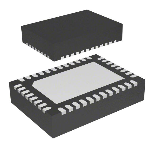


 工商网监
湘ICP备2023018690号
工商网监
湘ICP备2023018690号
