TPS546D24A
TPS546D24A
SLUSDN0A – DECEMBER 2019 – REVISED NOVEMBER
2020
SLUSDN0A – DECEMBER 2019 – REVISED NOVEMBER 2020
www.ti.com
TPS546D24A 2.95-V to 16-V, 40-A, Up to 4× Stackable, PMBus® Buck Converter
1 Features
3 Description
•
The TPS546D24A is a highly integrated, non-isolated
DC/DC converter capable of high frequency operation
and 40-A current output from a 7-mm × 5-mm
package. Two, three, and four TPS546D24A devices
can be interconnected to provide up to 160 A on a
single output. The device has an option to overdrive
the internal 5-V LDO with an external 5-V supply via
the VDD5 pin to improve efficiency and reduce power
dissipation of the converter.
•
•
•
•
•
•
•
•
•
•
•
•
•
•
Split rail support: 2.95-V to 16-V PVIN; 2.95-V to
18-V AVIN (4-VIN VDD5 for switching)
Integrated 4.5-mΩ/0.9-mΩ MOSFETs
Average current mode control with selectable
internal compensation
2×, 3×, 4× stackable with current sharing up to 160
A, supporting a single address per output
Selectable 0.5-V to 5.5-V output via pin strap or
0.25-V to 5.5-V using PMBus VOUT_COMMAND
Extensive PMBus command set with telemetry for
VOUT, IOUT and internal die temperature
Differential remote sensing with internal FB divider
for < 1% VOUT error –40°C to +150°C TJ
AVS and margining capabilities through PMBus
MSEL pins pin programming PMBus defaults
12 Selectable switching frequencies from 225 kHz
to 1.5 MHz (8 pin-strap options)
Frequency sync in/sync out
Supports prebiased output
Supports strongly coupled inductor
7-mm × 5-mm × 1.5-mm, 40-pin QFN,
pitch = 0.5 mm
Create a Custom Design Using the TPS546D24A
With WEBENCH® Power Designer
The TPS546D24A uses a proprietary fixed-frequency
current-mode control with input feedforward and
selectable internal compensation components for
minimal size and stability over a wide range of output
capacitances.
The PMBus interface with 1-MHz clock support gives
a convenient, standardized digital interface for
converter configuration as well as monitoring of key
parameters including output voltage, output current,
and internal die temperature. Response to fault
conditions can be set to restart, latch off, or ignore,
depending on system requirements. Back-channel
communication between stacked devices enables all
TPS546D24A converters powering a single output rail
to share a single address to simplify system software/
firmware design. Key parameters including output
voltage, switching frequency, soft-start time, and
overcurrent fault limits can also be configured through
BOM selection without PMBus communication to
support program free power-up.
2 Applications
•
•
•
•
Data center switches, rack servers
Active antenna system, remote radio and
baseband unit
Automated test equipment, CT, PET, and MRI
ASIC, SoC, FPGA, DSP core, and I/O voltage
Device Information
PART NUMBER (1)
TPS546D24A
(1)
PACKAGE
BODY SIZE (NOM)
LQFN-CLIP (40)
7.00 mm × 5.00 mm
For all available packages, see the orderable addendum at
the end of the data sheet.
DRTN
MSEL1
PVIN
AVIN
BP1V5
EN/UVLO
PGD/RST_B
VIN
VOSNS
GOSNS/SLAVE
BOOT
TPS546D24A
MSEL2
To Loop Slaves
SMB_ALRT
PMB_CLK
PMB_DATA
BCX_DAT
BCX_CLK
VDD5
SYNC
AGND
VSHARE
ADRSEL
VSEL
VOUT
SW
PGND
To PMBus
Simplified Application
An©IMPORTANT
NOTICEIncorporated
at the end of this data sheet addresses availability, warranty, changes, use in
safety-critical
applications,
Copyright
2020 Texas Instruments
Submit
Document
Feedback
intellectual property matters and other important disclaimers. PRODUCTION DATA.
Product Folder Links: TPS546D24A
1
�TPS546D24A
www.ti.com
SLUSDN0A – DECEMBER 2019 – REVISED NOVEMBER 2020
Table of Contents
1 Features............................................................................1
2 Applications..................................................................... 1
3 Description.......................................................................1
4 Revision History.............................................................. 2
5 Pin Configuration and Functions...................................3
6 Specifications.................................................................. 6
6.1 Absolute Maximum Ratings ....................................... 6
6.2 ESD Ratings .............................................................. 6
6.3 Recommended Operating Conditions ........................6
6.4 Thermal Information ...................................................6
6.5 Electrical Characteristics ............................................7
6.6 Typical Characteristics.............................................. 15
7 Detailed Description......................................................19
7.1 Overview................................................................... 19
7.2 Functional Block Diagram......................................... 19
7.3 Feature Description...................................................20
7.4 Device Functional Modes..........................................34
7.5 Programming............................................................ 36
7.6 Register Maps...........................................................47
8 Application and Implementation................................ 149
8.1 Application Information........................................... 149
8.2 Typical Application.................................................. 149
8.3 Two-Phase Application........................................... 159
8.4 Four-Phase Application...........................................164
9 Power Supply Recommendations..............................165
10 Layout.........................................................................166
10.1 Layout Guidelines................................................. 166
10.2 Layout Example.................................................... 167
10.3 Mounting and Thermal Profile Recommendation..167
11 Device and Documentation Support........................169
11.1 Device Support......................................................169
11.2 Receiving Notification of Documentation Updates 169
11.3 Support Resources............................................... 169
11.4 Trademarks........................................................... 169
11.5 Electrostatic Discharge Caution............................ 170
11.6 Glossary................................................................ 170
12 Mechanical, Packaging, and Orderable
Information.................................................................. 171
4 Revision History
NOTE: Page numbers for previous revisions may differ from page numbers in the current version.
Changes from Revision * (December 2019) to Revision A (November 2020)
Page
• Updated the numbering format for tables, figures and cross-references throughout the document. .................1
2
Submit Document Feedback
Copyright © 2020 Texas Instruments Incorporated
Product Folder Links: TPS546D24A
�TPS546D24A
www.ti.com
SLUSDN0A – DECEMBER 2019 – REVISED NOVEMBER 2020
5 Pin Configuration and Functions
Figure 5-1. 40-Pin LQFN-CLIP With Exposed Thermal Pad RVF Package (Top View)
Table 5-1. Pin Functions
PIN
NO.
NAME
I/O
DESCRIPTION
1
PGD/RST_B
I/O
Open-drain power good or (21h) VOUT_COMMAND RESET#. As determined by user-programmable
RESET# bit in (EDh) MFR_SPECIFIC_29 (MISC_OPTIONS). The default pin function is an open-drain
power-good indicator. When configured as RESET#, an internal pullup can be enabled or disabled by the
PULLUP# bit in (EDh) MFR_SPECIFIC_29 (MISC_OPTIONS).
2
PMB_DATA
I/O
PMBus DATA pin. See Current PMBus Specifications.
3
PMB_CLK
I
PMBus CLK pin. See Current PMBus Specifications.
4
BP1V5
O
Output of the 1.5-V internal regulator. This regulator powers the digital circuitry and should be bypassed
with a minimum of 1 µF to DRTN with an X5R or better ceramic capacitor rated for a minimum of 6 V.
BP1V5 is not designed to power external circuit.
5
DRTN
—
Digital bypass return for bypass capacitor for BP1V5. Internally connected to AGND. Do not connect to
PGND or AGND.
6
SMB_ALRT
O
SMBus alert pin. See SMBus specification.
Submit Document Feedback
Copyright © 2020 Texas Instruments Incorporated
Product Folder Links: TPS546D24A
3
�TPS546D24A
www.ti.com
SLUSDN0A – DECEMBER 2019 – REVISED NOVEMBER 2020
Table 5-1. Pin Functions (continued)
PIN
I/O
DESCRIPTION
BOOT
I
Bootstrap pin for the internal flying high side driver. Connect a typical 100-nF X5R or better ceramic
capacitor rated for a minimum of 10 V from this pin to SW. To reduce the voltage spike at SW, an optional
BOOT resistor of up to 8 Ω can be placed in series with the BOOT capacitor to slow down turn-on of the
high-side FET.
SW
I/O
Switched power output of the device. Connect the output averaging filter and bootstrap to this group of
pins.
PGND
—
Power stage ground return. These pins are internally connected to the thermal pad.
NO.
NAME
7
8
9
10
11
12
13
14
15
16
17
18
19
20
21
I
Input power to the power stage. Low-impedance bypassing of these pins to PGND is critical. PVIN to
PGND should be bypassed with X5R or better ceramic capacitors rated for at least 1.5x the maximum
PVIN voltage. In addition, a minimum of one 0402 2.2-nF - 10-nF X7R or better ceramic capacitance
rated for at least 1.5x the maximum PVIN voltage should placed as close to the PVIN and PGND pins or
under the PVIN pins to reduce the high-frequency bypass impedance.
22
23
PVIN
24
25
26
AVIN
I
Input power to the controller. Bypass with a minimum 1-µF X5R or better ceramic capacitor rated for at
least 1.5x the maximum AVIN voltage to AGND. If AVIN is connected to the same input as PVIN or
VDD5, a minimum 10-µs R-C filter between PVIN or VDD5 and AVIN is recommended to reduce
switching noise on AVIN.
27
EN/UVLO
I
Enable switching as the PMBus CONTROL pin. EN/UVLO can also be connected to a resistor divider to
program input voltage UVLO.
28
VDD5
O
Output of the 5-V internal regulator. This regulator powers the driver stage of the controller and should be
bypassed with a minimum of 4.7-µF X5R or better ceramic capacitor rated for a minimum of 10 V to
PGND at the thermal pad. Low impedance bypassing of this pin to PGND is critical.
29
MSEL2
I
Connect this pin to a resistor divider between BP1V5 and AGND for different options of soft-start time,
overcurrent fault limit,and multiphase information. See Programming MSEL2 or Programming MSEL2 for
a Slave Device (GOSNS Tied to BP1V5) for a Slave Device (GOSNS tied to BP1V5) if GOSNS is tied to
BP1V5.
30
VSEL
I
Connect this pin to a resistor divider between BP1V5 and AGND for different options of internal voltage
feedback divider and default output voltage. See Programming VSEL.
31
ADRSEL
I
Connect this pin to a resistor divider between BP1V5 and AGND for different options of PMBus
addresses and frequency sync (including determination of SYNC pin as SYNCIN or SYNCOUT
function).See Programming ADRSEL.
32
MSEL1
I
Connect this pin to a resistor divider between BP1V5and AGND for different options of switching
frequency and internal compensation parameters. See Programming MSEL1.
I
The positive input of the remote sense amplifier. For a stand-alone device or the loop master device in a
multi-phase configuration, connect VOSNS pin to the output voltage at the load. For the loop slave
device in a multi-phase configuration, the remote sense amplifier is not required for output voltage
sensing or regulation and this pin can be left floating. If used to monitor another voltage with the Phased
READ_VOUT command, VOSNS should be maintained between 0 V and 0.75 V with a 4.5 V, input current to PMB_DATA,
SMB_ALRT, BCX_DAT = 20 mA
0.4
V
IOH(PMBUS)
Output high level open drain
leakage current into
PMB_DATA, SMB_ALRT
Voltage on PMB_DATA, SMB_ALRT = 5.5 V
10
μA
IOL(PMBUS)
Output low level open drain
sinking current on
PMB_DATA, SMB_ALRT,
BCX_DAT
Voltage on PMB_DATA, SMB_ALRT, BCX_DAT =
0.4 V
20
fPMBUS_CLK
PMBus operating frequency
range
GOSNS = AGND
10
CPMBUS
PMBUS_CLK &
PMBUS_DATA pin input
capactiance(1)
Vpin = 0.1V to 1.35V
NWR_NVM
Number of NVM writeable
cycles(1)
–40°C to 150°C
tCLK_STCH(max)
Maximum Allowable Clock
Stretch(1)
(1)
(2)
(3)
(4)
(5)
14
1.35
V
0.8
mA
1000
kHz
5
pF
1000
cycle
6
ms
Specified by design. Not production tested.
The parameter covers 2.95 V to 18 V of AVIN.
The setting of TON_RISE and TOFF_FALL of 0 ms means the unit to bring its output voltage to the programmed regulation value of
down to 0 as quickly as possible, which results in an effective TON_RISE and TOFF_FALL time of 0.5 ms (fastest time supported).
The setting of TON_MAX_FAULT_LIMIT and TOFF_MAX_WARN_LIMIT of 0 means disabling TON_MAX_FAULT and
TOFF_MAX_WARN response and reporting completely.
Not production tested. Guaranteed by correlation. AVIN = PVIN = 12 V, VOUT = 1 V fsw = 325kHz L = 320nH
Submit Document Feedback
Copyright © 2020 Texas Instruments Incorporated
Product Folder Links: TPS546D24A
�TPS546D24A
www.ti.com
SLUSDN0A – DECEMBER 2019 – REVISED NOVEMBER 2020
6.6 Typical Characteristics
105
105
100
100
95
95
Ambient Temperature (qC)
Ambient Temperature (qC)
V PIN = V AVIN = 12 V, T A = 25°C, f sw = 325 kHz (unless otherwise specified). Safe operating area curves were
measured using a Texas Instruments evaluation module (EVM).
90
85
80
75
70
65
60
55
50
10
Nat conv
100 LFM
200 LFM
400 LFM
15
20
90
85
80
75
70
65
60
55
25
30
35
Phase Current (A)
40
45
50
10
50
Nat conv
100 LFM
200 LFM
400 LFM
15
20
D001
25
30
35
Phase Current (A)
40
45
50
D002
VIN = 5 V
VOUT = 1 V
Snubber = 1 nF + 1 Ω
VIN = 5 V
VOUT = 1 V
Snubber = 1 nF + 1 Ω
fSW = 325 kHz
L = 300 nH
RBOOT = 0 Ω
fSW = 550 kHz
L = 300 nH
RBOOT = 0 Ω
Figure 6-2. TPS546D24A Safe Operating Area
105
105
100
100
95
95
Ambient Temperature (qC)
Ambient Temperature (qC)
Figure 6-1. TPS546D24A Safe Operating Area
90
85
80
75
70
65
60
55
50
10
Nat conv
100 LFM
200 LFM
400 LFM
15
20
90
85
80
75
70
65
60
55
25
30
35
Phase Current (A)
40
45
50
10
50
Nat conv
100 LFM
200 LFM
400 LFM
15
20
D003
25
30
35
Phase Current (A)
40
45
50
D004
VIN = 12 V
VOUT = 1 V
Snubber = 1 nF + 1Ω
VIN = 12 V
VOUT = 1 V
Snubber = 1 nF + 1 Ω
fSW = 325 kHz
L = 300 nH
RBOOT = 0 Ω
fSW = 550 kHz
L = 300 nH
RBOOT = 0 Ω
105
100
95
90
85
80
75
70
65
60
55
50
45
40
35
10
Nat conv
100 LFM
200 LFM
400 LFM
15
20
Figure 6-4. TPS546D24A Safe Operating Area
Ambient Temperature (qC)
Ambient Temperature (qC)
Figure 6-3. TPS546D24A Safe Operating Area
25
30
35
Phase Current (A)
40
45
50
105
100
95
90
85
80
75
70
65
60
55
50
45
40
35
10
D005
Nat conv
100 LFM
200 LFM
400 LFM
15
20
25
30
35
Phase Current (A)
40
45
50
D006
VIN = 12 V
VOUT = 3.3 V
Snubber = 1 nF + 1Ω
VIN = 12 V
VOUT = 3.3 V
Snubber = 1 nF + 1 Ω
fSW = 325 kHz
L = 300nH
RBOOT = 0 Ω
fSW = 550 kHz
L = 300 nH
RBOOT = 0 Ω
Figure 6-5. TPS546D24A Safe Operating Area
Figure 6-6. TPS546D24A Safe Operating Area
Submit Document Feedback
Copyright © 2020 Texas Instruments Incorporated
Product Folder Links: TPS546D24A
15
�TPS546D24A
www.ti.com
110
110
100
100
Ambient Temperature (qC)
Ambient Temperature (qC)
SLUSDN0A – DECEMBER 2019 – REVISED NOVEMBER 2020
90
80
70
60
50
Nat conv
100 LFM
200 LFM
400 LFM
40
30
10
15
20
80
70
60
50
Nat conv
100 LFM
200 LFM
400 LFM
40
30
25
30
35
Phase Current (A)
40
45
20
10
50
15
20
D007
25
30
35
Phase Current (A)
40
45
50
D008
VIN = 12 V
VOUT = 5 V
Snubber = 1 nF + 1 Ω
VIN = 12 V
VOUT = 5 V
Snubber = 1 nF + 1 Ω
fSW = 325 kHz
L = 300 nH
RBOOT = 0 Ω
fSW = 550 kHz
L = 300 nH
RBOOT = 0 Ω
Figure 6-8. TPS546D24A Safe Operating Area
100
100
95
95
90
90
Efficiency (%)
Efficiency (%)
Figure 6-7. TPS546D24A Safe Operating Area
85
80
75
70
85
80
75
70
0.8V
1.0V
1.2V
3.3V
65
0.8V
1.0V
1.2V
3.3V
65
60
60
0
5
10
15
20
25
Load Current (A)
30
35
40
0
5
10
D009
15
20
25
Load Current (A)
30
35
40
D010
VIN = 5 V
L = 300 nH
Snubber = 1 nF + 1 Ω
VIN = 5 V
L = 300 nH
Snubber = 1 nF + 1 Ω
fSW = 325 kHz
RDCR = 0.15 mΩ
RBOOT = 0 Ω
fSW = 550 kHz
RDCR = 0.15 mΩ
RBOOT = 0 Ω
Figure 6-10. TPS546D24A Efficiency vs Output
Current
100
100
95
95
90
90
Efficiency (%)
Efficiency (%)
Figure 6-9. TPS546D24A Efficiency vs Output
Current
85
80
75
0.8V
1.0V
1.2V
3.3V
5.0V
70
65
85
80
75
0.8V
1.0V
1.2V
3.3V
5.0V
70
65
60
60
0
5
10
15
20
25
Load Current (A)
30
35
40
0
D011
VIN = 12 V
L = 300 nH
Snubber = 1 nF + 1 Ω
fSW = 325 kHz
RDCR = 0.15 mΩ
RBOOT = 0 Ω
Figure 6-11. TPS546D24A Efficiency vs Output
Current
16
90
5
10
15
20
25
Load Current (A)
30
35
40
D012
VIN = 12 V
L = 300 nH
Snubber = 1 nF + 1
Ω
fSW = 550 kHz
RDCR = 0.15 mΩ
RBOOT = 0 Ω
Figure 6-12. TPS546D24A Efficiency vs Output
Current
Submit Document Feedback
Copyright © 2020 Texas Instruments Incorporated
Product Folder Links: TPS546D24A
�TPS546D24A
www.ti.com
SLUSDN0A – DECEMBER 2019 – REVISED NOVEMBER 2020
9
1.65
8.5
1.55
8
7.5
Rdson (m:)
Rdson (m:)
1.45
1.35
1.25
1.15
6
5.5
1.05
5
Vgate
3.0V
4.5V
0.95
0.85
-40
7
6.5
-20
0
20
40
60
80 100
Temperature (qC)
120
140
Vgate = 3.0V
Vgate = 4.5V
4.5
4
-40
160
-20
0
20
D013
Figure 6-13. Low-Side MOSFET On-Resistance (R
DS(on))
vs Junction Temperature
40
60
80 100
Temperature (qC)
120
140
160
D014
Figure 6-14. High-Side MOSFET On-Resistance (R
DS(on))
vs Junction Temperature
1.003
700
650
Switching Frequency (kHz)
VOSNS - GOSNS (V)
1.002
1.001
1
0.999
0.998
-20
0
20
40
60
80 100
Temperature (qC)
120
140
550
500
450
400
350
300
325kHz
550kHz
250
VOUT = 1.00V
0.997
-40
600
200
-40
160
-20
0
20
D015
40
60
80 100
Temperature (qC)
120
140
160
D016
VOUT_COMMAND = 1 V
Figure 6-15. Output Voltage vs Junction
Temperature
Figure 6-16. Switching Frequency
vs Junction Temperature
4.75
13.8
13.6
13.4
4.725
13
VDD5 (V)
IAVIN (mA)
13.2
12.8
12.6
4.7
12.4
4.675
12.2
12
11.8
-40
-20
0
20
40
60
80 100
Temperature (qC)
120
140
160
4.65
-40
D017
IVDD5 = 10 mA
Figure 6-17. Non-Switching Input Current (IAVIN)
vs Junction Temperature
-20
0
20
40
60
80 100
Temperature (qC)
120
140
160
D018
VPVIN = VAVIN= 12 V
Figure 6-18. VDD5 Voltage vs Junction
Temperature
Submit Document Feedback
Copyright © 2020 Texas Instruments Incorporated
Product Folder Links: TPS546D24A
17
�TPS546D24A
www.ti.com
SLUSDN0A – DECEMBER 2019 – REVISED NOVEMBER 2020
2.9
1.55
2.85
PVIN_ON (V)
BP1V5 (V)
1.525
1.5
2.8
2.75
2.7
1.475
2.65
1.45
-40
-20
0
20
40
60
80 100
Temperature (qC)
IBP1V5 = 2 mA
120
140
2.6
-40
160
-20
0
20
D023
VPVIN = VAVIN= 12 V
40
60
80 100
Temperature (qC)
120
140
160
D019
(35h) VIN_ON = 2.75 V
Figure 6-19. BP1V5 Voltage vs Junction
Temperature
Figure 6-20. Turnon Voltage vs Junction
Temperature
2.65
1.1
2.6
EN/UVLO (V)
PVIN_OFF (V)
1.05
2.55
2.5
2.45
1
0.95
2.4
2.35
-40
ON
OFF
-20
0
20
40
60
80 100
Temperature (qC)
120
140
160
0.9
-40
D020
-20
0
20
40
60
80 100
Temperature (qC)
120
140
160
D021
Figure 6-22. EN/UVLO Thresholds vs Junction
Temperature
(36h) VIN_OFF = 2.5 V
Figure 6-21. Turnoff Voltage vs Junction
Temperature
18
Submit Document Feedback
Copyright © 2020 Texas Instruments Incorporated
Product Folder Links: TPS546D24A
�TPS546D24A
www.ti.com
SLUSDN0A – DECEMBER 2019 – REVISED NOVEMBER 2020
7 Detailed Description
7.1 Overview
The TPS546D24A uses a fixed-frequency, proprietary current-mode control. The switching frequency can be
selected from pre-set values through pin-strapping and PMBus programming. The output voltage is sensed
through a true differential remote sense amplifier and internal resistor divider, then compared to an internal
voltage reference by an error amplifier. An internal oscillator initiates the turnon of the high-side power switch.
The error amplifier output is buffered and shared through VSHARE among stacked devices. This shared voltage
is compared to the sensed switch node current to drive a linear voltage ramp modulator with input voltage,
output voltage, and switching frequency feedforward to regulate the average switch-node current. As a
synchronous buck converter, the device normally works in continuous conduction mode (CCM) under all load
conditions. The compensation components are integrated into the TPS546D24A devices, and programmable
through the PMBus command (B1h) USER_DATA_01 (COMPENSATION_CONFIG) or with the external pin
MSEL1 to select pre-set values based on switching frequency and output LC filters.
7.2 Functional Block Diagram
SYNC
MSEL2
BP1V5
VDD5
EN/UVLO
Auto-detection/
Decoder
PMBus
(SS, OC, Phase
SYNC
Count)
_IN
SYNC_
OUT
AVIN PVIN
Linear
Regulators
UVLO
PLL
To
Infrastructure
BOOT
BP1V8
Oscillator
PVIN
MSEL1
PWM
Decoder
(Fsw, Comp)
On-Time
Generator
MSEL2/PMBus
Driver
Control
SW
Anti-CrossConduction
VDD5
Pre-Bias
VSEL
Decoder
(Vref, Divider
Ratio)
Soft-Start
DAC
PGND
Output Current
Sensing
AGND
IMON
To Infrastructure &
Selectable Divider Ratio
R1
VOSNS
VSHARE
Error Amplifier with
Internal Compensation
+
Fault
Management
VOUT/UV/OV VMON & OV/UV
Detection
R2
GOSNS/SLAVE
RESET Vout
Slave
Detection
ADC, PMBus Interface, Back Channel
Interface, Memory
Decoder
(Addr, PH Pos,
Det SYNC in/out)
PGD/RST_B
TMON
Die Temp
Sensing
SMB_ALRT
BCX_DAT
PMB_CLK
DRTN
ADRSEL
PMB_DATA
BCX_CLK
Submit Document Feedback
Copyright © 2020 Texas Instruments Incorporated
Product Folder Links: TPS546D24A
19
�TPS546D24A
www.ti.com
SLUSDN0A – DECEMBER 2019 – REVISED NOVEMBER 2020
7.3 Feature Description
7.3.1 Average Current-Mode Control
The TPS546D24A device uses an average current-mode control architecture with independently programmable
current error integration and voltage error integration loops. This architecture provides similar performance to
peak current-mode control without restricting the minimum on-time or minimum-off time control, allowing the gain
selection of the current loop to effectively set the slope compensation. For help selecting compensation values,
customers can use the TPS546x24A Compensation and Pin-Strap Resistor Calculator design tool.
Voltage Feed Forward and Frequency Setting
Voltage Feed Forward
Switching Frequency
Remote Sense with Internal
Resistor Divider
Voltage Regulation Error Amplifier w/
Internal Type-II Compensator
VO_SNS
Unity Gain
Remote
Sense Amp
Voltage Error
Amp
Sensed
GMV
VOUT
+
-
g VOUT err
+
VREF
GND_SNS
+
High-Bandwidth
Average Current Mode
Control Amplifier w/
Internal Compensation
Icntrl
+
GMI
g IL err
-
RVV
I_SNS
CZV
CPV
RVI
Current Error
Amp
CZI
S
Q
R
Q
PWM
Vcntrl
TON
Generator
CPI
Start
High-Frequency, Low Jitter
On-Time Modulator
Common Internal Ground for Regulation
PLL Synchronizable
PWM_CLK_EDGE
VSHARE
Regulation & Current Share Loop for
Stackability
Figure 7-1. Average Current Mode Control Block Diagram
7.3.1.1 On-Time Modulator
The input voltage feedforward modulator converts the integrated current error signal, ILerr, into an inductor ontime that provides a controlled volt-second balance across the inductor over each full switching period that
simplifies the current error integration loop design. The modulator produces a full-cycle averaged small signal
Vcntrl to dIL/dt transfer function given by Equation 1:
dIL
dt
dVcntrl
VIN
1
u
Vramp L
5.5
L
(1)
Thus the inductor current modulator gain is given by Equation 2:
dIL
¦
dVcntrl
VIN
1
u
Vramp L u ¦
5.5
Lu¦
(2)
This natural integration 1/f function allows the current loop to be compensated by the mid-band gain of the error
current integrator.
20
Submit Document Feedback
Copyright © 2020 Texas Instruments Incorporated
Product Folder Links: TPS546D24A
�TPS546D24A
www.ti.com
SLUSDN0A – DECEMBER 2019 – REVISED NOVEMBER 2020
7.3.1.2 Current Error Integrator
The current error integrator adjusts the modulator control voltage to match the sensed inductor current, Isns, to
the current voltage at the VSHARE pin. The integrator is tuned through the GMI, RVI, CZI, CPI, and CZI_MUL
parameters in (B1h) USER_DATA_01 (COMPENSATION_CONFIG). Thanks to the natural integration of the 1/f
function of the current control gain, the bandwidth of the current control loop can be adjusted with the mid-band
gain of the integrator, GMI × RVI.
The current loop crossover occurs at the frequency when the full loop gain is equal to 1 according to Equation 3:
ILOOP ¦ u
VPVIN
1
u CSA u
Vramp
1.7 u S u ¦ u /
1
(3)
Solving for the mid-band gain of the current loop, you find Equation 4:
ILOOPMB
GMI u RVI
Vramp
u
VPVIN
1.7
u L u S u ¦coi
CSA
(4)
While Nyquist Theorem suggests that a bandwidth of ½ fSW is possible, inductor tolerances and phase delays in
the current sense, modulator, and H-bridge power FETs make f SW/4 a more practical target, which simplifies the
target current loop midband gain to achieve a current loop bandwidth of fSW/4 to Equation 5:
ILOOPMB
GMI u RVI
Vramp
u
VPVIN
¦
1.7
u L u S u sw
CSA
4
1.7 u S
4 u 5.5 u 6.155 u 10
3
u / u ¦sw
u / u ¦sw
(5)
An integrator from DC to the low-frequency zero, RVI × CZI, compensates for the valley voltage of the modulator
ramp and the nominal offset of the output voltage. A high-frequency filter pole, RVI × CPI between half the
switching frequency and the switching frequency reduces high-frequency noise from VSHARE and minimizes
pulse-width jitter.
To avoid loop interactions, the integrating zero frequency should be below the voltage loop cross-over frequency,
while the high-frequency pole should be between ½ the switching frequency and the switching frequency to limit
high-frequency noise and jitter in the current loop without imposing additional phase loss in the voltage loop.
The closed loop average current mode control allows the current sense amplifier, on-time modulator, H-bridge
power FETs, and inductor to operate as a transconductance amplifier with forward gain of 1/CSA or 162.5 A/V
with a bandwidth equal to Fcoi.
7.3.1.3 Voltage Error Integrator
The voltage error integrator regulates the output voltage by adjusting the current control voltage, VSHARE,
similar to any current mode control architecture. A transconductance amplifier compares the sense feedback
voltage to a programmed reference voltage to set the current control voltage VSHARE to maintain the desired
output voltage. While a regulated current source feeding an output capacitance provides a natural, stable
integrator, mid-band gain is often desired to improve the loop bandwidth and transient response.
With a transconductance set by the current sense gain, the voltage loop cross-over occurs when the full loop
gain equal 1 according to Equation 6.
VOUT _ SCALE _ LOOP u VLOOP ¦ u
1
u ZOUT ¦
CSA
1
(6)
To prevent the current integration loop bandwdith from negatively impacting the phase margin of the voltage
loop, the voltage loop should have a target bandwidth of Fcoi / 2.5. With a current mode loop of f SW/4, the
voltage loop mid-band gain should be Equation 7:
Submit Document Feedback
Copyright © 2020 Texas Instruments Incorporated
Product Folder Links: TPS546D24A
21
�TPS546D24A
www.ti.com
SLUSDN0A – DECEMBER 2019 – REVISED NOVEMBER 2020
VLOOPMB
GMV u RVV
1
u
VOUT _ SCALE _ LOOP
CSA
·
§f
ZOUT ¨ SW ¸
© 10 ¹
(7)
An integrator pole is necessary to maintain accurate DC regulation, and the zero-frequency set by RVV × CZV
should be set below the lowest cross-over frequency with the largest output capacitor intended to be supported
at the output, but not more than 1/2 the target voltage loop crossover frequency fcov.
A high frequency noise pole, intended to keep switching noise out of the current loop should also be employed,
with a high-frequency pole set by RVV × CPV should be set between fsw/4 and fsw.
For pin programmed options of compensation components, see Table 7-9.
For PMBus programming of compensation values, see (B1h) USER_DATA_01 (COMPENSATION_CONFIG).
7.3.2 Linear Regulators
The TPS546D24A devices have three internal linear regulators receiving power from AVIN and providing
suitable bias (1.5 V, 1.8 V, and 5 V) for the internal circuitry of the device. External bypass pins for VDD5 and
BP1V5 must be bypassed to their respective grounds for the converter to function properly. BP1V5 requires a
minimum of 1 μF of capacitance connected to DRTN. VDD5 requires a minimum 4.7 μF of capacitance
connected to PGND. Once AVIN, 1.5-V, 1.8-V, and 5-V reach their respective UVLOs, the device initiates a
power-on reset, after which the device can be communicated with through PMBus for configuration and users
can store defaults to the NVM.
The VDD5 has internally-fixed undervoltage lockout of 3.9 V (typ.) to enable power-stage conversion. The VDD5
regulator can also be fed by external supply to reduce internal power dissipation and improve efficiency by
eliminating the loss in the internal LDO, or to allow operation with AVIN less than 4 V. The external supply should
be higher voltage than the LDO regulation voltage programmed by (B5h) USER_DATA_05
(POWER_STAGE_CONFIG).
Place bypass capacitors as close as possible to the device pins, with a minimum return loop back to their
respective ground. Keep the return loop away from fast switching voltage and main current path — see Layout
for details. Poor bypassing can degrade the performance of the regulator.
The use of the internal regulators to power other circuits is not recommended because the loads placed on the
regulators might adversely affect operation of the controller.
7.3.3 AVIN and PVIN Pins
The device allows for a variety of applications by using the AVIN and PVIN pins together or separately. The AVIN
pin voltage supplies the internal control circuits of the device. The PVIN pin voltage provides the input voltage to
the switching power stage. When connected to a single supply, the input voltage for AVIN and PVIN can range
from 4 V to 16 V. If the PVIN is connected to separate supply from AVIN, the PVIN voltage can be 2.95 V to 16 V,
and AVIN has to meet 4-V minimum and 18-V maximum to drive the control and driver. If AVIN is connected to
the same supply as PVIN or VDD5, TI recommends a minimum 10-µs R-C filter with a 1-Ω to 10-Ω resistor and
AVIN bypass capacitor between AVIN and PVIN to reduce PVIN switching noise on the AVIN input.
22
Submit Document Feedback
Copyright © 2020 Texas Instruments Incorporated
Product Folder Links: TPS546D24A
�TPS546D24A
www.ti.com
SLUSDN0A – DECEMBER 2019 – REVISED NOVEMBER 2020
2.95 V ± 16 V
PVIN
VDD5
PGND
4.25 V ± 18 V
AVIN
AGND
Figure 7-2. TPS546D24A Separate PVIN and AVIN connections
2.95 V ± 16 V
PVIN
VDD5
PGND
4 V ± 5.25 V
AVIN
AGND
Figure 7-3. TPS546D24A Separate PVIN and AVIN connections with VDD5
Submit Document Feedback
Copyright © 2020 Texas Instruments Incorporated
Product Folder Links: TPS546D24A
23
�TPS546D24A
www.ti.com
SLUSDN0A – DECEMBER 2019 – REVISED NOVEMBER 2020
2.95 V ± 16 V
4.75 V ± 5.25 V
PVIN
VDD5
PGND
2.95 V ± 18 V
or PVIN
AVIN
AGND
Figure 7-4. TPS546D24A Separate PVIN, AVIN, and VDD5 Connections
7.3.4 Input Undervoltage Lockout (UVLO)
The TPS546D24A provides four independent UVLO functions for the broadest range of flexibility in start-up
control. While only the fixed AVIN UVLO is required to enable PMBus connectivity as well as VOUT and
TEMPERATURE monitoring, all four UVLO functions must be met before switching can be enabled.
7.3.4.1 Fixed AVIN UVLO
The TPS546D24A has internally fixed UVLO of 2.5 V (typical) on AVIN to enable the digital core and initiate
power on reset, including pin detection. The off-threshold on AVIN is 2.3 V (typ).
7.3.4.2 Fixed VDD5 UVLO
The TPS546D24A has an internally-fixed UVLO of 3.9 V (typ) on VDD5 to enable drivers and output voltage
conversion. The off-threshold on VDD5 is 3.5 V.
7.3.4.3 Programmable PVIN UVLO
Two PMBus commands ((35h) VIN_ON and (36h) VIN_OFF) allow the user to set PVIN voltage turnon and
turnoff thresholds independently, with 0.25-V resolution from 2.75 V to 15.75 V (6-bit) for (35h) VIN_ON and from
2.5 V to 15.5 V (6-bit) for (36h) VIN_OFF.
Note
If (36h) VIN_OFF is programmed higher than (35h) VIN_ON, the TPS546D24A rapidly switches
between enabled and disabled while PVIN remains below (36h) VIN_OFF. Propagation delays
between enable and disable can result in the converter starting (61h) TON_RISE and (65h)
TOFF_FALL in such conditions.
7.3.4.4 EN/UVLO Pin
The TPS546D24A also offers a precise threshold and hysteresis current source on the EN/UVLO pin so that it
can be used to program an additional UVLO to any external voltage greater than 1.05 V (typ.), including AVIN,
PVIN, or VDD5. For an added level of flexibility, the EN/UVLO pin can be disabled or its logic inverted through
the PMBUS Command (02h) ON_OFF_CONFIG, which allows the pin to be connected to AGND to ensure the
output is not enabled until PMBus programming has been completed.
24
Submit Document Feedback
Copyright © 2020 Texas Instruments Incorporated
Product Folder Links: TPS546D24A
�TPS546D24A
www.ti.com
SLUSDN0A – DECEMBER 2019 – REVISED NOVEMBER 2020
PVIN
Ihys
EN/UVLO
CNTRL
AGND
Figure 7-5. TPS546D24A UVLO Voltage Divider
7.3.5 Start-Up and Shutdown
The start-up and shutdown of the device is controlled by several PMBus programmable values including:
•
•
•
•
•
•
(01h) OPERATION
(02h) ON_OFF_CONFIG
(60h) TON_DELAY
(61h) TON_RISE
(64h) TOFF_DELAY
(65h) TOFF_FALL
With the default (02h) ON_OFF_CONFIG settings, the timing is as shown in Figure 7-6. See the Supported
PMBus Commands for full details on the implementation.
Submit Document Feedback
Copyright © 2020 Texas Instruments Incorporated
Product Folder Links: TPS546D24A
25
�TPS546D24A
www.ti.com
SLUSDN0A – DECEMBER 2019 – REVISED NOVEMBER 2020
CNTRL
VDD5_OK
PVIN_OK
VOUT
TON_DELAY
TON_RISE
TOFF_DELAY
TOFF_FALL
Figure 7-6. TPS546D24A Start-up and Shutdown
Note
The TPS546D24A requires time between the AVIN and VDD5 reaching their UVLO levels for pindetection and PMBus Communication and valid sensing of EN/UVLO and PVIN_OK. Once AVIN and
VDD5 exceed their lower UVLO thresholds (2.9-V typ.), the TPS546D24A starts its power-on-reset,
self-calibration, and pin-detection. This time delay, t delay(uvlo_PMBus) (6 ms typ.) must be complete
before PVIN_OK or EN/UVLO sensing is enabled.
If VDD5PS_ON, PVIN_OK, and EN/UVLO are above their thresholds before the end of tdelay(uvlo_PMBus),
(60h) TON_DELAY will start after tdelay(uvlo_PMBus) completes.
If VDD5 PS_ON, PVIN_OK, or EN/UVLO are below their thresholds when t delay(uvlo_PMBus) completes,
(60h) TON_DELAY will start when VDD5_OK, PVIN_OK, and EN/UVLO are all above their thresholds.
7.3.6 Differential Sense Amplifier and Feedback Divider
The TPS546D24A includes a fully integrated, internal, precision feedback divider and remote sense. Using both
the selectable feedback divider and precision adjustable reference, output voltages up to 6.0 V can be obtained.
The feedback divider can be programmed to divider ratios of 1:1, 1:2, 1:4, or 1:8 using the (29h)
VOUT_SCALE_LOOP command.
The recommended operating range of (21h) VOUT_COMMAND is dependent upon the feedback divider ratio
configured (29h) VOUT_SCALE_LOOP as follows:
Table 7-1. (29h) VOUT_SCALE_LOOP and (21h)
VOUT_COMMAND Recommended Range
RECOMMENDED VOUT
RANGE (V)
1
0.25 to 0.75
0.5
0.5 to 1.5
0.25
1 to 3
0.125
2 to 6
Setting (21h) VOUT_COMMAND lower than the recommended range can negatively affect VOUT regulation
accuracy while setting (21h) VOUT_COMMAND above the recommended range can limit the actual output
voltage achieved.
26
Submit Document Feedback
Copyright © 2020 Texas Instruments Incorporated
Product Folder Links: TPS546D24A
�TPS546D24A
www.ti.com
SLUSDN0A – DECEMBER 2019 – REVISED NOVEMBER 2020
Note
If the regulation output voltage is limited by the recommended range of the current (29h)
VOUT_SCALE_LOOP value, VOUT can be below the intended (43h) VOUT_UV_WARN_LIMIT or
(44h) VOUT_UV_FAULT_LIMIT without triggering their respective warning or faults due to the limited
range of the reference voltage.
7.3.7 Set Output Voltage and Adaptive Voltage Scaling (AVS)
The initial output voltage can be set by the VSEL pin at AVIN power up. As part of power-on reset (POR), the
VSEL pin senses both the resistance from the VSEL pin to AGND and the divider ratio of the VSEL pin between
B1V5 and AGND. These values program (29h) VOUT_SCALE_LOOP, (21h) VOUT_COMMAND, (2Bh)
VOUT_MIN, and (24h) VOUT_MAX and select the appropriate settings for the internal feedback divider and
precision adjustable reference voltage. Once the TPS546D24A completes its POR and enables PMBus
communication, these initial values can be changed through PMBus communication.
•
•
•
•
•
•
•
•
(20h) VOUT_MODE
(21h) VOUT_COMMAND
(29h) VOUT_SCALE_LOOP
(22h) VOUT_TRIM
(25h) VOUT_MARGIN_HIGH
(26h) VOUT_MARGIN_LOW
(01h) OPERATION
(02h) ON_OFF_CONFIG
The output voltage can be programmed through PMBus and its value is related to the following registers:
•
•
•
•
•
•
(24h) VOUT_MAX
(2Bh) VOUT_MIN
(40h) VOUT_OV_FAULT_LIMIT
(42h) VOUT_OV_WARN_LIMIT
(43h) VOUT_UV_WARN_LIMIT
(44h) VOUT_UV_FAULT_LIMIT
The TPS546D24A defaults to the relative format for the following, but can be changed to use absolute format
through the PMBus command (20h) VOUT_MODE:
•
•
•
•
•
•
(25h) VOUT_MARGIN_HIGH
(26h) VOUT_MARGIN_LOW
(40h) VOUT_OV_FAULT_LIMIT
(42h) VOUT_OV_WARN_LIMIT
(43h) VOUT_UV_WARN_LIMIT
(44h) VOUT_UV_FAULT_LIMIT
Refer to the detailed description of (20h) VOUT_MODE for details.
7.3.7.1 Reset Output Voltage
The (21h) VOUT_COMMAND value and the corresponding output voltage can be reset to the last selected
power-on reset value set by VSEL or EEPROM as selected in the (EEh) MFR_SPECIFIC_30
(PIN_DETECT_OVERRIDE) command when the PGD/RST_B pin function is set to RESET# in the (EDh)
MFR_SPECIFIC_29 (MISC_OPTIONS) PMBus command. To reset (21h) VOUT_COMMAND to its last PowerOn Reset value, when the RESET# optional function is enabled, assert the PGD/RST_B pin low externally.
While RESET# is asserted low, (21h) VOUT_COMMAND values received through PMBus is ACKed but no
change in (21h) VOUT_COMMAND is made. When RESET# is selected in (EDh) MFR_SPECIFIC_29
(MISC_OPTIONS), an internal pullup on the PGD/RST_B pin can be selected by the PULLUP# bit in the same
PMBus command to eliminate the need for an external pullup with the RESET# function.
Submit Document Feedback
Copyright © 2020 Texas Instruments Incorporated
Product Folder Links: TPS546D24A
27
�TPS546D24A
www.ti.com
SLUSDN0A – DECEMBER 2019 – REVISED NOVEMBER 2020
PGD/
RST_B
Boot VOUT (VSEL or NVM)
Pre-AVS VOUT
VOUT
Slew Rate set by
VOUT_TRANSITION_RATE
AVS by
VOUT_COMMAND
RST_B Response Delay
Figure 7-7. TPS546D24A Output Voltage Reset
7.3.7.2 Soft Start
To control the inrush current needed to charge the output capacitor bank during start-up, the TPS546D24A
implements a soft-start time programmed by the (61h) TON_RISE command. When the device is enabled, the
reference voltage ramps from 0 V to the final level defined by the following at a slew rate defined by the (61h)
TON_RISE command:
•
•
•
•
•
•
(21h) VOUT_COMMAND
(29h) VOUT_SCALE_LOOP
(22h) VOUT_TRIM
(25h) VOUT_MARGIN_HIGH
(26h) VOUT_MARGIN_LOW
(01h) OPERATION
The TPS546D24A devices support several soft-start times from 0 ms to 31.75 ms in 250-µs steps (7 bits)
selected by the (61h) TON_RISE command. The tON_RISE time is selectable by pin-strapping through the MSEL2
pin (eight options), PMBus programming, or both.
During soft start, when the PWM pulse width is shorter than the minimum controllable on-time, pulse skipping
can be seen and the output can show larger ripple voltage than normal operation.
7.3.8 Prebiased Output Start-Up
The TPS546D24A limits current from being discharged from a pre-biased output voltage during start-up by
preventing the low-side FET from forcing the SW node low until after the first PWM pulse turns on the high-side
FET. Once VOSNS voltage exceeds the increasing reference voltage and high-side SW pulses start, the
TPS546D24A limits the synchronous rectification during each SW period with a narrow on-time. The maximum
low-side MOSFET on-time slowly increases on a cycle-by-cycle basis until 128 switch periods have elapsed and
the synchronous rectifier runs fully complementary to the high-side MOSFET. This limits the sinking of current
from a pre-biased output, and ensures the output voltage start-up and ramp-to regulation sequences are
monotonically increasing.
In the event of a pre-biased output voltage greater than (40h) VOUT_OV_FAULT_LIMIT, the TPS546D24A
responds as soon as it completes POR and VDD5 is greater than its own 3.9-V UVLO, even if conversion is
disabled by EN/UVLO or the PMBus (01h) OPERATION command.
7.3.9 Soft Stop and (65h) TOFF_FALL Command
When enabled by (02h) ON_OFF_CONFIG or (01h) OPERATION, the TPS546D24A implements (65h)
TOFF_FALL command to force a controlled decrease of the output voltage from regulation to 0. There can be
negative inductor current forced during the (65h) TOFF_FALL time to discharge the output voltage. The setting
of (65h) TOFF_FALL of 0 ms means the unit to bring its output voltage down to 0 as quickly as possible, which
results in an effective (65h) TOFF_FALL time of 0.5 ms. When disabled in the (02h) ON_OFF_CONFIG for the
turnoff controlled by EN/UVLO pin or bit 6 of (01h) OPERATION if the regulator is turned off by (01h)
28
Submit Document Feedback
Copyright © 2020 Texas Instruments Incorporated
Product Folder Links: TPS546D24A
�TPS546D24A
www.ti.com
SLUSDN0A – DECEMBER 2019 – REVISED NOVEMBER 2020
OPERATION command, both high-side and low-side FET drivers are turned off immediately and the output
voltage slew rate is controlled by the discharge from the external load.
This feature is disabled for EN/UVLO in (02h) ON_OFF_CONFIG by default.
7.3.10 Power Good (PGOOD)
When conversion is enabled and t ON_RISE complete, if the output voltage remains between (43h)
VOUT_UV_WARN_LIMIT and (42h) VOUT_OV_WARN_LIMIT, the PGOOD open-drain output is released and
allowed to rise to an externally supplied logic level. Upon any fault condition with a shutdown response, the
PGOOD open-drain output is asserted, forcing PGOOD low by default. See Table 7-4 for the possible sources to
pull down the PGOOD pin.
The PGOOD signal can be connected to the EN/UVLO pin of another device to provide additional controlled
turnon and turnoff sequencing.
7.3.11 Set Switching Frequency
An internal oscillator generates a 225-kHz to 1.5-MHz clock for PWM switching with 16 discrete programmable
options. The switching frequency is selectable by pin-strapping through the resistor divider of MSEL1 (8 options),
PMBus programming (16 options), or both, using the (33h) FREQUENCY_SWITCH command, listed in Table
7-2.
Table 7-2. Oscillator fSW Options
AVAILABLE fSW OPTIONS (kHz)
fSW PIN-STRAPPING OPTIONS (kHz)
225
275
275
325
325
375
450
450
550
550
650
650
750
900
900
1100
1100
1300
1500
1500
7.3.12 Frequency Synchronization
The oscillator can be synchronized to external clock (SYNC IN) or output a clock to synchronize other devices
(SYNC out) on the SYNC pin. To support phase shifted clock for both multi-rail interleaving and multi-phase
operation, the internal oscillator can be phase-shifted from the SYNC pin by 0, 90, 120, 180, 240, or 270
degrees for 1, 2, 3, or 4 phase operation. The SYNC IN or SYNC OUT function, and phase position of single
phase or stand-alone devices can be selected by pin-strapping through resistor divider on at the ADRSEL pin, or
by the resistor from the MSEL2 pin to AGND for multi-phase slave devices.
In single output multi-phase stack configurations, the SYNC phase offset is programmed along with device count
and phase position using the MSEL2 pin. Slave devices in multi-phase stacks are always configured as
SYNC_IN while the master device can be configured for auto-detect, SYNC_IN, or SYNC_OUT through the
resistor divider on the ADRSEL pin.
Table 7-3. Pin Programmed Phase Positions through ADRSEL Resistor Divider (Single Phase StandAlone)
RDIV CODE
PHASE POSITION (DEGREE)
SYNC IN/OUT
Open (No resistor to BP1V5)
0
Auto-detect In/Out
0, 1
0
In
Submit Document Feedback
Copyright © 2020 Texas Instruments Incorporated
Product Folder Links: TPS546D24A
29
�TPS546D24A
www.ti.com
SLUSDN0A – DECEMBER 2019 – REVISED NOVEMBER 2020
Table 7-3. Pin Programmed Phase Positions through ADRSEL Resistor Divider (Single Phase StandAlone) (continued)
RDIV CODE
PHASE POSITION (DEGREE)
SYNC IN/OUT
2, 3
90
In
4, 5
120
In
6, 7
180
In
8, 9
240
In
10,11
270
In
12, 13
0
Out
14, 15
180
Out
After initial power up and pin detection, if SYNC IN/OUT is set as auto-detection configuration, the TPS546D24A
senses the SYNC pin to determine if there is any external SYNC clock. Switching or a consistent pullup on the
SYNC pin sets the device for SYNC_IN while a consistent pulldown on SYNC sets the device for SYNC_OUT.
The TPS546D24A devices programmed to be loop slaves are always programmed to be SYNC IN.
When configured for SYNC_IN, if SYNC input pulses are missed for two cycles, or the oscillator frequency drops
below 50% of the free-running switching frequency, the device determines that SYNC clock is lost. If the
TPS546D24A is part of a multi-phase stack, the converter shuts down and remains disabled until a SYNC signal
is reestablished to prevent damage due to the loss of synchronization. Single phase stand-alone devices
continues to operate at approximately 50% of the nominal frequency.
7.3.13 Loop Slave Detection
The GOSNS/SLAVE pin voltage is detected at power up. When it is pulled high to BP1V5, the device is
recognized as loop slave. When the GOSNS/SLAVE pin is connected to the Output Ground, the TPS546D24A is
configured as a loop master.
7.3.14 Current Sensing and Sharing
Both high-side and low-side FET use a SenseFET architecture for current sensing to achieve accurate and
temperature compensated current monitoring. This SenseFET architecture uses the parasitic resistance of the
FETs to achieve lossless current sense with no external components.
When multiple (2×, 3×, or 4×) devices operate in multi-phase application, all devices share the same internal
control voltage through VSHARE pin. The sensed current in each phase is regulated by the VSHARE voltage by
internal transconductance amplifier, to achieve loop compensation and current balancing between different
phases. The amplifier output voltage is compared with an internal PWM ramp to generate the PWM pulse.
7.3.15 Telemetry
The telemetry sub-system in the controller core supports direct measurements of input voltage, output voltage,
output current, and die temperature. The ADC supports internal rolling window averaging with rolling windows up
to 16 previous measurements for accurate measurements of these key system parameters. Each ADC
conversion requires less than 500 µs, allowing each telemetry value to be updated within 2 ms.
The current sense telemetry, which senses the low-side FET current at the start and end of each low-side FET
on-time and averages the two measurements to monitor the average inductor current over-report current if the
inductor current is non-linear during the low-side FET on-time, such as when the inductor is operating above its
saturation current.
7.3.16 Overcurrent Protection
Both low-side overcurrent (OC) and high-side short circuit protection are implemented.
The low-side overcurrent fault and warning thresholds are programmed through PMBus and sensed across
cycle-by-cycle average current through the low-side MOSFET and compared to the set warning or fault threshold
while High-side pulses are terminated on a cycle-by-cycle basis, if the peak current through the high-side
MOSFET exceeds the 1.5× the programmed low-side threshold.
30
Submit Document Feedback
Copyright © 2020 Texas Instruments Incorporated
Product Folder Links: TPS546D24A
�TPS546D24A
www.ti.com
SLUSDN0A – DECEMBER 2019 – REVISED NOVEMBER 2020
When either a low-side overcurrent or high-side short circuit threshold is exceeded during a switching cycle, an
OCP fault counter is incremented. If no overcurrent condition is detected in a switching cycle, the counter is
decremented. If the counter exceeds the delay selected by the (47h) IOUT_OC_FAULT_RESPONSE PMBus
value (default = 3) overcurrent fault condition is declared and the output shuts down. Restart and timing is also
defined as part of (47h) IOUT_OC_FAULT_RESPONSE.
The output OC fault thresholds and fault response are set through PMBUS. The OC fault response can be set to
shutdown, restart, or ignore.
7.3.17 Overvoltage/Undervoltage Protection
The voltage on VOSNS pin is monitored to provide output voltage overvoltage (OV) and undervoltage (UV)
protection. When VOSNS voltage is higher than OV fault threshold, OV fault is declared and the low-side FET is
turned on to discharge the output voltage and eliminate the OV condition. The low-side FET remains on until the
VOSNS voltage is discharged to 200 mV divide by the internal feedback divider as programmed by (29h)
VOUT_SCALE_LOOP. Once the output voltage is discharged, the output is disabled and the converter times out
and restarts according to the (41h) VOUT_OV_FAULT_RESPONSE PMBus command. When VOSNS voltage is
lower than UV fault threshold, UV fault is declared. After an initial delay programmed by the (45h)
VOUT_UV_FAULT_RESPONSE PMBus command, the output is disabled and the converter times out and
restarts according to the (45h) VOUT_UV_FAULT_RESPONSE PMBus command.
The output UV/OV fault thresholds and fault response are set through PMBUS. The UV/OV fault response can
be set to shutdown, restart, or continue operating without interruption.
7.3.18 Overtemperature Management
There are two schemes of overtemperature protections in the TPS546D24A device:
1. On-chip die temperature sensor for monitoring and overtemperature protection (OTP)
2. The bandgap based thermal shutdown (TSD) protection. TSD provides OT fail-safe protection in the event of
a failure of the temperature telemetry system, but can be disabled through (50h) OT_FAULT_RESPONSE for
high temperature testing
The overtemperature protection (OTP) threshold is set through PMBus and compares the (8Dh)
READ_TEMPERATURE_1 telemetry to the (51h) OT_WARN_LIMIT and (4Fh) OT_FAULT_LIMIT. The
overtemperature (OT) fault response can be set to shutdown, restart, or continue operating without interruption.
7.3.19 Fault Management
For the response on OC fault, OT fault, and thermal shutdown for multi-phase stack, the shutdown response has
the highest priority, followed by restart response. Continue operating without interruption response has the
lowest priority.
When multiple faults occur in rapid succession, it is possible for the first fault to occur to mask the second fault. If
the first fault to be detected is configured to continue operating without interruption, and the second fault is
configured to shutdown and restart, the second fault will shutdown but can fail to restart as programmed.
Table 7-4. Fault Protection Summary
FAULT OR
WARNING
Internal OT fault
Internal OT warning
FAULT RESPONSE
SETTING
FET BEHAVIOR
(4Fh)
OT_FAULT_LIMIT
Shutdown
Both FETs off
Restart
Both FETs off, restart
Ignore
FETS still controlled by PWM
(51h)
OT_WARN_LIMIT
Shutdown or restart
on Fault
FETS still controlled by PWM
PROGRAMMING
ACTIVE DURING t
ON_RISE
Yes
SMB_ALRT
MASKABLE
Y
Y
PGOOD LOGIC
Low
High
Yes
Y
Y
Yes
Y
Y
Yes
Y
Y
High
Ignore fault
TSD
Low Side OC fault
Threshold fixed
internally
(46h)
IOUT_OC_FAULT_LI
MIT
Shutdown
Both FETs off
Restart
Both FETs off, restart
Ignore
FETS still controlled by PWM
Shutdown
3 PWM counts, then both FETs off
Restart
3 PWM counts, then both FETs
off, restart after [DELAY]*tON_RISE
Ignore
FETS still controlled by PWM
Low
High
Low
High
Submit Document Feedback
Copyright © 2020 Texas Instruments Incorporated
Product Folder Links: TPS546D24A
31
�TPS546D24A
www.ti.com
SLUSDN0A – DECEMBER 2019 – REVISED NOVEMBER 2020
Table 7-4. Fault Protection Summary (continued)
FAULT OR
WARNING
Low Side OC
warning
PROGRAMMING
(4Ah)
IOUT_OC_WARN_LI
MIT
Negative OC fault
(lower priority than
OVF)
N/A
High side OC fault
(46h)
IOUT_OC_FAULT_LI
MIT
FAULT RESPONSE
SETTING
Shutdown or restart
on Fault
FET BEHAVIOR
MASKABLE
PGOOD LOGIC
Yes
Y
Y
High
Yes
Y
Y
Yes
Y
Y
Ignore fault
Enable
Turn off LS FET
Disable
FETS still controlled by PWM
Shutdown
3 cycles of pulse-by-pulse current
limiting followed by both FETs off
Restart
3 cycles of pulse-by-pulse current
limiting followed by both FETs off,
restart after [DELAY]*tON_RISE
Ignore
FETS still controlled by PWM
LS FET latched ON or turned on
till VOUTreaches 200mV/
VOUT_SCALE_LOOP; HS FET
OFF
Restart
LS FET latched ON or turned on
till VOUTreaches 200mV/
VOUT_SCALE_LOOP; HS FET
OFF, restart after [DELAY] * t
Ignore
FETS still controlled by PWM
Shutdown
LS FET latched ON or turned on
till VOUTreaches 200mV/
VOUT_SCALE_LOOP; HS FET
OFF
Restart
LS FET latched ON or turned on
till VOUTreaches 200mV/
VOUT_SCALE_LOOP; HS FET
OFF, restart after [DELAY]*t
Ignore
FETS still controlled by PWM
(42h)
VOUT_OV_WARN_L
IMIT
Shutdown or restart
on Fault
FETS still controlled by PWM
(44h)
VOUT_UV_FAULT_L
IMIT
Shutdown
Both FETs off
Restart
Both FETs off , restart after
[DELAY]*tON_RISE
Ignore
FETS still controlled by PWM
(43h)
VOUT_UV_WARN_L
IMIT
Shutdown or restart
on Fault
FETS still controlled by PWM
(62h)
TON_MAX_FAULT_L
IMIT
Shutdown
Both FETs off
Restart
Both FETs off, restart after
[DELAY]*tON_RISE
Ignore
FETS still controlled by PWM
PVin UVLO
(35h) VIN_ON, (36h)
VIN_OFF
Shutdown
Both FETs off
PVIN OV FAULT
(55h)
VIN_OV_FAULT_LIM
IT
Shutdown
Both FETs off
Restart
Both FETs off, restart
(40h)
VOUT_OV_FAULT_L
IMIT
SMB_ALRT
ON_RISE
FETS still controlled by PWM
Shutdown
Vout OV fault
ACTIVE DURING t
Low
High
Low
High
No
Y
Y
Low
ON_RISE
VOUT OVF fix
(40h)
VOUT_OV_FAULT_L
IMIT
High
Yes
Y
Y
Low
ON_RISE
Vout OV warning
Vout UV fault
Vout UV warning
tON MAX rault
High
No
Y
Y
No
Y
Y
High
Ignore Fault
Low
High
No
Y
Y
Yes
Y
Y
Low
Ignore fault
Ignore
FETS still controlled by PWM
BCX_fault
N/A
N/A
FETS still controlled by PWM
Pin_Strap_NonConv
erge
N/A
VSEL
Both FETs off, pull low VSHARE
MSEL1
MSEL2
Low
High
Yes
Y
Y
Low
Yes
Y
Y
Yes
Y
Y
High
No (active before t
ON_RISE)
N
N/A
Low
Yes
N
N/A
High
Low
High
ADRSEL
SYNC_Fault
SYNC_High/Low
32
N/A
N/A
Loop master or
stand-alone device
FETS still controlled by PWM
Slave device
Both FETs off, pull low VSHARE
Loop master or
stand-alone device
FETS still controlled by PWM
Slave device
Both FETs off, pull low VSHARE
Low
Yes
Submit Document Feedback
N
N/A
High
Low
Copyright © 2020 Texas Instruments Incorporated
Product Folder Links: TPS546D24A
�TPS546D24A
www.ti.com
SLUSDN0A – DECEMBER 2019 – REVISED NOVEMBER 2020
7.3.20 Back-Channel communication
To allow multiple devices with a shared output to communicate through a single PMBus address and single
PMBus slave, the TPS546D24A uses a back-channel communication implemented through BCX_CLK and
BCX_DAT pins. During POR, all of the devices connected to VSHARE must also be connected to BCX_CLK and
BCX_DAT and have appropriate (ECh) MFR_SPECIFIC_28 (STACK_CONFIG) settings. Any programming error
among the devices of a stack will result in a POR fault and prevent enabling of conversion.
During POR, the loop master reads the programmed values from the loop slaves to ensure all expected slaves
are present and correctly phase-shifted. Then, the Master will load critical operating parameters such as the
following to the slave devices to ensure correct operation of the STACK:
•
•
•
•
(B1h) USER_DATA_01 (COMPENSATION_CONFIG)
(33h) FREQUENCY_SWITCH
(61h) TON_RISE
(21h) VOUT_COMMAND
During operation, the master device receives and responds to all PMBus communication, and slave devices do
not need to be connected to the PMBus. If the master receives commands that require updates to the PMBus
registers of the slave, the master relays these commands to the slaves. Additionally, the master periodically polls
slave devices for status and telemetry information to maintain an accurate record of the telemetry and STATUS
information for the full stack of devices.
Most PMBus communication should be directed to all phases by leaving the (04h) PHASE PMBus command at
its Power On Reset default value of FFh. If a specific device must be communicated with, the (04h) PHASE
command can be changed to address a specific device within the stack, as set by the order value of the (37h)
INTERLEAVE command programmed during POR.
When commands are directed to individual slaves, write commands are queued by the master to be sent to the
slaves through the BCX if other BCX communication is in progress. Queued write commands are written to the
slaves in the order the master receives them. To avoid unnecessary delays on the PMBus and excessive clock
stretching, read transactions targeting individual slaves are not queued, and will be processed as soon as the
BCX bus is available. As a result, it is possible for a read command targeting an individual slave immediately
following a write command can be processed before the preceding write command. To ensure accurate readback, users must allow a minimum of 4 ms between writing a value to an individual slave and reading that same
value back from the same slave.
7.3.21 Switching Node (SW)
The SW pin connects to the switching node of the power conversion stage. It acts as the return path for the
highside gate driver. When configured as a synchronous buck stage, the voltage swing on SW normally
traverses from below ground to well above the input voltage. Parasitic inductance in the high-side FET and the
output capacitance (COSS) of both power FETs form a resonant circuit that can produce high frequency (> 100
MHz) ringing on this node. The voltage peak of this ringing, if not controlled, can be significantly higher than the
input voltage. Ensure that the peak ringing amplitude does not exceed the absolute maximum rating limit for the
pin.
In many cases, a series resistor and capacitor snubber network connected from the switching node to PGND
can be helpful in damping the ringing and decreasing the peak amplitude. Provide provisions for snubber
network components in the layout of the printed circuit board. If testing reveals that the ringing amplitude at the
SW pin exceeds the limit, then include snubber components.
7.3.22 PMBus General Description
Timing and electrical characteristics of the PMBus interface specification can be found in the PMB Power
Management Protocol Specification, Part 1, revision 1.3 available at http://pmbus.org. The TPS546D24A device
supports both the 100-kHz, 400-kHz, and 1-MHz bus timing requirements.
The TPS546D24A uses clock stretching during PMBus communication, but only stretches the clock during
specific bits of the transaction.
Submit Document Feedback
Copyright © 2020 Texas Instruments Incorporated
Product Folder Links: TPS546D24A
33
�TPS546D24A
SLUSDN0A – DECEMBER 2019 – REVISED NOVEMBER 2020
•
•
•
•
•
www.ti.com
The TPS546D24A does not stretch the clock during the address byte of any transaction.
The TPS546D24A can stretch the clock between bit 0 of the command byte and its ACK response.
The TPS546D24A stretches the clock after bit 0 of the read address of a read transaction.
The TPS546D24A stretches the clock between bit 0 of the last byte of data and its ACK response
The TPS546D24A can stretch the clock between bit 1 and bit zero of every fourth byte of data for blocks with
more than four bytes of data.
Communication over the PMBus interface can either support the packet error checking (PEC) scheme or not. If
the master supplies clock (CLK) pulses for the PEC byte, PEC is used. If the CLK pulses are not present before
a STOP, the PEC is not used. If PEC will always be used, consider enabling Require PEC in (EDh)
MFR_SPECIFIC_29 (MISC_OPTIONS) to configure the TPS546D24A to reject any write transaction that does
not include CLK pulses for a PEC byte.
The device supports a subset of the commands in the PMBus 1.3 Power Management Protocol Specification.
See Supported PMBus Commands for more information
The TPS546D24A also supports the SMB_ALERT response protocol. The SMB_ALERT response protocol is a
mechanism by which the TPS546D24A can alert the bus master that it has experienced an alert and has
important information for the host. The host should process this event and simultaneously accesses all slaves on
the bus that support the protocol through the alert response address. All slaves that are asserting SMB_ALERT
should acknowledge this request with their PMBus Address. The host performs a modified receive byte
operation to get the address of the slave. At this point, the master can use the PMBus status commands to query
the slave that caused the alert. For more information on the SMBus alert response protocol, see the system
management bus (SMBus) specification. Persistent faults associated with status registers other than (7Eh)
STATUS_CML will reassert SMB_ALERT after responding to the host alert response address.
The TPS546D24A contains non-volatile memory that is used to store configuration settings and scale factors.
The settings programmed into the device are not automatically saved into this non-volatile memory. The (15h)
STORE_USER_ALL command must be used to commit the current PMBus settings to non-volatile memory as
device defaults. The settings that are capable of being stored in non-volatile memory are noted in their detailed
descriptions.
All pin programmable values can be committed to non-volatile memory. The POR default selection between pin
programmable values and non-volatile memory can be selected by the manufacturer specific (EEh)
MFR_SPECIFIC_30 (PIN_DETECT_OVERRIDE) command.
7.3.23 PMBus Address
The PMBus specification requires that each device connected to the PMBus have a unique address on the bus.
The TPS546D24A PMBus address is determined by the value of the resistor connected between ADRSEL and
AGND and is programmable over the range from 0x10 – 0x2F, providing 32 unique PMBus addresses.
7.3.24 PMBus Connections
The TPS546D24A supports the 100-kHz, 400-kHz, and 1-MHz bus speeds. Connection for the PMBus interface
must follow the high power DC specifications given in section 3.1.3 in the SMBus specification V2.0 for the 400kHz bus speed or the low power DC specifications in section 3.1.2. The complete SMBus specification is
available from the SMBus web site, smiforum.org
The PMBus interface pins: PMB_CLK, PMB_DATA, and SMB_ALRT require external pullup resistors to a 1.8-V
to 5.5-V termination. Pullup resistors should be sized to meet the minimize rise-time required for the desired
PMBus clock speed but should not source more current than the lowest rated CLK, DATA, or SMB_ALRT pin on
the bus when the bus voltage is forced to 0.4 V. The TPS546D24A supports a minimum of 20 mA of sink current
on PMB_CLK, PMB_DATA, and SMB_ALRT.
7.4 Device Functional Modes
7.4.1 Programming Mode
The TPS546D24A devices can operate in programming mode when AVIN and VDD5 are powered above their
lower UVLO but VDD5 and PVIN are not powered above their UVLO to enable conversion. In programing mode,
34
Submit Document Feedback
Copyright © 2020 Texas Instruments Incorporated
Product Folder Links: TPS546D24A
�TPS546D24A
www.ti.com
SLUSDN0A – DECEMBER 2019 – REVISED NOVEMBER 2020
the TPS546D24A accepts and respond to PMBus commands but does not enable switching or conversion.
While PMBus commands can be accepted and processed with VDD5 lower than 3 V, NVM programming through
the (15h) STORE_USER_ALL command must not be used when VDD5 is less than 3 V.
Programming mode allows the TPS546D24A to complete POR and to be configured through PMBus from a 3.3V supply without PVIN present.
7.4.2 StandAlone/Master/Slave Mode Pin Connections
The TPS546D24A can be programmed as a Stand-Alone device (Single Output, Single Phase) Master device of
a single-output multi-phase stack of devices, or a Slave device to a master of a mult-phase stack. The details of
the recommended pin connects for each configuration is given in Table 7-5.
Table 7-5. Stand-Alone/Master/Slave pin connections
PIN
STAND ALONE
MASTER
SLAVE
GOSNS
Ground at Output Regulation Point
Ground at Output Regulation Point
BP1V5
VOSNS
Vout at Output Regulation Point
Vout at Output Regulation Point
Float or connect to divider for other
voltage to be monitored
EN/UVLO
Enable/Control or Resistor Divider
from PVIN
Enable/Control or Resistor Divider
from PVIN
Connect to EN/UVLO of the Master
MSEL1
Programming MSEL1
Programming MSEL1
Short to PGND (Thermal Pad)
Programming MSEL2
Programming MSEL2 for a Slave
Device (GOSNS Tied to BP1V5)
MSEL2
Programming MSEL2
VSEL
Programming VSEL
Programming VSEL
Short to PGND (Thermal Pad)
ADRSEL
Programming ADRSEL
Programming ADRSEL
Short to PGND (Thermal Pad)
VSHARE
Float or Bypass to AGND with
capacitor
Connect to VSHARE of the Slave
Connect to VSHARE of the Master
SYNC
Float or External Sync
External Sync or Slave SYNC
Connect to SYNC of the Master
PMB_CLK
Connect to System PMBus or PGND
(Thermal Pad) if not used
Connect to System PMBus or PGND
(Thermal Pad) if not used
Short to PGND (Thermal Pad)
PMB_DATA
Connect to System PMBus or PGND
(Thermal Pad) if not used
Connect to System PMBus or PGND
(Thermal Pad) if not used
Short to PGND (Thermal Pad)
SMB_ALRT
Connect to System PMBus or PGND
(Thermal Pad) if not used
Connect to System PMBus or PGND
(Thermal Pad) if not used
Short to PGND (Thermal Pad)
BCX_CLK
Short to PGND (Thermal Pad)
Connect to Slaves BCX_CLK
Connect to BCX_CLK of the Master
BCX_DAT
Short to PGND (Thermal Pad)
Connect to Slaves BCX_DAT
Connect to BCX_DAT of the Master
PGOOD/RST_B
Connect to System PGD or RESET#
or PGND (Thermal Pad) if not used
Connect to System PGD or RESET#
or PGND (Thermal Pad) if not used
Short to PGND (Thermal Pad)
7.4.3 Continuous Conduction Mode
The TPS546D24A devices operate in continuous conduction mode (CCM) at a fixed frequency, regardless of the
output current. During soft start, some of the low-side MOSFET on-times are limited to prevent excessive current
sinking in the event the device is started with a prebiased output. After the first PWM pulse, and with each
successive PWM pulse, this limit is increased to allow more low-side FET on-time and transition to CCM. Once
this transition has completed, the low-side MOSFET and the high-side MOSFET on-times are fully
complementary.
7.4.4 Operation With CNTL Signal (EN/UVLO)
According to the value in the (02h) ON_OFF_CONFIG register, the TPS546D24A devices can be commanded to
use the EN/UVLO pin to enable or disable regulation, regardless of the state of the (01h) OPERATION
command. The EN/UVLO pin can be configured as either active high or active low (inverted) logic. To use EN/
UVLO pin as a programmable UVLO, the polarity set by (02h) ON_OFF_CONFIG must be positive logic.
Submit Document Feedback
Copyright © 2020 Texas Instruments Incorporated
Product Folder Links: TPS546D24A
35
�TPS546D24A
www.ti.com
SLUSDN0A – DECEMBER 2019 – REVISED NOVEMBER 2020
7.4.5 Operation with (01h) OPERATION Control
According to the value in the (02h) ON_OFF_CONFIG register, the TPS546D24A devices can be commanded to
use the (01h) OPERATION command to enable or disable regulation, regardless of the state of the CNTL signal.
7.4.6 Operation with CNTL and (01h) OPERATION Control
According to the value in the (02h) ON_OFF_CONFIG command, the TPS546D24A devices can be commanded
to require both a CNTRL signal from the EN/UVLO pin, and the (01h) OPERATION command to enable or
disable regulation.
7.5 Programming
7.5.1 Supported PMBus Commands
The commands listed in Table 7-6 are implemented as described to conform to the PMBus 1.3 specification.
Table 7-6 also lists the default for the bit behavior and register values.
Table 7-6. Supported PMBus Commands and Default Values
36
CMD CODE (HEX)
COMMAND NAME (PMBus 1.3 SPEC)
DEFAULT VALUE
01h
OPERATION
04h
02h
ON_OFF_CONFIG
17h
03h
CLEAR_FAULTS
n/a
04h
PHASE
FFh
10h
WRITE_PROTECT
00h
15h
STORE_USER_ALL
n/a
16h
RESTORE_USER_ALL
n/a
19h
CAPABILITY
D0h
1Bh
SMBALERT_MASK
n/a
20h
VOUT_MODE
97h
21h
VOUT_COMMAND
019Ah
22h
VOUT_TRIM
0000h
24h
VOUT_MAX
0C00h
25h
VOUT_MARGIN_HIGH
021Ah
26h
VOUT_MARGIN_LOW
01E6h
27h
VOUT_TRANSITION_RATE
E010h
29h
VOUT_SCALE_LOOP
C840h
2Bh
VOUT_MIN
0100h
33h
FREQUENCY_SWITCH
01C2h
35h
VIN_ON
F00Bh
36h
VIN_OFF
F00Ah
37h
INTERLEAVE
0020h
38h
IOUT_CAL_GAIN
C880h
39h
IOUT_CAL_OFFSET
E000h
40h
VOUT_OV_FAULT_LIMIT
024Dh
41h
VOUT_OV_FAULT_RESPONSE
BDh
42h
VOUT_OV_WARN_LIMIT
022Eh
43h
VOUT_UV_WARN_LIMIT
01CCh
44h
VOUT_UV_FAULT_LIMIT
01B2h
45h
VOUT_UV_FAULT_RESPONSE
BEh
46h
IOUT_OC_FAULT_LIMIT
F0D0h
47h
IOUT_OC_FAULT_RESPONSE
FFh
4Ah
IOUT_OC_WARN_LIMIT
F0A0h
Submit Document Feedback
Copyright © 2020 Texas Instruments Incorporated
Product Folder Links: TPS546D24A
�TPS546D24A
www.ti.com
SLUSDN0A – DECEMBER 2019 – REVISED NOVEMBER 2020
Table 7-6. Supported PMBus Commands and Default Values (continued)
CMD CODE (HEX)
COMMAND NAME (PMBus 1.3 SPEC)
DEFAULT VALUE
4Fh
OT_FAULT_LIMIT
0096h
50h
OT_FAULT_RESPONSE
BCh
51h
OT_WARN_LIMIT
007Dh
55h
VIN_OV_FAULT_LIMIT
0015
56h
VIN_OV_FAULT_RESPONSE
3Ch
58h
VIN_UV_WARN_LIMIT
F00Ah
60h
TON_DELAY
F800h
61h
TON_RISE
F00Ch
62h
TON_MAX_FAULIT_LIMIT
F800h
63h
TON_MAX_FAULT_RESPONSE
3Bh
64h
TOFF_DELAY
F800h
65h
TOFF_FALL
F002h
78h
STATUS_BYTE
00h
79h
STATUS_WORD
00h
7Ah
STATUS_VOUT
00h
7Bh
STATUS_IOUT
00h
7Ch
STATUS_INPUT
00h
7Dh
STATUS_TEMPERATURE
00h
7Eh
STATUS_CML
00h
7Fh
STATUS_OTHER
00h
80h
STATUS_MFR_SPECIFIC
00h
88h
READ_VIN
n/a
8Bh
READ_VOUT
n/a
8Ch
READ_IOUT
n/a
8Dh
READ_TEMPERATURE_1
n/a
98h
PMBUS_REVISION
33h
99h
MFR_ID
00 00 00h
9Ah
MFR_MODEL
00 00 00h
9Bh
MFR_REVISION
00 00 00h
9Eh
MFR_SERIAL
00 00 00h
ADh
IC_DEVICE_ID
54 49 54 6D 24 41h
AEh
IC_DEVICE_REV
40 00h
B1h
USER_DATA_01 (COMPENSATION_CONFIG)
22 18 C2 1D 06h
B5h
USER_DATA_05 (POWER_STAGE_CONFIG)
70h
D0h
MFR_SPECIFIC_00 (TELEMETRY_CONFIG)
03 03 03 03 03 00h
DAh
MFR_SPECIFIC_10 (READ_ALL)
n/a
DBh
MFR_SPECIFIC_11 (STATUS_ALL)
n/a
E4h
MFR_SPECIFIC_20 (SYNC_CONFIG)
F0h
ECh
MFR_SPECIFIC_28 (STACK_CONFIG)
0000h
EDh
MFR_SPECIFIC_29 (MISC_OPTIONS)
0000h
EEh
MFR_SPECIFIC_30 (PIN_DETECT_OVERRIDE)
1F2Fh
EFh
MFR_SPECIFIC_31 (SLAVE_ADDRESS)
24h
F0h
MFR_SPECIFIC_32 (NVM_CHECKSUM)
E9E0h
F1h
MFR_SPECIFIC_33 (SIMULATE FAULTS)
0000h
FCh
MFR_SPECIFIC_44 (FUSION_ID0)
02D0h
Submit Document Feedback
Copyright © 2020 Texas Instruments Incorporated
Product Folder Links: TPS546D24A
37
�TPS546D24A
www.ti.com
SLUSDN0A – DECEMBER 2019 – REVISED NOVEMBER 2020
Table 7-6. Supported PMBus Commands and Default Values (continued)
CMD CODE (HEX)
COMMAND NAME (PMBus 1.3 SPEC)
DEFAULT VALUE
FDh
MFR_SPECIFIC_45 (FUSION_ID1)
54 49 4C 4F 43 4Bh
7.5.2 Pin Strapping
The TPS546D24A provides four IC pins that allow the initial PMBus programming value on critical PMBus
commands to be selected by the resistors connected to that pin without requiring PMBus communication.
Whether a specific PMBus command is initialized to the value selected by the detected resistance or stored
NVM memory is determined by the commands bit in the PIN_DETECT_OVERRIDE PMBus Command. The four
pins and the commands they program for a Master or Stand-alone device (GOSNS connected to Ground) are
provided in Table 7-7.
Each pin can be programmed in one of four ways:
•
•
•
•
Pin shorted to AGND with less than 20 Ω
Pin floating or tied to BP1V5 with more than 1 MΩ
Pin bypassed to AGND through a resistor according to R2G code only (16 Resistor Options)
Pin bypassed to AGND through a resistor according to R2G code and to BP1V5 according to Divider Code
(16 Resistor x 16 Resistor Divider Options)
Due to the flexibility of programming options with up to 274 configurations per pin, it is recommended that
designers consider using one of the available design tools, such as TPS546x24A Compensation and Pin-Strap
Resistor Calculator to assist with proper programming resistor selection.
Table 7-7. TPS546D24A Pin Programming Summary
PIN
MSEL1
RESISTORS
PMBus REGISTERS
Resistor to AGND
COMPENSATION_CONFIG
Resistor Divider
COMPENSATION_CONFIG, FREQUENCY_SWITCH
Resistor to AGND
IOUT_OC_WARN_LIMIT, IOUT_OC_FAULT_LIMIT, STACK_CONFIG
Resistor Divider
TON_RISE
VSEL
Both
VOUT_COMMAND, VOUT_SCALE_LOOP, VOUT_MAX, VOUT_MIN
ADRSEL
Resistor to AGND
SLAVE_ADDRESS
Resistor Divider
SLAVE_ADDRESS, SYNC_CONFIG, INTERLEAVE
MSEL2
Note
Resistor divider values of "none" can be implemented with no resistor to BP1V5 or use a 1-MΩ
resistor to BP1V5 for improved reliability and noise immunity.
Slave Devices with GOSNS tied to BP1V5 only use the resistor from MSEL2 to AGND to program the following:
•
•
•
•
(4Ah) IOUT_OC_WARN_LIMIT
(46h) IOUT_OC_FAULT_LIMIT
(ECh) MFR_SPECIFIC_28 (STACK_CONFIG)
(37h) INTERLEAVE
The slave receives all other pin programmed values from the master over BCX as part of the power-on reset
function.
38
Submit Document Feedback
Copyright © 2020 Texas Instruments Incorporated
Product Folder Links: TPS546D24A
�TPS546D24A
www.ti.com
SLUSDN0A – DECEMBER 2019 – REVISED NOVEMBER 2020
Note
The high precision Pin-Detection programming which provides 8-bit resolution for each pin in the
TPS546D24A can be sensitive to PCB contamination from flux, moisture, and debris. As such, users
should consider committing Pin Programmed values to User Non-Volatile memory and disable future
use of Pin Strapped values as part of the product flow. The programming sequence to commit Pin
Programmed PMBus register values to NVM and disable future use of Pin Strapped programming is:
• Select MSEL1, MSEL2, VSEL and ADRSEL programming resistors to program the desired PMBus
register values.
• Power AVIN and VDD5 above their UVLOs to initiate pin detection and enable PMBus
communication.
• Update any PMBus register values not programmed to their final value by Pin Detection.
• Write the value 0000h using the Write Word protocol to (EEh) MFR_SPECIFIC_30
(PIN_DETECT_OVERRIDE).
• Send the command code 15h using the Send Byte protocol to initialize a (15h)
STORE_USER_ALL function.
• Allow a minimum 100 ms for the device to complete a burn of NVM User Store. Loss of AVIN or
VDD5 power during this 100 ms can compromise the integrity of the NVM. Failure to complete the
NVM burn can result in a corruption of NVM and a POR fault on subsequent power on resets.
7.5.2.1 Programming MSEL1
The
MSEL1
pin
programs
(B1h)
USER_DATA_01
(COMPENSATION_CONFIG)
and
(33h)
FREQUENCY_SWITCH. The resistor divider ratio for MSEL1 selects the nominal switching frequency using
Table 7-8:
Table 7-8. MSEL1 Divider Code for Programming
RESISTOR
DIVIDER
CODE
COMPENSATION_CONFIG (CONFIG #)
FREQUENCY_SWITCH VALUE (kHz)
None (No
Resistor to
BP1V5)
7 - 25 (Select Values)
550
0
0-15
1
16-31
2
0-15
3
16-31
4
0-15
5
16-31
6
0-15
7
16-31
8
0-15
9
16-31
10
0-15
11
16-31
12
0-15
13
16-31
14
0-15
15
16-31
275
325
450
550
650
900
1100
1500
The resistor to ground for MSEL1 selects the (B1h) USER_DATA_01 (COMPENSATION_CONFIG) values to
program the following voltage loop and current loop gains. For options other than the EEPROM code (MSEL1
shorted to AGND or MSEL1 to AGND resistor code 0), the Current and Voltage loop zero and pole frequencies
Submit Document Feedback
Copyright © 2020 Texas Instruments Incorporated
Product Folder Links: TPS546D24A
39
�TPS546D24A
www.ti.com
SLUSDN0A – DECEMBER 2019 – REVISED NOVEMBER 2020
are scaled with the programmed switching frequency. The current loop pole frequency is scale located at
approximately the switching frequency, while the current loop zero is located at approximately 1/20 the switching
frequency. the voltage loop pole is located at approximately ½ the switching frequency and the voltage loop zero
is located at approximately 1/100 the switching frequency.
Table 7-9. MSEL1 Resistor to AGND Code with no Divider Programming
RESISTOR
CODE
COMPENSATION (NO DIVIDER)
CONFIG #
I LOOP
GAIN
COMPENSATION (EVEN DIVIDER)
COMPENSATION (ODD DIVIDER)
V LOOP
GAIN
CONFIG #
I LOOP
GAIN
V LOOP
GAIN
CONFIG #
I LOOP
GAIN
V LOOP
GAIN
Short
3
2
2
N/A
N/A
N/A
N/A
N/A
N/A
Float
EEPROM
EEPROM
EEPROM
N/A
N/A
N/A
N/A
N/A
N/A
0
7
3
1
0
EEPROM
EEPROM
16
5
0.5
1
8
3
2
1
2
0.5
17
5
1
2
9
3
4
2
2
1
18
5
2
3
10
3
8
3
2
2
19
5
4
4
12
4
1
4
2
4
20
5
8
5
13
4
2
5
2
8
21
6
0.5
6
14
4
4
6
3
0.5
22
6
1
7
15
4
8
7
3
1
23
6
2
8
17
5
1
8
3
2
24
6
4
9
18
5
2
9
3
4
25
6
8
10
19
5
4
10
3
8
26
7
0.5
11
20
5
8
11
4
0.5
27
7
1
12
22
6
1
12
4
1
28
7
2
13
23
6
2
13
4
2
20
7
4
14
24
6
4
14
4
4
30
7
8
15
25
6
8
15
4
8
21
10
2
With both the resistor to ground code and the resistor divider code, use the look-up table to select the
appropriate resistors.
7.5.2.2 Programming MSEL2
The resistor divider on MSEL2 pin programs the (61h) TON_RISE value to select the soft-start time used by the
TPS546D24A.
40
Submit Document Feedback
Copyright © 2020 Texas Instruments Incorporated
Product Folder Links: TPS546D24A
�TPS546D24A
www.ti.com
SLUSDN0A – DECEMBER 2019 – REVISED NOVEMBER 2020
Table 7-10. MSEL2 Divider Code for Programming
RESISTOR DIVIDER CODE
TON_RISE VALUE (ms)
None (No Resistor to BP1V5)
Short to AGND
3
Float
0
0.5
1
1
2
3
3
5
4
7
5
10
6
20
7
31.75
The resistor to ground for MSEL2 selects the (4Ah) IOUT_OC_WARN_LIMIT, (46h) IOUT_OC_FAULT_LIMIT,
and (ECh) MFR_SPECIFIC_28 (STACK_CONFIG) values using Table 7-11.
Table 7-11. MSEL2 Resistor to AGND Code for IOUT_OC_WARN/FAULT_LIMIT
and STACK Programming
RESISTOR TO
AGND CODE
STACK_CONFIG(NUMBER OF
SLAVES / # OF PHASES)
Short
0000h (0 Slaves, Stand-alone)
40/52
Float
0001h (1 Slave, 2-phase)
40/52
0
0000h (0 Slaves, Stand-alone)
1
0001h (1 Slave, 2-phase)
2
0002h (2 Slaves, 3-phase)
3
0003h (3 Slaves, 4-phase)
4
0000h (0 Slaves, Stand-alone)
5
0001h (1 Slave, 2-phase)
6
0002h (2 Slaves, 3-phase)
7
0003h (3 Slaves, 4-phase)
8
0000h (0 Slaves, Stand-alone)
9
0001h (1 Slave, 2-phase)
10
0002h (2 Slaves, 3-phase)
11
0003h (3 Slaves, 4-phase)
12
0000h (0 Slaves, Stand-alone)
13
0001h (1 Slave, 2-phase)
14
0002h (2 Slaves, 3-phase)
15
0003h (3 Slaves, 4-phase)
OC_FAULT (A) / OC_WARN (A)
40/52
30/39
20/26
10/14
7.5.2.3 Programming VSEL
The resistor divider ratio for VSEL programs the (21h) VOUT_COMMAND range, (29h) VOUT_SCALE_LOOP
divider, (2Bh) VOUT_MIN, and (24h) VOUT_MAX levels according to the following tables.
Select the resistor divider code that contains the desired nominal boot voltage within the range of V OUT between
minimum V OUT and maximum V OUT. For voltages from 0.5 V to 1.25 V, a single resistor to ground or a resistor
divider can be used.
Submit Document Feedback
Copyright © 2020 Texas Instruments Incorporated
Product Folder Links: TPS546D24A
41
�TPS546D24A
www.ti.com
SLUSDN0A – DECEMBER 2019 – REVISED NOVEMBER 2020
Table 7-12. VSEL Resistor Divider Code for Programming
NOMINAL BOOT VOLTAGE RANGE
RESOLUTION
RESISTOR DIVIDER
CODE
MINIMUM VOUT
MAXIMUM VOUT
EEPROM (0.8V)
EEPROM (0.8V)
N/A
Float
0.5
1.25
0.050
Open (Bot Resistor
Only)
0.6
0.75
0.010
0
0.75
0.9
0.010
1
0.9
1.05
0.010
2
1.05
1.2
0.010
3
1.2
1.5
0.020
4
1.5
1.8
0.020
5
1.8
2.1
0.020
6
2.1
2.4
0.020
7
2.4
3.0
0.040
8
3.0
3.6
0.040
9
3.6
4.2
0.040
10
4.2
4.8
0.040
11
3.6
4.2
0.040
12
4.2
4.8
0.040
13
4.8
5.4
0.040
14
5.4
6.0
0.040
15
With the resistor divider code selected for the range of VOUT, select the bottom resistor code with the (21h)
VOUT_COMMAND Offset and (21h) VOUT_COMMAND step from Programming VSEL.
Table 7-13. VSEL Resistor to AGND Code for Programming
RESISTOR DIVIDER VOUT_SCALE
CODE
_LOOP
Short to AGND
42
0.5
VOUT_MIN
VOUT_MAX
VOUT_COMMAND
OFFSET (V)
EEPROM (0.5)
EEPROM (1.5)
EEPROM
(0.80)
VOUT_COMMAND STEP (V)
N/A
Float
0.5
0.5
1.5
1.0
N/A
None
0.5
0.5
1.5
0.50
0.050
0
0.5
0.5
1.5
0.6
0.010
1
0.5
0.5
1.5
0.75
0.010
2
0.5
0.5
1.5
0.9
0.010
3
0.5
0.5
1.5
1.05
0.010
4
0.25
1
3
1.2
0.020
5
0.25
1
3
1.5
0.020
6
0.25
1
3
1.8
0.020
7
0.25
1
3
2.1
0.020
8
0.125
2
6
2.4
0.040
9
0.125
2
6
3.0
0.040
10
0.125
2
6
3.6
0.040
11
0.125
2
6
4.2
0.040
12
0.125
2
6
3.6
0.040
13
0.125
2
6
4.2
0.040
14
0.125
2
6
4.8
0.040
Submit Document Feedback
Copyright © 2020 Texas Instruments Incorporated
Product Folder Links: TPS546D24A
�TPS546D24A
www.ti.com
SLUSDN0A – DECEMBER 2019 – REVISED NOVEMBER 2020
Table 7-13. VSEL Resistor to AGND Code for Programming (continued)
RESISTOR DIVIDER VOUT_SCALE
CODE
_LOOP
15
VOUT_MIN
VOUT_MAX
VOUT_COMMAND
OFFSET (V)
VOUT_COMMAND STEP (V)
2
6
5.4
0.040
0.125
To calculate the resistor to AGND code, subtract the (21h) VOUT_COMMAND offset from the target output
voltage and divide by the (21h) VOUT_COMMAND step.
VOUT - VOUT_COMMAND(Offset)
VOUT _ COMMAND(Step)
Code
(8)
7.5.2.4 Programming ADRSEL
The resistor divider for the ADRSEL pin selects the range of PMBus Addresses and SYNC direction for the
TPS546D24A. For Stand Alone devices with only one device supporting a single output voltage, the ADRSEL
divider also selects the Phase Shift between SYNC and the switch node.
Table 7-14. ADRSEL Resistor Divider Code for and SYNC_IN Programming
RESISTOR DIVIDER
CODE
SLAVE_ADDRESS
SYNC IN / SYNC OUT
STACK_CONFIG = 0x0000 (STAND-ALONE
ONLY)
—
Range
—
PHASE SHIFT
INTERLEAVE
Short to AGND
0x7F (127d)
Auto Detect
0
0x0020
Float
EEPROM (0x24h / 36d)
Auto Detect
0
0x0020
None
16d - 31d
Auto detect
0
0x0020
0
16d - 31d
Sync in
0
0x0040
1
32d - 47d
Sync in
0
0x0040
2
16d - 31d
Sync in
90
0x0041
3
32d - 47d
Sync in
90
0x0041
4
16d - 31d
Sync in
120
0x0031
5
32d - 47d
Sync in
120
0x0031
6
16d - 31d
Sync in
180
0x0042
7
32d - 47d
Sync in
180
0x0042
8
16d - 31d
Sync in
240
0x0032
9
32d - 47d
Sync in
240
0x0032
10
16d - 31d
Sync in
270
0x0043
11
32d - 47d
Sync in
270
0x0043
12
16d - 31d
Sync out
0
0x0020
13
32d - 47d
Sync out
0
0x0020
14
16d - 31d
Sync out
180
0x0042
15
32d - 47d
Sync out
180
0x0042
The resistor to AGND for ADRSEL programs the device PMBus slave address according to Table 7-15:
Table 7-15. ADRSEL Resistor to AGND Code for Programming
RESISTOR TO AGND CODE
SLAVE ADDRESS (16-31
RANGE)
SLAVE ADDRESS (32-47
RANGE)
0
0x10h (16d)
0x20h (32d)
1
0x11h (17d)
0x21h (33d)
2
0x12h (18d)
0x22h (34d)
3
0x13h (19d)
0x23h (35d)
4
0x14h (10d)
0x24h (36d)
5
0x15h (21d)
0x25h (37d)
Submit Document Feedback
Copyright © 2020 Texas Instruments Incorporated
Product Folder Links: TPS546D24A
43
�TPS546D24A
www.ti.com
SLUSDN0A – DECEMBER 2019 – REVISED NOVEMBER 2020
Table 7-15. ADRSEL Resistor to AGND Code for Programming (continued)
RESISTOR TO AGND CODE
SLAVE ADDRESS (16-31
RANGE)
SLAVE ADDRESS (32-47
RANGE)
6
0x16h (22d)
0x26h (38d)
7
0x17h (23d)
0x27h (39d)
8
0x18h (24d)
0x48h (72d)
9
0x19h (25d)
0x29h (41d)
10
0x1Ah (26d)
0x2Ah (42d)
11
0x1Bh (27d)
0x2Bh (43d)
12
0x1Ch (28d)
0x2Ch (44d)
13
0x1Dh (29d)
0x2Dh (45d)
14
0x1Eh (30d)
0x2Eh (46d)
15
0x1Fh (31d)
0x2Fh (47d)
Note
When a TPS546D24A device is configured as the Master of a multi-phase stack, it will always occupy
the zero-degree position in (37h) INTERLEAVE, but the ADRSEL resistor divider can still be used to
select Auto Detect, Forced SYNC_IN, and Forced SYNC_OUT. When the Master of a multi-phase
stack is configured for SYNC_IN, all devices of the stack will remain disabled until a valid external
SYNC signal is provided.
7.5.2.5 Programming MSEL2 for a Slave Device (GOSNS Tied to BP1V5)
Configuring a TPS546D24A device as a slave disables all pinstraps except MSEL2, which programs (37h)
INTERLEAVE for stacking and (ECh) MFR_SPECIFIC_28 (STACK_CONFIG), (4Ah) IOUT_OC_WARN_LIMIT,
and (46h) IOUT_OC_FAULT_LIMIT with a single resistor to AGND. Note that the master is always device 0.
Table 7-16. Slave MSEL2 Resistor to AGND Code for and Programming
RESISTOR TO AGND
CODE
44
DEVICE NUMBER, NUMBER OF
PHASES
IOUT_OC_WARN_LIMIT (A) /
IOUT_OC_FAULT_LIMIT (A)
Short
Device 1, 2-phase
40/52
Float
Device 1, 2-phase
30/39
6
Device 1, 2-phase
40/52
7
Device1, 2-phase
30/39
4
Device 1, 3-phase
40/52
5
Device 1, 3-phase
30/39
8
Device 2, 3-phase
40/52
9
Device 2, 3-phase
30/39
2
Device 1, 4-phase
40/52
3
Device 1, 4-phase
30/39
14
Device 2, 4-phase
40/52
15
Device 2, 4-phase
30/39
10
Device 3, 4-phase
40/52
11
Device 3, 4-phase
30/39
Submit Document Feedback
Copyright © 2020 Texas Instruments Incorporated
Product Folder Links: TPS546D24A
�TPS546D24A
www.ti.com
SLUSDN0A – DECEMBER 2019 – REVISED NOVEMBER 2020
Note
During the power-on sequence, device 0 (stack master) reads back phase information from all
connected slaves, if any slave phase response does not match the (ECh) MFR_SPECIFIC_28
(STACK_CONFIG) results of the master, the converter sets the POR fault bit in (80h)
STATUS_MFR_SPECIFIC but does not allow conversion. Once all connected devices respond to
Device 0, Device 0 passes remaining pin-strap information to the slaves to ensure matched
programming during operation. Adding an additional phase requires adjusting the MSEL2 resistors on
the master device and the MSEL2 resistor to ground on all other slave devices.
7.5.2.6 Pin-Strapping Resistor Configuration
Table 7-17 and Table 7-18 provide the bottom resistor (pin to AGND) values in ohms, and the top resistor (pin to
BP1V5) values in ohms. Select the column with the desired R2G code in the top row and the row with the
desired resistor divider code in the left most column. The Pin-to-AGND resistor value is the resistor value in the
highlighted row in the first column under the desired R2G code. The Pin-to-BP1V5 resistor value, if used, is the
resistor value in the row starting with the desired divider code in the left most column under the desired R2G
code and resistor.
Table 7-17. Pin-Strapping Resistor (Ω) Table for R2G Codes 0-7
R2G code
Rbot →
0
1
2
3
4
5
6
7
4640
5620
6810
8250
10000
12100
14700
17800
Divider Code
(↓)
Resistor to BP1V5 Value (Ω)
0
21500
26100
31600
38300
46400
56200
68100
82500
1
15400
18700
22600
27400
33200
40200
48700
59000
2
11500
14000
16900
20500
24900
30100
36500
44200
3
9090
11000
13300
16200
19600
23700
28700
34800
4
7150
8660
10500
12700
15400
18700
22600
27400
5
5620
6810
8250
10000
12100
14700
17800
21500
6
4640
5620
6810
8250
10000
12100
14700
17800
7
3830
4640
5620
6810
8250
10000
12100
14700
8
3160
3830
4640
5620
6810
8250
10000
12100
9
2610
3160
3830
4640
5620
6810
8250
10000
10
2050
2490
3010
3650
4420
5360
6490
7870
11
1620
1960
2370
2870
3480
4220
5110
6190
12
1270
1540
1870
2260
2740
3320
4020
4870
13
953
1150
1400
1690
2050
2490
3010
3650
14
715
866
1050
1270
1540
1870
2260
2740
15
511
619
750
909
1100
1330
1620
1960
Table 7-18. Pin-Strapping Resistor (Ω) Table for R2G Codes 8-15
R2G code
Rbot →
8
9
10
11
12
13
14
15
21500
26100
31600
38300
46400
56200
68100
82500
261000
316000
402000
Divider Code
(↓)
0
Resistor to BP1V5 Value (Ω)
100000
121000
147000
178000
215000
1
71500
86600
105000
127000
154000
187000
226000
274000
2
53600
64900
78700
95300
115000
140000
169000
205000
3
42200
51100
61900
75000
90900
110000
133000
162000
4
33200
40200
48700
59000
71500
86600
105000
127000
5
26100
31600
38300
46400
56200
68100
82500
100000
Submit Document Feedback
Copyright © 2020 Texas Instruments Incorporated
Product Folder Links: TPS546D24A
45
�TPS546D24A
www.ti.com
SLUSDN0A – DECEMBER 2019 – REVISED NOVEMBER 2020
Table 7-18. Pin-Strapping Resistor (Ω) Table for R2G Codes 8-15 (continued)
46
6
21500
26100
31600
38300
46400
56200
68100
82500
7
17800
21500
26100
31600
38300
46400
56200
68100
8
14700
17800
21500
26100
31600
38300
46400
56200
9
12100
14700
17800
21500
26100
31600
38300
46400
10
9530
11500
14000
16900
20500
24900
30100
26500
11
7500
9090
11000
13300
16200
19600
23700
28700
12
5900
7150
8660
10500
12700
15400
18700
22600
13
4420
5360
6490
7870
9530
11500
14000
16900
14
3320
4020
4870
5900
7150
8660
10500
12700
15
2370
2870
3480
4220
5110
6190
1500
9090
Submit Document Feedback
Copyright © 2020 Texas Instruments Incorporated
Product Folder Links: TPS546D24A
�TPS546D24A
www.ti.com
SLUSDN0A – DECEMBER 2019 – REVISED NOVEMBER 2020
7.6 Register Maps
7.6.1 Conventions for Documenting Block Commands
According to the SMBus specification, block commands are transmitted across the PMBus interface in
ascending order. The description below shows the convention this document follows for documenting block
commands.
This document follows the convention for byte ordering of block commands:
When block values are listed as register map tables, they are listed in byte order from top to bottom starting with
Byte N and ending with Byte 0.
•
•
•
•
Byte 0 (first byte sent) corresponds to bits 7:0.
Byte 1 (second byte sent) corresponds to bits 15:8.
Byte 2 (third byte sent) corresponds to bits 23:16.
… and so on
When block values are listed as text in hexadecimal, they are listed in byte order, from left to right, starting with
Byte 0 and ending with Byte N with a space between each byte of the value. In block 54 49 54 6D 24 41h, the
byte order is:
•
•
•
•
•
Byte 0, bits 7:0, = 54h
Byte 1, bits 15:8, = 49h
Byte 2, bits 23:16, = 6Dh
Byte 3, bits 31:24, = 24h
Byte 4, bits 39:32, = 41h
Figure 7-8. Block Command Byte Ordering
47
46
45
44
43
42
41
40
RW
RW
RW
RW
RW
RW
RW
RW
35
34
33
32
RW
RW
RW
RW
Byte N
39
38
37
36
RW
RW
RW
RW
Byte …
31
30
29
28
27
26
25
24
RW
RW
RW
RW
RW
RW
RW
RW
19
18
17
16
RW
RW
RW
RW
Byte 3
23
22
21
20
RW
RW
RW
RW
Byte 2
15
14
13
12
11
10
9
8
RW
RW
RW
RW
RW
RW
RW
RW
Byte 1
7
6
5
4
3
2
1
0
RW
RW
RW
RW
RW
RW
RW
RW
Byte 0
LEGEND: R/W = Read/Write; R = Read only
Submit Document Feedback
Copyright © 2020 Texas Instruments Incorporated
Product Folder Links: TPS546D24A
47
�TPS546D24A
www.ti.com
SLUSDN0A – DECEMBER 2019 – REVISED NOVEMBER 2020
7.6.2 (01h) OPERATION
CMD Address
01h
Write Transaction:
Write Byte
Read Transaction:
Read Byte
Format:
Unsigned Binary (1 byte)
Phased:
No
NVM Back-up:
No
Updates:
On-the-fly
The (01h) OPERATION command is used to enable or disable power conversion, in conjunction input from the
enable pins, according to the configuration of the (02h) ON_OFF_CONFIG command. It is also used to set the
output voltage to the upper or lower MARGIN levels, and select soft-stop.
Figure 7-9. (01h) OPERATION Register Map
7
6
5
4
RW
RW
RW
RW
ON_OFF
SOFT_OFF
3
2
RW
RW
MARGIN
1
0
RW
R
TRANSITION
0
LEGEND: R/W = Read/Write; R = Read only
Table 7-19. Register Field Descriptions
48
Bit
Field
Access
Reset
7
ON_ OFF
RW
0b
Description
Enable/disable power conversion when the (02h) ON_OFF_CONFIG command is
configured to require input from the CMD bit for output control. Note that there can
be several other requirements that must be satisfied before the power conversion
can begin (for example, input voltages above UVLO thresholds, enable pins high if
required by (02h) ON_OFF_CONFIG and so forth).
0b: Disable power conversion.
1b: Enable power conversion and enable Ignore Faults on MARGIN.
6
SOFT_ OFF
RW
0b
This bit controls the turnoff profile when (02h) ON_OFF_CONFIG is configured to
require input from the CMD bit for output voltage control and OPERATION bit 7
transitions from 1b to 0b is ignored when bit 7 is 1b.
0b: Immediate Off. Power conversion stops immediately and the power stage is
forced to a high-Z state.
1b: Soft Off. Power conversion continues for the TOFF_ DELAY time, then the
output voltage is ramped down to 0 V at a slew rate according to TOFF_ FALL.
Once the output voltage reaches 0 V, power conversions stops.
5:2
MARGIN
RW
0000b
1
TRANSITIO
N
R
0b
Not used and always set to 0.
0
Reserved
R
0b
Not used and always set to 0.
Sets the margin state.
0000b, 0001b, 0010b: Margin OFF. Output voltage target is (21h)
VOUT_COMMAND, OV/UV faults behave normally per their respective fault
response settings 0.
0101b: Margin Low (Ignore Fault if bit 7 is 1b). Output voltage target is
VOUT_MARGIN_LOW. OV/UV faults are ignored and do not trigger shut-down or
STATUS updates.
0110b: Margin Low (Act on Fault). Output voltage target is (26h)
VOUT_MARGIN_LOW. OV/UV faults trigger per their respective fault response
settings.
1001b: Margin High (Ignore Fault). Output voltage target is VOUT_MARGIN_HIGH.
OV/UV trigger are ignored and do not trigger shut-down or STATUS update.
1010b: Margin High (Act on Fault). Output voltage target is (25h)
VOUT_MARGIN_HIGH. OV/UV trigger per their respective fault response settings.
Other: Invalid/Unsupported data
Submit Document Feedback
Copyright © 2020 Texas Instruments Incorporated
Product Folder Links: TPS546D24A
�www.ti.com
TPS546D24A
SLUSDN0A – DECEMBER 2019 – REVISED NOVEMBER 2020
Attempts to write (01h) OPERATION to any value other than those listed above will be considered invalid/
unsupported data and cause the TPS546D24A to respond by flagging the appropriate status bits, and notifying
the host according to the PMBus 1.3.1 Part II specification, section 10.9.3.
Submit Document Feedback
Copyright © 2020 Texas Instruments Incorporated
Product Folder Links: TPS546D24A
49
�TPS546D24A
www.ti.com
SLUSDN0A – DECEMBER 2019 – REVISED NOVEMBER 2020
7.6.3 (02h) ON_OFF_CONFIG
CMD Address
02h
Write Transaction:
Write Byte
Read Transaction:
Read Byte
Format:
Unsigned Binary (1 byte)
Phased:
No
NVM Back-up:
EEPROM
Updates:
On-the-fly
The (02h) ON_OFF_CONFIG command configures the combination of enable pin input and serial bus
commands needed to enable/disable power conversion. This includes how the unit responds when power is
applied to PVIN.
Figure 7-10. (02h) ON_OFF_CONFIG Register Map
7
6
5
4
3
2
R
R
R
0
0
0
1
0
RW
RW
RW
RW
RW
PU
CMD
CP
POLARITY
DELAY
LEGEND: R/W = Read/Write; R = Read only
Table 7-20. Register Field Descriptions
Bit
Field
Access
Reset
Description
7:5
Reserved
R
000b
Not used and always set to 0.
4
PU
RW
NVM
0b: Unit starts power conversion any time the input power is present regardless of
the state of the CONTROL pin.
1b: Act on CONTROL. (01h) OPERATION command to start/stop power
conversion, or both.
3
CMD
RW
NVM
0b: Ignore (01h) OPERATION Command to start/stop power conversion.
1b: Act on (01h) OPERATION Command (and CONTROL pin if configured by CP)
to start/stop power conversion.
2
CP
RW
NVM
0b: Ignore CONTROL pin to start/stop power conversion. The UVLO function of the
EN/UVLO pin is not active when CONTROL pin is ignored.
1b: Act on CONTROL pin (and (01h) OPERATION Command if configured by bit
[3]) to start/stop power conversion.
1
POLARITY
RW
NVM
0b: CONTROL pin has active low polarity. The UVLO function of the EN/UVLO pin
cannot be used when CONTROL has active load polarity.
1b: CONTROL pin has active high polarity.
0
DELAY
RW
NVM
0b: When power conversion is commanded OFF by the CONTROL pin (must be
configured to respect the CONTROL pin as above), continue regulating for the
(64h) TOFF_DELAY time, then ramp the output voltage to 0 V, in the time defined
by (65h) TOFF_FALL.
1b: When power conversion is commanded OFF by the CONTROL pin (must be
configured to respect the CONTROL pin as above), stop power conversion
immediately.
For the purposes of (02h) ON_OFF_CONFIG, the device pin EN/UVLO is the CONTROL pin.
Attempts to write (02h) ON_OFF_CONFIG to any value other than those explicitly listed above will be
considered invalid/unsupported data and cause the TPS546D24A to respond by flagging the appropriate status
bits, and notifying the host according to the PMBus 1.3.1 Part II specification, section 10.9.3.
50
Submit Document Feedback
Copyright © 2020 Texas Instruments Incorporated
Product Folder Links: TPS546D24A
�TPS546D24A
www.ti.com
SLUSDN0A – DECEMBER 2019 – REVISED NOVEMBER 2020
7.6.4 (03h) CLEAR_FAULTS
CMD Address
03h
Write Transaction:
Send Byte
Read Transaction:
N/A
Format:
Data-less
Phased:
Yes
NVM Back-up:
No
Updates:
On-the-fly
CLEAR_FAULTS is a phased command used to clear any fault bits that have been set. This command
simultaneously clears all bits in all status registers of the selected phase, or all phases if PHASE = FFh. At the
same time, the device releases its SMB_ALERT# signal output if SMB_ALERT# is asserted. CLEAR_FAULTS is
a write-only command with no data.
The CLEAR_FAULTS command does not cause a unit that has latched off for a fault condition to restart. If the
fault is still present when the bit is cleared, the fault bit is immediately set again and the host is notified by the
usual means.
If the device responds to an Alert Response Address (ARA) from the host, it will clear SMB_ALERT# but not the
offending status bit or bits (as it has successfully notified the host and then expects the host to handle the
interrupt appropriately). The original fault and any from other sources that occur between the initial assertion of
SMB_ALERT# and the successful response of the device to the ARA are cleared (through CLEAR_FAULTS,
OFF-ON toggle, or power reset) before any of these sources are allowed to re-trigger SMB_ALERT#. However,
fault sources which only become active post-ARA trigger SMB_ALERT#.
Figure 7-11. (03h) CLEAR_FAULTS Register Map
7
6
5
4
3
2
1
0
W
W
W
W
W
W
W
W
CLEAR_FAULTS
LEGEND: R/W = Read/Write; R = Read only
Submit Document Feedback
Copyright © 2020 Texas Instruments Incorporated
Product Folder Links: TPS546D24A
51
�TPS546D24A
www.ti.com
SLUSDN0A – DECEMBER 2019 – REVISED NOVEMBER 2020
7.6.5 (04h) PHASE
CMD Address
04h
Write Transaction:
Write Byte
Read Transaction:
Read Byte
Format:
Unsigned Binary (1 byte)
Phased:
No
NVM Back-up:
No
Updates:
On-the-fly
The PHASE command provides the ability to configure, control, and monitor individual phases. Each PHASE
contains the Operating Memory and User Store and Default Store for each phase output. The phase selected by
the PHASE command will be used for all subsequent phase-dependent commands. The phase configuration
needs to be established before any phase-dependent command can be successfully executed.
In the TPS546D24A, each PHASE is a separate device. The Loop and PMBus Master device, GOSNS/SLAVE
connected to ground, will always be PHASE = 00h. Slave devices, GOSNS/SLAVE connected to BP1V5, have
their phase assignment defined by their phase position, as defined by INTERLEAVE or MSEL2
Figure 7-12. (04h) PHASE Register Map
7
6
5
4
3
2
1
0
RW
RW
RW
RW
RW
RW
RW
RW
PHASE
LEGEND: R/W = Read/Write; R = Read only
Table 7-21. Register Field Descriptions
Bit
Field
Access
Reset
7:0
PHASE
RW
FFh
Description
00h: All commands address Phase 1.
01h: All commands address Phase 2.
02h: All commands address Phase 3.
03h: All commands address Phase 4.
04h-FEh: Unsupported/Invalid data
FFh: Commands are addressed to all phases as a single entity. See the following
text for more information.
The range of valid data for PHASE also depends on the phase configuration. Attempts to write (04h) PHASE to
a value not supported by the current phase configuration will be considered invalid/unsupported data and cause
the TPS546D24A to respond by flagging the appropriate status bits and notifying the host according to the
PMBus 1.3.1 Part II specification, section 10.9.3.
52
Submit Document Feedback
Copyright © 2020 Texas Instruments Incorporated
Product Folder Links: TPS546D24A
�TPS546D24A
www.ti.com
SLUSDN0A – DECEMBER 2019 – REVISED NOVEMBER 2020
7.6.6 (10h) WRITE_PROTECT
CMD Address
10h
Write Transaction:
Write Byte
Read Transaction:
Read Byte
Format:
Unsigned Binary (1 byte)
Phased:
No
NVM Back-up:
EEPROM
Updates:
On-the-fly
The WRITE_PROTECT command controls writing to the PMBus device. The intent of this command is to
provide protection against accidental changes; it has one data byte that is described below. This command does
NOT provide protection against deliberate or malicious changes to a configuration or operation of the device. All
supported commands can have their parameters read, regardless of the WRITE_PROTECT settings.
Figure 7-13. (10h) WRITE_PROTECT Register Map
7
6
5
4
3
2
1
0
RW
RW
RW
RW
RW
RW
RW
RW
WRITE_PROTECT
LEGEND: R/W = Read/Write; R = Read only
Table 7-22. Register Field Descriptions
Bit
Field
Access
Reset
Description
7:0
WRITE_
PROTECT
RW
NVM
00h: Enable writes to all commands.
20h: Disables all write access except to the WRITE_ PROTECT, OPERATION,
ON_ OFF_ CONFIG, STORE_USER_ALL, and VOUT_ COMMAND commands.
40h: Disables all WRITES except to the WRITE_ PROTECT, OPERATION, and
STORE_USER_ALL commands.
80h: Disables all WRITES except to the WRITE_ PROTECT and
STORE_USER_ALL commands.
Other: Invalid/Unsupported data
Attempts to write (10h) WRITE_PROTECT to any invalid value as specified above will be considered invalid/
unsupported data and cause the TPS546D24A to respond by flagging the appropriate status bits, and notifying
the host according to the PMBus 1.3.1 Part II specification, section 10.9.3.
Submit Document Feedback
Copyright © 2020 Texas Instruments Incorporated
Product Folder Links: TPS546D24A
53
�TPS546D24A
www.ti.com
SLUSDN0A – DECEMBER 2019 – REVISED NOVEMBER 2020
7.6.7 (15h) STORE_USER_ALL
CMD Address
15h
Write Transaction:
Send Byte
Read Transaction:
N/A
Format:
Data-less
Phased:
No, PHASE = FFh only
NVM Back-up:
No
Updates:
Not recommended for on-the-fly-use, but not explicitly blocked
The STORE_USER_ALL command instructs the PMBus device to copy the entire contents of the Operating
Memory to the matching locations in the non-volatile User Store memory. Any items in Operating Memory that do
not have matching locations in the User Store are ignored.
NVM Store operations are not recommended while the output voltages are in regulation, although the user is not
explicitly prevented from doing so, as interruption can result in a corrupted NVM. PMBus commands issued
during this time can cause long clock stretch times, or simply be ignored. TI recommends disabling regulation,
and waiting a minimum of 100 ms before continuing, following issuance of NVM store operations.
To prevent storing mismatched register values to NVM, STORE_USER_ALL should not be used unless PHASE
= FFh.
Figure 7-14. (15h) STORE_USER_ALL Register Map
7
6
5
W
W
W
4
3
2
1
0
W
W
W
W
W
STORE_USER_ALL
LEGEND: R/W = Read/Write; R = Read only
54
Submit Document Feedback
Copyright © 2020 Texas Instruments Incorporated
Product Folder Links: TPS546D24A
�TPS546D24A
www.ti.com
SLUSDN0A – DECEMBER 2019 – REVISED NOVEMBER 2020
7.6.8 (16h) RESTORE_USER_ALL
CMD Address
16h
Write Transaction:
Send Byte
Read Transaction:
N/A
Format:
Data-less
Phased:
No, PHASE = FFh only
NVM Back-up:
No
Updates:
Disables Regulation during RESTORE
The RESTORE_USER_ALL command instructs the PMBus device to disable operation and copy the entire
contents of the non-volatile User Store memory to the matching locations in the Operating Memory, then
Overwrite Operating Memory of any commands selected in PIN_DETECT_OVERRIDE with their last read pindetected values. The values in the Operating Memory are overwritten by the value retrieved from the User Store
and Pin Detection. Any items in User Store that do not have matching locations in the Operating Memory are
ignored.
To prevent storing mismatched register values to NVM, RESTORE_USER_ALL should not be used unless
PHASE = FFh.
Figure 7-15. (16h) RESTORE_USER_ALL Register Map
7
6
5
4
3
2
1
0
W
W
W
W
W
W
W
W
RESTORE_USER_ALL
LEGEND: R/W = Read/Write; R = Read only
Submit Document Feedback
Copyright © 2020 Texas Instruments Incorporated
Product Folder Links: TPS546D24A
55
�TPS546D24A
www.ti.com
SLUSDN0A – DECEMBER 2019 – REVISED NOVEMBER 2020
7.6.9 (19h) CAPABILITY
CMD Address
19h
Write Transaction:
N/A
Read Transaction:
Read Byte
Format:
Unsigned Binary (1 byte)
Phased:
No
NVM Back-up:
No
Updates:
N/A
This command provides a way for the host to determine the capabilities of this PMBus device. This command is
read-only and has one data byte formatted as below.
Figure 7-16. (19h) CAPABILITY Register Map
7
6
R
R
PEC
5
4
R
SPEED
3
2
1
0
R
R
R
R
R
ALERT
FORMAT
AVSBUS
0
0
LEGEND: R/W = Read/Write; R = Read only
Table 7-23. Register Field Descriptions
Bit
Field
Access
Reset
7
PEC
R
1b
Description
1b: Packet Error Checking is supported.
6:5
SPEED
R
10b
10b: Maximum supported bus speed is 1 MHz.
4
ALERT
R
1b
1b: The device has an SMB_ALERT# pin and supports the SMBus Alert Response
Protocol.
3
FORMAT
R
0b
0b: Numeric format is LINEAR or DIRECT.
2
AVSBUS
R
0b
0b: AVSBus is NOT supported.
1:0
Reserved
R
00b
Reserved and always set to 0.
Attempts to write (19h) CAPABILITY to any value will be considered invalid/unsupported data and cause the
TPS546D24A to respond by flagging the appropriate status bits and notifying the host according to the PMBus
1.3.1 Part II specification, section 10.9.3.
56
Submit Document Feedback
Copyright © 2020 Texas Instruments Incorporated
Product Folder Links: TPS546D24A
�TPS546D24A
www.ti.com
SLUSDN0A – DECEMBER 2019 – REVISED NOVEMBER 2020
7.6.10 (1Bh) SMBALERT_MASK
CMD Address
1Bh
Write Transaction:
Write Word
Read Transaction:
Block-Write/Block-Read Process Call
Format:
Write: Unsigned Binary (2 bytes)Read: Unsigned Binary (1 byte)
Phased:
No, Only PHASE = FFh is supported
NVM Back-up:
EEPROM
Updates:
On-the-fly
The SMBALERT_MASK command can be used to prevent a warning or fault condition from asserting the
SMBALERT# signal. Setting a MASK bit does not prevent the associated bit in the STATUS_CMD from being
set, but prevents the associated bit in the STATUS_CMD from asserting SMB_ALERT#. See Reference [3] for
more information on the command format. The following register descriptions describe the individual mask bits
available.
SMBALERT_MASK Write Transaction = Write Word. CMD = 1Bh, Low =STATUS_CMD, High=MASK
SMBALERT_MASK Read Transaction = Block-Write/Block-Read Process Call. Write 1 byte block with
STATUS_CMD, read 1 byte block.
Submit Document Feedback
Copyright © 2020 Texas Instruments Incorporated
Product Folder Links: TPS546D24A
57
�TPS546D24A
www.ti.com
SLUSDN0A – DECEMBER 2019 – REVISED NOVEMBER 2020
7.6.11 (1Bh) SMBALERT_MASK_VOUT
CMD Address
1Bh (with CMD byte = 7Ah)
Write Transaction:
Write Word
Read Transaction:
Block-Write/Block-Read Process Call
Format:
Unsigned Binary (1 byte)
Phased:
No, Only PHASE = FFh is supported
NVM Back-up:
EEPROM
Updates:
On-the-fly
SMBALERT_MASK bits for the STATUS_VOUT command
Figure 7-17. (1Bh) SMBALERT_MASK_VOUT Register Map
7
6
5
4
RW
RW
RW
mVOUT_OVF
mVOUT_OVW
mVOUT_UVW
3
2
1
0
RW
RW
RW
R
R
mVOUT_UVF
mVOUT_MINM
AX
mTON_MAX
0
0
LEGEND: R/W = Read/Write; R = Read only
Table 7-24. Register Field Descriptions
58
Bit
Field
Access
Reset
Description
7
mVOUT_
OVF
RW
NVM
0b: SMBALERT may assert due to this condition.
1b: SMBALERT may NOT assert due to this condition.
6
mVOUT_
OVW
RW
NVM
0b: SMBALERT may assert due to this condition.
1b: SMBALERT may NOT assert due to this condition.
5
mVOUT_
UVW
RW
NVM
0b: SMBALERT may assert due to this condition.
1b: SMBALERT may NOT assert due to this condition.
4
mVOUT_
UVF
RW
NVM
0b: SMBALERT may assert due to this condition.
1b: SMBALERT may NOT assert due to this condition.
3
mVOUT_
MINMAX
RW
NVM
0b: SMBALERT may assert due to this condition.
1b: SMBALERT may NOT assert due to this condition.
2
mTON_
MAX
RW
NVM
0b: SMBALERT may assert due to this condition.
1b: SMBALERT may NOT assert due to this condition.
1:0
Not
supported
R
00b
Not supported and always set to 00b.
Submit Document Feedback
Copyright © 2020 Texas Instruments Incorporated
Product Folder Links: TPS546D24A
�TPS546D24A
www.ti.com
SLUSDN0A – DECEMBER 2019 – REVISED NOVEMBER 2020
7.6.12 (1Bh) SMBALERT_MASK_IOUT
CMD Address
1Bh (with CMD byte = 7Bh)
Write Transaction:
Write Word
Read Transaction:
Block-Write/Block-Read Process Call
Format:
Unsigned Binary (1 byte)
Phased:
No, Only PHASE = FFh is supported
NVM Back-up:
EEPROM
Updates:
On-the-fly
SMBALERT_MASK bits for STATUS_IOUT
Figure 7-18. (1Bh) SMBALERT_MASK_IOUT Register Map
7
6
RW
R
mIOUT_OCF
0
5
4
3
2
1
0
RW
R
R
R
R
R
mIOUT_OCW
mIOUT_UCF
0
0
0
0
LEGEND: R/W = Read/Write; R = Read only
Table 7-25. Register Field Descriptions
Bit
Field
Access
Reset
Description
7
mIOUT_
OCF
RW
NVM
0b: SMBALERT may assert due to this condition.
1b: SMBALERT may NOT assert due to this condition.
6
Not
supported
R
0b
5
mIOUT_
OCW
RW
NVM
0b: SMBALERT may assert due to this condition.
1b: SMBALERT may NOT assert due to this condition.
4
mIOUT_UC
F
RW
NVM
1b: SMBALERT may NOT assert due to this condition.
3
Not
supported
R
0b
Not supported
2:0
Not
supported
RW
0b
Not supported
Not supported
Submit Document Feedback
Copyright © 2020 Texas Instruments Incorporated
Product Folder Links: TPS546D24A
59
�TPS546D24A
www.ti.com
SLUSDN0A – DECEMBER 2019 – REVISED NOVEMBER 2020
7.6.13 (1Bh) SMBALERT_MASK_INPUT
CMD Address
1Bh (with CMD byte = 7Ch)
Write Transaction:
Write Word
Read Transaction:
Block-Write/Block-Read Process Call
Format:
Unsigned Binary (1 byte)
Phased:
No, Only PHASE = FFh is supported
NVM Back-up:
EEPROM
Updates:
On-the-fly
SMBALERT_MASK bits for STATUS_INPUT
Figure 7-19. (1Bh) SMBALERT_MASK_INPUT Register Map
7
6
5
4
3
2
1
0
R
R
R
R
RW
R
R
R
0
0
0
0
mLOW_VIN
0
0
0
LEGEND: R/W = Read/Write; R = Read only
Table 7-26. Register Field Descriptions
60
Bit
Field
Access
Reset
7
Not
supported
R
0b
Description
Not supported
6
Not
supported
R
0b
Not supported
5
Not
supported
R
0b
Not supported
4
Not
supported
R
0b
Not supported
3
mLOW_ VIN
RW
NVM
2
Not
supported
R
0b
Not supported
1
Not
supported
R
0b
Not supported
0
Not
supported
R
0b
Not supported
0b: SMBALERT may assert due to this condition.
1b: SMBALERT may NOT assert due to this condition.
Submit Document Feedback
Copyright © 2020 Texas Instruments Incorporated
Product Folder Links: TPS546D24A
�TPS546D24A
www.ti.com
SLUSDN0A – DECEMBER 2019 – REVISED NOVEMBER 2020
7.6.14 (1Bh) SMBALERT_MASK_TEMPERATURE
CMD Address
1Bh (with CMD byte = 7Dh)
Write Transaction:
Write Word
Read Transaction:
Block-Write/Block-Read Process Call
Format:
Unsigned Binary (1 byte)
Phased:
No, Only PHASE = FFh is supported
NVM Back-up:
EEPROM
Updates:
On-the-fly
SMBALERT_MASK bits for STATUS_TEMPERATURE
Figure 7-20. (1Bh) SMBALERT_MASK_TEMPERATURE Register Map
7
6
5
4
3
2
1
0
RW
RW
R
R
R
R
R
R
mOTF
mOTW
0
0
0
0
0
0
LEGEND: R/W = Read/Write; R = Read only
Table 7-27. Register Field Descriptions
Bit
Field
Access
Reset
Description
7
mOTF
RW
NVM
0b: SMBALERT may assert due to this condition.
1b: SMBALERT may NOT assert due to this condition.
6
mOTW
RW
NVM
0b: SMBALERT may assert due to this condition.
1b: SMBALERT may NOT assert due to this condition.
5:0
Not
supported
R
0d
Not supported and always set to 000000b.
Submit Document Feedback
Copyright © 2020 Texas Instruments Incorporated
Product Folder Links: TPS546D24A
61
�TPS546D24A
www.ti.com
SLUSDN0A – DECEMBER 2019 – REVISED NOVEMBER 2020
7.6.15 (1Bh) SMBALERT_MASK_CML
CMD Address
1Bh (with CMD byte = 7Eh)
Write Transaction:
Write Word
Read Transaction:
Block-Write/Block-Read Process Call
Format:
Unsigned Binary (1 byte)
Phased:
No, Only PHASE = FFh is supported
NVM Back-up:
EEPROM
Updates:
On-the-fly
SMBALERT_MASK bits for STATUS_CML
Figure 7-21. (1Bh) SMBALERT_MASK_CML Register Map
7
6
5
4
RW
RW
RW
RW
mIVC
mIVD
mPEC
mMEM
3
R
0
2
1
0
R
RW
R
0
mCOMM
0
LEGEND: R/W = Read/Write; R = Read only
Table 7-28. Register Field Descriptions
Bit
62
Field
Access
Reset
Description
7
mIVC
RW
NVM
0b: SMBALERT may assert due to this condition.
1b: SMBALERT may NOT assert due to this condition.
6
mIVD
RW
NVM
0b: SMBALERT may assert due to this condition.
1b: SMBALERT may NOT assert due to this condition.
5
mPEC
RW
NVM
0b: SMBALERT may assert due to this condition.
1b: SMBALERT may NOT assert due to this condition.
4
mMEM
RW
NVM
0b: SMBALERT may assert due to this condition.
1b: SMBALERT may NOT assert due to this condition.
3:2
Not
supported
R
00b
Not supported
1
mCOMM
RW
NVM
0b: SMBALERT may assert due to this condition.
1b: SMBALERT may NOT assert due to this condition.
0
Not
supported
R
0b
Not supported
Submit Document Feedback
Copyright © 2020 Texas Instruments Incorporated
Product Folder Links: TPS546D24A
�TPS546D24A
www.ti.com
SLUSDN0A – DECEMBER 2019 – REVISED NOVEMBER 2020
7.6.16 (1Bh) SMBALERT_MASK_OTHER
CMD Address
1Bh (with CMD byte = 7Fh)
Write Transaction:
Write Word
Read Transaction:
Block-Write/Block-Read Process Call
Format:
Unsigned Binary (1 byte)
Phased:
No
NVM Back-up:
EEPROM
Updates:
On-the-fly
SMBALERT_MASK bits for STATUS_OTHER
Figure 7-22. (1Bh) SMBALERT_MASK_OTHER Register Map
7
6
5
4
3
2
1
R
R
R
R
R
R
R
R
0
mFIRST_
TO_ALERT
0
0
0
0
0
0
0
LEGEND: R/W = Read/Write; R = Read only
Table 7-29. Register Field Descriptions
Bit
Field
Access
Reset
Description
7:1
Not
supported
R
0h
Not supported
0
mFIRST_
TO_ ALERT
R
1b
The FIRST_ TO_ ALERT bit does not in itself generate SMBALERT assertion,
hence this bit is hard-coded to 1b (source is masked).
Submit Document Feedback
Copyright © 2020 Texas Instruments Incorporated
Product Folder Links: TPS546D24A
63
�TPS546D24A
www.ti.com
SLUSDN0A – DECEMBER 2019 – REVISED NOVEMBER 2020
7.6.17 (1Bh) SMBALERT_MASK_MFR
CMD Address
1Bh (with CMD byte = 80h)
Write Transaction:
Write Word
Read Transaction:
Block-Write/Block-Read Process Call
Format:
Unsigned Binary (1 byte)
Phased:
No
NVM Back-up:
EEPROM
Updates:
On-the-fly
SMBALERT_MASK bits for STATUS_MFR
Figure 7-23. (1Bh) SMBALERT_MASK_MFR Register Map
7
6
5
4
3
RW
RW
R
R
RW
mPOR
mSELF
0
0
mRESET
2
1
0
RW
RW
R
mBCX
mSYNC
0
LEGEND: R/W = Read/Write; R = Read only
Table 7-30. Register Field Descriptions
64
Bit
Field
Access
Reset
Description
7
mPOR
RW
NVM
0b: SMBALERT may assert due to this condition.
1b: SMBALERT may NOT assert due to this condition.
6
mSELF
RW
NVM
0b: SMBALERT may assert due to this condition.
1b: SMBALERT may NOT assert due to this condition.
Due to variations in AVIN UVLO, unmasking this bit can result in SMBALERT being
asserted on power up.
5
Not
supported
R
0b
Not supported
4
Not
supported
R
0b
Not supported
3
mRESET
RW
NVM
0b: SMBALERT may assert due to this condition.
1b: SMBALERT may NOT assert due to this condition.
2
mBCX
RW
NVM
0b: SMBALERT may assert due to this condition.
1b: SMBALERT may NOT assert due to this condition.
1
mSYNC
RW
NVM
0b: SMBALERT may assert due to this condition.
1b: SMBALERT may NOT assert due to this condition.
When the Master device of a multi-phase stack is programmed for Auto Detect
SYNC, unmasking this bit can result in a momentary assertion of SMBALERT
when the multi-phase stack is enabled.
0
Not
supported
R
0b
Not supported
Submit Document Feedback
Copyright © 2020 Texas Instruments Incorporated
Product Folder Links: TPS546D24A
�TPS546D24A
www.ti.com
SLUSDN0A – DECEMBER 2019 – REVISED NOVEMBER 2020
7.6.18 (20h) VOUT_MODE
CMD Address
20h
Write Transaction:
Write Byte
Read Transaction:
Read Byte
Format:
Unsigned Binary (1 byte)
Phased:
No
NVM Back-up:
EEPROM
Updates:
Conversion Disabled: on-the-fly, Conversion Enabled: Read Only
The data byte for the VOUT_MODE command is one byte that consists of a three bit Mode and a five bit
Parameter as shown in Figure 7-24. The three bit Mode sets whether the device uses the ULINEAR16, Halfprecision IEEE 754 floating point, or VID or DIRECT modes for output voltage related commands. The five bit
Parameter provides more information about the selected mode, such as the ULINEAR16 Exponent or which
manufacturer's VID codes are being used.
Figure 7-24. (20h) VOUT_MODE Register Map
7
6
RW
R
REL
5
4
3
R
RW
RW
MODE
2
1
0
RW
RW
RW
PARAMETER
LEGEND: R/W = Read/Write; R = Read only
Table 7-31. Register Field Descriptions
Bit
Field
Access
Reset
Description
7
REL
RW
NVM
0b: Absolute Data Format
1b: Relative Data Format
6:5
MODE
R
00b
00b: Linear Format (ULINEAR16, SLINEAR16)
Other: Unsuported/Invalid
4:0
PARAMETE
R
RW
NVM
MODE = 00b (Linear Format): Specifies the exponent “N” to use with output
voltage related commands, in two’s complement format. Supported exponent
values in the linear mode range from -4 (62.5 mV/LSB) to -12 (0.244 mV/LSB).
Refer to the following text for more information.
Changing VOUT_MODE
Changing VOUT_MODE will force an update to the values of many VOUT related commands to conform to the
updated VOUT_MODE value including Relative versus Absolute mode and the linear Exponent value. When
programming VOUT_MODE in conjunction with other VOUT related commands, VOUT related commands will
be interpreted with the current VOUT_MODE value and converted if VOUT_MODE is later changed.
Submit Document Feedback
Copyright © 2020 Texas Instruments Incorporated
Product Folder Links: TPS546D24A
65
�TPS546D24A
www.ti.com
SLUSDN0A – DECEMBER 2019 – REVISED NOVEMBER 2020
7.6.19 (21h) VOUT_COMMAND
CMD Address
21h
Write Transaction:
Write Word
Read Transaction:
Read Word
Format:
ULINEAR16, Absolute Only per VOUT_MODE
Phased:
No
NVM Back-up:
EEPROM or Pin Detection
Updates:
on-the-fly
VOUT_COMMAND causes the device to set its output voltage to the commanded value with two data bytes.
Output voltage changes due to VOUT_COMMAND occur at the rate specified by VOUT_TRANSITION_RATE.
When PGD/RST_B is configured as a RESET# pin in MISC_OPTIONS, assertion of the PGD/RST_B pin causes
the output voltage to return to the VBOOT value, and causes the VOUT_COMMAND value to be updated
accordingly.
Figure 7-25. (21h) VOUT_COMMAND Register Map
15
14
13
12
11
10
9
8
RW
RW
RW
RW
RW
RW
RW
RW
VOUT_COMMAND (High Byte)
7
6
5
RW
RW
RW
4
3
2
1
0
RW
RW
RW
RW
RW
VOUT_COMMAND (Low Byte)
LEGEND: R/W = Read/Write; R = Read only
Table 7-32. Register Field Descriptions
Bit
Field
Access
Reset
Description
15:0
VOUT_
COMMAND
RW
NVM
Sets the output voltage target via the PMBus interface.
At power up, the reset value of VOUT_COMMAND is derived from either pin-detection on the VSEL pin, or from
the NVM, depending on the VOUT_COMMAND bit in PIN_DETECT_OVERRIDE.
When the VOUT_COMMAND bit in PIN_DETECT_OVERRIDE = 0b, the default value of VOUT_COMMAND is
restored from NVM at Power On Reset or RESTORE_USER_ALL.
When the VOUT_COMMAND bit in PIN_DETECT_OVERRIDE = 1b, the default value of VOUT_COMMAND is
derived from pin-detection on the VSEL pin, at Power-On Reset or RESTORE_USER_ALL.
This default value, whether derived from pin detection, or NVM becomes the “default” output voltage (also
referred to as “VBOOT”), and is stored in RAM separately from the current value of VOUT_COMMAND.
BOOT Voltage Behavior
The RESET_FLT bit in MISC_OPTIONS selects the VOUT_COMMAND behavior following a fault-related
shutdown. When RESET_FLT = 0b, the device will retain the current value of VOUT_COMMAND during
HICCUP after a fault. When RESET_FLT = 1b, VOUT_COMMAND will reset to the last detected VSEL voltage
or the NVM STORED value for VOUT_COMMAND as selected by the VOUT_COMMAND bit in
MISC_OPTIONS.
Data Validity
Writes to VOUT_COMMAND for which the resulting value, including any offset from VOUT_TRIM is greater than
the current VOUT_MAX, or less than the current VOUT_MIN, causes the reference DAC to move to the value
specified by VOUT_MIN or VOUT_MAX respectively, and causes the VOUT_MAX_MIN_WARNING fault
66
Submit Document Feedback
Copyright © 2020 Texas Instruments Incorporated
Product Folder Links: TPS546D24A
�www.ti.com
TPS546D24A
SLUSDN0A – DECEMBER 2019 – REVISED NOVEMBER 2020
condition, setting the appropriate bits in STATUS_WORD, STATUS_VOUT and notifying the host per the PMBus
1.3.1 Part II specification, section 10.2.
Submit Document Feedback
Copyright © 2020 Texas Instruments Incorporated
Product Folder Links: TPS546D24A
67
�TPS546D24A
www.ti.com
SLUSDN0A – DECEMBER 2019 – REVISED NOVEMBER 2020
7.6.20 (22h) VOUT_TRIM
CMD Address
22h
Write Transaction:
Write Word
Read Transaction:
Read Word
Format:
SLINEAR16, Absolute Only per (20h) VOUT_MODE.
Phased:
No
NVM Back-up:
EEPROM
Updates:
on-the-fly
VOUT_TRIM is used to apply a fixed offset voltage to the output voltage command value. Output voltage
changes due to VOUT_TRIM occur at the rate specified by (27h) VOUT_TRANSITION_RATE.
Figure 7-26. (22h) VOUT_TRIM Register Map
15
14
13
RW
RW
RW
12
11
10
9
8
RW
RW
RW
RW
RW
VOUT_TRIM (High Byte)
7
6
5
4
3
2
1
0
RW
RW
RW
RW
RW
RW
RW
RW
VOUT_TRIM (Low Byte)
LEGEND: R/W = Read/Write; R = Read only
Table 7-33. Register Field Descriptions
Bit
Field
Access
15:0
VOUT_
TRIM
RW
Reset
Description
See Below Output voltage offset. SLINEAR16 (two’s complement) format
Limited NVM Back-up
Only 8 bits of NVM backup are provided for this command. While the VOUT_TRIM command follows the (20h)
VOUT_MODE exponent, NVM back-up is stored with an exponent -12 and stored values will be limited to +127
to -128 with an exponent -12 irrespective of (20h) VOUT_MODE.
Data Validity
Referring to the data validity table in (21h) VOUT_COMMAND (reproduced below), the output voltage value
(including any offset from VOUT_TRIM, VOUT_COMMAND, VOUT_MARGIN, …) may not exceed the values
supported by the DAC hardware.
Programming a (21h) VOUT_COMMAND + (22h) VOUT_TRIM value greater than the maximum value
supported by the DAC hardware but less than (24h) VOUT_MAX will result in the regulated output voltage
clamping at the maximum value supported by the DAC hardware without setting the VOUT_MAX_MIN bit in
(7Ah) STATUS_VOUT.
Table 7-34. VOUT_COMMAND/VOUT_MARGIN + VOUT_TRIM data validity (Linear Format)
VOUT_SCALE_LOOP
INTERNAL DIVIDER
VALID VOUT_COMMAND /MARGIN +
VOUT_TRIM VALUES
1.0
None
0.000V to 0.700 V
0.5
1:1
0.000 V to 1.400 V
0.25
1:3
0.000 V to 2.800 V
0.125
1:7
0.000 V to 6.000 V
The minimum and maximum valid data values for VOUT_TRIM follow the description in (21h)
VOUT_COMMAND. Attempts to write VOUT_TRIM to any value outside those specified as valid, will be
68
Submit Document Feedback
Copyright © 2020 Texas Instruments Incorporated
Product Folder Links: TPS546D24A
�www.ti.com
TPS546D24A
SLUSDN0A – DECEMBER 2019 – REVISED NOVEMBER 2020
considered invalid/unsupported data and cause the TPS546D24A to respond by flagging the appropriate status
bits, and notifying the host according to the PMBus 1.3.1 Part II specification section 10.9.3.
Writes to VOUT_TRIM for which the resulting output voltage is greater than the current (24h) VOUT_MAX, or
less than the current (2Bh) VOUT_MIN, cause the reference DAC to move to the value specified by (2Bh)
VOUT_MIN or (24h) VOUT_MAX, respectively, and cause the VOUT_MAX_MIN_WARNING fault condition,
setting the appropriate bits in (79h) STATUS_WORD, (7Ah) STATUS_VOUT and notifying the host per the
PMBus 1.3.1 Part II specification, section 10.2.
Submit Document Feedback
Copyright © 2020 Texas Instruments Incorporated
Product Folder Links: TPS546D24A
69
�TPS546D24A
www.ti.com
SLUSDN0A – DECEMBER 2019 – REVISED NOVEMBER 2020
7.6.21 (24h) VOUT_MAX
CMD Address
24h
Write Transaction:
Write Word
Read Transaction:
Read Word
Format:
ULINEAR16, Absolute Only per VOUT_MODE
Phased:
No
NVM Back-up:
EEPROM or Pin Detection
Updates:
On-the-fly
The VOUT_MAX command sets an upper limit on the output voltage the unit and can command regardless of
any other commands or combinations. The intent of this command is to provide a safeguard against a user
accidentally setting the output voltage to a possibly destructive level.
Figure 7-27. (24h) VOUT_MAX Register Map
15
14
13
RW
RW
RW
12
11
10
9
8
RW
RW
RW
RW
RW
VOUT_MAX (High Byte)
7
6
5
4
3
2
1
0
RW
RW
RW
RW
RW
RW
RW
RW
VOUT_MAX (Low Byte)
LEGEND: R/W = Read/Write; R = Read only
Table 7-35. Register Field Descriptions
Bit
Field
Access
Reset
Description
15:0
VOUT_
MAX
RW
NVM
Maximum output voltage. ULINEAR16 absolute per the setting of VOUT_ MODE.
Refer to the following description for data validity.
While conversion is enabled, any output voltage change (including VOUT_COMMAND, VOUT_TRIM, margin
operations) that causes the new target voltage to be greater than the current value of VOUT_MAX will cause the
VOUT_MAX_MIN_WARNING fault condition. This result causes the TPS546D24A to:
•
•
•
•
•
Set to the output voltage to current value of VOUT_MAX, at the slew rate defined by
VOUT_TRANSITION_RATE.
Set the NONE OF THE ABOVE bit in the STATUS_BYTE.
Set the VOUT bit in the STATUS_WORD.
Set the VOUT_MIN_MAX warning bit in STATUS_VOUT.
Notify the host per PMBus 1.3.1 Part II specification, section 10.2.
Although the scenario is uncommon, note that the same response results if the user attempted to program
VOUT_MAX less than the current output voltage target.
70
Submit Document Feedback
Copyright © 2020 Texas Instruments Incorporated
Product Folder Links: TPS546D24A
�TPS546D24A
www.ti.com
SLUSDN0A – DECEMBER 2019 – REVISED NOVEMBER 2020
7.6.22 (25h) VOUT_MARGIN_HIGH
CMD Address
25h
Write Transaction:
Write Word
Read Transaction:
Read Word
Format:
ULINEAR16, per VOUT_MODE
Phased:
No
NVM Back-up:
EEPROM
Updates:
On-the-fly
The VOUT_MARGIN_HIGH command loads the unit with the voltage to which the output is to be changed when
the OPERATION command is set to “Margin High”. Output voltage transitions during margin operation occur at
the slew rate defined by VOUT_TRANSITION_RATE.
When the MARGIN bits in the OPERATION command indicate “Margin High,” the output voltage is updated to
the value of VOUT_MARGIN_HIGH + VOUT_TRIM.
Figure 7-28. (25h) VOUT_MARGIN_HIGH Register Map
15
14
13
12
11
10
9
8
RW
RW
RW
RW
RW
RW
RW
RW
VOUT_MARGH (High Byte)
7
6
5
RW
RW
RW
4
3
2
1
0
RW
RW
RW
RW
RW
VOUT_MARGH (Low Byte)
LEGEND: R/W = Read/Write; R = Read only
Table 7-36. Register Field Descriptions
Bit
Field
Access
Reset
Description
15:0
VOUT_
MARGH
RW
NVM
Margin High output voltage. ULINEAR16 relative or absolute per the setting of
VOUT_ MODE
The minimum and maximum valid data values for VOUT_MARGIN_HIGH follow the description in
VOUT_COMMAND. That is, the total combined output voltage, including VOUT_MARGIN_HIGH and
VOUT_TRIM, follow the values allowed by the current VOUT_MAX setting.
Attempts to write (25h) VOUT_MARGIN_HIGH to any value outside those specified as valid will be considered
invalid/unsupported data and cause the TPS546D24A to respond by flagging the appropriate status bits and
notifying the host according to the PMBus 1.3.1 Part II specification section 10.9.3.
Submit Document Feedback
Copyright © 2020 Texas Instruments Incorporated
Product Folder Links: TPS546D24A
71
�TPS546D24A
www.ti.com
SLUSDN0A – DECEMBER 2019 – REVISED NOVEMBER 2020
7.6.23 (26h) VOUT_MARGIN_LOW
CMD Address
26h
Write Transaction:
Write Word
Read Transaction:
Read Word
Format:
ULINEAR16, per VOUT_MODE
Phased:
No
NVM Back-up:
EEPROM
The VOUT_MARGIN_LOW command loads the unit with the voltage to which the output is to be changed when
the OPERATION command is set to “Margin Low”. Output voltage transitions during margin operation occur at
the slew rate defined by VOUT_TRANSITION_RATE.
When the MARGIN bits in the OPERATION command indicate “Margin Low,” the output voltage is updated to the
value of VOUT_MARGIN_LOW + VOUT_TRIM.
Figure 7-29. (26h) VOUT_MARGIN_LOW Register Map
15
14
13
RW
RW
RW
12
11
10
9
8
RW
RW
RW
RW
RW
VOUT_MARGIN_LOW (High Byte)
7
6
5
4
3
2
1
0
RW
RW
RW
RW
RW
RW
RW
RW
VOUT_MARGIN_LOW (Low Byte)
LEGEND: R/W = Read/Write; R = Read only
Table 7-37. Register Field Descriptions
Bit
Field
Access
Reset
Description
15:0
VOUT_
MARGL
RW
NVM
Margin Low output voltage. ULINEAR16 relative or absolute per the setting of
VOUT_ MODE
The minimum and maximum valid data values for VOUT_MARGIN_LOW follow the description in
VOUT_COMMAND. Attempts to write (26h) VOUT_MARGIN_LOW to any value outside those specified as valid
will be considered invalid/unsupported data and cause the TPS546D24A to respond by flagging the appropriate
status bits and notifying the host according to the PMBus 1.3.1 Part II specification section 10.9.3.
72
Submit Document Feedback
Copyright © 2020 Texas Instruments Incorporated
Product Folder Links: TPS546D24A
�TPS546D24A
www.ti.com
SLUSDN0A – DECEMBER 2019 – REVISED NOVEMBER 2020
7.6.24 (27h) VOUT_TRANSITION_RATE
CMD Address
27h
Write Transaction:
Write Word
Read Transaction:
Read Word
Format:
SLINEAR11 per CAPABILITY
Phased:
No
NVM Back-up:
EEPROM
Updates:
On-the-fly
The VOUT_TRANSITION_RATE sets the slew rate at which any output voltage changes during normal power
conversion occur. This commanded rate of change does not apply when the unit is commanded to turn on or to
turn off. The units are mV/μs.
Figure 7-30. (27h) VOUT_TRANSITION_RATE Register Map
15
14
RW
RW
13
12
11
10
RW
RW
RW
RW
VOTR_EXP
9
8
RW
RW
VOTR_MAN
7
6
5
4
3
2
1
0
RW
RW
RW
RW
RW
RW
RW
RW
VOTR_MAN
LEGEND: R/W = Read/Write; R = Read only
Table 7-38. Register Field Descriptions
Bit
Field
Access
Reset
Description
15:11
VOTR_ EXP
RW
11100b
Linear format two’s complement exponent. Exponent = -4, LSB = 0.0625 mV/μs
10:0
VOTR_
MAN
RW
NVM
Linear format two’s complement mantissa
Per the TPS546D24A product specification, the following slew rates are supported (see the table below). Note
that every binary value between the minimum and maximum values is writeable and readable, but that the actual
output voltage slew rate is set to the nearest supported value.
VOUT_TRANSITION RATE can be programmed from 0.067 mV/µs to 15.933 mV/µs.
Attempts to write (27h) VOUT_TRANSITION_RATE to any value outside those specified as valid will be
considered invalid/unsupported data and cause the TPS546D24A to respond by flagging the appropriate status
bits and notifying the host according to the PMBus 1.3.1 Part II specification section 10.9.3.
Submit Document Feedback
Copyright © 2020 Texas Instruments Incorporated
Product Folder Links: TPS546D24A
73
�TPS546D24A
www.ti.com
SLUSDN0A – DECEMBER 2019 – REVISED NOVEMBER 2020
7.6.25 (29h) VOUT_SCALE_LOOP
CMD Address
29h
Write Transaction:
Write Word
Read Transaction:
Read Word
Format:
SLINEAR11 per CAPABILITY
Phased:
No
Updates:
Conversion Disable: on-the-fly. Conversion Enable: hardware update blocked. To update hardware
after write while enabled, store to NVM with STORE_USER_ALL and RESTORE_USER_ALL or
cycle AVIN below UVLO.
NVM Back-up:
EEPROM or Pin Detection
VOUT_SCALE_LOOP allows PMBus devices to map between the commanded voltage and the voltage at the
control circuit input. In the TPS546D24A, VOUT_SCALE_LOOP also programs an internal precision resistor
divider so no external divider is required.
Figure 7-31. (29h) VOUT_SCALE_LOOP Register Map
15
14
RW
RW
13
12
11
10
RW
RW
RW
RW
VOSL_EXP
9
8
RW
RW
VOSL_MAN
7
6
5
4
3
2
1
0
RW
RW
RW
RW
RW
RW
RW
RW
VOSL_MAN
LEGEND: R/W = Read/Write; R = Read only
Table 7-39. Register Field Descriptions
Bit
Field
Access
Reset
Description
15:11
VOSL_ EXP
RW
11001b
Linear format two’s complement exponent
10:0
VOSL_
MAN
RW
NVM
Linear format two’s complement mantissa
Data Validity
Every binary value between the minimum and maximum supported values is writeable and readable. However,
not every combination is supported in hardware. Refer to Table 7-40:
Table 7-40. Accepted Values
VOUT_SCALE_LOOP (DECODED)
INTERNAL DIVIDER SCALING FACTOR
Less than or equal to 0.125
0.125
0.125 < VOSL ≤ 0.25
0.25
0.25 < VOSL ≤ 0.5
0.5
Greater than 0.5
1.0
Attempts to write (29h) VOUT_SCALE_LOOP to any value outside those specified as valid will be considered
invalid/unsupported data and cause the TPS546D24A to respond by flagging the appropriate status bits and
notifying the host according to the PMBus 1.3.1 Part II specification section 10.9.3.
If a (29h) VOUT_SCALE_LOOP value other than a supported Internal Divider Scaling Factor is programmed into
(29h) VOUT_SCALE_LOOP, (21h) VOUT_COMMAND to VREF scale factors are calculated based on the actual
(29h) VOUT_SCALE_LOOP value. (29h) VOUT_SCALE_LOOP values other than supported Internal Divider
Scaling Factors can produce a mismatch between (21h) VOUT_COMMAND and the actual commanded output
voltage.
74
Submit Document Feedback
Copyright © 2020 Texas Instruments Incorporated
Product Folder Links: TPS546D24A
�TPS546D24A
www.ti.com
SLUSDN0A – DECEMBER 2019 – REVISED NOVEMBER 2020
7.6.26 (2Bh) VOUT_MIN
CMD Address
2Bh
Write Transaction:
Write Word
Read Transaction:
Read Word
Format:
ULINEAR16,Absolute Only per VOUT_MODE
Phased:
No
Updates:
on-the-fly
NVM Back-up:
EEPROM or Pin Detection
The VOUT_MIN command sets a lower limit on the output voltage the unit can command regardless of any other
commands or combinations. The intent of this command is to provide a safeguard against a user accidentally
setting the output voltage to a level which will render the load inoperable.
Figure 7-32. (2Bh) VOUT_MIN Register Map
15
14
13
RW
RW
RW
12
11
10
9
8
RW
RW
RW
RW
RW
VOUT_MIN (High Byte)
7
6
5
4
3
2
1
0
RW
RW
RW
RW
RW
RW
RW
RW
VOUT_MIN (Low Byte)
LEGEND: R/W = Read/Write; R = Read only
Table 7-41. Register Field Descriptions
Bit
Field
Access
Reset
Description
15:0
VOUT_ MIN
RW
NVM
Minimum output voltage. ULINEAR16 absolute per the setting of VOUT_ MODE.
During power conversion, any output voltage change (including VOUT_COMMAND, VOUT_TRIM, margin
operations) that causes the new target voltage to be less than the current value of VOUT_MIN will cause the
VOUT_MAX_MIN_WARNING fault condition. These results cause the TPS546D24A to:
•
•
•
•
•
Set to the output voltage to current value of VOUT_MIN at the slew rate defined by
VOUT_TRANSITION_RATE.
Set the NONE OF THE ABOVE in the STATUS_BYTE.
Set the VOUT bit in the STATUS_WORD.
Set the VOUT_MIN_MAX warning bit in STATUS_VOUT.
Notify the host per PMBus 1.3.1 Part II specification, section 10.2.
Although the scenario is uncommon, note that the same response results if the user attempted to program
VOUT_MAX greater than the current output voltage target.
Data Validity
The minimum and maximum valid data values for VOUT_MIN follow those of VOUT_MAX. Attempts to write
(2Bh) VOUT_MIN to any value outside those specified as valid will be considered invalid/unsupported data and
cause the TPS546D24A to respond by flagging the appropriate status bits and notifying the host according to the
PMBus 1.3.1 Part II specification section 10.9.3.
Submit Document Feedback
Copyright © 2020 Texas Instruments Incorporated
Product Folder Links: TPS546D24A
75
�TPS546D24A
www.ti.com
SLUSDN0A – DECEMBER 2019 – REVISED NOVEMBER 2020
7.6.27 (33h) FREQUENCY_SWITCH
CMD Address
33h
Write Transaction:
Write Word
Read Transaction:
Read Word
Format:
SLINEAR11, per CAPABILITY
Phased:
No
Updates:
Conversion Disable: on-the-fly. Conversion Enable: hardware update blocked. To update hardware
after write while enabled, store to NVM with STORE_USER_ALL and RESTORE_USER_ALL or
cycle AVIN below UVLO.
NVM Back-up:
EEPROM or Pin Detection
FREQUENCY_SWITCH sets the switching frequency of the active channel in kHz.
Figure 7-33. (33h) FREQUENCY_SWITCH Register Map
15
14
RW
RW
13
12
11
10
RW
RW
RW
RW
FSW_EXP
9
8
RW
RW
FSW_MAN
7
6
5
4
3
2
1
0
RW
RW
RW
RW
RW
RW
RW
RW
FSW_MAN
LEGEND: R/W = Read/Write; R = Read only
Table 7-42. Register Field Descriptions
Bit
Field
Access
Reset
Description
15:11
FSW_ EXP
RW
NVM
Linear format two’s complement exponent
On reset, FSW_EXP is auto-generated based on the switching frequency stored in
NVM.
10:0
FSW_ MAN
RW
NVM
Linear format two’s complement mantissa. Refer to Table 7-43.
Table 7-43. Supported Switching Frequency Settings
FREQUENCY_SWITCH (Decoded)
Effective Switching Frequency (kHz)
Less than 250 kHz
225
251 ≤ FSW < 300 kHz
275
301 ≤ FSW < 350 kHz
325
351 ≤ FSW < 410 kHz
375
411 ≤ FSW < 500 kHz
450
501 ≤ FSW < 600 kHz
550
601 ≤ FSW < 700 kHz
650
701 ≤ FSW < 820 kHz
750
821 ≤ FSW < 1000 kHz
900
1001 ≤ FSW < 1200 kHz
1100
1201 ≤ FSW < 1400 kHz
1300
1401 ≤ FSW < 1650 kHz
1500
FREQUENCY_SWITCH values greater than 1100 kHz can require higher VDD5 current than can be provided by
the internal AVIN to VDD5 linear regulator. Programming FREQUENCY_SWITCH to a value greater than 1100
kHz without an external source to VDD5 can result in repeated start-up and shut-down attempt.
FRQUENCY_SWITCH values greater than 1100 kHz are not recommended for Stacked Multi-phase operation.
76
Submit Document Feedback
Copyright © 2020 Texas Instruments Incorporated
Product Folder Links: TPS546D24A
�TPS546D24A
www.ti.com
SLUSDN0A – DECEMBER 2019 – REVISED NOVEMBER 2020
7.6.28 (35h) VIN_ON
CMD Address
35h
Write Transaction:
Write Word
Read Transaction:
Read Word
Format:
SLINEAR11, per CAPABILITY
Phased:
No
NVM Back-up:
EEPROM
Updates:
On-the-fly
VIN_ON command sets the value of the input voltage, in Volts, at which the unit should start power conversion.
Figure 7-34. (35h) VIN_ON Register Map
15
14
RW
RW
13
12
11
10
RW
RW
RW
RW
VON_EXP
9
8
RW
RW
VON_MAN
7
6
5
4
3
2
1
0
RW
RW
RW
RW
RW
RW
RW
RW
VON_MAN
LEGEND: R/W = Read/Write; R = Read only
Table 7-44. Register Field Descriptions
Bit
Field
Access
Reset
Description
15:11
VON_
EXP
RW
11110b
10:0
VON_
MAN
RW
NVM
Linear format two’s complement exponent, -2
Linear format two’s complement mantissa. Refer to the following
text for more information.
Attempts to write (35h) VIN_ON to any value outside those specified as valid will be considered invalid/
unsupported data and cause the TPS546D24A to respond by flagging the appropriate status bits and notifying
the host according to the PMBus 1.3.1 Part II specification section 10.9.3.
Command Resolution and NVM Store/Restore Behavior
(35h) VIN_ON and (36h) VIN_OFF have limited hardware range and resolution as well as limited NVM
allocation. While the command will accept any binary value within the valid range, values not exactly represented
by the hardware resolution will be rounded down to the next lower supported threshold for implementation or
upon restore from NVM during Power-On Reset or (16h) RESTORE_USER_ALL. (35h) VIN_ON hardware
supports all values from 2.50 V to 18.25 in 0.25-V steps.
Note that the LOW_VIN fault condition is masked until the sensed input voltage exceeds the VIN_ON threshold
for the first time following a power-on reset. Control/Enable pin toggles and EEPROM store/restore operations
do not reset this masking.
Submit Document Feedback
Copyright © 2020 Texas Instruments Incorporated
Product Folder Links: TPS546D24A
77
�TPS546D24A
www.ti.com
SLUSDN0A – DECEMBER 2019 – REVISED NOVEMBER 2020
7.6.29 (36h) VIN_OFF
CMD Address
36h
Write Transaction:
Write Word
Read Transaction:
Read Word
Format:
SLINEAR11, per CAPABILITY
Phased:
No
NVM Back-up:
EEPROM
Updates:
On-the-fly
(36h) VIN_OFF command sets the value of the PVIN input voltage, in Volts, at which the unit should stop power
conversion. If the Power Conversion Enable conditions as defined by (02h) ON_OFF_CONFIG are met and
PVIN is less than (36h) VIN_OFF, the output off due to low VIN bit in (7Ch) STATUS_INPUT is set.
Figure 7-35. (36h) VIN_OFF Register Map
15
14
RW
RW
13
12
11
10
RW
RW
R
RW
VOFF_EXP
9
8
RW
RW
VOFF_MAN
7
6
5
4
3
2
1
0
RW
RW
RW
RW
RW
RW
RW
RW
VOFF_MAN
LEGEND: R/W = Read/Write; R = Read only
Table 7-45. Register Field Descriptions
Bit
Field
Access
Reset
Description
15:11
VOFF_ EXP
RW
11110b
Linear format two’s complement exponent
10:0
VOFF_
MAN
RW
NVM
Linear format two’s complement mantissa. Refer to the following text.
Attempts to write (36h) VIN_OFF to any value outside those specified as valid will be considered invalid/
unsupported data and cause the TPS546D24A to respond by flagging the appropriate status bits and notifying
the host according to the PMBus 1.3.1 Part II specification section 10.9.3.
Command Resolution and NVM Store/Restore Behavior
(35h) VIN_ON and (36h) VIN_OFF have limited hardware range and resolution as well as limited NVM
allocation. While the command will accept any binary value within the valid range, values not exactly represented
by the hardware resolution will be rounded down to the next lower supported threshold for implementation or
upon restoration from NVM during Power-On Reset or (16h) RESTORE_USER_ALL. (36h) VIN_OFF hardware
supports all values from 2.25 V to 18.25 in 0.25-V steps.
While it is possible to set (36h) VIN_OFF equal to or greater than (35h) VIN_ON, it is not advisable and can
produce rapid enabling and disabling of conversion and undesirable operation.
78
Submit Document Feedback
Copyright © 2020 Texas Instruments Incorporated
Product Folder Links: TPS546D24A
�TPS546D24A
www.ti.com
SLUSDN0A – DECEMBER 2019 – REVISED NOVEMBER 2020
7.6.30 (37h) INTERLEAVE
CMD Address
37h
Write Transaction:
Write Word (Single Phase Only)
Read Transaction:
Read Word
Format:
Four Hexadecimal values
Phased:
No, Read only in Multi-phase stack
Updates:
On-th-fly
NVM Back-up:
EEPROM or Pin Detection
INTERLEAVE sets the phase delay between the external SYNC (IN or OUT) and the internal PMW oscillator.
Figure 7-36. (37h) INTERLEAVE Register Map
15
14
R
R
13
12
11
10
R
R
RW
RW
Not Used
9
8
RW
RW
GROUPID
7
6
5
4
3
2
1
0
RW
RW
RW
RW
RW
RW
RW
RW
NUM_GROUP
ORDER
LEGEND: R/W = Read/Write; R = Read only
Table 7-46. Register Field Descriptions
Bit
Field
Access
Reset
Description
15:12
Not Used
R
0h
11:8
GROUPID
RW
NVM
Not used, set to b'0000.
Group ID Number. Set to 0h to Fh.
7:4
NUM_GRO
UP
RW
NVM
Number in Group, sets the number of phases positions and the phase shift for
each value of ORDER. Set to value 1h to 4h.
3:0
ORDER
RW
NVM
Order within the group. Each value of ORDER adds a phase shift equal to 360° /
NUM_GROUP. Set to value 0h to NUM_GROUP - 1.
Table 7-47. Supported INTERLEAVE Settings
Number in Group
Order
Phase Position (°)
1
0
0
2
0
0
2
1
180
3
0
0
3
1
120
3
2
240
4
0
0
4
1
90
4
2
180
4
3
270
The (37h) INTERLEAVE command is used to arrange multiple devices sharing a common SYNC signal in time.
The phase delay added to each device is equal to 360° / Number in Group × Order. To prevent misaligning the
phases of a multi-phase stack, (37h) INTERLEAVE is read only when the TPS546D24A is configured as part of
a multi-phase stack. The Read/Write status of the (37h) INTERLEAVE command is set based on the state of the
(ECh) MFR_SPECIFIC_28 (STACK_CONFIG) command at power-on and is not updated if (ECh)
MFR_SPECIFIC_28 (STACK_CONFIG) is later changed. If (37h) INTERLEAVE will be used to program the
Submit Document Feedback
Copyright © 2020 Texas Instruments Incorporated
Product Folder Links: TPS546D24A
79
�TPS546D24A
SLUSDN0A – DECEMBER 2019 – REVISED NOVEMBER 2020
www.ti.com
phase position of a stand-alone device, the TPS546D24A must be configured as a stand-alone device at poweron to ensure write capability of the (37h) INTERLEAVE command.
80
Submit Document Feedback
Copyright © 2020 Texas Instruments Incorporated
Product Folder Links: TPS546D24A
�TPS546D24A
www.ti.com
SLUSDN0A – DECEMBER 2019 – REVISED NOVEMBER 2020
7.6.31 (38h) IOUT_CAL_GAIN
CMD Address
38h
Write Transaction:
Write Word
Read Transaction:
Read Word
Format:
SLINEAR11, per CAPABILITY
Phased:
No
NVM Back-up:
EEPROM
Updates:
On-the-fly
(38h) IOUT_CAL_GAIN is used to trim the gain of the output current reported by the READ_IOUT command.
The value is a unitless gain factor applied to the internally sensed current measurement. It defaults to a value of
1.
Figure 7-37. (38h) IOUT_CAL_GAIN Register Map
15
14
RW
RW
13
12
11
10
RW
RW
RW
RW
IOCG_EXP
9
8
RW
RW
IOCG_MAN
7
6
5
4
3
2
1
0
RW
RW
RW
RW
RW
RW
RW
RW
IOCG_MAN
LEGEND: R/W = Read/Write; R = Read only
Table 7-48. Register Field Descriptions
Bit
Field
Access
Reset
Description
15:11
IOCG_ EXP
RW
11001b
Linear format, two’s complement exponent
10:0
IOCG_ MAN
RW
NVM
Linear format, two’s complement mantissa
Attempts to write (38h) IOUT_CAL_GAIN to any value outside those specified as valid will be considered invalid/
unsupported data and cause the TPS546D24A to respond by flagging the appropriate status bits and notifying
the host according to the PMBus 1.3.1 Part II specification section 10.9.3.
Command Resolution and NVM Store/Restore Behavior
The (38h) IOUT_CAL_GAIN command is implemented using the TPS546D24A internal telemetry system. As a
result, the value of this command can be programmed with very high resolution using the linear format. However,
the TPS546D24A provides only limited NVM-backed options for this command. Following a power-cycle or NVM
Store/Restore operation, the value will be rounded to the nearest 1/64 with a maximum supported value of 1.984
(1 63/64).
Submit Document Feedback
Copyright © 2020 Texas Instruments Incorporated
Product Folder Links: TPS546D24A
81
�TPS546D24A
www.ti.com
SLUSDN0A – DECEMBER 2019 – REVISED NOVEMBER 2020
7.6.32 (39h) IOUT_CAL_OFFSET
CMD Address
39h
Write Transaction:
Write Word
Read Transaction:
Read Word
Format:
SLINEAR11, per CAPABILITY
Phased:
Yes
NVM Back-up:
EEPROM
Updates:
On-the-fly
IOUT_CAL_OFFSET is used to compensate for offset errors in the READ_IOUT command. Each PHASE in a
stack can apply an independent IOUT_CAL_OFFSET value. The effective IOUT_CAL_OFFSET value for a
stack is equal to the sum of the IOUT_CAL_OFFSET values from all devices in the stack.
Figure 7-38. (39h) IOUT_CAL_OFFSET Register Map
15
14
RW
RW
13
12
11
10
RW
RW
RW
RW
IOCOS_EXP
9
8
RW
RW
IOCOS_MAN
7
6
5
4
3
2
1
0
RW
RW
RW
RW
RW
RW
RW
RW
IOCOS_MAN
LEGEND: R/W = Read/Write; R = Read only
Table 7-49. Register Field Descriptions
Bit
Field
Access
Reset
Description
15:11
IOCOS_
EXP
RW
11100b
Linear format, two’s complement exponent
10:0
IOCOS_
MAN
RW
NVM
Linear format, two’s complement mantissa
Attempts to write (39h) IOUT_CAL_OFFSET to any value outside those specified as valid will be considered
invalid/unsupported data and cause the TPS546D24A to respond by flagging the appropriate status bits and
notifying the host according to the PMBus 1.3.1 Part II specification section 10.9.3.
Command Resolution and NVM Store/Restore Behavior
The (39h) IOUT_CAL_OFFSET command is implemented using the TPS546D24A internal telemetry system. As
a result, the value of this command can be programmed with very high resolution using the linear format.
However, the TPS546D24A only provides limited NVM-backed options for this command. Following a powercycle or NVM Store/Restore operation, the value will be restored to one of the supported values, according to the
value present during the last NVM store operation. During operation, updates to this command with higher
resolution, will be supported, and accepted as long as they fall between the minimum and maximum supported
values given.
Phased Command Behavior
PHASE = 00h to 03h: Writes to (39h) IOUT_CAL_OFFSET modify the current sense offset for individual phases.
Reads to (39h) IOUT_CAL_OFFSET return the configured current sense offset for individual phases.
PHASE = FFh: Writes to (39h) IOUT_CAL_OFFSET modify the total current sense offset for all individual
phases. Individual phases will be assigned an IOUT_CAL_OFFSET value equal to the written value divided by
the number of phases. Reads to (39h) IOUT_CAL_OFFSET return the configured current sense offset for
PHASE = 00h times the number of phases.
82
Submit Document Feedback
Copyright © 2020 Texas Instruments Incorporated
Product Folder Links: TPS546D24A
�TPS546D24A
www.ti.com
SLUSDN0A – DECEMBER 2019 – REVISED NOVEMBER 2020
7.6.33 (40h) VOUT_OV_FAULT_LIMIT
CMD Address
40h
Write Transaction:
Write Word
Read Transaction:
Read Word
Format:
ULINEAR16 Relative or Absolute per VOUT_MODE
Phased:
No
NVM Back-up:
EEPROM
Updates:
On-the-fly
The VOUT_OV_FAULT_LIMIT command sets the value of the output voltage measured at the sense or output
pins that causes an output overvoltage fault. VOUT_OV_FAULT_LIMIT sets an over-voltage threshold relative to
the current VOUT_COMMAND. Updates to VOUT_COMMAND do not update the value of
VOUT_OV_FAULT_LIMIT when the absolute format is used. Note that even with VOUT_MODE configured in
absolute format, the true overvoltage fault limit remains relative to the current VOUT_COMMAND.
VOUT_OV_FAULT_LIMIT is active as soon as the TPS546D24A completes its Power-On Reset, even if output
conversion is disabled.
Following
an
overvoltage
VOUT_OV_FAULT_RESPONSE.
fault
condition,
the
TPS546D24A
responds
according
to
Figure 7-39. (40h) VOUT_OV_FAULT_LIMIT Register Map
15
14
13
12
11
10
9
8
RW
RW
RW
RW
RW
RW
RW
RW
VOUT_OVF (High Byte)
7
6
5
RW
RW
RW
4
3
2
1
0
RW
RW
RW
RW
RW
VOUT_OVF (Low Byte)
LEGEND: R/W = Read/Write; R = Read only
Table 7-50. Register Field Descriptions
Bit
Field
Access
15:0
VOUT_ OVF
RW
Reset
Description
See Below Sets the overvoltage fault limit. Format is per VOUT_ MODE.
Hardware Support and Value Mapping
The Hardware for VOUT_OV_FAULT_LIMIT is implemented as a fixed percentage of the current output voltage
target. Depending on the VOUT_MODE setting, the value written to VOUT_OV_FAULT_LIMIT must be mapped
to the hardware percentage.
Programmed values not exactly equal to one of the hardware relative values shall be rounded up to the next
available relative value supported by hardware. The hardware supports values from 105% to 140% of
VOUT_COMMAND in 2.5% steps. When output conversion is disabled, the hardware supports values from
110% to 140% of VOUT_COMMAND in 10% steps.
Attempts to write VOUT_OV_FAULT_LIMIT to any value outside those specified as valid will be considered
invalid/unsupported data and cause the TPS546D24A to respond by flagging the appropriate status bits and
notifying the host according to the PMBus 1.3.1 Part II specification section 10.9.3.
Submit Document Feedback
Copyright © 2020 Texas Instruments Incorporated
Product Folder Links: TPS546D24A
83
�TPS546D24A
www.ti.com
SLUSDN0A – DECEMBER 2019 – REVISED NOVEMBER 2020
7.6.34 (41h) VOUT_OV_FAULT_RESPONSE
CMD Address
41h
Write Transaction:
Write Byte
Read Transaction:
Read Byte
Format:
Unsigned Binary (1 byte)
Phased:
No
NVM Back-up:
EEPROM
Updates:
On-the-fly
The VOUT_OV_FAULT_RESPONSE instructs the device on what action to take in response to an output
overvoltage fault. Upon triggering the overvoltage fault, the controller TPS546D24A responds according to the
data byte below, and the following actions are taken:
•
•
•
•
Set the VOUT_OV_FAULT bit in the STATUS_BYTE.
Set the VOUT bit in the STATUS_WORD.
Set the VOUT_OVF bit in the STATUS_VOUT register.
Notify the host per PMBus 1.3.1 Part II specification, section 10.2.
Figure 7-40. (41h) VOUT_OV_FAULT_RESPONSE Register Map
7
6
5
4
3
2
1
0
RW
RW
RW
RW
RW
RW
RW
RW
VO_OV_RESP
VO_OV_RETRY
VO_ OV_ DELAY
LEGEND: R/W = Read/Write; R = Read only
Table 7-51. Register Field Descriptions
Bit
Field
Access
Reset
Description
7:6
VO_OV_RE
SP
RW
NVM
Output overvoltage response
00b: Ignore. Continue operating without interruption.
01b: Shutdown. Shutdown and retry according to VO_OV_RETRY.
10b: Shutdown. Shutdown and retry according to VO_ OV_ RETRY.
11b: Invalid/Unsupported
5:3
VO_OV_RE
TRY
RW
NVM
0d: Do not attempt to restart (latch off).
1d-6d: After shutting down, wait one HICCUP period, and attempt to restart up to 1
- 6 times. After 1 - 6 failed restart attempts, do not attempt to restart (latch off).
7d: After shutting down, wait one HICCUP period, and attempt to restart
indefinitely, until commanded OFF, or a successful start-up occurs.
2:0
VO_OV_DE
LAY
RW
NVM
0d: VO_OV HICCUP period is equal to TON_RISE.
1d - 7d: VO_OV HICCUP period is equal to 1 - 7 times TON_RISE.
Attempts to write VOUT_OV_FAULT_RESPONSE to any value outside those specified as valid, will be
considered invalid/unsupported data and cause the TPS546D24A to respond by flagging the appropriate status
bits and notifying the host according to the PMBus 1.3.1 Part II specification section 10.9.3.
A Restart Attempt is successful and the restart limit counter is reset to 0 when no fault with a shut-down
response is observed after one (61h) TON_RISE time after completing (61h) TON_RISE or after (62h)
TON_MAX_FAULT_LIMIT if (62h) TON_MAX_FAULT_LIMIT is not set to 0 ms (Disabled).
84
Submit Document Feedback
Copyright © 2020 Texas Instruments Incorporated
Product Folder Links: TPS546D24A
�TPS546D24A
www.ti.com
SLUSDN0A – DECEMBER 2019 – REVISED NOVEMBER 2020
7.6.35 (42h) VOUT_OV_WARN_LIMIT
CMD Address
42h
Write Transaction:
Write Word
Read Transaction:
Read Word
Format:
ULINEAR16 Relative or Absolute per VOUT_MODE
Phased:
No
NVM Back-up:
EEPROM
Updates:
On-the-fly
The VOUT_OV_WARN_LIMIT command sets the value of the output voltage at the sense or output pins that
causes an output voltage high warning. This value is typically less than the output overvoltage threshold. The
OV_WARN_LIMIT sets an overvoltage threshold relative to the current VOUT_COMMAND. Updates to
VOUT_COMMAND do not update the value of VOUT_OV_FAULT_LIMIT when the absolute format is used.
When the sensed output voltage exceeds the VOUT_OV_WARN_LIMIT threshold, the following actions are
taken:
•
•
•
Set the VOUT bit in the STATUS_WORD.
Set the VOUT_OVW bit in the STATUS_VOUT register.
Notify the host per PMBus 1.3.1 Part II specification, section 10.2.
Figure 7-41. (42h) VOUT_OV_WARN_LIMIT Register Map
15
14
13
12
11
10
9
8
RW
RW
RW
RW
RW
RW
RW
RW
VOUT_OVW (High Byte)
7
6
5
4
3
2
1
0
RW
RW
RW
RW
RW
RW
RW
RW
VOUT_OVW (Low Byte)
LEGEND: R/W = Read/Write; R = Read only
Table 7-52. Register Field Descriptions
Bit
Field
Access
Reset
Description
15:0
VOUT_
OVW
RW
NVM
Sets the overvoltage warning limit. Format is per VOUT_ MODE.
Hardware Support and Value Mapping
The Hardware for VOUT_OV_WARN_LIMIT is implemented as a fixed percentage of the current output voltage
target. Depending on the VOUT_MODE setting, the value written to VOUT_OV_WARN_LIMIT must be mapped
to a hardware percentage.
Programmed values not exactly equal to one of the hardware relative values shall be rounded up to the next
available relative value supported by hardware. The hardware supports values from 103% to 116%
VOUT_COMMAND in 1% steps.
Attempts to write (42h) VOUT_OV_WARN_LIMIT to any value outside those specified as valid, will be
considered invalid/unsupported data and cause the TPS546D24A to respond by flagging the appropriate status
bits and notifying the host according to the PMBus 1.3.1 Part II specification section 10.9.3.
Submit Document Feedback
Copyright © 2020 Texas Instruments Incorporated
Product Folder Links: TPS546D24A
85
�TPS546D24A
www.ti.com
SLUSDN0A – DECEMBER 2019 – REVISED NOVEMBER 2020
7.6.36 (43h) VOUT_UV_WARN_LIMIT
CMD Address
43h
Write Transaction:
Write Word
Read Transaction:
Read Word
Format:
ULINEAR16 Relative or Absolute per VOUT_MODE
Phased:
No
NVM Back-up:
EEPROM
Updates:
On-the-fly
The VOUT_UV_WARN_LIMIT command sets the value of the output voltage at the sense or output pins that
causes an output voltage low warning. The VOUT_UV_WARN_LIMIT sets an undervoltage threshold relative to
the current VOUT_COMMAND. Updates to VOUT_COMMAND do not update VOUT_UV_WARN_LIMIT when
the absolute format is used.
When the sensed output voltage exceeds the VOUT_UV_WARN_LIMIT threshold, the following actions are
taken:
•
•
•
Set the VOUT bit in the STATUS_WORD.
Set the VOUT_UVW bit in the STATUS_VOUT register.
Notify the host per PMBus 1.3.1 Part II specification, section 10.2.
Figure 7-42. (43h) VOUT_UV_WARN_LIMIT Register Map
15
14
13
12
11
10
9
8
RW
RW
RW
RW
RW
RW
RW
RW
VOUT_UVW (High Byte)
7
6
5
4
3
2
1
0
RW
RW
RW
RW
RW
RW
RW
RW
VOUT_UVW (Low Byte)
LEGEND: R/W = Read/Write; R = Read only
Table 7-53. Register Field Descriptions
Bit
Field
Access
Reset
Description
15:0
VOUT_
UVW
RW
NVM
Sets the undervoltage warning limit. Format is per VOUT_ MODE.
Hardware Mapping and Supported Values
The Hardware for VOUT_UV_WARN_LIMIT is implemented as a fixed percentage relative to the current output
voltage target. Depending on the VOUT_MODE setting, the value written to VOUT_UV_WARN_LIMIT must be
mapped to the hardware percentage.
Programmed values not exactly equal to one of the hardware relative values is rounded down to the next
available relative value supported by hardware. The hardware supports values from 84% to 97%
VOUT_COMMAND in 1% steps.
Attempts to write (43h) VOUT_UV_WARN_LIMIT to any value outside those specified as valid, will be
considered invalid/unsupported data and cause the TPS546D24A to respond by flagging the appropriate status
bits and notifying the host according to the PMBus 1.3.1 Part II specification section 10.9.3.
86
Submit Document Feedback
Copyright © 2020 Texas Instruments Incorporated
Product Folder Links: TPS546D24A
�TPS546D24A
www.ti.com
SLUSDN0A – DECEMBER 2019 – REVISED NOVEMBER 2020
7.6.37 (44h) VOUT_UV_FAULT_LIMIT
CMD Address
44h
Write Transaction:
Write Word
Read Transaction:
Read Word
Format:
ULINEAR16 Absolute per VOUT_MODE
Phased:
No
NVM Back-up:
EEPROM
Updates:
On-the-fly
The VOUT_UV_FAULT_LIMIT command sets the value of the output voltage at the sense or output pins that
causes an output voltage fault. The VOUT_UV_FAULT_LIMIT sets an undervoltage threshold relative to the
current VOUT_COMMAND. Updates to VOUT_COMMAND do not update VOUT_UV_FAULT_LIMIT when the
absolute format is used.
When the undervoltage fault
VOUT_UV_FAULT_RESPONSE.
condition
is
triggered,
the
TPS546D24A
responds
according
to
Figure 7-43. (44h) VOUT_UV_FAULT_LIMIT Register Map
15
14
13
12
11
10
9
8
RW
RW
RW
RW
RW
RW
RW
RW
VOUT_UVF (High Byte)
7
6
5
RW
RW
RW
4
3
2
1
0
RW
RW
RW
RW
RW
VOUT_UVF (Low Byte)
LEGEND: R/W = Read/Write; R = Read only
Table 7-54. Register Field Descriptions
Bit
Field
Access
Reset
Description
15:0
VOUT_
UVW
RW
NVM
Sets the undervoltage fault limit. Format is per VOUT_ MODE
Hardware Mapping and Supported Values
The Hardware for VOUT_UV_FAULT_LIMIT is implemented as a fixed percentage relative to the current output
voltage target. Depending on the VOUT_MODE setting, the value written to VOUT_UV_FAULT_LIMIT must be
mapped to the hardware percentage.
Programmed values not exactly equal to one of the hardware relative values are rounded down to the next
available relative value supported by hardware. The hardware supports values from 60% to 95% of
VOUT_COMMAND in 2.5% steps.
Attempts to write (44h) VOUT_UV_FAULT_LIMIT to any value outside those specified as valid will be considered
invalid/unsupported data and cause the TPS546D24A to respond by flagging the appropriate status bits and
notifying the host according to the PMBus 1.3.1 Part II specification section 10.9.3.
Submit Document Feedback
Copyright © 2020 Texas Instruments Incorporated
Product Folder Links: TPS546D24A
87
�TPS546D24A
www.ti.com
SLUSDN0A – DECEMBER 2019 – REVISED NOVEMBER 2020
7.6.38 (45h) VOUT_UV_FAULT_RESPONSE
CMD Address
45h
Write Transaction:
Write Byte
Read Transaction:
Read Byte
Format:
Unsigned Binary (1 byte)
Phased:
No
NVM Back-up:
EEPROM
Updates:
On-the-fly
•
The VOUT_UV_FAULT_RESPONSE instructs the device on what action to take in response to an output
undervoltage fault.
The VOUT_UV_FAULT_RESPONSE instructs the device on what action to take in response to an output
undervoltage fault. Upon triggering the overvoltage fault, the TPS546D24A responds according to the data byte
below, and the following actions are taken:
•
•
•
•
Set the NONE OF THE ABOVE bit in the STATUS_BYTE.
Set the VOUT bit in the STATUS_WORD.
Set the VOUT_UVF bit in the STATUS_VOUT register.
Notify the host per PMBus 1.3.1 Part II specification, section 10.2.
Figure 7-44. (45h) VOUT_UV_FAULT_RESPONSE Register Map
7
RW
6
5
RW
RW
VO_UV_RESP
4
3
2
RW
RW
RW
VO_UV_RETRY
1
0
RW
RW
VO_UV_DLY
LEGEND: R/W = Read/Write; R = Read only
Table 7-55. Register Field Descriptions
Bit
Field
Access
Reset
Description
7:6
VO_ UV_
RESP
RW
NVM
Output undervoltage response
00b: Ignore. Continue operating without interruption.
01b: Shutdown after Delay, as set by VO_UV_DELY
10b: Shutdown Immediately
Other: Invalid/Unsupported
5:3
VO_ UV_
RETRY
RW
NVM
Output undervoltage retry
0d: Do not attempt to restart (latch off).
1d-6d: After shutting down, wait one HICCUP period, and attempt to restart upto 1 6 times. After 1 - 6 failed restart attempts, do not attempt to restart (latch off).
7d: After shutting down, wait one HICCUP period, and attempt to restart
indefinitely, until commanded OFF, or a successful start-up occurs.
2:0
VO_ UV_
DLY
RW
NVM
Output undervoltage delay time for respond after delay and HICCUP
0d: Shutdown delay of one PWM_CLK, HICCUP equal to TON_RISE
1d: Shutdown delay of one PWM_CLK, HICCUP equal to TON_RISE
2d - 4d: Shutdown delay of three PWM_CLK, HICCUP equal to 2 - 4 times
TON_RISE
5d - 7d: Shutdown delay of seven PWM_CLK, HICCUP equal to 5 - 7 times
TON_RISE
Attempts to write (45h) VOUT_UV_FAULT_RESPONSE to any value outside those specified as valid will be
considered invalid/unsupported data and cause the TPS546D24A to respond by flagging the appropriate status
bits and notifying the host according to the PMBus 1.3.1 Part II specification section 10.9.3.
88
Submit Document Feedback
Copyright © 2020 Texas Instruments Incorporated
Product Folder Links: TPS546D24A
�TPS546D24A
www.ti.com
SLUSDN0A – DECEMBER 2019 – REVISED NOVEMBER 2020
7.6.39 (46h) IOUT_OC_FAULT_LIMIT
CMD Address
46h
Write Transaction:
Write Word
Read Transaction:
Read Word
Format:
SLINEAR11 per CAPABILITY
Phased:
Yes
NVM Back-up:
EEPROM or Pin Detection
Updates:
On-the-fly
The IOUT_OC_FAULT_LIMIT command sets the value of the output current that causes the overcurrent detector
to indicate an overcurrent fault condition. While each TPS546D24A device in a multi-phase stack has its own
IOUT_OC_FAULT_LIMIT and comparator, the effective current limit of the multi-phase stack is equal to the
lowest IOUT_OC_FAULT_LIMIT setting times the number of phases in the stack.
When
the
overcurrent
fault
IOUT_OC_FAULT_RESPONSE.
is
triggered,
the
TPS546D24A
responds
according
to
Figure 7-45. (46h) IOUT_OC_FAULT_LIMIT Register Map
15
14
13
12
11
10
9
8
RW
RW
RW
RW
RW
RW
RW
RW
IO_OCF_EXP
IO_OCF_MAN
7
6
5
4
RW
RW
RW
RW
3
2
1
0
RW
RW
RW
RW
IO_OCF_MAN
LEGEND: R/W = Read/Write; R = Read only
Table 7-56. Register Field Descriptions
Bit
Field
Access
Reset
Description
15:11
IO_OCF_
EXP
RW
11110b
Linear format two’s complement exponent
10:0
IO_OCF_
MAN
RW
NVM
Linear format two’s complement mantissa. Refer to the table below.
Multi-phase Stack Current Limit up to 62 A x Number of Phases (PHASE = FFh)
Per Phase OCL: up to 62 A (PHASE != FFh)
Attempts to write (46h) IOUT_OC_FAULT_LIMIT to any value outside those specified as valid, will be considered
invalid/unsupported data and cause the TPS546D24A to respond by flagging the appropriate status bits and
notifying the host according to the PMBus 1.3.1 Part II specification section 10.9.3.
Command Resolution and NVM Store/Restore Behavior
The Per-PHASE (PHASE != FFh) IOUT_OC_FAULT_LIMIT is implemented in analog hardware. The analog
hardware supports current limits from 8 A to 62 A in 2-A steps. Programmed values not exactly equal to
hardware supported values will be rounded up to the next available supported value. Values less than 8 A per
device can be written to IOUT_OC_FAULT_LIMIT, but values less than 8 A per device will be implemented as 8
A in hardware. The TPS546D24A provides only limited NVM-backed options for this command. Following a
power-cycle or NVM Store/Restore operation, the value will be rounded to the nearest NVM supported value.
The NVM supports values up to 62 A in 0.25-A steps.
Phased Command Behavior
Write when PHASE = FFh: Set IOUT_OC_FAULT_LIMIT for each phase to the written value divided by the
number of phases.
Submit Document Feedback
Copyright © 2020 Texas Instruments Incorporated
Product Folder Links: TPS546D24A
89
�TPS546D24A
www.ti.com
SLUSDN0A – DECEMBER 2019 – REVISED NOVEMBER 2020
Read when PHASE = FFh: Report the IOUT_OC_FAULT_LIMIT value of PHASE = 00h (Master) times the
number of phases.
Write when PHASE != FFh: Set IOUT_OC_FAUL_LIMIT for the current phase to the written value.
Read when PHASE != FFh: Report the IOUT_OC_FAULT_LIMIT value of the current phase.
90
Submit Document Feedback
Copyright © 2020 Texas Instruments Incorporated
Product Folder Links: TPS546D24A
�TPS546D24A
www.ti.com
SLUSDN0A – DECEMBER 2019 – REVISED NOVEMBER 2020
7.6.40 (47h) IOUT_OC_FAULT_RESPONSE
CMD Address
47h
Write Transaction:
Write Byte
Read Transaction:
Read Byte
Format:
Unsigned Binary (1 byte)
Phased:
No
NVM Back-up:
EEPROM
Updates:
On-the-fly
The IOUT_OC_FAULT_RESPONSE instructs the device on what action to take in response to an overcurrent
fault. Upon triggering the overcurrent fault, the TPS546D24A responds according to the data byte below, and the
following actions are taken:
•
•
•
•
Set the IOUT_OC bit in the STATUS_BYTE.
Set the IOUT bit in the STATUS_WORD.
Set the IOUT_OCF bit in the STATUS_IOUT register.
Notify the host per PMBus 1.3.1 Part II specification, section 10.2.
Figure 7-46. (47h) IOUT_OC_FAULT_RESPONSE Register Map
7
6
5
4
3
2
1
0
RW
RW
RW
RW
RW
R
R
R
IO_OC_RESP
IO_OC_RETRY
IO_OC_DELAY
LEGEND: R/W = Read/Write; R = Read only
Table 7-57. Register Field Descriptions
Bit
Field
Access
Reset
Description
7:6
IO_OC_RE
SP
RW
NVM
Output ovecurrent response
00b: Ignore. Continue operating without interruption.
01b: Ignore. Continue operating without interruption.
10b: Shutdown after Delay, as set by IO_OC_DELAY
11b: Shutdown Immediately
5:3
IO_OC_RET
RY
RW
NVM
Output overcurrent retry
0d: Do not attempt to restart (latch off).
1d-6d: After shutting down, wait one HICCUP period, and attempt to restart upto 1 6 times. After 1 - 6 failed restart attempts, do not attempt to restart (latch off).
7d: After shutting down, wait one HICCUP period, and attempt to restart
indefinitely, until commanded OFF, or a successful start-up occurs.
2:0
IO_OC_DEL
AY
RW
NVM
Output overcurrent delay time for respond after delay and HICCUP
0d: Shutdown delay of one PWM_CLK, HICCUP equal to TON_RISE
1d: Shutdown delay of one PWM_CLK, HICCUP equal to TON_RISE
2d - 4d: Shutdown delay of three PWM_CLK, HICCUP equal to 2 - 4 times
TON_RISE
5d - 7d: Shutdown delay of seven PWM_CLK, HICCUP equal to 5 - 7 times
TON_RISE
Attempts to write (47h) IOUT_OC_FAULT_RESPONSE to any value outside those specified as valid will be
considered invalid/unsupported data and cause the TPS546D24A to respond by flagging the appropriate status
bits and notifying the host according to the PMBus 1.3.1 Part II specification section 10.9.3.
Submit Document Feedback
Copyright © 2020 Texas Instruments Incorporated
Product Folder Links: TPS546D24A
91
�TPS546D24A
www.ti.com
SLUSDN0A – DECEMBER 2019 – REVISED NOVEMBER 2020
7.6.41 (4Ah) IOUT_OC_WARN_LIMIT
CMD Address
4Ah
Write Transaction:
Write Word
Read Transaction:
Read Word
Format:
SLINEAR11 per CAPABILITY
Phased:
Yes
NVM Back-up:
EEPROM or Pin Detection
Updates:
On-the-fly
The IOUT_OC_WARN_LIMIT command sets the value of the output current, in amperes, that causes the
overcurrent detector to indicate an overcurrent warning condition. The units are amperes.
IOUT_OC_WARN_LIMIT is a phased command. Each phase will report an output current overcurrent warning
independently.
In response to an overcurrent warning condition, the TPS546D24A takes the following action:
•
•
•
•
Set the NONE OF THE ABOVE bit in the STATUS_BYTE.
Set the IOUT bit in the STATUS_WORD.
Set the IOUT_OCW bit in the STATUS_IOUT register.
Notify the host per PMBus 1.3.1 Part II specification, section 10.2.
Figure 7-47. (4Ah) IOUT_OC_WARN_LIMIT Register Map
15
14
13
12
11
10
9
8
RW
RW
RW
RW
RW
RW
RW
RW
IOOCW_EXP
IOOCW_MAN
7
6
5
4
RW
RW
RW
RW
3
2
1
0
RW
RW
RW
RW
IOOCW_MAN
LEGEND: R/W = Read/Write; R = Read only
Table 7-58. Register Field Descriptions
Bit
Field
Access
Reset
Description
15:11
IOOCW_
EXP
RW
11110b
Linear format two’s complement exponent
10:0
IOOCW_
MAN
RW
NVM
Linear format two’s complement mantissa
Supported values up to 62 A times the number of phases.
Attempts to write (4Ah) IOUT_OC_WARN_LIMIT to any value outside those specified as valid will be considered
invalid/unsupported data and cause the TPS546D24A to respond by flagging the appropriate status bits and
notifying the host according to the PMBus 1.3.1 Part II specification section 10.9.3.
Command Resolution and NVM Store/Restore Behavior
The Per-PHASE (PHASE != FFh) IOUT_OC_WARN_LIMIT is implemented in analog hardware. The analog
hardware supports current limits from 8 A to 62 A in 2-A steps. Programmed values not exactly equal to
hardware supported values will be rounded up to the next available supported value. Values less than 8 A per
device can be written to IOUT_OC_FAULT_LIMIT, but values less than 8 A per device will be implemented as 8
A in hardware. The TPS546D24A provides only limited NVM-backed options for this command. Following a
power-cycle or NVM Store/Restore operation, the value will be rounded to the nearest NVM supported value.
The NVM supports values up to 62 A in 0.25-A steps.
92
Submit Document Feedback
Copyright © 2020 Texas Instruments Incorporated
Product Folder Links: TPS546D24A
�TPS546D24A
www.ti.com
SLUSDN0A – DECEMBER 2019 – REVISED NOVEMBER 2020
7.6.42 (4Fh) OT_FAULT_LIMIT
CMD Address
4Fh
Write Transaction:
Write Word
Read Transaction:
Read Word
Format:
SLINEAR11 per CAPABILITY
Phased:
Yes
NVM Back-up:
EEPROM
Updates:
On-the-fly
The OT_FAULT_LIMIT command sets the value of the temperature limit, in degrees Celsius, that causes an
overtemperature fault condition.
The converter response to an overtemperature event is described in OT_FAULT_RESPONSE.
Figure 7-48. (4Fh) OT_FAULT_LIMIT Register Map
15
14
13
12
11
10
9
8
RW
RW
RW
RW
RW
RW
RW
RW
OTF_EXP
OTF_MAN
7
6
5
4
RW
RW
RW
RW
3
2
1
0
RW
RW
RW
RW
OTF_MAN
LEGEND: R/W = Read/Write; R = Read only
Table 7-59. Register Field Descriptions
Bit
Field
Access
Reset
15:11
OTF_ EXP
RW
00000b
Description
10:0
OTF_ MAN
RW
NVM
Linear format two’s complement exponent
Linear format two’s complement mantissa. Refer to the following text.
Attempts to write (4Fh) OT_FAULT_LIMIT to any value outside those specified as valid will be considered
invalid/unsupported data and cause the TPS546D24A to respond by flagging the appropriate status bits and
notifying the host according to the PMBus 1.3.1 Part II specification section 10.9.3.
Command Resolution and NVM Store/Restore Behavior
The (4Fh) OT_FAULT_LIMIT command is implemented using the TPS546D24A internal telemetry system. As a
result, the value of this command can be programmed with very high resolution using the linear format. However,
the TPS546D24A provides only limited NVM-backed options for this command. Following a power-cycle or NVM
Store/Restore operation, the value will be restored to the nearest NVM supported value. The NVM supports
values from 0°C to 160°C in 1°C steps. Programming a value of 255°C will disable Programmable
Overtemperature Fault Limit without disabling the on-die Bandgap thermal shutdown.
Submit Document Feedback
Copyright © 2020 Texas Instruments Incorporated
Product Folder Links: TPS546D24A
93
�TPS546D24A
www.ti.com
SLUSDN0A – DECEMBER 2019 – REVISED NOVEMBER 2020
7.6.43 (50h) OT_FAULT_RESPONSE
CMD Address
50h
Write Transaction:
Write Byte
Read Transaction:
Read Byte
Format:
Unsigned Binary (1 byte)
Phased:
No
NVM Back-up:
EEPROM
Updates:
On-the-fly
The OT_FAULT_RESPONSE command instructs the device on what action to take in response to an
Overtemperature Fault. Upon triggering the overtemperature fault, the converter responds per the data byte
below, and the following actions are taken:
•
•
•
Set the TEMP bit in the STATUS_BYTE.
Set the OTF bit in the STATUS_TEMPERATURE register.
Notify the host per PMBus 1.3.1 Part II specification, section 10.2.
Note: the OT Fault hysteresis is set by the (51h) OT_WARN_LIMIT. When (8Dh) READ_TEMPERATURE_1 falls
below (51h) OT_WARN_LIMIT, the overtemperature fault condition will be released and restart will be allowed if
selected by (50h) OT_FAULT_RESPONSE. If (51h) OT_WARN_LIMIT is programmed higher than (4Fh)
OT_FAULT_LIMIT, a default hysteresis of 20°C will be used instead.
Figure 7-49. (50h) OT_FAULT_RESPONSE Register Map
7
6
5
4
3
2
1
0
RW
RW
RW
RW
RW
RW
RW
RW
OTF_RESP
OT_RETRY
OT_DELAY
LEGEND: R/W = Read/Write; R = Read only
Table 7-60. Register Field Descriptions
Bit
Field
Access
Reset
Description
7:6
OTF_RESP
RW
NVM
Overtemperature fault response
00b: Ignore. Continue operating without interruption.
01b: Delayed Shutdown Continue Operating for 10ms x OT_DELAY. If OT_FAULT
is still present, shut down and restart according to OT_RETRY.
10b: Immediate Shutdown. Shut down and restart according to OT_RETRY.
11b: Shutdown until Temperature is below OT_WARN_LIMIT, then restart
according to OT_RETRY*.
5:3
OT_RETRY
RW
NVM
Overtemperature retry
0d: Do not attempt to restart (latch off).
1d-6d: After shutting down, wait one HICCUP period, and attempt to restart up to 1
- 6 times. After 1 - 6 failed restart attempts, do not attempt to restart (latch off).
Restart attempts that occur while temperature is above OT_WARN_LIMIT will not
be observable but will be counted.
7d: After shutting down, wait one HICCUP period, and attempt to restart
indefinitely, until commanded OFF or a successful start-up occurs.
2:0
OT_DELAY
RW
NVM
Overtemperature delay time for respond after delay and HICCUP
0d: Shutdown delay of 10 ms, HICCUP equal to TON_RISE, HICCUP delay equal
to TON_RISE
1d - 7d: Shutdown delay of 1-7 ms, HICCUP equal to 2-4 times TON_RISE
Attempts to write (50h) OT_FAULT_RESPONSE to any value outside those specified as valid will be considered
invalid/unsupported data and cause the TPS546D24A to respond by flagging the appropriate status bits and
notifying the host according to the PMBus 1.3.1 Part II specification section 10.9.3.
*When (50h) OT_FAULT_RESPONSE OTF_RESP (Bits 7:6) are set to 11b - shut down until temperature is
below (51h) OT_WARN_LIMIT, issuing a (03h) CLEAR_FAULTS command while the temperature is between
94
Submit Document Feedback
Copyright © 2020 Texas Instruments Incorporated
Product Folder Links: TPS546D24A
�www.ti.com
TPS546D24A
SLUSDN0A – DECEMBER 2019 – REVISED NOVEMBER 2020
(4Fh) OT_FAULT_LIMIT and (51h) OT_WARN_LIMIT can result in the TPS546D24A remaining in the OT FAULT
state until the temperature rises above (4Fh) OT_FAULT_LIMIT or disabled and enabled according to (02h)
ON_OFF_CONFIG.
Submit Document Feedback
Copyright © 2020 Texas Instruments Incorporated
Product Folder Links: TPS546D24A
95
�TPS546D24A
www.ti.com
SLUSDN0A – DECEMBER 2019 – REVISED NOVEMBER 2020
7.6.44 (51h) OT_WARN_LIMIT
CMD Address
51h
Write Transaction:
Write Word
Read Transaction:
Read Word
Format:
SLINEAR11 per CAPABILITY
Phased:
Yes
NVM Back-up:
EEPROM
Updates:
On-the-fly
The OT_WARN_LIMIT command sets the temperature, in degrees Celsius, of the unit at which it should indicate
an Overtemperature Warning alarm. The units are degrees C.
Upon triggering the overtemperature fault, the converter responds per the data byte below, and the following
actions are taken:
•
•
•
Set the TEMP bit in the STATUS_BYTE.
Set the OTW bit in the STATUS_TEMPERATURE register.
Notify the host per PMBus 1.3.1 Part II specification, section 10.2.
Figure 7-50. (51h) OT_WARN_LIMIT Register Map
15
14
13
12
11
10
9
8
RW
RW
RW
RW
RW
RW
RW
RW
OTW_EXP
OTW_MAN
7
6
5
4
3
2
1
0
RW
RW
RW
RW
RW
RW
RW
RW
OTW_MAN
LEGEND: R/W = Read/Write; R = Read only
Table 7-61. Register Field Descriptions
Bit
Field
Access
Reset
15:11
OTW_ EXP
RW
00000b
Description
10:0
OTW_ MAN
RW
NVM
Linear format two’s complement exponent
Linear format two’s complement mantissa. Refer to the following text.
Attempts to write (51h) OT_WARN_LIMIT to any value outside those specified as valid will be considered invalid/
unsupported data and cause the TPS546D24A to respond by flagging the appropriate status bits and notifying
the host according to the PMBus 1.3.1 Part II specification section 10.9.3.
Command Resolution and NVM Store/Restore Behavior
The (51h) OT_WARN_LIMIT command is implemented using the TPS546D24A internal telemetry system. As a
result the value of this command can be programmed with very high resolution using the linear format. However,
the TPS546D24A provides only limited NVM-backed options for this command. Following a power-cycle or NVM
Store/Restore operation, the value will be restored to the nearest NVM supported value. The NVM supports
values from 0°C to 160°C in 1°C steps. Programming OT_WARN_LIMIT to a value of 255°C will disable the
OT_WARN_LIMIT function.
OT_WARN_LIMIT is used to provide hysteresis to OT_FAULT_LIMIT faults. If OT_WARN_LIMIT is programmed
greater than OT_FAULT_LIMIT, including disabling OT_WARN_LIMIT with a value of 255°C, a default hysteresis
of 20°C will be used instead.
96
Submit Document Feedback
Copyright © 2020 Texas Instruments Incorporated
Product Folder Links: TPS546D24A
�TPS546D24A
www.ti.com
SLUSDN0A – DECEMBER 2019 – REVISED NOVEMBER 2020
7.6.45 (55h) VIN_OV_FAULT_LIMIT
CMD Address
55h
Write Transaction:
Write Word
Read Transaction:
Read Word
Format:
SLINEAR11 per CAPABILITY
Phased:
No
NVM Back-up:
EEPROM
Updates:
On-the-fly
The (55h) VIN_OV_FAULT_LIMIT command sets the PVIN voltage, in volts, when a VIN_OV_FAULT is
declared. The response to a detected VIN_OV_FAULT is determined by the settings of (56h)
VIN_OV_FAULT_RESPONSE. (55h) VIN_OV_FAULT_LIMIT is typically used to stop switching in the event of
excessive input voltage, which can result in over-stress damage to the power FETs due to ringing on the SW
node.
Figure 7-51. (55h) VIN_OV_FAULT_LIMIT Register Map
15
14
RW
RW
13
12
11
10
RW
RW
RW
RW
VINOVF_EXP
9
8
RW
RW
VINOVF_MAN
7
6
5
4
3
2
1
0
RW
RW
RW
RW
RW
RW
RW
RW
VINOVF_MAN
LEGEND: R/W = Read/Write; R = Read only
Table 7-62. Register Field Descriptions
Bit
Field
Access
Reset
Description
15:11
VINOVF_
EXP
RW
11110b
Linear format two’s complement exponent
10:0
VINOVF_
MAN
RW
NVM
Linear format two’s complement mantissa
Attempts to write (55h) VIN_OV_FAULT_LIMIT beyond the supported range will be considered invalid/
unsupported data and cause the TPS546D24A to respond by flagging the appropriate status bits and notifying
the host according to the PMBus 1.3.1 Part II specification section 10.9.3. (55h) VIN_OV_FAULT_LIMIT supports
values from 4 V to 20 V in 0.25-V steps. Following a Power Cycle or STORE/RESTORE, (55h)
VIN_OV_FAULT_LIMIT will be restored to the nearest supported value.
Submit Document Feedback
Copyright © 2020 Texas Instruments Incorporated
Product Folder Links: TPS546D24A
97
�TPS546D24A
www.ti.com
SLUSDN0A – DECEMBER 2019 – REVISED NOVEMBER 2020
7.6.46 (56h) VIN_OV_FAULT_RESPONSE
CMD Address
56h
Write Transaction:
Write Byte
Read Transaction:
Read Byte
Format:
Unsigned Binary (1 byte)
Phased:
No
NVM Back-up:
EEPROM
Updates:
On-the-fly
The VIN_OV_FAULT_RESPONSE command instructs the device on what action to take in response to a PVIN
Overvoltage Fault. Upon triggering the PVIN overvoltage fault, the converter responds per the data byte below,
and the following actions are taken:
•
•
•
•
Set the NONE OF THE ABOVE bit in the STATUS_BYTE register.
Set the INPUT bit in the upper byte of the STATUS_WORD register.
Set the VIN_OV bit in the STATUS_INPUT register.
Notify the host per PMBus 1.3.1 Part II specification, section 10.2.
Figure 7-52. (56h) VIN_OV_FAULT_RESPONSE Register Map
7
6
5
4
3
2
1
0
RW
RW
RW
RW
RW
RW
RW
RW
VINOVF_RESP
VINOVF_RETRY
VIN_OVF_DLY
LEGEND: R/W = Read/Write; R = Read only
Table 7-63. Register Field Descriptions
Bit
Field
Access
Reset
Description
7:6
VIN_OVF_
RESP
RW
NVM
PVIN Overvoltage fault response
00b: Ignore. Continue operating without interruption.
01b: Delayed Shutdown Continue Operating for a number of switching cycles
defined by VIN_OVF_DLY, then if fault persists, shut down and restart according to
VIN_OV_RETRY.
10b: Immediate Shutdown. Shut down and restart according to VIN_OV_RETRY.
11b: Invalid / Not Supported
5:3
VIN_OVF_
RETRY
RW
NVM
PVIN Overvoltage retry
0d: Do not attempt to restart (latch off).
1d-6d: After shutting down, wait one HICCUP period, and attempt to restart up to 1
- 6 times. After 1 - 6 failed restart attempts, do not attempt to restart (latch off).
Restart attempts that occur while PVIN voltage is above VIN_OV_FAULT_LIMIT
will not be observable but will be counted
7d: After shutting down, wait one HICCUP period, and attempt to restart
indefinitely, until commanded OFF, or a successful start-up occurs.
2:0
VIN_OVF_
DLY
RW
NVM
PVIN Overvoltage delay time for respond after delay and HICCUP
0d: Shutdown delay of one PWM_CLK, HICCUP equal to TON_RISE
1d: Shutdown delay of one PWM_CLK, HICCUP equal to TON_RISE
2d - 4d: Shutdown delay of three PWM_CLK, HICCUP equal to 2 - 4 times
TON_RISE
5d - 7d: Shutdown delay of seven PWM_CLK, HICCUP equal to 5 - 7 times
TON_RISE
Attempts to write (56h) VIN_OV_FAULT_RESPONSE to any value outside those specified as valid will be
considered invalid/unsupported data and cause the TPS546D24A to respond by flagging the appropriate status
bits and notifying the host according to the PMBus 1.3.1 Part II specification section 10.9.3.
98
Submit Document Feedback
Copyright © 2020 Texas Instruments Incorporated
Product Folder Links: TPS546D24A
�TPS546D24A
www.ti.com
SLUSDN0A – DECEMBER 2019 – REVISED NOVEMBER 2020
7.6.47 (58h) VIN_UV_WARN_LIMIT
CMD Address
58h
Write Transaction:
Write Word
Read Transaction:
Read Word
Format:
SLINEAR11 per CAPABILITY
Phased:
Yes
NVM Back-up:
EEPROM
Updates:
On-the-fly
The (58h) VIN_UV_WARN_LIMIT command sets the value of the PVIN pin voltage, in volts, that causes the
input voltage detector to indicate an input undervoltage warning.
The (58h) VIN_UV_WARN_LIMIT is a phase command, each phase within a stack will independently detect and
report input undervoltage warnings.
In response to an input undervoltage warning condition, the TPS546D24A takes the following action:
•
•
•
•
Set the NONE OF THE ABOVE bit in the STATUS_BYTE.
Set the INPUT bit in the STATUS_WORD.
Set the VIN_UVW bit in the STATUS_INPUT register.
Notify the host per PMBus 1.3.1 Part II specification, section 10.2.
Figure 7-53. (58h) VIN_UV_WARN_LIMIT Register Map
15
14
13
12
11
10
9
8
RW
RW
RW
RW
RW
RW
RW
RW
VINUVW_EXP
VINUVW_MAN
7
6
5
4
RW
RW
RW
RW
3
2
1
0
RW
RW
RW
RW
VINUVW_MAN
LEGEND: R/W = Read/Write; R = Read only
Table 7-64. Register Field Descriptions
Bit
Field
Access
Reset
Description
15:11
VINUVW_
EXP
RW
11110b
Linear format two’s complement exponent
10:0
VINUVW_
MAN
RW
NVM
Linear format two’s complement mantissa
Supported values 2.5 V to 15.5 V
Attempts to write (58h) VIN_UV_WARN_LIMIT to any value outside those specified as valid will be considered
invalid/unsupported data and cause the TPS546D24A to respond by flagging the appropriate status bits and
notifying the host according to the PMBus 1.3.1 Part II specification section 10.9.3.
Submit Document Feedback
Copyright © 2020 Texas Instruments Incorporated
Product Folder Links: TPS546D24A
99
�TPS546D24A
www.ti.com
SLUSDN0A – DECEMBER 2019 – REVISED NOVEMBER 2020
7.6.48 (60h) TON_DELAY
CMD Address
60h
Write Transaction:
Write Word
Read Transaction:
Read Word
Format:
SLINEAR11 per CAPABILITY
Phased:
No
NVM Back-up:
EEPROM
Updates:
On-the-fly
The TON_DELAY command sets the time, in milliseconds, from when a start condition is received (as
programmed by the ON_OFF_CONFIG command) until the output voltage starts to rise.
Figure 7-54. (60h) TON_DELAY Register Map
15
14
RW
RW
13
12
11
10
RW
RW
RW
RW
TONDLY_EXP
9
8
RW
RW
TONDLY_MAN
7
6
5
4
3
2
1
0
RW
RW
RW
RW
RW
RW
RW
RW
TONDLY_MAN
LEGEND: R/W = Read/Write; R = Read only
Table 7-65. Register Field Descriptions
Bit
Field
Access
Reset
Description
15:11
TONDLY_
EXP
RW
11111b
Linear format two’s complement exponent.
10:0
TONDLY_
MAN
RW
NVM
Linear format two’s complement mantissa.
Note, a minimum turn-on delay of approximately 100 μs is observed even when
TON_DELAY during which the device initializes itself at every power-on.
Attempts to write (60h) TON_DELAY beyond the supported range will be considered invalid/unsupported data
and cause the TPS546D24A to respond by flagging the appropriate status bits and notifying the host according
to the PMBus 1.3.1 Part II specification section 10.9.3. TON_DELAY supports values from 0ms to 127.5 ms in
0.5-ms steps. Following a Power Cycle or STORE/RESTORE, TON_DELAY will be restored to the nearest
supported value.
Refer to the Start-Up and Shutdown behavior section for handling of corner cases with respect to interrupted
TON_DELAY, TON_RISE , TOFF_FALL, and TOFF_DELAY times.
100
Submit Document Feedback
Copyright © 2020 Texas Instruments Incorporated
Product Folder Links: TPS546D24A
�TPS546D24A
www.ti.com
SLUSDN0A – DECEMBER 2019 – REVISED NOVEMBER 2020
7.6.49 (61h) TON_RISE
CMD Address
61h
Write Transaction:
Write Word
Read Transaction:
Read Word
Format:
SLINEAR11 per CAPABILITY
Phased:
No
NVM Back-up:
EEPROM or Pin Detection
Updates:
On-the-fly
The TON_RISE command sets the time, in milliseconds, from when the output starts to rise until the voltage has
entered the regulation band. This effectively sets the slew rate of the reference DAC during the soft-start period.
Note that the rise time is equal to TON_RISE regardless of the value of the target output voltage or
VOUT_SCALE_LOOP.
Due to hardware limitations in the resolution of the reference DAC slew-rate control, longer TON_RISE times
with higher VOUT_COMMAND voltages can result in some quantization error in the programmed TON_RISE
times with several TON_RISE times producing the same VOUT slope and TON_RISE time even with different
TON_RISE settings or different TON_RISE times for the same TON_RISE setting and different
VOUT_COMMAND voltages.
Figure 7-55. (61h) TON_RISE Register Map
15
14
13
12
11
10
9
8
RW
RW
RW
RW
RW
RW
RW
RW
TONR_EXP
TONR_MAN
7
6
5
4
RW
RW
RW
RW
3
2
1
0
RW
RW
RW
RW
TONR_MAN
LEGEND: R/W = Read/Write; R = Read only
Table 7-66. Register Field Descriptions
Bit
Field
Access
Reset
Description
15:11
TONR_ EXP
RW
11110b
Linear format two’s complement exponent
10:0
TONR_
MAN
RW
NVM
Linear format two’s complement mantissa
Attempts to write (61h) TON_RISE beyond the supported range will be considered invalid/unsupported data and
cause the TPS546D24A to respond by flagging the appropriate status bits and notifying the host according to the
PMBus 1.3.1 Part II specification section 10.9.3. TON_RISE will support the range from 0ms to 31.75 ms in 0.25ms steps. Values less than 0.5 ms are supported as 0.5 ms.
Submit Document Feedback
Copyright © 2020 Texas Instruments Incorporated
Product Folder Links: TPS546D24A
101
�TPS546D24A
www.ti.com
SLUSDN0A – DECEMBER 2019 – REVISED NOVEMBER 2020
7.6.50 (62h) TON_MAX_FAULT_LIMIT
CMD Address
62h
Write Transaction:
Write Word
Read Transaction:
Read Word
Format:
SLINEAR11 per CAPABILITY
Phased:
No
NVM Back-up:
EEPROM
Updates:
On-the-fly
The TON_MAX_FAULT_LIMIT command sets an upper limit, in milliseconds, on how long the unit can attempt to
power up the output without reaching the target voltage.
The TON_MAX time is defined as the maximum allowable amount of time from the end of TON_DELAY, until the
output voltage reaches 85% of the programmed output voltage, as sensed by the READ_VOUT telemetry at
VOSNS - GOSNS.
Note that for the TPS546D24A, the undervoltage fault limit is enabled at the end of TON_RISE. As a
consequence, unless VOUT_UV_FAULT_RESPONSE is set to ignore, in the case of a “real” TON_MAX fault
(for example, output voltage did not rise quickly enough), UV faults / associated response will always precede
TON_MAX.
The converter response to a TON_MAX fault event is described in TON_MAX_FAULT_RESPONSE.
Figure 7-56. (62h) TON_MAX_FAULT_LIMIT Register Map
15
14
13
12
11
10
9
8
RW
RW
RW
RW
RW
RW
RW
RW
TONMAXF_EXP
TONMAXF_MAN
7
6
5
4
3
2
1
0
RW
RW
RW
RW
RW
RW
RW
RW
TONMAXF_MAN
LEGEND: R/W = Read/Write; R = Read only
Table 7-67. Register Field Descriptions
Bit
Field
Access
Reset
Description
15:11
TONMAXF_
EXP
RW
11111b
Linear format two’s complement exponent
10:0
TONMAXF_
MAN
RW
NVM
Linear format two’s complement mantissa
Attempts to write (62h) TON_MAX_FAULT_LIMIT will be considered an invalid/unsupported command and
cause the TPS546D24A to respond by flagging the appropriate status bits and notifying the host according to the
PMBus 1.3.1 Part II specification section 10.9.3. TON_MAX_FAULT_LIMIT supports values from 0 ms to 127 ms
in 0.5-ms steps.
*Note: programming TON_MAX_FAULT to 0 ms disables the TON_MAX functionality.
102
Submit Document Feedback
Copyright © 2020 Texas Instruments Incorporated
Product Folder Links: TPS546D24A
�TPS546D24A
www.ti.com
SLUSDN0A – DECEMBER 2019 – REVISED NOVEMBER 2020
7.6.51 (63h) TON_MAX_FAULT_RESPONSE
CMD Address
63h
Write Transaction:
Write Byte
Read Transaction:
Read Byte
Format:
Unsigned Binary (1 byte)
Phased:
No
NVM Back-up:
EEPROM
Updates:
On-the-fly
The TON_MAX_FAULT_RESPONSE instructs the device on what action to take in response to TON_MAX fault.
Upon triggering the input TON_MAX fault, the converter responds per the byte below and the following actions
are taken:
•
•
•
•
Set the NONE OF THE ABOVE bit in the STATUS_BYTE.
Set the VOUT bit in the STATUS_WORD.
Set the TON_MAX bit in STATUS_VOUT.
Notify the host per PMBus 1.3.1 Part II specification, section 10.2.
Figure 7-57. (63h) TON_MAX_FAULT_RESPONSE Register Map
7
6
5
4
3
2
1
0
RW
RW
RW
RW
RW
RW
RW
RW
TONMAX_RESP
TONMAX_RETRY
TONMAX_DELAY
LEGEND: R/W = Read/Write; R = Read only
Table 7-68. Register Field Descriptions
Bit
Field
Access
Reset
Description
7:6
TONMAX_
RESP
RW
NVM
TON_ MAX Fault Response
00b: Ignore. Continue operating without interruption.
01b: Continue Operating for the delay time specified by TONMAX_DELAY, if the
fault is still present, shutdown and restart according to TONMAX_RETRY.
10b: Shutdown Immediately and restart according to TONMAX_RETRY.Other:
Invalid/Unsupported
5:3
TONMAX_
RETRY
RW
NVM
TON_MAX Fault Retry
0d: Do not attempt to restart (latch off).
1d-6d: After shutting down, wait one HICCUP period, and attempt to restart up to 1
- 6 times.
7d: After shutting down, wait one HICCUP period, and attempt to restart
indefinitely, until commanded OFF, or a successful start-up occurs.
2:0
TONMAX_
DELAY
RW
NVM
TON_MAX delay time for respond after delay and HICCUP
0d: Shutdown delay of 1 ms, HICCUP equal to TON_RISE
1d - 7d: Shutdown delay of 1-7 ms, HICCUP equal to 2-7 times TON_RISE
Attempts to write (63h) TON_MAX_FAULT_RESPONSE to any value outside those specified as valid, will be
considered invalid/unsupported data and cause the TPS546D24A to respond by flagging the appropriate status
bits and notifying the host according to the PMBus 1.3.1 Part II specification section 10.9.3.
Submit Document Feedback
Copyright © 2020 Texas Instruments Incorporated
Product Folder Links: TPS546D24A
103
�TPS546D24A
www.ti.com
SLUSDN0A – DECEMBER 2019 – REVISED NOVEMBER 2020
7.6.52 (64h) TOFF_DELAY
CMD Address
64h
Write Transaction:
Write Word
Read Transaction:
Read Word
Format:
SLINEAR11 per CAPABILITY
Phased:
No
NVM Back-up:
EEPROM
Updates:
On-the-fly
The TOFF_DELAY command sets the time, in milliseconds, from when a stop condition is received (as
programmed by the ON_OFF_CONFIG command) until the unit stops transferring energy to the output.
Figure 7-58. (64h) TOFF_DELAY Register Map
15
14
RW
RW
13
12
11
10
RW
RW
RW
RW
TOFFDLY_EXP
9
8
RW
RW
TOFFDLY_MAN
7
6
5
4
3
2
1
0
RW
RW
RW
RW
RW
RW
RW
RW
TOFFDLY_MAN
LEGEND: R/W = Read/Write; R = Read only
Table 7-69. Register Field Descriptions
Bit
Field
Access
Reset
Description
15:11
TOFFDLY_
EXP
RW
11111b
Linear format two’s complement exponent
10:0
TOFFDLY_
MAN
RW
NVM
Linear format two’s complement mantissa
Attempts to write (64h) TOFF_DELAY beyond the supported range will be considered invalid/unsupported data
and cause the TPS546D24A to respond by flagging the appropriate status bits and notifying the host according
to the PMBus 1.3.1 Part II specification section 10.9.3. TOFF_DELAY supports values from 0 ms to 127.5 ms in
0.5-ms steps. An internal delay of up to 50 µs will be added to TOFF_DELAY, even if TOFF_DELAY is equal to 0
ms.
104
Submit Document Feedback
Copyright © 2020 Texas Instruments Incorporated
Product Folder Links: TPS546D24A
�TPS546D24A
www.ti.com
SLUSDN0A – DECEMBER 2019 – REVISED NOVEMBER 2020
7.6.53 (65h) TOFF_FALL
CMD Address
65h
Write Transaction:
Write Word
Read Transaction:
Read Word
Format:
SLINEAR11 per CAPABILITY
Phased:
No
NVM Back-up:
EEPROM
Updates:
On-the-fly
The TOFF_FALL command sets the time, in milliseconds, from the end of the turnoff delay time until the voltage
is commanded to zero. Note that this command can only be used with a device whose output can sink enough
current to cause the output voltage to decrease at a controlled rate. This effectively sets the slew rate of the
reference DAC during the soft-off period. Note that the fall time is equal to TOFF_FALL regardless of the value of
the target output voltage or VOUT_SCALE_LOOP for the purposes of slew rate selection based on the target
output voltage.
Figure 7-59. (65h) TOFF_FALL Register Map
15
14
RW
RW
13
12
11
10
RW
RW
RW
RW
TOFFF_EXP
9
8
RW
RW
TOFFF_MAN
7
6
5
4
3
2
1
0
RW
RW
RW
RW
RW
RW
RW
RW
TOFFF_MAN
LEGEND: R/W = Read/Write; R = Read only
Table 7-70. Register Field Descriptions
Bit
Field
Access
Reset
Description
15:11
TOFFF_
EXP
RW
11110b
Linear format two’s complement exponent. Exponent = -2, LSB =
0.25 ms
10:0
TOFFF_
MAN
RW
NVM
Linear format two’s complement mantissa
Attempts to write (65h) TOFF_FALL beyond the supported range will be considered invalid/unsupported data
and cause the TPS546D24A to respond by flagging the appropriate status bits and notifying the host according
to the PMBus 1.3.1 Part II specification section 10.9.3. (65h) TOFF_FALL supports values from 0.5 ms to 31.75
ms in 0.25-ms steps. Values less than 0.5 ms will be implemented as 0.5 ms.
Due to hardware limitations in the resolution of the reference DAC slew-rate control, longer TOFF_FALL times
with higher (21h) VOUT_COMMAND voltages can result in some quantization error in the programmed
TOFF_FALL times with several TOFF_FALL times producing the same VOUT slope and TOFF_FALL time even
with different TOFF_FALL settings, or different TOFF_FALL times for the same TOFF_FALL setting and different
(21h) VOUT_COMMAND voltages.
Submit Document Feedback
Copyright © 2020 Texas Instruments Incorporated
Product Folder Links: TPS546D24A
105
�TPS546D24A
www.ti.com
SLUSDN0A – DECEMBER 2019 – REVISED NOVEMBER 2020
7.6.54 (78h) STATUS_BYTE
CMD Address
78h
Write Transaction:
Write Byte
Read Transaction:
Read Byte
Format:
Unsigned Binary (1 byte)
Phased:
Yes
NVM Back-up:
No
Updates:
On-the-fly
The STATUS_BYTE command returns one byte of information with a summary of the most critical faults, such as
overvoltage, overcurrent, overtemperature, and so forth. The supported STATUS_BYTE message content is
described in the following table. The STATUS_BYTE is equal the low byte of STATUS_WORD. The conditions in
the STATUS_BYTE are summary information only. They are asserted to inform the host as to which other
STATUS registers should be checked in the event of a fault. Setting and clearing of these bits must be done in
the individual status registers. For example, Clearing VOUT_OVF in STATUS_VOUT also clears VOUT_OV in
STATUS_BYTE.
Figure 7-60. (78h) STATUS_BYTE Register Map
7
6
5
4
3
2
1
RW
R
R
R
R
R
R
R
CML
NONE OF THE
ABOVE
BUSY
OFF
VOUT_OV
IOUT_OC
VIN_UV
TEMP
0
LEGEND: R/W = Read/Write; R = Read only
Table 7-71. Register Field Descriptions
Bit
Field
Access
Reset
Description
7
BUSY
RW
0b
0b: A fault was NOT declared because the device was busy and unable to
respond.
1b. A fault was declared because the device was busy and unable to respond.
6
OFF
R
0b
LIVE (unlatched) status bit
0b. The unit is enabled and converting power.
1b: The unit is NOT converting power for any reason including simply not being
enabled.
5
VOUT_ OV
R
0b
0b: An output overvoltage fault has NOT occurred.
1b: An output overvoltage fault has occurred.
4
IOUT_ OC
R
0b
0b: An output overcurrent fault has NOT occurred.
1b: An output overcurrent fault has occurred.
3
VIN_ UV
R
0b
0b: An input undervoltage fault has NOT occurred.
1b: An input undervoltage fault has occurred.
2
TEMP
R
0b
0b: A temperature fault/warning has NOT occurred.
1b: A temperature fault/warning has occurred, the host should check
STATUS_TEMPERATURE for more information.
1
CML
R
0b
0b: A communication, memory, logic fault has NOT occurred.
1b: A communication, memory, logic fault has occurred, the host should check
STATUS_ CML for more information.
0
NONE OF
THE
ABOVE
R
0b
0b: A fault other than those listed above has NOT occurred.
1b: A fault other than those listed above has occurred. The host should check the
STATUS_ WORD for more information.
Writing 80h to STATUS_BYTE will clear the BUSY bit, if set.
106
Submit Document Feedback
Copyright © 2020 Texas Instruments Incorporated
Product Folder Links: TPS546D24A
�TPS546D24A
www.ti.com
SLUSDN0A – DECEMBER 2019 – REVISED NOVEMBER 2020
7.6.55 (79h) STATUS_WORD
CMD Address
79h
Write Transaction:
Write Word
Read Transaction:
Read Word
Format:
Unsigned Binary (2 bytes)
Phased:
Yes
NVM Back-up:
No
Updates:
On-the-fly
The STATUS_WORD command returns two bytes of information with a summary of the most critical faults, such
as overvoltage, overcurrent, overtemperature, and so forth. The low byte of the STATUS_WORD is the same
register as the STATUS_BYTE. The supported STATUS_WORD message content is described in the following
table. The conditions in the STATUS_BYTE are summary information only.
Figure 7-61. (79h) STATUS_WORD Register Map
15
14
13
12
11
10
9
8
R
R
R
R
R
R
R
R
VOUT
IOUT
INPUT
MFR
PGOOD
0
OTHER
0
7
6
5
4
3
2
1
0
RW
R
R
R
R
R
R
R
STATUS_BYTE
LEGEND: R/W = Read/Write; R = Read only
Table 7-72. Register Field Descriptions
Bit
Field
Access
Reset
Description
15
VOUT
R
0b
0b: An output voltage related fault has NOT occurred.
1b: An output voltage fault has occurred. The host should check STATUS_ VOUT
for more information
14
IOUT
R
0b
0b: An output current related fault has NOT occurred.
1b: An output current fault has occurred. The host should check STATUS_ IOUT
for more information
13
INPUT
R
0b
0b: An input related fault has NOT occurred.
1b: An input fault has occurred. The host should check STATUS_ INPUT for more
information
12
MFR
R
0b
0b: A Manufacturer-defined fault has NOT occurred.
1b: A Manufacturer-defined fault has occurred. The host should check STATUS_
MFR_ SPECIFIC for more information.
11
PGOOD
R
0b
LIVE (unlatched) status bit. Should follow always the value of the PGOOD/
RESET_B pin is asserted.
0b: The output voltage is within the regulation window. PGOOD pin is de-asserted.
1b: The output voltage is NOT within the regulation window. PGOOD pin is
asserted.
10
Not
Supported
R
0b
Not supported and always set to 0b
9
OTHER
R
0b
0b: An OTHER fault has not occurred.
1b: An OTHER fault has occurred, the host should check STATUS_ OTHER for
more information.
8
Not
Supported
R
0b
Not supported and always set to 0b.
7:0
STATUS_
BYTE
RW
00h
Always equal to the STATUS_ BYTE value.
All bits which can trigger SMBALERT have a corresponding bit in SMBALERT_MASK.
Submit Document Feedback
Copyright © 2020 Texas Instruments Incorporated
Product Folder Links: TPS546D24A
107
�TPS546D24A
SLUSDN0A – DECEMBER 2019 – REVISED NOVEMBER 2020
www.ti.com
Writing 0080h to STATUS_WORD will clear the BUSY bit, if set. Writing 0180h to STATUS_WORD will clear both
the BUSY bit and UNKNOWN bit, if set.
108
Submit Document Feedback
Copyright © 2020 Texas Instruments Incorporated
Product Folder Links: TPS546D24A
�TPS546D24A
www.ti.com
SLUSDN0A – DECEMBER 2019 – REVISED NOVEMBER 2020
7.6.56 (7Ah) STATUS_VOUT
CMD Address
7Ah
Write Transaction:
Write Byte
Read Transaction:
Read Byte
Format:
Unsigned Binary (1 byte)
Phased:
No
NVM Back-up:
No
Updates:
On-the-fly
The STATUS_VOUT command returns one data byte with contents as follows. All supported bits can be cleared
either by CLEAR_FAULTS, or individually by writing 1b to the (7Ah) STATUS_VOUT register in their position, per
the PMBus 1.3.1 Part II specification section 10.2.4.
Figure 7-62. (7Ah) STATUS_VOUT Register Map
7
6
5
4
RW
RW
RW
VOUT_OVF
VOUT_OVW
VOUT_UVW
3
2
1
0
RW
RW
RW
R
R
VOUT_UVF
VOUT_MIN_MA
X
TON_MAX
0
0
LEGEND: R/W = Read/Write; R = Read only
Table 7-73. Register Field Descriptions
Bit
Field
Access
Reset
Description
7
VOUT_ OVF
RW
0b
0b: Latched flag indicating VOUT OV fault has NOT occurred.
1b: Latched flag indicating a VOUT OV fault has occurred.
Note: the mask bits for VOUT_ OVF will mask fixed, tracking, and pre-biased OVP.
These can be individually controlled in SMBALERT_ MASK_ EXTENDED.
6
VOUT_
OVW
RW
0b
0b: Latched flag indicating VOUT OV warn has NOT occurred.
1b: Latched flag indicating a VOUT OV warn has occurred.
Note: the mask bits for VOUT_ OVF will mask fixed and tracking Overvoltage
Protection.
5
VOUT_
UVW
RW
0b
0b: Latched flag indicating VOUT UV warn has NOT occurred.
1b: Latched flag indicating a VOUT UV warn has occurred.
4
VOUT_ UVF
RW
0b
0b: Latched flag indicating VOUT UV fault has NOT occurred.
1b: Latched flag indicating a VOUT UV fault has occurred.
3
VOUT_
MIN_MAX
RW
0b
0b: Latched flag indicating a VOUT_ MIN_MAX has NOT occurred.
1b: Latched flag indicating a VOUT_ MIN_MAX has occurred.
2
TON_ MAX
RW
0b
0b: Latched flag indicating a TON_ MAX has NOT occurred.
1b: Latched flag indicating a TON_ MAX has occurred.
1:0
Not
supported
R
00b
Not supported and always set to 00b.
All bits which can trigger SMBALERT have a corresponding bit in SMBALERT_MASK.
Submit Document Feedback
Copyright © 2020 Texas Instruments Incorporated
Product Folder Links: TPS546D24A
109
�TPS546D24A
www.ti.com
SLUSDN0A – DECEMBER 2019 – REVISED NOVEMBER 2020
7.6.57 (7Bh) STATUS_IOUT
CMD Address
7Bh
Write Transaction:
Write Byte
Read Transaction:
Read Byte
Format:
Unsigned Binary (1 byte)
Phased:
Yes
NVM Back-up:
No
Updates:
On-the-fly
The STATUS_IOUT command returns one data byte with contents as follows. All supported bits can be cleared
either by CLEAR_FAULTS, or individually by writing 1b to the (7Bh) STATUS_IOUT register in their position, per
the PMBus 1.3.1 Part II specification section 10.2.4.
Figure 7-63. (7Bh) STATUS_IOUT Register Map
7
6
5
4
3
2
1
0
RW
IOUT_OCF
R
RW
RW
R
R
R
R
0
IOUT_OCW
0
0
0
0
0
LEGEND: R/W = Read/Write; R = Read only
Table 7-74. Register Field Descriptions
Bit
Field
Access
Reset
7
IOUT_ OCF
RW
0b
Description
0b: Latched flag indicating IOUT OC fault has NOT occurred.
1b: Latched flag indicating IOUT OC fault has occurred.
6
Not
Supported
R
0b
Not supported and always set to 0b.
5
IOUT_ OCW
RW
0b
0b: Latched flag indicating IOUT OC warn has NOT occurred.
1b: Latched flag indicating IOUT OC warn has occurred.
4:0
Not
supported
R
0b
Not supported and always set to 00000b
All bits which can trigger SMBALERT have a corresponding bit in SMBALERT_MASK.
110
Submit Document Feedback
Copyright © 2020 Texas Instruments Incorporated
Product Folder Links: TPS546D24A
�TPS546D24A
www.ti.com
SLUSDN0A – DECEMBER 2019 – REVISED NOVEMBER 2020
7.6.58 (7Ch) STATUS_INPUT
CMD Address
7Ch
Write Transaction:
Write Byte
Read Transaction:
Read Byte
Format:
Unsigned Binary (1 byte)
Phased:
Yes
NVM Back-up:
No
Updates:
On-the-fly
The STATUS_INPUT command returns one data byte with contents as follows. All supported bits can cleared
either by CLEAR_FAULTS, or individually by writing 1b to the (7Ch) STATUS_INPUT register in their position,
per the PMBus 1.3.1 Part II specification section 10.2.4.
Figure 7-64. (7Ch) STATUS_INPUT Register Map
7
RW
6
5
4
RW
0
VIN_UVW
R
VIN_OVF
3
2
1
0
R
RW
R
R
R
0
LOW_VIN
0
0
0
LEGEND: R/W = Read/Write; R = Read only
Table 7-75. Register Field Descriptions
Bit
Field
Access
Reset
7
VIN_OVF
RW
0b
Description
0b: Latched flag indicating PVIN OV fault has NOT occurred.
1b: Latched flag indicating PVIN OV fault has occurred.
6
VIN_OVW
5
VIN_UVW
4
Not
Supported
3
2:0
RW
0b
Not supported and always set to 0b
0b
0b: Latched flag indicating PVIN UV warn occurred.
1b: Latched flag indicating PVIN UV warn has occurred.
R
0b
Not supported and always set to 0b.
LOW_ VIN
RW
0b
LIVE (unlatched) status bit. Showing the value of PVIN relative to VIN_ON and
VIN_OFF.
0b: PVIN is ON.
1b: PVIN is OFF.
Not
Supported
R
000b
Not supported and always set to 000b.
All bits which may trigger SMBALERT have a corresponding bit in SMBALERT_MASK .
LOW_VIN vs VIN_UVW
The LOW_VIN bit is an information only (will not assert SMBALERT) flag which indicates that the device is not
converting power because its PVIN voltage is less than VIN_ON or the VDD5 voltage is less than its UVLO to
enable conversion. LOW_VIN asserts initially at reset but does not assert SMBALERT.
The VIN_UVW bit is a latched status bit, may assert SMBALERT if it is triggered to alert the host of an input
voltage issue. VIN_UVW IS masked until the first time the sensed input voltage exceeds the VIN_ON threshold.
Submit Document Feedback
Copyright © 2020 Texas Instruments Incorporated
Product Folder Links: TPS546D24A
111
�TPS546D24A
www.ti.com
SLUSDN0A – DECEMBER 2019 – REVISED NOVEMBER 2020
7.6.59 (7Dh) STATUS_TEMPERATURE
CMD Address
7Dh
Write Transaction:
Write Byte
Read Transaction:
Read Byte
Format:
Unsigned Binary (1 byte)
Phased:
Yes
NVM Back-up:
No
Updates:
On-the-fly
The STATUS_TEMPERATURE command returns one data byte with contents as follows. All supported bits can
be cleared either by CLEAR_FAULTS, or individually by writing 1b to the (7Dh) STATUS_TEMPERATURE
register in their position, per the PMBus 1.3.1 Part II specification section 10.2.4.
Figure 7-65. (7Dh) STATUS_TEMPERATURE Register Map
7
6
5
4
3
2
1
0
RW
RW
R
R
R
R
R
R
OTF
OTW
0
0
0
0
0
0
LEGEND: R/W = Read/Write; R = Read only
Table 7-76. Register Field Descriptions
Bit
Field
Access
Reset
7
OTF
RW
0b
Description
0b: Latched flag indicating OT fault has NOT occurred.
1b: Latched flag indicating OT fault has occurred.
6
OTW
RW
0b
0b: Latched flag indicating OT warn has NOT occurred.
1b: Latched flag indicating OT warn has occurred
5:0
Not
supported
R
0d
Not supported and always set to 000000b.
All bits which can trigger SMBALERT have a corresponding bit in SMBALERT_MASK.
112
Submit Document Feedback
Copyright © 2020 Texas Instruments Incorporated
Product Folder Links: TPS546D24A
�TPS546D24A
www.ti.com
SLUSDN0A – DECEMBER 2019 – REVISED NOVEMBER 2020
7.6.60 (7Eh) STATUS_CML
CMD Address
7Eh
Write Transaction:
Write Byte
Read Transaction:
Read Byte
Format:
Unsigned Binary (1 byte)
Phased:
Yes
NVM Back-up:
No
Updates:
On-the-fly
The STATUS_CML command returns one data byte with contents relating to communications, logic, and
memory as follows. All supported bits can be cleared either by CLEAR_FAULTS, or individually by writing 1b to
the (7Eh) STATUS_CML register in their position, per the PMBus 1.3.1 Part II specification section 10.2.4.
Figure 7-66. (7Eh) STATUS_CML Register Map
7
6
5
4
3
2
1
0
RW
RW
RW
RW
RW
R
RW
R
IVC
IVD
PEC
MEM
PROC_FLT
0
COMM
0
LEGEND: R/W = Read/Write; R = Read only
Table 7-77. Register Field Descriptions
Bit
Field
Access
Reset
7
IVC
RW
0b
Description
0b: Latched flag indicating invalid or unsupported command was NOT received.
1b: Latched flag indicating an invalid or unsupported command was received.
6
IVD
RW
0b
0b: Latched flag indicating invalid or unsupported data was NOT received.
1b: Latched flag indicating an invalid or unsupported data was received.
5
PEC
RW
0b
0b: Latched flag indicating NO packet error check has failed.
1b: Latched flag indicating a packet error check has failed.
4
MEM
RW
0b
0b: Latched flag indicating NO memory error was detected.
1b: Latched flag indicating a memory error was detected.
3
PROC_FLT
RW
0b
0b: Latched flag indicating NO logic core error was detected.
1b: Latched flag indicating a logic core error was detected.
2
Not
supported
R
0b
Not supported and always set to 0b.
1
COMM
RW
0b
0b: Latched flag indicating NO communication error detected.
1b: Latched flag indicating communication error detected.
0
Not
supported
R
0b
Not supported and always set to 0b.
All bits which can trigger SMBALERT have a corresponding bit in SMBALERT_MASK.
Slaves will report a Back-Channel communications issue as a CML fault on their phase.
The corresponding bit STATUS_BYTE is an OR’ing of the supported bits in this command. When a fault
condition in this command occurs, the corresponding bit in STATUS_BYTE is updated. Likewise, if this byte is
individually cleared (for example, by a write of 1 to a latched condition), it should clear the corresponding bit in
STATUS_BYTE.
Submit Document Feedback
Copyright © 2020 Texas Instruments Incorporated
Product Folder Links: TPS546D24A
113
�TPS546D24A
www.ti.com
SLUSDN0A – DECEMBER 2019 – REVISED NOVEMBER 2020
7.6.61 (7Fh) STATUS_OTHER
CMD Address
7Fh
Write Transaction:
Write Byte
Read Transaction:
Read Byte
Format:
Unsigned Binary (1 byte)
Phased:
No
NVM Back-up:
No
Updates:
On-the-fly
The STATUS_OTHER command returns one data byte with information not specified in the other STATUS bytes.
Figure 7-67. (7Fh) STATUS_OTHER Register Map
7
6
5
4
3
2
1
R
R
R
R
R
R
R
RW
0
FIRST_
TO_ALERT
0
0
0
0
0
0
0
LEGEND: R/W = Read/Write; R = Read only
Table 7-78. Register Field Descriptions
Bit
Field
Access
Reset
Description
7:1
Reserved
R
0h
Reserved
0
FIRST_ TO_
ALERT
RW
0b
0b: Latched flag indicating that this device was NOT the first to assert SMBALERT.
This can mean either that the SMBALERT signal is not asserted (or has since been
cleared), or that it is asserted, but this device was not the first on the bus to assert
it.
1b: Latched flag indicating that this device was the first to assert SMBALERT.
The corresponding bit STATUS_BYTE is an OR’ing of the supported bits in this command. When a fault
condition in this command occurs, the corresponding bit in STATUS_BYTE is updated. Likewise, if this byte is
individually cleared (for example, by a write of 1 to a latched condition), it should clear the corresponding bit in
STATUS_BYTE.
114
Submit Document Feedback
Copyright © 2020 Texas Instruments Incorporated
Product Folder Links: TPS546D24A
�TPS546D24A
www.ti.com
SLUSDN0A – DECEMBER 2019 – REVISED NOVEMBER 2020
7.6.62 (80h) STATUS_MFR_SPECIFIC
CMD Address
80h
Write Transaction:
Write Byte
Read Transaction:
Read Byte
Format:
Unsigned Binary (1 byte)
Phased:
Yes
NVM Back-up:
No
Updates:
On-the-fly
The STATUS_MFR_SPECIFIC command returns one data byte with contents regard of communications, logic,
and memory as follows. All supported bits may be cleared either by CLEAR_FAULTS, or individually by writing
1b to the (80h) STATUS_MFR_SPECIFIC register in their position, per the PMBus 1.3.1 Part II specification
section 10.2.4.
Figure 7-68. (80h) STATUS_MFR_SPECIFIC Register Map
7
6
5
4
3
RW
R
R
R
RW
POR
SELF
0
0
RESET
2
1
0
RW
RW
R
BCX
SYNC
0
LEGEND: R/W = Read/Write; R = Read only
Table 7-79. Register Field Descriptions
Bit
Field
Access
Reset
7
POR
RW
0b
Description
0: No Power-On Reset Fault has been detected.
1: A Power-On Reset Fault has been detected.
This bit should be set if: Power-On Self-Check of Internal Trim values,
USER_STORE NVM check-sum, or Pin Detection reports an invalid result.
6
SELF
R
0b
LIVE (unlatched) status bit. Showing the status of the Power-On Self-Check.
0b: Power On Self-Check is complete. All expected BCX slaves have responded.
1b: Power-On Self-Check is in progress. One or more BCX slaves have not
responded.
5:4
Not
supported
R
00b
Not supported and always set to 00b.
3
RESET
RW
0b:
0b: A RESET_ VOUT event has NOT occurred.
1b: A RESET_ VOUT event has occurred.
2
BCX
RW
0b
0b: A BCX fault event has NOT occurred.
1b: A BCX fault event has occurred.
1
SYNC
RW
0b
0b: No SYNC fault has been detected.
1b: A SYNC fault has been detected.
0
Not
supported
R
0b
Not supported and always set to 0b.
Per the PMBus Spec writing a 1 to any bit in a STATUS register shall clear that bit if it is set. All bits which may
trigger SMBALERT have a corresponding bit in SMBALERT_MASK.
Submit Document Feedback
Copyright © 2020 Texas Instruments Incorporated
Product Folder Links: TPS546D24A
115
�TPS546D24A
www.ti.com
SLUSDN0A – DECEMBER 2019 – REVISED NOVEMBER 2020
7.6.63 (88h) READ_VIN
CMD Address
88h
Write Transaction:
N/A
Read Transaction:
Read Word
Format:
SLINEAR11 per CAPABILITY
Phased:
Yes
NVM Back-up:
No
Update Rate:
1ms
Supported Range:
0 - 24 V
The READ_VIN command returns the output current in amperes.
Figure 7-69. (88h) READ_VIN Register Map
15
14
13
12
11
10
9
8
R
R
R
R
R
R
R
R
READ_VIN_EXP
READ_VIN_MAN
7
6
5
4
3
2
1
0
R
R
R
R
R
R
R
R
READ_VIN_MAN
LEGEND: R/W = Read/Write; R = Read only
Table 7-80. Register Field Descriptions
Bit
Field
Access
Reset
Description
15:11
READ_
VIN_ EXP
RW
Input
voltage
Linear format two’s complement exponent
10:0
READ_
VIN_ MAN
RW
Input
voltage
Linear format two’s complement mantissa
Attempts to write read-only commands cause the CML: invalid command (IVC) fault condition, the TPS546D24A
responds as follows:
•
•
•
Set the CML bit in STATUS_BYTE.
Set the CML_IVC (bit 7) bit in STATUS_CML.
Notifying the host according to the PMBus 1.3.1 Part II specification section 10.9.3.
PHASE Behavior
When PHASE = FFh, READ_VIN returns the PVIN voltage of the master device.
When PHASE != FFh, READ_VIN returns the PVIN voltage of the device assigned to the current PHASE.
116
Submit Document Feedback
Copyright © 2020 Texas Instruments Incorporated
Product Folder Links: TPS546D24A
�TPS546D24A
www.ti.com
SLUSDN0A – DECEMBER 2019 – REVISED NOVEMBER 2020
7.6.64 (8Bh) READ_VOUT
CMD Address
8Bh
Write Transaction:
N/A
Read Transaction:
Read Word
Format:
ULINEAR16 per VOUT_MODE.
Phased:
Yes
NVM Back-up:
No
Update Rate:
1 ms
Supported Range
0 V to 6.0 V
The READ_VOUT command returns the actual, measured output voltage.
Figure 7-70. (8Bh) READ_VOUT Register Map
15
14
13
12
11
10
9
8
R
R
R
R
R
R
R
R
3
2
1
0
R
R
R
R
READ_VOUT
7
6
5
4
R
R
R
R
READ_VOUT
LEGEND: R/W = Read/Write; R = Read only
Table 7-81. Register Field Descriptions
Bit
Field
Access
Reset
15:0
READ_
VOUT
RW
Current
Status
Description
Output voltage reading, per VOUT_ MODE
READ_VOUT will report the voltage at the VOSNS pin with respect to AGND when a device is configured as a
slave (GOSNS = BP1V5). In this configuration, VOUT_SCALE_LOOP is ignored and VOSNS must be externally
scaled to maintain a voltage between 0 V and 0.75 V for proper reporting of the VOSNS voltage.
Attempts to write read-only commands cause the CML: invalid command (IVC) fault condition, the TPS546D24A
responds as follows:
•
•
•
Set the CML bit in STATUS_BYTE.
Set the CML_IVC (bit 7) bit in STATUS_CML.
Notifying the host according to the PMBus 1.3.1 Part II specification section 10.9.3.
Submit Document Feedback
Copyright © 2020 Texas Instruments Incorporated
Product Folder Links: TPS546D24A
117
�TPS546D24A
www.ti.com
SLUSDN0A – DECEMBER 2019 – REVISED NOVEMBER 2020
7.6.65 (8Ch) READ_IOUT
CMD Address
8Ch
Write Transaction:
N/A
Read Transaction:
Read Word
Format:
SLINEAR11 per CAPABILITY
Phased:
Yes
NVM Back-up:
No
Update Rate:
1 ms
Supported Range:
-15 A to 90 A per Phase
The READ_IOUT command returns the output current in amperes.
Figure 7-71. (8Ch) READ_IOUT Register Map
15
14
13
12
11
10
9
8
R
R
R
R
R
R
R
R
READ_IOUT_EXP
READ_IOUT_MAN
7
6
5
4
3
2
1
0
R
R
R
R
R
R
R
R
READ_IOUT_MAN
LEGEND: R/W = Read/Write; R = Read only
Table 7-82. Register Field Descriptions
Bit
Field
Access
Reset
15:11
READ_
IOUT_ EXP
RW
Current
Status
Description
Linear format two’s complement exponent
10:0
READ_
IOUT_ MAN
RW
Current
Status
Linear format two’s complement mantissa
Attempts to write read-only commands cause the CML: invalid command (IVC) fault condition, the TPS546D24A
responds as follows:
•
•
•
Set the CML bit in STATUS_BYTE.
Set the CML_IVC (bit 7) bit in STATUS_CML.
Notifying the host according to the PMBus 1.3.1 Part II specification section 10.9.3.
PHASE Behavior
When PHASE = FFh, READ_IOUT returns the total current for the stack of devices supporting a single output.
When PHASE != FFh, READ_IOUT returns the measured current of the device assigned to the current PHASE.
118
Submit Document Feedback
Copyright © 2020 Texas Instruments Incorporated
Product Folder Links: TPS546D24A
�TPS546D24A
www.ti.com
SLUSDN0A – DECEMBER 2019 – REVISED NOVEMBER 2020
7.6.66 (8Dh) READ_TEMPERATURE_1
CMD Address
8Dh
Write Transaction:
N/A
Read Transaction:
Read Word
Format:
SLINEAR11 per CAPABILITY
Phased:
Yes
NVM Back-up:
No
Update Rate:
300 μs
Supported Range:
-40°C to 175°C
The READ_TEMPERATURE_1 command returns the maximum power stage temperature in degrees Celsius.
Figure 7-72. (8Dh) READ_TEMPERATURE_1 Register Map
15
14
13
12
11
10
9
8
R
R
R
R
R
R
R
R
READ_T1_EXP
READ_T1_MAN
7
6
5
4
3
2
1
0
R
R
R
R
R
R
R
R
READ_T1_MAN
LEGEND: R/W = Read/Write; R = Read only
Table 7-83. Register Field Descriptions
Bit
Field
Access
Reset
15:11
READ_ T1_
EXP
RW
Current
Status
Description
Linear format two’s complement exponent. LSB = 1°C
10:0
READ_ T1_
MAN
RW
Current
Status
Linear format two’s complement mantissa
Attempts to write read-only commands cause the CML: invalid command (IVC) fault condition, the TPS546D24A
responds as follows:
•
•
•
Set the CML bit in STATUS_BYTE.
Set the CML_IVC (bit 7) bit in STATUS_CML.
Notifying the host according to the PMBus 1.3.1 Part II specification section 10.9.3.
PHASE Behavior
When PHASE = FFh, READ_TEMPERATURE_1 returns the temperature of the hottest of device in the stack of
devices supporting a single output.
When PHASE ! = FFh, READ_TEMPERATURE_1 returns the measured temperature of the device assigned to
the current PHASE.
Submit Document Feedback
Copyright © 2020 Texas Instruments Incorporated
Product Folder Links: TPS546D24A
119
�TPS546D24A
www.ti.com
SLUSDN0A – DECEMBER 2019 – REVISED NOVEMBER 2020
7.6.67 (98h) PMBUS_REVISION
CMD Address
98h
Write Transaction:
N/A
Read Transaction:
Read Byte
Format:
Unsigned Binary (1 byte)
Phased:
No
Max Transaction Time:
0.25 ms
The PMBUS_REVISION command reads the revision of the PMBus to which the device is compliant.
Figure 7-73. (98h) PMBUS_REVISION Register Map
7
6
5
4
3
2
1
0
R
R
R
R
R
R
R
R
PART_I
PART_II
LEGEND: R/W = Read/Write; R = Read only
Table 7-84. Register Field Descriptions
Bit
Field
Access
Reset
Description
7:4
PART_ I
R
0011b
0011b: Compliant to PMBus Rev 1.3, Part 1
3:0
PART_ II
R
0011b
0011b: Compliant to PMBus Rev 1.3, Part 2
Attempts to write read-only commands cause the CML: invalid command (IVC) fault condition, the TPS546D24A
responds as follows:
•
•
•
120
Set the CML bit in STATUS_BYTE.
Set the CML_IVC (bit 7) bit in STATUS_CML.
Notifying the host according to the PMBus 1.3.1 Part II specification section 10.9.3.
Submit Document Feedback
Copyright © 2020 Texas Instruments Incorporated
Product Folder Links: TPS546D24A
�TPS546D24A
www.ti.com
SLUSDN0A – DECEMBER 2019 – REVISED NOVEMBER 2020
7.6.68 (99h) MFR_ID
CMD Address
99h
Write Transaction:
Write Block
Read Transaction:
Read Block
Format:
Unsigned Binary (3 bytes)
Phased:
No
NVM Back-up:
EEPROM
The MFR_ID command loads the unit with 3 bytes that contains the manufacturer’s ID. This is typically done
once at the time of manufacture.
Figure 7-74. (99h) MFR_ID Register Map
23
22
21
20
19
18
17
16
RW
RW
RW
RW
RW
RW
RW
RW
11
10
9
8
RW
RW
RW
RW
MFR_ID
15
14
13
12
RW
RW
RW
RW
MFR_ID
7
6
5
4
3
2
1
0
RW
RW
RW
RW
RW
RW
RW
RW
MFR_ID
LEGEND: R/W = Read/Write; R = Read only
Table 7-85. Register Field Descriptions
Bit
Field
Access
Reset
Description
23:0
MFR_ ID
RW
NVM
3 bytes of arbitrarily writable user-store NVM for manufacturer ID information.
Submit Document Feedback
Copyright © 2020 Texas Instruments Incorporated
Product Folder Links: TPS546D24A
121
�TPS546D24A
www.ti.com
SLUSDN0A – DECEMBER 2019 – REVISED NOVEMBER 2020
7.6.69 (9Ah) MFR_MODEL
CMD Address
9Ah
Write Transaction:
Write Block
Read Transaction:
Read Block
Format:
Unsigned Binary (3 bytes)
Phased:
No
NVM Back-up:
EEPROM
The MFR_MODEL command loads the unit with 3 bytes that contains the manufacturer’s ID. This is typically
done once at the time of manufacture.
Figure 7-75. (9Ah) MFR_MODEL Register Map
23
22
21
20
19
18
17
16
RW
RW
RW
RW
RW
RW
RW
RW
11
10
9
8
RW
RW
RW
RW
MFR_MODEL
15
14
13
12
RW
RW
RW
RW
MFR_MODEL
7
6
5
4
3
2
1
0
RW
RW
RW
RW
RW
RW
RW
RW
MFR_MODEL
LEGEND: R/W = Read/Write; R = Read only
Table 7-86. Register Field Descriptions
122
Bit
Field
Access
Reset
Description
23:0
MFR_
MODEL
RW
NVM
3 bytes of arbitrarily writable user-store NVM for manufacturer model information
Submit Document Feedback
Copyright © 2020 Texas Instruments Incorporated
Product Folder Links: TPS546D24A
�TPS546D24A
www.ti.com
SLUSDN0A – DECEMBER 2019 – REVISED NOVEMBER 2020
7.6.70 (9Bh) MFR_REVISION
CMD Address
9Bh
Write Transaction:
Write Block
Read Transaction:
Read Block
Format:
Unsigned Binary (3 bytes)
Phased:
No
NVM Back-up:
EEPROM
The MFR_REVISION command loads the unit with 3 bytes that contains the power supply manufacturer’s
revision number. This is typically done once at the time of manufacture.
Figure 7-76. (9Bh) MFR_REVISION Register Map
23
22
21
20
19
18
17
16
RW
RW
RW
RW
RW
RW
RW
RW
11
10
9
8
RW
RW
RW
RW
MFR_REV
15
14
13
12
RW
RW
RW
RW
MFR_REV
7
6
5
4
3
2
1
0
RW
RW
RW
RW
RW
RW
RW
RW
MFR_REV
LEGEND: R/W = Read/Write; R = Read only
Table 7-87. Register Field Descriptions
Bit
Field
Access
Reset
Description
23:0
MFR_ REV
RW
NVM
3 bytes of arbitrarily writable user-store NVM for manufacturer revision information
Submit Document Feedback
Copyright © 2020 Texas Instruments Incorporated
Product Folder Links: TPS546D24A
123
�TPS546D24A
www.ti.com
SLUSDN0A – DECEMBER 2019 – REVISED NOVEMBER 2020
7.6.71 (9Eh) MFR_SERIAL
CMD Address
9Eh
Write Transaction:
Write Block
Read Transaction:
Read Block
Format:
Unsigned Binary (3 bytes)
Phased:
No
NVM Back-up:
EEPROM
The MFR_SERIAL command loads the unit with 3 bytes that contains the power supply manufacturer’s serial
number. This is typically done once at the time of manufacture.
Figure 7-77. (9Eh) MFR_SERIAL Register Map
23
22
21
20
19
18
17
16
RW
RW
RW
RW
RW
RW
RW
RW
11
10
9
8
RW
RW
RW
RW
MFR_SERIAL
15
14
13
12
RW
RW
RW
RW
MFR_SERIAL
7
6
5
4
3
2
1
0
RW
RW
RW
RW
RW
RW
RW
RW
MFR_SERIAL
LEGEND: R/W = Read/Write; R = Read only
Table 7-88. Register Field Descriptions
Bit
Field
Access
Reset
Description
23:00
MFR_
SERIAL
RW
NVM
Arbitrary 3-byte Serial Number assigned by manufacturer
Note: Because the value for MFR_SERIAL is included in the NVM memory store used to calculate the
NVM_CHECKSUM, assigning a unique MFR_SERIAL value will also result in a unique NVM_CHECKSUM
value.
124
Submit Document Feedback
Copyright © 2020 Texas Instruments Incorporated
Product Folder Links: TPS546D24A
�TPS546D24A
www.ti.com
SLUSDN0A – DECEMBER 2019 – REVISED NOVEMBER 2020
7.6.72 (ADh) IC_DEVICE_ID
CMD Address
ADh
Write Transaction:
N/A
Read Transaction:
Read Block
Format:
Unsigned Binary (6 bytes)
Phased:
No
The IC_DEVICE_ID command is used to either set or read the type or part number of an IC embedded within a
PMBus that is used for the PMBus interface.
Figure 7-78. (ADh) IC_DEVICE_ID Register Map
47
46
45
R
R
R
44
43
42
41
40
R
R
R
R
R
IC_DEVICE_ID[47:40]
39
38
37
36
35
34
33
32
R
R
R
R
R
R
R
R
IC_DEVICE_ID[39:32]
31
30
29
28
27
26
25
24
R
R
R
R
R
R
R
R
IC_DEVICE_ID[31:24]
23
22
21
R
R
R
20
19
18
17
16
R
R
R
R
R
IC_DEVICE_ID[23:16]
15
14
13
12
11
10
9
8
R
R
R
R
R
R
R
R
IC_DEVICE_ID[15:8]
7
6
5
R
R
R
4
3
2
1
0
R
R
R
R
R
IC_DEVICE_ID[7:0]
LEGEND: R/W = Read/Write; R = Read only
Table 7-89. Register Field Descriptions
Bit
Field
Access
Reset
47:0
IC_
DEVICE_ ID
R
See text.
Description
See the table below.
Table 7-90. IC_DEVICE_ID Values
Byte Number (Bit
Indices)
Byte 0 (7:0)
Byte 1 (15:8)
Byte 2 (23:16)
Byte 3 (31:24)
Byte 4 (39:32)
Byte 5 (47:40)
TPS546D24A
54h
49h
54h
6Bh
24h
41h
Attempts to write read-only commands cause the CML: invalid command (IVC) fault condition, TPS546D24A
responds as follows:
•
•
•
Set the CML bit in STATUS_BYTE.
Set the CML_IVC (bit 7) bit in STATUS_CML.
Notifying the host according to the PMBus 1.3.1 Part II specification section 10.9.3.
Submit Document Feedback
Copyright © 2020 Texas Instruments Incorporated
Product Folder Links: TPS546D24A
125
�TPS546D24A
www.ti.com
SLUSDN0A – DECEMBER 2019 – REVISED NOVEMBER 2020
7.6.73 (AEh) IC_DEVICE_REV
CMD Address
AEh
Write Transaction:
N/A
Read Transaction:
Read Block
Format:
Unsigned Binary (2 bytes)
Phased:
No
The IC_DEVICE_REV command is used to either set or read the revision of the IC.
Figure 7-79. (AEh) IC_DEVICE_REV Register Field Descriptions
15
14
R
R
13
12
11
10
R
R
R
R
MAJOR_REV
9
8
R
R
MINOR_REV
7
6
5
4
3
2
1
0
R
R
R
R
R
R
R
R
SUB_MINOR_REV
LEGEND: R/W = Read/Write; R = Read only
Attempts to write read-only commands cause the CML: invalid command (IVC) fault condition, the TPS546D24A
responds as follows:
•
•
Set the CML bit in STATUS_BYTE.
Set the CML_IVC (bit 7) bit in STATUS_CML.
Notifying the host according to the PMBus 1.3.1 Part II specification section 10.9.3.
126
Submit Document Feedback
Copyright © 2020 Texas Instruments Incorporated
Product Folder Links: TPS546D24A
�TPS546D24A
www.ti.com
SLUSDN0A – DECEMBER 2019 – REVISED NOVEMBER 2020
7.6.74 (B1h) USER_DATA_01 (COMPENSATION_CONFIG)
CMD Address
B1h
Write Transaction:
Write Block
Read Transaction:
Read Block
Format:
Unsigned Binary (5 bytes)
Phased:
No
NVM Back-up:
EEPROM or Pin Detection
Updates:
Conversion Disable: on-the-fly. Conversion Enable: hardware update blocked. To update hardware
after write while enabled, store to NVM with (15h) STORE_USER_ALL and (16h)
RESTORE_USER_ALL or cycle AVIN below UVLO.
Configure the control loop compensation.
Figure 7-80. (B1h) USER_DATA_01 (COMPENSATION_CONFIG) Register Map
39
RW
38
37
36
RW
RW
RW
SEL_CZI[1:0]
35
34
33
RW
RW
RW
32
RW
SEL_CPI[4:0]
SEL_CZI_MUL
31
30
29
28
27
26
25
24
R
RW
RW
RW
RW
RW
RW
RW
SEL_RVI[5:0]
23
22
21
20
RW
RW
RW
RW
SEL_CZV[1:0]
SEL_CZI[3:2]
19
18
17
16
RW
RW
RW
RW
SEL_CPV[4:0]
0
15
14
13
12
11
10
9
8
RW
RW
RW
RW
RW
RW
RW
RW
SEL_RVV[5:0]
7
6
5
RW
RW
RW
0
0
SEL_CZV[3:2]
4
3
2
1
RW
RW
RW
RW
0
0
SEL_GMV[1:0]
0
RW
SEL_GMI[1:0]
LEGEND: R/W = Read/Write; R = Read only
Table 7-91. Register Field Descriptions
Bit
Field
Access
Reset
Description
25:24,39:38
SEL_CZI[3:
0]
RW
NVM
Selects the value of current loop integrating capacitor.
CZI = 6.66 pF x CZI_MUL x 2SEL_GMI[1:0] x SEL_CZI[3:0]
37:33
SEL_CPI[4:
0]
RW
NVM
Selects the value of current loop filter capacitor.
CPI = 3.2 pF x SEL_CPI[4:0]
32
SEL_CZI_M
UL
RW
NVM
Selects the value of current loop integrating capacitor multiplier.
0b: CZI_MUL = 1
1b: CZI_MUL = 2
31:26
SEL_RVI[5:
0]
RW
NVM
Selects the value of current loop mid-band gain resistor.
RVI = 5 kΩ x SEL_RVI[5:0]
9:8, 23:22
SEL_CZV[3:
0]
RW
NVM
Selects the value of voltage loop integrating capacitor.
CZV = 125 pF x 2SEL_GMV[1:0] x SEL_CZV[3:0]
21:17
SEL_CPV[4:
0]
RW
NVM
Selects the value of voltage loop filter capacitor.
CPV = 6.25 pF x SEL_CPV[4:0]
16
Reserved
RW
NVM
Reserved, set to 0b
15:10
SEL_RVV[5:
0]
RW
NVM
Selects the value of voltage loop mid-band gain resistor.
RVV = 5 kΩ x SEL_RVV[5:0]
Submit Document Feedback
Copyright © 2020 Texas Instruments Incorporated
Product Folder Links: TPS546D24A
127
�TPS546D24A
www.ti.com
SLUSDN0A – DECEMBER 2019 – REVISED NOVEMBER 2020
Table 7-91. Register Field Descriptions (continued)
Bit
Field
Access
Reset
Description
7:6
Reserved
RW
NVM
Reserved, set to 00b
5:4
SEL_GMV[1
:0]
RW
NVM
Selects the value of voltage error transconductance.
GMV = 25 µS x 2SEL_GMV[1:0]
3:2
Reserved
RW
NVM
Reserved, set to 00b
1:0
SEL_GMI[1:
0]
RW
NVM
Selects the value of current error transconductance.
GMI = 25 µS x 2SEL_GMI[1:0]
(B1h) USER_DATA_01 (COMPENSATION_CONFIG) can be written to while output conversion is enabled, but
updating those values to hardware will be blocked. To update the value used by the control loop:
•
•
Disable conversion, then write to (B1h) USER_DATA_01 (COMPENSATION_CONFIG).
Write to (B1h) USER_DATA_01 (COMPENSATION_CONFIG) while conversion is enabled, store PMBus
values to NVM using (15h) STORE_USER_ALL, clear the (B1h) USER_DATA_01
(COMPENSATION_CONFIG) bit in (EEh) MFR_SPECIFIC_30 (PIN_DETECT_OVERRIDE), then cycle AVIN
or use the (16h) RESTORE_USER_ALL command.
Due to the complexity of translating the 5-byte HEX value of (B1h) USER_DATA_01
(COMPENSATION_CONFIG) into analog compensation values, users are recommended to use the tools
available on the TPS546D24A product folder such as the TPS546x24A Compensation and Pin-Strap Resistor
Calculator design tool.
128
Submit Document Feedback
Copyright © 2020 Texas Instruments Incorporated
Product Folder Links: TPS546D24A
�TPS546D24A
www.ti.com
SLUSDN0A – DECEMBER 2019 – REVISED NOVEMBER 2020
7.6.75 (B5h) USER_DATA_05 (POWER_STAGE_CONFIG)
CMD Address
B5h
Write Transaction:
Write Block (per PMBus Spec, even though 1 data byte)
Read Transaction:
Read Block (per PMBus Spec, even though 1 data byte)
Format:
Unsigned Binary (1 byte)
Phased:
No
NVM Back-up:
EEPROM
Updates:
On-the-fly
Max Transaction Time:
1.0 ms
Max Action Delay:
1.0 ms (not time critical)
POWER_STAGE_CONFIG allows the user to adjust the VDD5 regulator voltage.
Figure 7-81. (B5h) USER_DATA_05 (POWER_STAGE_CONFIG) Register Map
7
6
RW
RW
5
4
3
2
RW
RW
R
R
SEL_VDD5
1
0
R
R
Reserved
LEGEND: R/W = Read/Write; R = Read only
Table 7-92. Register Field Descriptions
Bit
Field
Access
Reset
Description
7:4
SEL_VDD5
RW
NVM
3h: VDD5 = 3.9 V (Not Recommended for Production)
4h: VDD5 = 4.1 V
5h: VDD5 = 4.3 V
6h: VDD5 = 4.5 V
7h: VDD5 = 4.7 V
8h: VDD5 = 4.9 V
9h: VDD5 = 5.1 V
Ah: VDD5 = 5.3 V
Other: Invalid
3:0
Reserved
R
0000b
Reserved. Set to 0000b.
Setting 30h is not recommended for production use unless an external VDD5 voltage is provided because the
3.9-V LDO setting can result in a VDD5 voltage less than the VDD5 undervoltage lockout required to enable
conversion and can result in the TPS546D24A device being unable to enable conversion without an external
VDD5 voltage.
Submit Document Feedback
Copyright © 2020 Texas Instruments Incorporated
Product Folder Links: TPS546D24A
129
�TPS546D24A
www.ti.com
SLUSDN0A – DECEMBER 2019 – REVISED NOVEMBER 2020
7.6.76 (D0h) MFR_SPECIFIC_00 (TELEMETRY_CONFIG)
CMD Address
D0h
Write Transaction:
Write Block
Read Transaction:
Read Block
Format:
Unsigned Binary (6 bytes)
Phased:
No
NVM Back-up:
EEPROM
Updates:
On-The-Fly
Configure the priority and averaging for each channel of the internal telemetry system.
The internal telemetry system shares a single ADC across each measurement. The priority setting allows the
user to adjust the relative rate of measurement of each telemetry value. The ADC will first measure each value
with a priority A value. With each pass through all priority A measurements, one priority B measurement will be
taken. With each pass through all priority B measurements, one priority C measurement will be taken.
Example: If output voltage has priority A and output current has priority B, and temperature has priority C, the
telemetry sequence will be VOUT IOUT VOUT TEMPERATURE VOUT IOUT VOUT TEMPERATURE.
Figure 7-82. (D0h) MFR_SPECIFIC_00 (TELEMETRY_CONFIG) Register Map
47
46
45
RW
RW
RW
Reserved priority
44
43
42
RW
RW
RW
Reserved
41
40
RW
RW
Reserved averaging
39
38
37
36
35
34
33
32
RW
RW
RW
RW
RW
RW
RW
RW
Reserved priority
31
R
Reserved
30
29
RW
RW
RD_VI_PRI
Reserved averaging
28
27
26
RW
RW
RW
Reserved
25
24
RW
RW
RD_VI_AVG
23
22
21
20
19
18
17
16
RW
RW
RW
RW
RW
RW
RW
RW
RD_TMP_PRI
15
RW
Reserved
14
13
RW
RW
RD_IO_PRI
RD_TMP_AVG
12
11
10
RW
RW
RW
Reserved
9
8
RW
RW
RD_IO_AVG
7
6
5
4
3
2
1
0
RW
RW
RW
RW
RW
RW
RW
RW
RD_VO_PRI
Reserved
RD_VO_AVG
LEGEND: R/W = Read/Write; R = Read only
Table 7-93. Register Field Descriptions
130
Bit
Field
Access
Reset
Description
47:40
Not used
R
00h
Reserved. Set values to 00h.
39:32
Not used
RW
NVM
Reserved. Set values to 03h.
31:30
RD_VI_PRI
RW
NVM
00b: Assign priority A to input voltage telemetry.
01b: Assign priority B to input voltage telemetry.
10b: Assign priority C to input voltage telemetry.
11b: Disable input voltage telemetry.
Submit Document Feedback
Copyright © 2020 Texas Instruments Incorporated
Product Folder Links: TPS546D24A
�TPS546D24A
www.ti.com
SLUSDN0A – DECEMBER 2019 – REVISED NOVEMBER 2020
Table 7-93. Register Field Descriptions (continued)
Bit
Field
Access
Reset
Description
31:24
RD_VI_AVG
RW
NVM
0d - 5d: READ_VIN Rolling average of 2N samples
6d-7d: Invalid
23:22
RD_TMP_P
RI
RW
NVM
00b: Assign priority A to temperature telemetry.
01b: Assign priority B to temperature telemetry.
10b: Assign priority C to temperature telemetry.
11b: Invalid
21:19
Reserved
RW
NVM
Reserved. Set to 000b.
18:16
RD_TMP_A
VG
RW
NVM
0d - 5d: READ_TEMPERATURE_1 Rolling average of 2N samples
6d-7d: Invalid
15:14
RD_IO_PRI
RW
NVM
00b: Assign priority A to output current telemetry.
01b: Assign priority B to output current telemetry.
10b: Assign priority C to output current telemetry.
11b: Disable output current telemetry.
13:11
Reserved
RW
NVM
Reserved. Set to 000b.
10:8
RD_IO_AVG
RW
NVM
0d - 5d: READ_IOUT Rolling average of 2N samples
6d-7d: Invalid
7:6
RD_VO_PRI
RW
NVM
00b: Assign priority A to output voltage telemetry.
01b: Assign priority B to output voltage telemetry.
10b: Assign priority C to output voltage telemetry.
11b: Disable output voltage telemetry.
5:3
Reserved
RW
NVM
Reserved. Set to 000b.
2:0
RD_VO_AV
G
RW
NVM
0d - 5d: READ_VOUT Rolling average of 2N samples
6d-7d: Invalid
Disabling any telemetry value will force the associated READ PMBus command to report 0000h.
Because temperature telemetry is used for Overtemperature Protection, temperature telemetry cannot be
disabled.
Submit Document Feedback
Copyright © 2020 Texas Instruments Incorporated
Product Folder Links: TPS546D24A
131
�TPS546D24A
www.ti.com
SLUSDN0A – DECEMBER 2019 – REVISED NOVEMBER 2020
7.6.77 (DAh) MFR_SPECIFIC_10 (READ_ALL)
CMD Address
DAh
Write Transaction:
NA
Read Transaction:
Read Block
Format:
Unsigned Binary (14 bytes)
Phased:
No
NVM Back-up:
No
READ_ALL provides for a 14-byte BLOCK read of STATUS_WORD and telemetry values to improve bus
utilization for poling by combining multiple READ functions into a single command, eliminating the need for
multiple address and command code bytes.
Figure 7-83. (DAh) MFR_SPECIFIC_10 (READ_ALL) Register Map
111
110
109
108
107
106
105
104
R
R
R
R
R
R
R
R
Not Supported = 00h
103
102
101
R
R
R
100
99
98
97
96
R
R
R
R
R
Not Supported = 00h
95
94
93
92
91
90
89
88
R
R
R
R
R
R
R
R
Not Supported = 00h
87
86
85
84
83
82
81
80
R
R
R
R
R
R
R
R
Not Supported = 00h
79
78
77
76
75
74
73
72
R
R
R
R
R
R
R
R
READ_VIN (MSB)
71
70
69
68
67
66
65
64
R
R
R
R
R
R
R
R
READ_VIN (LSB)
63
62
61
R
R
R
60
59
58
57
56
R
R
R
R
R
READ_TEMPERATURE1 (MSB)
55
54
53
52
51
50
49
48
R
R
R
R
R
R
R
R
READ_TEMPERATURE1 (LSB)
47
46
45
44
43
42
41
40
R
R
R
R
R
R
R
R
READ_IOUT (MSB)
39
38
37
R
R
R
36
35
34
33
32
R
R
R
R
R
26
25
24
READ_IOUT (LSB)
31
132
30
29
28
27
Submit Document Feedback
Copyright © 2020 Texas Instruments Incorporated
Product Folder Links: TPS546D24A
�TPS546D24A
www.ti.com
SLUSDN0A – DECEMBER 2019 – REVISED NOVEMBER 2020
R
R
R
R
R
R
R
R
READ_VOUT (MSB)
23
22
21
20
19
18
17
16
R
R
R
R
R
R
R
R
READ_VOUT (LSB)
15
14
13
R
R
R
12
11
10
9
8
R
R
R
R
R
STATUS_WORD (High Byte)
7
6
5
4
3
2
1
0
R
R
R
R
R
R
R
R
STATUS_BYTE
LEGEND: R/W = Read/Write; R = Read only
Table 7-94. Register Field Descriptions
Bit
Field
Access
Reset
Description
111:96
READ_
DUTY_CYC
LE
R
0000h
Not supported = 0000h
95:80
READ_ IIN
R
0000h
Not supported = 0000h
79:64
READ_ VIN
R
0000h
READ_VIN (Linear Format)
63:48
READ_
TEMPERAT
URE1
R
0000h
READ_ TEMPERATURE1 (Linear Format)
47:32
READ_
IOUT
R
0000h
READ_ IOUT (Linear Format)
31:16
READ_VOU
T
R
0000h
READ_ VOUT (ULinear16 Format, Per VOUT_MODE)
15:0
STATUS_W
ORD
R
0000h
STATUS_WORD
Attempts to write read-only commands cause the CML: invalid command (IVC) fault condition, the TPS546D24A
responds as follows:
•
•
Set the CML bit in STATUS_BYTE.
Set the CML_IVC (bit 7) bit in STATUS_CML.
Notifying the host according to the PMBus 1.3.1 Part II specification section 10.9.3.
Submit Document Feedback
Copyright © 2020 Texas Instruments Incorporated
Product Folder Links: TPS546D24A
133
�TPS546D24A
www.ti.com
SLUSDN0A – DECEMBER 2019 – REVISED NOVEMBER 2020
7.6.78 (DBh) MFR_SPECIFIC_11 (STATUS_ALL)
CMD Address
DBh
Write Transaction:
NA
Read Transaction:
Read Block
Format:
Unsigned Binary (7 bytes)
Phased:
No
NVM Back-up:
No
STATUS_ALL provides for a 7-byte block of STATUS command codes. This can reduce bus utilization to read
multiple faults.
Figure 7-84. (DBh) MFR_SPECIFIC_11 (STATUS_ALL) Register Map
55
54
53
52
51
50
49
48
R
R
R
R
R
R
R
R
STATUS_MFR
47
46
45
44
43
42
41
40
R
R
R
R
R
R
R
R
STATUS_OTHER
39
38
37
36
35
34
33
32
R
R
R
R
R
R
R
R
STATUS_CML
31
30
29
28
27
26
25
24
R
R
R
R
R
R
R
R
STATUS_TEMPERATURE
23
22
21
20
19
18
17
16
R
R
R
R
R
R
R
R
STATUS_INPUT
15
14
13
12
11
10
9
8
R
R
R
R
R
R
R
R
3
2
1
0
R
R
R
R
STATUS_IOUT
7
6
5
4
R
R
R
R
STATUS_VOUT
LEGEND: R/W = Read/Write; R = Read only
Table 7-95. Register Field Descriptions
134
Bit
Field
Access
Reset
55:48
STATUS_
MFR
R
Current
Status
Description
STATUS_ MFR
47:40
STATUS_
OTHER
R
Current
Status
STATUS_ OTHER
39:32
STATUS_
CML
R
Current
Status
STATUS_ CML
31:24
STATUS_
TEMPERAT
URE
R
Current
Status
STATUS_ TEMPERATURE
23:16
STATUS_
INPUT
R
Current
Status
STATUS_ INPUT
Submit Document Feedback
Copyright © 2020 Texas Instruments Incorporated
Product Folder Links: TPS546D24A
�TPS546D24A
www.ti.com
SLUSDN0A – DECEMBER 2019 – REVISED NOVEMBER 2020
Table 7-95. Register Field Descriptions (continued)
Bit
Field
Access
Reset
15:8
STATUS_
IOUT
R
Current
Status
Description
STATUS_ IOUT
7:0
STATUS_
VOUT
R
Current
Status
STATUS_ VOUT
Attempts to write read-only commands cause the CML: invalid command (IVC) fault condition, the TPS546D24A
responds as follows:
•
•
•
Set the CML bit in STATUS_BYTE.
Set the CML_IVC (bit 7) bit in STATUS_CML.
Notifying the host according to the PMBus 1.3.1 Part II specification section 10.9.3.
Writes to STATUS_ALL do not clear asserted status bits.
Submit Document Feedback
Copyright © 2020 Texas Instruments Incorporated
Product Folder Links: TPS546D24A
135
�TPS546D24A
www.ti.com
SLUSDN0A – DECEMBER 2019 – REVISED NOVEMBER 2020
7.6.79 (DCh) MFR_SPECIFIC_12 (STATUS_PHASE)
CMD Address
DCh
Write Transaction:
Write Word
Read Transaction:
Read Word
Format:
Unsigned Binary (2 bytes)
Phased:
Yes
Updates:
On-the-fly
NVM Back-up:
No
When PHASE = FFh or 80h, reads to this command return a data word detailing which phases have
experienced fault conditions. When PHASE != FFh, reads to this command return a data worddetailing which
fault(s) the current PHASE has experienced. PHASE number assignment is per PHASE_CONFIG. Bits
corresponding to unused (unassigned or disabled) phase numbers are always equal to 0b.
Figure 7-85. (DCh) MFR_SPECIFIC_12 (STATUS_PHASE)
15
14
13
12
11
10
9
8
7
6
5
4
3
2
1
0
R
R
R
R
RW
RW
RW
RW
RW
RW
RW
RW
RW
RW
RW
RW
0
0
0
0
0
0
0
0
0
0
0
0
PH3
PH2
PH1
PH0
LEGEND: R/W = Read/Write; R = Read only
Table 7-96. Register Field Descriptions
136
Bit
Field
Access
Reset
15:4
Reserved
R
0b
Description
Reserved
3
PH3
RW
0b
0b: The TPS546D24A assigned to PHASE = 3d has NOT experienced a fault.
1b: The TPS546D24A assigned to PHASE = 3d has experienced a fault. Set
PHASE = 3d, and read STATUS_WORD or STATUS_ALL for more information.
2
PH2
RW
0b
0b: The TPS546D24A assigned to PHASE = 2d has NOT experienced a fault.
1b: The TPS546D24A assigned to PHASE = 2d has experienced a fault. Set
PHASE = 2d, and read STATUS_WORD or STATUS_ALL for more information.
1
PH1
RW
0b
0b: The TPS546D24A assigned to PHASE = 1d has NOT experienced a fault.
1b: The TPS546D24A assigned to PHASE = 1d has experienced a fault. Set
PHASE = 1d, and read STATUS_WORD or STATUS_ALL for more information.
0
PH0
RW
0b
0b: The TPS546D24A assigned to PHASE = 0d has NOT experienced a fault.
1b: The TPS546D24A assigned to PHASE = 0d has experienced a fault. Set
PHASE = 0d, and read STATUS_WORD or STATUS_ALL for more information.
Submit Document Feedback
Copyright © 2020 Texas Instruments Incorporated
Product Folder Links: TPS546D24A
�TPS546D24A
www.ti.com
SLUSDN0A – DECEMBER 2019 – REVISED NOVEMBER 2020
7.6.80 (E4h) MFR_SPECIFIC_20 (SYNC_CONFIG)
CMD Address
E4h
Write Transaction:
Write Byte
Read Transaction:
Read Byte
Format:
Unsigned Binary
Phased:
No
NVM Back-up:
EEPROM or Pin Detect
Updates:
On-the-fly
Figure 7-86. (E4h) MFR_SPECIFIC_20 (SYNC_CONFIG) Register Map
7
6
RW
RW
SYNC_ DIR
5
4
3
RW
RW
RW
SYNC_EDGE
2
1
0
RW
RW
RW
10000b
LEGEND: R/W = Read/Write; R = Read only
Table 7-97. Register Field Descriptions
Bit
Field
Access
Reset
Description
7:6
SYNC_DIR
RW
NVM
00b: SYNC disabled
01b: Enable SYNC OUT.
10b: Enable SYNC IN.
11b: Enable Auto Detect SYNC
5
SYNC_EDG
E
RW
NVM
0b: Synchronize to falling edge of SYNC.
1b: Synchronize to rising edge of SYNC.
4:0
Not
supported
RW
10000b
Not supported. Set to 10000b.
Attempts to write (E4h) MFR_SPECIFIC_E4 (SYNC_CONFIG) to any value outside those specified as valid will
be considered invalid/unsupported data and cause the TPS546D24A to respond by flagging the appropriate
status bits and notifying the host according to the PMBus 1.3.1 Part II specification section 10.9.3.
When SYNC_DIR = 11b - Enable Auto Detect, the TPS546D24A will select SYNC_IN or SYNC_OUT based on
the state of the SYNC pin when the Enable Condition, as defined by ON_OFF_CONFIG is met. If the SYNC_PIN
is >2 V or switching faster than 75% of FRQUENCY_SWITCH, SYNC_IN shall be enabled. If the SYNC_PIN is
less than 0.8 V and not switching, SYNC_OUT will be selected.
Changing SYNC_DIR from SYNC_IN to SYNC_OUT on a multi-phase stack while conversion is enabled but
prevented due to a SYNC_FAULT will result in the internal oscillator operating at 70% of its nominal frequency.
Since this is out-side of the ensured SYNC_IN range of the slave device, this could result in unsynchronized
operation.
Submit Document Feedback
Copyright © 2020 Texas Instruments Incorporated
Product Folder Links: TPS546D24A
137
�TPS546D24A
www.ti.com
SLUSDN0A – DECEMBER 2019 – REVISED NOVEMBER 2020
7.6.81 (ECh) MFR_SPECIFIC_28 (STACK_CONFIG)
CMD Address
ECh
Write Transaction:
Write Word
Read Transaction:
Read Word
Format
Unsigned Word
Phased:
No
NVM Backup:
EEPROM or Pin Detect
Updates:
Conversion Disable: see below. Conversion Enable: Read-Only
Figure 7-87. (ECh) MFR_SPECIFIC_28 (STACK_CONFIG) Register Map
15
14
13
12
11
10
9
8
R
R
R
R
R
R
R
R
Reserved 0000h
7
6
5
4
3
2
1
0
R
R
R
R
RW
RW
RW
RW
BCX_START
BCX_STOP
LEGEND: R/W = Read/Write; R = Read only
Table 7-98. Register Field Descriptions
Bit
Field
Access
Reset
Description
15:8
Not
supported
R
0000h
Reserved. Equal 0000h.
7:4
BCX_STAR
T
R
0000b
BCX_Address for Stack Master. Equal to 0000b.
3:0
BCX_STOP
RW
NVM
0000b: Stand Alone, Single-phase
0001b: One-Slave, 2-phase
0010b: Two Slaves, 3-phase
0011b: Three Slaves, 4-phase
Other: Not supported / Invalid
Attempts to write (ECh) MFR_SPECIFIC_28 (STACK_CONFIG) to any value outside those specified as valid,
will be considered invalid/unsupported data and cause TPS546D24A to respond by flagging the appropriate
status bits and notifying the host according to the PMBus 1.3.1 Part II specification section 10.9.3.
138
Submit Document Feedback
Copyright © 2020 Texas Instruments Incorporated
Product Folder Links: TPS546D24A
�TPS546D24A
www.ti.com
SLUSDN0A – DECEMBER 2019 – REVISED NOVEMBER 2020
7.6.82 (EDh) MFR_SPECIFIC_29 (MISC_OPTIONS)
CMD Address
EDh
Write Transaction:
Write Word
Read Transaction:
Read Word
Format:
Unsigned Binary (2 bytes)
Phased:
No
NVM Backup:
EEPROM
Updates:
on-the-fly
MFR_SPECIFIC_29 is used to configure miscellaneous settings.
Figure 7-88. (EDh) MFR_SPECIFIC_29 (MISC_OPTIONS) Register Map
15
14
13
12
11
10
9
8
RW
RW
RW
RW
RW
RW
RW
RW
PEC
RESET_CNT
RESET_FLT
RESET#
Reserved
Reserved
Reserved
Reserv
ed
7
6
5
4
3
2
1
0
RW
RW
RW
RW
RW
RW
RW
RW
Reserv
ed
Reserved
Reserved
Reserved
PULLUP#
FLT_CNT
ADC_RES
LEGEND: R/W = Read/Write; R = Read only
Table 7-99. Register Field Descriptions
Bit
Field
Access
Reset
Description
15
PEC
RW
NVM
0b: PEC Optional. Transactions received without PEC byte will be processed.
1b: PEC Required. Transactions received without PEC byte will be rejected as
invalid PEC.
14
RESET_CN
T
RW
NVM
0b: VOUT_COMMAND will be unchanged following a shutdown.
1b: VOUT_COMMAND will be changed to VBOOT on a Control or OPERATION
shutdown.
13
RESET_FLT
RW
NVM
0b: VOUT_COMMAND will be unchanged following a Fault Restart.
1b: VOUT_COMMAND will be changed to VBOOT on Restart from a Fault when
Fault Retry is set to Retry after Fault.
12
RESET#
RW
NVM
Sets the function of the PGD/RESET_B pin.
0b: PGD/RESET_B functions as PGOOD and internal pullup is disabled.
1b: PGD/RESET_B functions as RESET# and internal pullup is set by bit 3
PULLUP#.
11:3
Reserved
RW
NVM
Reserved. Must be 000000000b
3
PULLUP#
RW
NVM
Sets the pullup of the PGD/RESET_B pin when RESET# = 1b.
0b: Internal pullup of PGD/RESET_B pin enabled when RESET# = 1b.
1b: Internal pullup of PGD/RESET_B pin disabled when RESET# = 1b.
2
FLT_CNT
RW
NVM
0b: Fault Counter counts down one cycle on PWM cycle without fault
1b: Fault Counter resets counter to 0 on PWM cycle without fault
1:0
ADC_RES
RW
NVM
ADC Resolution Control
00b: Set ADC Resolution to 12-bit
01b: Set ADC Resolution to 10-bit
10b: Set ADC Resolution to 8-bit
11b: Set ADC Resolution to 6-bit
Submit Document Feedback
Copyright © 2020 Texas Instruments Incorporated
Product Folder Links: TPS546D24A
139
�TPS546D24A
www.ti.com
SLUSDN0A – DECEMBER 2019 – REVISED NOVEMBER 2020
7.6.83 (EEh) MFR_SPECIFIC_30 (PIN_DETECT_OVERRIDE)
CMD Address
EEh
Write Transaction:
Write Word
Read Transaction:
Read Word
Format:
Unsigned Binary (1 byte)
Phased:
No
NVM Backup:
EEPROM
Updates:
on-the-fly (pin detection occurs on POR only).
PMBUS specified that NVM (Default or User) stored values will overwrite Pin Programmed Values. Setting a “1”
in each bit of this register will prevent DEFAULT or USER STORE values from overwriting the Pin-Programmed
Value associated that bit.
Figure 7-89. (EEh) MFR_SPECIFIC_30 (PIN_DETECT_OVERRIDE) Register Map
15
14
13
RW
RW
RW
6
RW
11
10
RW
RW
STACK_CONFI
SYNC_CONFIG
G
Reserved
7
12
5
RW
Reserved
4
3
9
8
RW
RW
RW
Reserved
COMP_CONFI
G
ADDRESS
2
1
0
RW
RW
RW
RW
RW
RW
INTERLEAVE
Reserved
TON_RISE
IOUT_OC
FREQ
VOUT
LEGEND: R/W = Read/Write; R = Read only
Table 7-100. Register Field Descriptions
140
Bit
Field
Access
Reset
15:13
Reserved
RW
NVM
Description
Not used and set to 000b.
12
STACK_CO
NFIG
RW
NVM
0b: At power-up or RESTORE, STACK_CONFIG will be reset to NVM value.
1b: At power-up or RESTORE, STACK_CONFIG will be reset to pin-detected
value.
11
SYNC_CON
FIG
RW
NVM
0b: At power-up or RESTORE, SYNC_CONFIG will be reset to NVM value.
1b: At power-up or RESTORE, SYNC_CONFIG will be reset to pin-detected value.
10
Reserved
RW
NVM
Not used and set to 0b or 1b.
9
COMP_CO
NFIG
RW
NVM
0b: At power-up or RESTORE, COMPENSATION_CONFIG will be reset to NVM
value.
1b: At power-up or RESTORE, COMPENSATION_CONFIG will be reset to pindetected value.
8
ADDRESS
RW
NVM
0b: At power-up or RESTORE, SLAVE_ADDRESS will be reset to NVM value.
1b: At power-up or RESTORE, SLAVE_ADDRESS will be reset to pin-detected
value.
7:6
Reserved
RW
NVM
Not used and set to 00b.
5
INTERLEAV
E
RW
NVM
0b: At power-up or RESTORE, INTERLEAVE will be reset to NVM value.
1b: At power-up or RESTORE, INTERLEAVE will be reset to pin-detected value.
4
Reserved
RW
NVM
Not used and set to 0b or 1b.
3
TON_RISE
RW
NVM
0b: At power-up or RESTORE, TON_RISE will be reset to NVM value.
1b: At power-up or RESTORE, TON_RISE will be reset to pin-detected value.
2
IOUT_OC
RW
NVM
0b: At power-up or RESTORE, IOUT_OC_FAULT_LIMIT and
IOUT_OC_WARN_LIMIT will be reset to NVM value.
1b: At power-up or RESTORE, IOUT_OC_FAULT_LIMIT and
IOUT_OC_WARN_LIMIT will be reset to pin-detected value.
1
FREQ
RW
NVM
0b: At power-up or RESTORE, FREQUENCY_SWITCH will be reset to NVM value.
1b: At power-up or RESTORE, FREQUENCY_SWITCH will be reset to pindetected value.
Submit Document Feedback
Copyright © 2020 Texas Instruments Incorporated
Product Folder Links: TPS546D24A
�TPS546D24A
www.ti.com
SLUSDN0A – DECEMBER 2019 – REVISED NOVEMBER 2020
Table 7-100. Register Field Descriptions (continued)
Bit
Field
Access
Reset
Description
0
VOUT
RW
NVM
0b: At power-up or RESTORE, VOUT_COMMAND, VOUT_SCALE_LOOP,
VOUT_MAX, and VOUT_MIN will be reset to NVM value.
1b: At power-up or RESTORE, VOUT_COMMAND, VOUT_SCALE_LOOP,
VOUT_MAX, and VOUT_MIN will be reset to pin-detected value.
PIN_DETECT_OVERRIDE allows the user to force Pin Detected values to override the User Store NVM value
for various PMBus commands during Power On Reset and RESTORE_USER_ALL.
Submit Document Feedback
Copyright © 2020 Texas Instruments Incorporated
Product Folder Links: TPS546D24A
141
�TPS546D24A
www.ti.com
SLUSDN0A – DECEMBER 2019 – REVISED NOVEMBER 2020
7.6.84 (EFh) MFR_SPECIFIC_31 (SLAVE_ADDRESS)
CMD Address
EFh
Write Transaction:
Write Byte
Read Transaction:
Read Byte
Format:
Unsigned Binary (1 bytes)
Phased:
No
NVM Backup:
EEPROM or Pin Detect
Updates:
on-the-fly
The SLVAE_ADDRESS command can be used to program or read-back the slave address of digital
communication. Note, when a slave address is updated, the TPS546D24A starts responding to the new address
immediately.
Figure 7-90. (EFh) MFR_SPECIFIC_31 (SLAVE_ADDRESS) Register Map
7
6
5
4
R
RW
RW
RW
0
3
2
1
0
RW
RW
RW
RW
ADDR_PMBUS
LEGEND: R/W = Read/Write; R = Read only
Table 7-101. Register Field Descriptions
Bit
Field
Access
Reset
7
Not
supported
R
0b
Description
6:0
ADDR_
PMBUS
RW
NVM/
Pinstrap
Not supported. Set to b'0.
PMBus Slave address
There are a number of slave address values which are reserved in the SMBus specification. The following
reserved addresses are invalid and can not be programmed:
•
•
•
•
142
0x0C
0x28
0x37
0x61
Submit Document Feedback
Copyright © 2020 Texas Instruments Incorporated
Product Folder Links: TPS546D24A
�TPS546D24A
www.ti.com
SLUSDN0A – DECEMBER 2019 – REVISED NOVEMBER 2020
7.6.85 (F0h) MFR_SPECIFIC_32 (NVM_CHECKSUM)
CMD Address
F0h
Write Transaction:
NA
Read Transaction:
Read Word
Format:
Unsigned Binary (2 bytes)
Phased:
No
NVM Back-up:
EEPROM
Updates:
At boot-up, and following NVM Store/Restore operations.
NVM_CHECKSUM reports the CRC-16 (polynomial 0x8005) checksum for the current NVM settings.
Figure 7-91. (F0h) MFR_SPECIFIC_32 (NVM_CHECKSUM) Register Map
15
14
13
12
11
10
9
8
R
R
R
R
R
R
R
R
NVM_CHECKSUM
7
6
5
4
3
2
1
0
R
R
R
R
R
R
R
R
NVM_CHECKSUM
LEGEND: R/W = Read/Write; R = Read only
Table 7-102. Register Field Descriptions
Bit
Field
Access
Reset
Description
15:0
NVM_
CHECKSU
M
R
Per NVM
Settings
CRC16 for EEPROM settings.
Submit Document Feedback
Copyright © 2020 Texas Instruments Incorporated
Product Folder Links: TPS546D24A
143
�TPS546D24A
www.ti.com
SLUSDN0A – DECEMBER 2019 – REVISED NOVEMBER 2020
7.6.86 (F1h) MFR_SPECIFIC_33 (SIMULATE_FAULT)
CMD Address
F1h
Write Transaction:
Write Word
Read Transaction:
Read Word
Format:
Unsigned Binary (2 bytes)
Phased:
Yes
NVM Back-up:
No
SIMULATE_FAULT will allow the user to simulate fault and warning conditions by triggering the output of the
detection circuit for that controls it. Multiple faults and or can be simulated at once.
Figure 7-92. (F1h) MFR_SPECIFIC_F1 (SIMULATE_FAULT) Register Map
15
14
13
12
11
10
9
8
W/R
W/R
W/R
W/R
W/R
W/R
W/R
W/R
Reserved
SIM_IOUT_OC
F
SIM_VIN_OFF
SIM_VIN_OVF
FAULT_PERSI SIM_TEMP_OT
ST
F
SIM_VOUT_UV SIM_VOUT_OV
F
F
7
6
5
4
3
2
1
0
W/R
W/R
W/R
W/R
W/R
W/R
W/R
W/R
WARN_PERSIS
T
Reserved
Reserved
SIM_IOUT_OC
SIM_VIN_UVW
W
Reserved
SIM_VOUT_UV SIM_VOUT_OV
W
W
LEGEND: R/W = Read/Write; R = Read only
Table 7-103. Register Field Descriptions
144
Bit
Field
Access
Reset
15
FAULT_PER
SIST
W/R
0b
Description
0b: Simulated faults are automatically removed after one fault response.
1b: Simulated faults persist until SIMULATE_FAULTS is written again.
14
SIM_TEMP_
OTF
W/R
0b
0b: No change
1b: Simulate overtemperature fault
13
Reserved
W/R
0b
0b: No change
1b: Not used
12
SIM_IOUT_
OCF
W/R
0b
0b: No change
1b: Simulate output current overcurrent fault.
11
SIM_VIN_O
FF*
W/R
0b
0b: No change
1b: Simulate PVIN undervoltage lockout.
10
SIM_VIN_O
VF
W/R
0b
0b: No change
1b: Simulate PVIN overvoltage fault.
9
SIM_VOUT_
UVF
W/R
0b
0b: No change
1b: Simulate VOUT undervoltage fault.
8
SIM_VOUT_
OVF*
W/R
0b
0b: No change
1b: Simulate VOUT overvoltage fault.
7
WARN_PER
SIST
W/R
Default
Settings
0b: Simulated warnings are automatically removed after one Fault response.
1b: Simulated warnings persist until SIMULATE_FAULTS is written again.
6
Reserved
W/R
Default
Settings
0b: No change
1b: Not used
5
Reserved
W/R
Default
Settings
0b: No change
1b: Not used
4
SIM_IOUT_
OCW
W/R
Default
Settings
0b: No change
1b: Simulate output current overcurrent warning.
3
SIM_VIN_U
VW
W/R
Default
Settings
0b: No change
1b: Simulate PVIN undervoltage warning.
2
Reserved
W/R
Default
Settings
0b: No change
1b: Not used
Submit Document Feedback
Copyright © 2020 Texas Instruments Incorporated
Product Folder Links: TPS546D24A
�TPS546D24A
www.ti.com
SLUSDN0A – DECEMBER 2019 – REVISED NOVEMBER 2020
Table 7-103. Register Field Descriptions (continued)
Bit
Field
Access
Reset
1
SIM_VOUT_
UVW
W/R
Default
Settings
Description
0b: No change
1b: Simulate VOUT undervoltage warning.
0
SIM_VOUT_
OVW
W/R
Default
Settings
0b: No change, 1b: Simulate VOUT overvoltage warning.
*Only SIM_VIN_OFF and SIM_VOUT_OVF are allowed to trigger their analog comparator while conversion is
disabled. All other faults, including SIM_TEMP_OTF and SIM_VIN_OVF will only simulate while conversion is
enabled in order to allow these faults to simulate repeated shut-down and restart responses when
FAULT_PERSIST is selected.
Submit Document Feedback
Copyright © 2020 Texas Instruments Incorporated
Product Folder Links: TPS546D24A
145
�TPS546D24A
www.ti.com
SLUSDN0A – DECEMBER 2019 – REVISED NOVEMBER 2020
7.6.87 (FCh) MFR_SPECIFIC_44 (FUSION_ID0)
CMD Address
FCh
Write Transaction:
Write Word (writes accepted but otherwise ignored)
Read Transaction:
Read Word
Format:
Unsigned Binary (2 bytes)
Phased:
No
NVM Back-up:
No
FUSION_ID0 provides a platform level Identification code to be used by Texas Instruments Digital Power
Designer for identifying a TI device.
Writes to this command will be accepted, but ignored otherwise (the readback value of this command does not
change following a write attempt). This command is writeable for some TI devices, so to maintain crosscompatibility, the TPS546D24A accepts write transactions to this command as well. No STATUS_CML bits are
set as a result of the receipt of a write attempt to this command.
Figure 7-93. (FCh) MFR_SPECIFIC_44 (FUSION_ID0) Register Map
15
14
13
12
R
R
R
R
11
10
9
8
R
R
R
R
FUSION_ID0
7
6
5
4
3
2
1
0
R
R
R
R
R
R
R
R
FUSION_ID0
LEGEND: R/W = Read/Write; R = Read only
Table 7-104. Register Field Descriptions
146
Bit
Field
Access
Reset
Description
15:0
FUSION_
ID0
R
02D0h
Hard Coded to 02D0h
Submit Document Feedback
Copyright © 2020 Texas Instruments Incorporated
Product Folder Links: TPS546D24A
�TPS546D24A
www.ti.com
SLUSDN0A – DECEMBER 2019 – REVISED NOVEMBER 2020
7.6.88 (FDh) MFR_SPECIFIC_45 (FUSION_ID1)
CMD Address
FDh
Write Transaction:
Block Write (writes accepted but otherwise ignored)
Read Transaction:
Block Read
Format:
Unsigned Binary (6 bytes)
Phased:
No
NVM Back-up:
No
FUSION_ID1 provides a platform level Identification code to be used by Texas Instruments Digital Power
Designer for identifying a TI device.
Writes to this command will be accepted, but ignored otherwise (the readback value of this command does not
change following a write attempt). This command is writeable for some TI devices, so to maintain crosscompatibility, the TPS546D24A accepts write transactions to this command as well. No STATUS_CML bits are
set as a result of the receipt of a write attempt to this command.
Figure 7-94. (FDh) MFR_SPECIFIC_45 (FUSION_ID1) Register Map
47
46
45
44
R
R
R
R
43
42
41
40
R
R
R
R
FUSION_ID1
39
38
37
36
35
34
33
32
R
R
R
R
R
R
R
R
27
26
25
24
FUSION_ID1
31
30
29
28
FUSION_ID1
23
22
21
20
19
18
17
16
R
R
R
R
R
R
R
R
11
10
9
8
R
R
R
R
FUSION_ID1
15
14
13
12
R
R
R
R
FUSION_ID1
7
6
5
4
3
2
1
0
R
R
R
R
R
R
R
R
FUSION_ID1
LEGEND: R/W = Read/Write; R = Read only
Table 7-105. Register Field Descriptions
Bit
Field
Access
Reset
Description
47:40
FUSION_
ID1
R
4Bh
Hard coded to 4Bh
39:32
FUSION_
ID1
R
43h
Hard coded to 43h
31:24
FUSION_
ID1
R
4Fh
Hard coded to 4Fh
23:16
FUSION_
ID1
R
4Ch
Hard coded to 4Ch
15:8
FUSION_
ID1
R
49h
Hard coded to 49h
Submit Document Feedback
Copyright © 2020 Texas Instruments Incorporated
Product Folder Links: TPS546D24A
147
�TPS546D24A
www.ti.com
SLUSDN0A – DECEMBER 2019 – REVISED NOVEMBER 2020
Table 7-105. Register Field Descriptions (continued)
148
Bit
Field
Access
Reset
7:0
FUSION_
ID1
R
54h
Description
Hard coded to 54h
Submit Document Feedback
Copyright © 2020 Texas Instruments Incorporated
Product Folder Links: TPS546D24A
�TPS546D24A
www.ti.com
SLUSDN0A – DECEMBER 2019 – REVISED NOVEMBER 2020
8 Application and Implementation
Note
Information in the following applications sections is not part of the TI component specification, and TI
does not warrant its accuracy or completeness. TI’s customers are responsible for determining
suitability of components for their purposes. Customers should validate and test their design
implementation to confirm system functionality.
8.1 Application Information
The TPS546D24A is a highly integrated, synchronous step-down DC/DC converter. This device is used to
convert a higher DC-input voltage to a lower DC-output voltage, with a maximum output current of 40 A for a
single device. Use the following design procedures to select key component values for single phasethrough fourphase designs. The appropriate behavioral options can be set through PMBus.
8.2 Typical Application
U1
PVIN
VIN
R2
10
C2
100uF
GND
C3
100uF
C4
22uF
C5
22uF
C6
22uF
C7
22uF
C8
6800pF
C9
6800pF
C1
C10
6800pF
21
22
23
24
25
PVIN
PVIN
PVIN
PVIN
PVIN
26
AVIN
27
EN/UVLO
28
VDD5
1uF
AGND
GND
CNTL
VDD5
GND
C19
4.7uF
GND
BP1V5
R6
9.09k
R7
DNP78.7k
R8
DNPTBD
R9
44.2k
C21
2.2uF
MSEL2
DRTN
VSEL
ADRSEL
4
R10
4.64k
R11
31.6k
R12
DNPTBD
29
MSEL2
VSEL
30
VSEL
ADRSEL
31
ADRSEL
MSEL1
32
MSEL1
R13
17.8k
PMB_DATA
PMB_CLK
SMB_ALRT
2
3
6
R1
7
0
SW
SW
SW
SW
SW
8
9
10
11
12
PGND
PGND
PGND
PGND
PGND
PGND
PGND
PGND
PAD
13
14
15
16
17
18
19
20
41
VOSNS
33
C11
0.1uF
PMB_DATA
PMB_CLK
SMB_ALRT
L1
VOUT
300nH
C12
1000pF
GOSNS/SLAVE
34
VSHARE
35
NC
36
SYNC
38
BCX_CLK
BCX_DAT
39
40
PGD/RST
1
DRTN
5
AGND
C18
47uF
AGND
NT1
Net-Tie
C13
47uF
C14
47uF
C15
47uF
C16
470uF
C17
470uF
R3
1.0
GND
GND
R4
BP1V5
MSEL2
MSEL1
BOOT
49.9
C20
100pF
R5
49.9
GND
SYNC
PG
DRTN
VDD5
37 AGND
PGD
R14
10.0k
AGND
TPS546D24ARVFR
Figure 8-1. TPS546D24A Stand Alone Application
Submit Document Feedback
Copyright © 2020 Texas Instruments Incorporated
Product Folder Links: TPS546D24A
149
�TPS546D24A
www.ti.com
SLUSDN0A – DECEMBER 2019 – REVISED NOVEMBER 2020
8.2.1 Design Requirements
For this design example, use the input parameters listed in Table 8-1.
Table 8-1. Design Parameters
DESIGN PARAMETER
VIN
TEST CONDITIONS
Input voltage
VIN(ripple)
Input ripple voltage
VOUT
Output voltage
MIN
TYP
MAX
5
12
16
VIN =12 V, IOUT = 20 A
UNIT
V
0.3
V
1.0
V
ΔVO(ΔVI)
Line regulation
5 V ≤ VIN ≤ 16 V
0.5%
ΔVO(ΔIO)
Load regulation
0 V ≤ IOUT ≤ 35 A
0.5%
VPP
Output ripple voltage
IOUT = 35 A
20
mV
∆VOUT
VOUT deviation during load transient
∆IOUT = 10 A, VIN = 12 V
50
mV
IOUT
Output current
5 V ≤ VIN ≤ 16 V
IOCP
Output overcurrent protection threshold
FSW
Switching frequency
VIN = 12 V
ηFull load
Full load efficiency
VIN = 12 V, IOUT = 35 A
tSS
Soft-start time (TON_RISE)
0
35
A
40
A
325
kHz
90%
5
ms
8.2.2 Detailed Design Procedure
The TPS546D24A provides four pins to program critical PMBus register values without requiring PMBus
communication. Please refer to Table 7-7 for the pin-strapping options. Some equations include a variable N,
which is the number of devices stacked together. In this stand-alone device example, the value of N is equal to
1.
The TPS546x24A Compensation and Pin-Strap Resistor Calculator can also be used to aid in design
calculations and pin-strap resistor selection.
8.2.2.1 Custom Design With WEBENCH® Tools
Click here to create a custom design using the TPS546D24A device with the WEBENCH® Power Designer.
1. Start by entering the input voltage (VIN), output voltage (VOUT), and output current (IOUT) requirements.
2. Optimize the design for key parameters such as efficiency, footprint, and cost using the optimizer dial.
3. Compare the generated design with other possible solutions from Texas Instruments.
The WEBENCH Power Designer provides a customized schematic along with a list of materials with real-time
pricing and component availability.
In most cases, these actions are available:
• Run electrical simulations to see important waveforms and circuit performance
• Run thermal simulations to understand board thermal performance
• Export customized schematic and layout into popular CAD formats
• Print PDF reports for the design, and share the design with colleagues
Get more information about WEBENCH tools at www.ti.com/WEBENCH.
8.2.2.2 Switching Frequency
The MSEL1 pin programs USER_DATA_01 (COMPENSATION_CONFIG) and FREQUENCY_SWITCH. The
resistor divider ratio for MSEL1 selects the nominal switching frequency. In the design procedure for MSEL1,
switching frequency is configured first, compensation will be chosen after output capacitance is determined.
There is a tradeoff between higher and lower switching frequencies for buck converters. Higher switching
frequencies may produce smaller solution size using lower valued inductors and smaller output capacitors
compared to a power supply that switches at a lower frequency. However, the higher switching frequency causes
extra switching losses, which decrease efficiency and impact thermal performance.
150
Submit Document Feedback
Copyright © 2020 Texas Instruments Incorporated
Product Folder Links: TPS546D24A
�TPS546D24A
www.ti.com
SLUSDN0A – DECEMBER 2019 – REVISED NOVEMBER 2020
In this design, a moderate switching frequency of 325 kHz achieves both a small solution size and a highefficiency operation. Use the MSEL1 pin program table to select the frequency option. See Table 7-8 for resistor
divider code selection. Resistor divider code 2 or 3 is needed to set the switching frequency to 325 kHz.
8.2.2.3 Inductor Selection
Use Equation 9 to calculate the value of the output inductor (L). The coefficient, KIND, represents the amount of
inductor-ripple current relative to the maximum output current. The output capacitor filters the inductor-ripple
current. Therefore, selecting a high inductor-ripple current impacts the selection of the output capacitor because
the output capacitor must have a ripple-current rating equal to or greater than the inductor-ripple current.
Generally, the KIND coefficient should be kept between 0.2 and 0.3 for balanced performance. Additionally the
product of KIND and I OUT(Max) should be kept above 2 Ato prevent the inductance from being too large. Using
this target ripple current, the required inductor size can be calculated as shown in Equation 9.
L
VOUT
VIN Max u fSW
VIN Max
u
Min
IOUT Max
N
VOUT
u KIND
16 V 1 V
1V
u
16 V u 325 kHz 35 A
u 0.3
1
275 nH
(9)
Selecting a value of 0.3 for the KIND coefficient, the target inductance, L, is 275 nH. An inductance of 300 nH is
selected. Use Equation 10, Equation 11, and Equation 12 to calculate the inductor-ripple current (I RIPPLE), RMS
current (I L(rms)), and peak current (I L(peak)), respectively. Use these values to select an inductor with
approximately the target inductance value, and current ratings that allow normal operation with some margin.
IRIPPLE
VIN(Max) VOUT
VOUT
u
VIN(Max) u fSW(Min)
L1
IL rms
§ IOUT Max
¨
¨
N
©
·
¸
¸
¹
IOUT Max
1
IRIPPLE
2
IL peak
N
1 V u (16 V 1 V)
16 V u 325 kHz u 300 nH
2
1
IRIPPLE
12
§ 35 A ·
¨ 1 ¸
©
¹
2
35 A
1
2
1
u 9.62 A
2
1
9.62 A
12
2
39.8 A
9.62 A
(10)
35.1 A
(11)
(12)
Considering the required inductance, RMS current and peak current, the 300-nH inductor, SLC1480-301ML,
from Coilcraft was selected for this application.
8.2.2.4 Output Capacitor Selection
Consider the following when selecting the value of the output capacitor:
•
•
The output-voltage deviation during load transient
The output-voltage ripple
8.2.2.4.1 Output Voltage Deviation During Load Transient
The desired response to a load transient is the first criterion for output capacitor selection. The output capacitor
must supply the load with the required current when not immediately provided by the regulator. When the output
capacitor supplies load current, the impedance of the capacitor affects the magnitude of the voltage deviation
during the transient.
To meet the requirements for control-loop stability, the device requires the addition of compensation components
in the design of the error amplifier. While these compensation components provide for a stable control loop, they
often also reduce the speed with which the regulator can respond to load transients. The delay in the regulator
response to load changes can be two or more clock cycles before the control loop reacts to the change. During
that time, the difference (delta) between the old and the new load current must be supplied (or absorbed) by the
output capacitance. The output capacitor impedance must be designed to supply or absorb the delta current
while maintaining the output voltage within acceptable limits. Equation 13 and Equation 14 show the relationship
Submit Document Feedback
Copyright © 2020 Texas Instruments Incorporated
Product Folder Links: TPS546D24A
151
�TPS546D24A
www.ti.com
SLUSDN0A – DECEMBER 2019 – REVISED NOVEMBER 2020
between the transient response overshoot (V OVER), the transient response undershoot (V UNDER), and the
required output capacitance (COUT).
VOVER
VUNDER
(ITRAN )2 u L
VOUT u COUT
(13)
(ITRAN )2 u L
(VIN VOUT ) u COUT
(14)
If
• VIN(min) > 2 × VOUT, use overshoot to calculate minimum output capacitance.
• VIN(min) < 2 × VOUT, use undershoot to calculate minimum output capacitance.
In this case, the minimum designed input voltage, V IN(min), is greater than 2 × V OUT, so V OVER dictates the
minimum output capacitance. Therefore, using Equation 15, the minimum output capacitance required to meet
the transient requirement is 600 µF.
COUT Min
ITRAN
2
uL
VOUT u VOVER
10 A
2
u 300 nH
1 V u 50 mV
600 µF
(15)
The bandwidth of the voltage loop should also be considered when calculating the minimum output capacitance.
The voltage loop can typically be compensated to have a bandwidth of 1/10th the f SW. Equation 16 calculates
the minimum output capacitance to be 979 µF.
COUT Min
1
fSW VTRAN
u
2S u
10
ITRAN
1
325 kHz 50 mV
u
2S u
10
10 A
979 µF
(16)
8.2.2.4.2 Output Voltage Ripple
The output-voltage ripple is the second criterion for output capacitor selection. Use Equation 17 to calculate the
minimum output capacitance required to meet the output-voltage ripple specification.
COUT(Min)
8 u fSW
IRIPPLE
u VOUT RIPPLE
9.62 A
8 u 325 kHz u 20 mV
185 )
(17)
In this case, the target maximum output-voltage ripple is 20 mV. Under this requirement, the minimum output
capacitance for ripple is 185 µF. This capacitance value is smaller than the output capacitance required for the
transient response, so select the output capacitance value based on the transient requirement. Considering the
variation and derating of capacitance, in this design, two 470-µF low-ESR tantalum polymer bulk capacitors and
four 47-µF ceramic capacitors were selected to meet the transient specification with sufficient margin. Therefore
the selected nominal COUT is equal to 1128 µF.
With the output capacitance value selected the ESR must be considered. This is an important consideration in
this example because it uses mixed output capacitor types. First use Equation 18 to calculate the maximum
allowable impedance for the output capacitor bank at the switching frequency to meet the output voltage ripple
specification. Equation 18 indicates the output capacitor bank impedance should be less than 2.1 mΩ. The
impedance of the ceramic capacitors is calculated with Equation 19 and the impedance of the bulk capacitor is
calculated with Equation 20. The result from Equation 20 shows the impedance of the bulk capacitor at the
switching frequency is dominated by its ESR.Equation 21 calculates the total output impedance of the output
capacitor bank at the switching frequency to be 1.7 mΩ which meets the 2.1 mΩ requirement.
152
Submit Document Feedback
Copyright © 2020 Texas Instruments Incorporated
Product Folder Links: TPS546D24A
�TPS546D24A
www.ti.com
SLUSDN0A – DECEMBER 2019 – REVISED NOVEMBER 2020
VOUT RIPPLE
ZCOUT Max
_ fSW
1
ZCER _ fSW
2S u fSW u CCER
ZBULK _ fSW
ESRBULK
ZCOUT _ fSW
20 mV
9.62 A
IRIPPLE
2
(18)
1
2S u 325 kHz u 4 u 47 )
§
·
1
¨
¸
© 2S u fSW u CBULK ¹
ZCER _ fSW u ZBULK _ fSW
ZCER _ fSW
2.1 m
ZBULK _ fSW
2
2.6 m u
2.6 m
2.6 m
(19)
§ 10 m ·
¨ 2 ¸
©
¹
P
P
2
§
¨¨
© 2S u 325 kHz u 2 u 470 )
·
¸¸
¹
2
5.0 m
(20)
1.7 m
(21)
8.2.2.5 Input Capacitor Selection
The power-stage input-decoupling capacitance (effective capacitance at the PVIN and PGND pins) must be
sufficient to supply the high switching currents demanded when the high-side MOSFET switches on, while
providing minimal input-voltage ripple as a result. This effective capacitance includes any DC-bias effects. The
voltage rating of the input capacitor must be greater than the maximum input voltage with derating. The capacitor
must also have a ripple-current rating greater than the maximum input-current ripple to the device during full
load. Use Equation 22 to estimate the input RMS current.
IIN rms
IOUT Max
N
u
VIN Min VOUT
VOUT
u
VIN Min
VIN Min
4.5 V 1 V
35 A
1V
u
u
1
4.5 V
4.5 V
14.6 A
(22)
The minimum input capacitance and ESR values for a given input voltage-ripple specification, V IN(ripple), are
shown in Equation 23 and Equation 24. The input ripple is composed of a capacitive portion (V RIPPLE(cap)) and a
resistive portion (VRIPPLE(esr)).
IOUT Max
CIN Min
u VOUT
N
VRIPPLE cap u VIN Max u fSW
ESRCIN Max
35 A
u1 V
1
0.1 V u 16 V u 325 kHz
VRIPPLE ESR
IOUT Max
N
1
I
2 RIPPLE
35 A
1
0.2 V
1
u 9.62 A
2
67.3 )
(23)
5.5 m
(24)
The value of a ceramic capacitor varies significantly over temperature and the amount of DC bias applied to the
capacitor. The capacitance variations because of temperature can be minimized by selecting a dielectric material
that is stable over temperature. X5R and X7R ceramic dielectrics are usually selected for power-regulator
capacitors because these components have a high capacitance-to-volume ratio and are fairly stable over
temperature. The input capacitor must also be selected with consideration of the DC bias. For this example
design, a ceramic capacitor with at least a 25-V voltage rating is required to support the maximum input voltage.
For this design, allow 0.1-V input ripple for V RIPPLE(cap) and 0.2-V input ripple for V RIPPLE(esr). Using Equation 23
and Equation 24, the minimum input capacitance for this design is 67.3 µF, and the maximum ESR is 5.5 mΩ.
For this design example, four 22-μF, 25-V ceramic capacitors, three 6800-pF, 25-V ceramic capacitors, and two
additional 100-μF, 25-V low-ESR electrolytic capacitors in parallel were selected for the power stage with
sufficient margin. For all designs a minimum input capacitance of 10 µF is required and a maximum input ripple
of 500 mV is recommended.
To minimize the high frequency ringing, the high frequency 6800-pF PVIN bypass capacitors must be placed
close to power stage.
Submit Document Feedback
Copyright © 2020 Texas Instruments Incorporated
Product Folder Links: TPS546D24A
153
�TPS546D24A
www.ti.com
SLUSDN0A – DECEMBER 2019 – REVISED NOVEMBER 2020
8.2.2.6 AVIN, BP1V5, VDD5 Bypass Capacitor
The BP1V5 pin requires a minimum capacitance of 1 μF connected to DRTN. The VDD5 pin should have
approximately 4.7 μF of capacitance connected to PGND. The AVIN pin should have approximately 1 μF of
capacitance connected to AGND. To filter switching noise on the AVIN pin, a small value resistor of typically 10Ω is recommended to be placed between PVIN and AVIN. If using split rail inputs and if the AVIN pin is
connected to the VDD5 pin, a small value resistor is recommended to be placed between AVIN and VDD5.
8.2.2.7 Bootstrap Capacitor Selection
A ceramic capacitor with a value of 0.1 μF must be connected between the BOOT and SW pins for proper
operation. TI recommends using a ceramic capacitor with X5R or better grade dielectric with a voltage rating of
25 V or higher. Lower voltage rating capacitors may be used as long as the capacitance is greater than 0.08 µF
after AC and DC bias derating.
8.2.2.8 R-C Snubber
An R-C snubber must be placed between the switching node and PGND to reduce voltage spikes on the
switching node. The power rating of the resistor must be larger than the power dissipation on the resistor with
sufficient margin. To balance efficiency and voltage spike amplitude, a 1-nF capacitor and a 1-Ω resistor were
selected for this design. In this example, an 0805 resistor was selected, which is rated for 0.125 W.
8.2.2.9 Output Voltage Setting (VSEL Pin)
The output voltage can be set using the VSEL pin. The resistor divider ratio for VSEL programs the
VOUT_COMMAND range, VOUT_SCALE_LOOP divider, VOUT_MIN, and VOUT_MAX levels according to
Table 7-12. Select the resistor divider code for the range of VOUT desired. For this 1-V output example, resistor
divider code 2, a single resistor to AGND or floating the VSEL pin can be used.
With the resistor divider code selected for the range of VOUT, select the resistor to AGND code with the
VOUT_COMMAND Offset and VOUT_COMMAND step from Table 7-13. To calculate the resistor to AGND code
subtract the VOUT_COMMAND offset from the target output voltage and divide by the VOUT_COMMAND step.
For this example, a single resistor to AGND was used and the result is code 10. A 31.6-kΩ resistor to AGND at
VSEL programs the desired setting.
Code
VOUT
VOUT _ COMMAND Offset
VOUT _ COMMAND STEP
1 0.5
0.05
10
(25)
8.2.2.10 Compensation Selection (MSEL1 Pin)
The resistor to AGND for MSEL1 selects the (B1h) USER_DATA_01 (COMPENSATION_CONFIG) values to
program the following voltage loop and current loop gains. For options other than the EEPROM code (MSEL1
shorted to AGND or MSEL1 to AGND resistor code 0), the current and voltage loop zero and pole frequencies
are scaled with the programmed switching frequency.
Based on Current Error Integrator, calculate the mid-band current loop gain with Equation 26.
ILOOPMB
GMI u RVI
Vramp
VPVIN
u
f
1.7
u L u S u SW
CSA
4
1.7 u S
4 u 5.5 u 6.155 u 10
3
u L u fSW
39.4 u L u fSW
39.4 u 300nH u 325kHz
(26)
3.842
Find the smaller value closest to 3.8 in Table 7-9 and this is 3.
To calculate the target voltage loop gain, first use Equation 27 through Equation 29 to calculate the output
impedance. Use Equation 30 to calculate the target voltage loop gain.
ZCER _ fBW
154
1
fSW
u CCER
2S u
10
1
325 kHz
2S u
u 4 u 47 )
10
26 m
.
Submit Document Feedback
(27)
Copyright © 2020 Texas Instruments Incorporated
Product Folder Links: TPS546D24A
�TPS546D24A
www.ti.com
ZBULK _ fBW
ZCOUT _ fBW
VLOOPMB
SLUSDN0A – DECEMBER 2019 – REVISED NOVEMBER 2020
ESRBULK 2
§
¨
1
¨
¨¨ 2S u fSW u C
BULK
10
©
ZCER _ fBW u ZBULK _ fBW
ZCER _ fBW
GMV u RVV
ZBULK _ fBW
·
¸
¸
¸¸
¹
2
26 m u
26 m
§ 10 m ·
¨ 2 ¸
©
¹
P
P
2
§
·
¨
¸
¨
¸
¨¨ 2S u 325 kHz u 2 u 470 ) ¸¸
10
©
¹
2
7.2 m
(28)
5.6 m
1
CSA
u
VOUT _ SCALE _ LOOP N u ZCOUT _ fBW
(29)
mV
6.155
1
A
u
0.5 1u 5.6 m:
2.2
(30)
Find the smaller value closest to 2.2 in Table 7-9 for voltage loop gain and this is 2. This setting gives a stable
design but through bench evaluation the voltage loop gain was reduced to 1 to improve the gain and phase
margin. The calculated current and voltage loop gain correspond to compensation setting 7. To use this
compensation setting resistor to AGND code 7 is needed. With this compensation code the even resistor divider
code should be used to set the switching frequency. Divider code 2 sets the fsw to 325 kHz. Resistor to AGND
code 9 and resistor divider code 2 is selected using an MSEL1 resistor divider of R TOP = 44.2 kΩ and R BOT =
17.8 kΩ.
The procedure given is meant to give a stable design. Further optimization of the compensation is often possible
through testing the design on the bench. Increasing the voltage loop gain will increase the loop bandwidth to
improve the transient response but it is important verify there is still sufficient gain and phase margin. The
maximum voltage loop bandwidth possible is limited by these stability margins. Decreasing the current loop gain
can help to minimize pulse-width jitter but this typically comes with a tradeoff of decreased phase margin. Lastly,
the pole and zero locations can also be adjusted through PMBus. For example, it can be beneficial to use the
CPV capacitor in the voltage loop to add a pole at the same frequency of the ESR zero when using high ESR
output capacitors.
When using a larger inductance, the current loop gain that can be selected through pin strapping can be much
lower than the calculated target value. If this happens, the voltage loop gain must also be scaled back by about
the same amount to keep sufficient phase margin. For higher voltage loop bandwidth, the inductance can be
decreased to reduce the current loop gain needed or higher current loop gain can be programmed through the
PMBus command USER_DATA_01 (COMPENSATION_CONFIG).
8.2.2.11 Soft Start, Overcurrent Protection, and Stacking Configuration (MSEL2 Pin)
Soft-start time, overcurrent protection thresholds, and stacking configuration can be configured using the MSEL2
pin. The TPS546D24A device support several soft-start times from 0 to 31.75 ms in 250-µs steps (7 bits)
selected by the TON_RISE command. Eight times are selectable using the MSEL2 pin. The TPS546D24A
device support several low-side overcurrent warn and fault thresholds from 8 to 62 A selected by the
IOUT_OC_WARN_LIMIT and IOUT_OC_FAULT_LIMIT commands. Four thresholds are selectable using the
MSEL2 pin. The response to an OC fault can be changed through PMBus. Lastly, the number of devices stacked
is set using the MSEL2 pin.
The resistor divider code for MSEL2 selects the soft-start values. The resistor to AGND will determine the
number of devices sharing common output and the overcurrent thresholds. Use Table 7-11 and Table 7-10 to
select the resistor to AGND code and resistor divider code needed for the desired configuration.
In this single phase design, resistor divider code 3 is selected for 5-ms soft start and resistor to AGND code 0 is
selected for the highest current limit thresholds and stand alone configuration.
8.2.2.12 Enable and UVLO
The ON_OFF_CONFIG command is used to select the turnon behavior of the converter. For this example, the
EN/UVLO pin or CONTROL pin was used to enable or disable the converter, regardless of the state of
Submit Document Feedback
Copyright © 2020 Texas Instruments Incorporated
Product Folder Links: TPS546D24A
155
�TPS546D24A
www.ti.com
SLUSDN0A – DECEMBER 2019 – REVISED NOVEMBER 2020
OPERATION, as long as the input voltage is present and above the UVLO threshold. The EN/UVLO pin is pulled
low internally if it is floating.
A resistor divider can be added the EN/UVLO pin to program an additional UVLO. Additionally 0.1 µF can be
placed on this pin to filter noise or short glitches. Use Equation 31 and Equation 32 to calculate the resistor
values to target a 4.75-V turnon and a 4.25-V turnoff. Standard resistor values of 30.1 kΩ and 7.50 kΩ are
selected for this example. Use Equation 33 and Equation 34 to calculate the thresholds based on selected
resistor values.
RENTOP
RENBOT
VON
VOFF
VON u VENFALL VOFF u VENRISE
N u IENHYS u VENRISE
VOFF
5.25 V u 0.98 V 4.75 V u 1.05 V
1u 5.5 µA u 1.05 V
RENTOP u VENFALL
VENFALL N u IENHYS u RENTOP
VENRISE u RENBOT
RENTOP
VENFALL u RENBOT
RENBOT
N u IENHYS u RENTOP
7.50 k
(32)
5.26 V
7.50 k:
RENTOP
(31)
30.1 k: u 0.98 V
4.75 V 0.98 V 1u 5.5 µA u 30.1 k:
1.05 V u 7.50 k: 30.1 k :
RENBOT
27.3 k
(33)
0.98 V u 8.66 k: 30.1 k:
8.66 k:
1u 5.5 µA u 30.1 k: 4.22 V
(34)
8.2.2.13 ADRSEL
In this example, the ADRSEL pin is left floating. This sets the PMBus slave address to the EEPROM value,
0x24h (36d) by default, and the SYNC pin to auto detect with 0 degrees phase shift. Use Table 7-14 and Table
7-15 to select the resistor to AGND code and resistor divider code needed for the desired configuration.
If through pin-strapping, the desired address is not possible with the SYNC pin set to auto detect and
synchronization is not needed in the application, the SYNC pin should be configured for SYNC_OUT. The device
will still regulate normally with the SYNC pin configured for SYNC_IN, however, if there is not clock input to the
SYNC pin, the device will declare a SYNC fault in the STATUS_MFR_SPECIFIC command.
8.2.2.14 Pin-Strapping Resistor Selection
The following tables provide the resistor to AGND values, in ohms, in the highlighted top rows and the top
resistor (pin to BP1V5) values, in ohms, in the unhighlighted cells. Select the column associated with the desired
resistor to AGND code and the row with the desired resistor divide code in Table 7-17 and Table 7-18.
8.2.2.15 BCX_CLK and BCX_DAT
For a stand-alone device, the BCX_CLK and BCX_DAT pins are not used. As shown in Table 7-5, TI
recommends ground them to the thermal pad.
156
Submit Document Feedback
Copyright © 2020 Texas Instruments Incorporated
Product Folder Links: TPS546D24A
�TPS546D24A
www.ti.com
SLUSDN0A – DECEMBER 2019 – REVISED NOVEMBER 2020
8.2.3 Application Curves
1.002
100
PVIN = 5V
PVIN = 12V
1.001
Output Voltage (V)
Efficiency (%)
90
80
70
1
0.999
PVIN = 5V
PVIN = 9V
PVIN = 12V
60
0
5
10
15
20
25
30
Load Current (A)
35
40
45
VOUT = 1.0 V
L = 300 nH
Snubber = 1 nF + 1 Ω
fSW = 325 kHz
RDCR = 0.2 mΩ
RBOOT = 0 Ω
0
5
10
15
VVIN = 12 V
20
25
30
Load Current (A)
35
40
45
AP04
VOUT = 1.0 V
Figure 8-3. Load Regulation
Figure 8-2. Efficiency vs Output Current
Gain (dB)
0.998
AP03
40
200
30
150
20
100
10
50
0
0
-10
-50
-20
-100
VIN = 10 V / div
CNTL = 5 V / div
VO = 1 V / div
-30
-150
Gain (dB)
Phase (°)
-40
1000
-200
1000000
10000
100000
Frequency (Hz)
VIN = 12 V VOUT = 1.0 V
PGOOD = 5 V / div
AP02
IOUT = 20 A
Figure 8-4. Total-Loop Bode Plot
Time = 500 μsec / div
VIN = 12 V
VOUT = 1.0 V
Figure 8-5. Start-Up from EN/UVLO
VIN = 10 V / div
VIN = 10 V / div
CNTL = 5 V / div
CNTL = 5 V / div
VO = 1 V / div
VO = 1 V / div
PGOOD = 5 V / div
PGOOD = 5 V / div
Time = 500 μsec / div
VIN = 12 V
VOUT = 1.0 V
IOUT = 20 A
Time = 50 msec / div
IOUT = 20 A
Figure 8-6. Shutdown from CNTL
VIN = 12 V
VOUT = 1.0 V
IOUT = 0 A
Figure 8-7. Shutdown from CNTL
Submit Document Feedback
Copyright © 2020 Texas Instruments Incorporated
Product Folder Links: TPS546D24A
157
�TPS546D24A
www.ti.com
SLUSDN0A – DECEMBER 2019 – REVISED NOVEMBER 2020
ILOAD= 10 A / div
ILOAD= 10 A / div
VO = 100 mV / div
VO = 100 mV / div
SW = 5 V / div
SW = 5 V / div
Time = 20 μsec / div
VIN = 12 V
VOUT = 1.0 V
Time = 20 μsec / div
IOUT = 15 A to 25 A, 2.5 A/µs
VIN = 12 V
Figure 8-8. Load Transient Response
VOUT = 1.0 V
IOUT = 25 A to 15 A, 2.5 A/µs
Figure 8-9. Load Transient Response
VO = 100 mV / div
SW = 5 V / div
Time = 2 μsec / div
VIN = 12 V
VOUT = 1.0 V
IOUT = 20 A
Figure 8-10. VOUT Steady-State Ripple
158
Submit Document Feedback
Copyright © 2020 Texas Instruments Incorporated
Product Folder Links: TPS546D24A
�TPS546D24A
www.ti.com
SLUSDN0A – DECEMBER 2019 – REVISED NOVEMBER 2020
8.3 Two-Phase Application
Use the following design procedure to select key component values for two-phase design. The appropriate
behavioral options can be set through PMBus. Refer to Section 8.2.2 for the equations used to calculate the
component values in this example. The only difference is to increase value of N to 2 because there are two
devices stacked for a two-phase design. This procedure can also be used as reference for three-phase and fourphase designs. Again the only difference is to increase the value of N to 3 and 4 for a three-phase and fourphase design, respectively.
WEBENCH includes support for creating two-phase designs. The SLUC686 calculator can also be used to aid in
design calculations and pin-strap resistor selection.
8.3.1 Design Requirements
For this design example, use the input parameters listed in Table 8-1.
Table 8-2. Design Parameters
DESIGN PARAMETER
VIN
Input voltage
VIN(ripple)
Input ripple voltage
VOUT
Output voltage
ΔVO(ΔVI)
Line regulation
TEST CONDITIONS
MIN
5
VIN=12 V, IOUT = 40 A
TYP
MAX
12
16
UNIT
V
0.3
V
0.8
V
5 V ≤ VIN ≤ 16 V
0.5%
ΔVO(ΔIO)
Load regulation
0 V ≤ IOUT ≤ 80 A
VPP
Output ripple voltage
IOUT = 80 A
0.5%
∆VOUT
VOUT deviation during load transient
∆IOUT = 20 A, VIN = 12 V
IOUT
Output current
5 V ≤ VIN ≤ 16 V
10
mV
32
mV
0
IOCP
Output overcurrent protection threshold
FSW
Switching frequency
VIN = 12 V
ηFull load
Full load efficiency
VIN = 12 V, IOUT = 80 A
tSS
Soft-start time (TON_RISE)
80
A
104
A
550
kHz
85%
3
ms
U1
PVIN
R2
10
C2
100uF
C3
22uF
C4
22uF
C5
22uF
C6
22uF
C7
6800pF
C8
6800pF
C1
C9
6800pF
21
22
23
24
25
PVIN
PVIN
PVIN
PVIN
PVIN
26
AVIN
27
EN/UVLO
1uF
AGND
CNTL
VDD5
GND
28
VDD5
C22
4.7uF
GND
BP1V5
VIN
C25
100uF
GND
R6
DNP9.09k
C26
100uF
R7
DNP78.7k
R8
DNPTBD
R9
DNP44.2k
C24
2.2uF
MSEL2
GND
DRTN
VSEL
ADRSEL
4
29
MSEL2
VSEL
30
VSEL
ADRSEL
31
ADRSEL
MSEL1
32
MSEL1
MSEL1
R10
DNP4.64k
R11
14.7k
R12
DNPTBD
R13
5.62k
2
3
PMB_DATA
PMB_CLK
6
SMB_ALRT
R1
7
0
SW
SW
SW
SW
SW
8
9
10
11
12
PGND
PGND
PGND
PGND
PGND
PGND
PGND
PGND
PAD
13
14
15
16
17
18
19
20
41
VOSNS
33
GOSNS/SLAVE
34
C10
0.1uF
PMB_DATA
PMB_CLK
SMB_ALRT
L1
150nH
C11
1000pF
C14
47uF
AGND
VSHARE
NC
C15
47uF
C16
47uF
C17
47uF
C12
470uF
C13
470uF
C18
47uF
C19
47uF
C20
47uF
C21
47uF
R3
1.0
NT1
Net-Tie
GND
R4
BP1V5
MSEL2
GND
BOOT
SNS+
49.9
C23
100pF
R5
SNS-
49.9
35
VSHARE
36 GND
SYNC
38
BCX_CLK
BCX_DAT
39
40
PGD/RST
1
SYNC
BCX_CLK
BCX_DAT
SNS+
PG
DRTN
DRTN
5
AGND
37 AGND
PGD
R14
VDD5
C27
33pF
VOUT
10.0k
C28
47uF
AGND
C29
47uF
C30
47uF
C31
47uF
C32
47uF
C33
47uF
C34
47uF
C35
47uF
C36
47uF
C37
47uF
GND
TPS546D24ARVFR
GND
SNS-
U2
PVIN
R16
10
C39
100uF
C40
22uF
C41
22uF
C42
22uF
C43
22uF
C44
6800pF
C45
6800pF
C38
C46
6800pF
21
22
23
24
25
PVIN
PVIN
PVIN
PVIN
PVIN
26
AVIN
27
EN/UVLO
1uF
AGND_S
CNTL
VDD5_S
GND
28
VDD5
C59
4.7uF
GND
BP1V5_S
R19
DNP9.09k
C60
2.2uF
DRTN_S
MSEL2_S
MSEL2_S
4
MSEL2
30
VSEL
31
ADRSEL
MSEL1
R20
0
PMB_DATA
PMB_CLK
AGND_S
SMB_ALRT
R15
7
0
SW
SW
SW
SW
SW
8
9
10
11
12
PGND
PGND
PGND
PGND
PGND
PGND
PGND
PGND
PAD
13
14
15
16
17
18
19
20
41
VOSNS
33
GOSNS/SLAVE
34
C47
0.1uF
L2
150nH
C48
1000pF
C51
47uF
AGND_S
NT2
Net-Tie
C52
47uF
C53
47uF
C54
47uF
C49
470uF
C50
470uF
C55
47uF
C56
47uF
C57
47uF
C58
47uF
R17
1.0
GND
BP1V5
29
32
BOOT
VSHARE
NC
BP1V5_S
10.0k
35
VSHARE
36 GND
SYNC
38
BCX_CLK
BCX_DAT
39
40
PGD/RST
R18
SYNC
BCX_CLK
BCX_DAT
1
2
3
PMB_DATA
PMB_CLK
DRTN
5
6
SMB_ALRT
AGND
37 AGND_S
DRTN_S
C61
33pF
TPS546D24ARVFR
Figure 8-11. TPS546D24A Two-Phase Application
Submit Document Feedback
Copyright © 2020 Texas Instruments Incorporated
Product Folder Links: TPS546D24A
159
�TPS546D24A
SLUSDN0A – DECEMBER 2019 – REVISED NOVEMBER 2020
www.ti.com
8.3.2 Switching Frequency
Only the master device (U1) needs a resistor divider at the MSEL1 pin to program USER_DATA_01
(COMPENSATION_CONFIG) and FREQUENCY_SWITCH. The MSEL1 pin of slave devices are not used. In
this design, a moderate switching frequency of 550 kHz achieves both a small solution size and a high-efficiency
operation. Use MSEL1 pin program table to select the frequency option. See Table 7-8 for resistor divider code
selection. With 550 kHz switching frequency a single resistor to AGND can be used to program compensation
settings 7 to 25. To program all 32 compensation settings possible through MSEL1, resistor divider code 6 or 7
sets the switching frequency to 550 kHz.
8.3.3 Inductor Selection
Use Equation 9 to calculate the value of the output inductor (L) for each phase. The current is shared between
each phase so the output current used in this calculation is divided by the number of phases.
Selecting a value of 0.3 for the KIND coefficient, the target inductance, L, is 120 nH. An inductance of 150 nH is
selected. Use Equation 10, Equation 11, and Equation 12 to calculate the inductor-ripple current (I RIPPLE), RMS
current (I L(rms)), and peak current (I L(peak)), respectively. The resulting values are I RIPPLE = 9.2 A, I L(rms) = 40.1 A
and I L(peak) = 44.6 A. Use these values to select an inductor with approximately the target inductance value and
current ratings that allow normal operation with some margin.
Considering the required inductance, RMS current and peak current, the 150-nH inductor, SLC1480-151ML,
from Coilcraft was selected for this application.
8.3.4 Output Capacitor Selection
In this example the target output voltage deviation with a 20 A step is 40 mV. Using Equation 16, assuming the
voltage loop is compensated to 1/10th the f SW, the minimum output capacitance needed to meet the transient
response specification is 1810 µF.
The target maximum output-voltage ripple is 10 mV. Under this requirement, the minimum output capacitance for
ripple is 210 µF. Depending on the duty cycle and the number of phases there may also be some inductor ripple
current cancellation. This will reduce the amount of ripple current the capacitors need to absorb reducing the
output voltage ripple. This capacitance value is smaller than the output capacitance required for the transient
response, so select the output capacitance value based on the transient requirement. Considering the variation
and derating of capacitance, in this design, four 470-µF low-ESR tantalum polymer bulk capacitors and twentysix 47-µF ceramic capacitors were selected to meet the transient specification with sufficient margin. The
selected nominal COUT is equal to 3102 µF. The 470-µF capacitors selected have an ESR of 10 mΩ.
With the output capacitance value selected the ESR must be considered because this example uses mixed
output capacitor types. First use Equation 18 to calculate the maximum allowable impedance for the output
capacitor bank at the switching frequency to meet the output voltage ripple specification. Equation 18 indicates
the output capacitor bank impedance should be less than 1.1 mΩ. The impedance of the ceramic capacitors
alone is calculated with Equation 19 to be 0.2 mΩ. This is much less than the calculated maximum so the ESR
of tantalum polymer capacitors does not need to be considered for the output ripple specification.
8.3.5 Input Capacitor Selection
Using Equation 22 the maximum input RMS current is 14.7 A and the input capacitors must be rated to handle
this. When calculating this, the maximum output current should be divided by the number of phases. The output
current is divided by the number of phases because the switching nodes are interleaved. Interleaving the
switching node effectively divides the amplitude of the current pulses the input capacitor by the number of
phases. With the 16-V maximum input in this example a ceramic capacitor with at least a 25-V voltage rating is
required to support the maximum input voltage.
For this design, allow 0.1-V input ripple for V RIPPLE(cap) and 0.2-V input ripple for V RIPPLE(esr). Using Equation 23
and Equation 24, the minimum input capacitance for this design is 36 µF and the maximum ESR is 4.5 mΩ
respectively. Again the maximum output current should be divided by the number of phases and the calculated
capacitance must be placed near the master converter and all of the slave converters. Eight 22-μF, 25-V ceramic
capacitors and six 6800-pF, 25-V ceramic capacitors in parallel were selected to bypass the power stage with
sufficient margin. Additionally four 100-μF, 25-V low-ESR electrolytic capacitors were placed on the input to
160
Submit Document Feedback
Copyright © 2020 Texas Instruments Incorporated
Product Folder Links: TPS546D24A
�TPS546D24A
www.ti.com
SLUSDN0A – DECEMBER 2019 – REVISED NOVEMBER 2020
minimize deviations on the input during transients. These capacitors are distributed equally between the phases.
To minimize the high frequency ringing, the high frequency 6800-pF PVIN bypass capacitors must be placed
close to power stage.
When stacking converters the amount of input RMS current and the amount if input capacitance required may be
further reduced. The amount of ripple cancellation depends on the number of phases and the duty cycle. PCB
inductance between the phases can also reduce the effects of ripple cancellation. The calculations given in this
example ignore the effects of ripple cancellation.
8.3.6 AVIN, BP1V5, VDD5 Bypass Capacitor
See Section 8.2.2.6.
8.3.7 Bootstrap Capacitor Selection
See Section 8.2.2.7.
8.3.8 R-C Snubber
See Section 8.2.2.8.
8.3.9 Output Voltage Setting (VSEL Pin)
Only the master device (U1) needs a resistor divider at the VSEL pin to program the output voltage. The VSEL
pin of slave devices are not used. The resistor divider code selected for this 0.8-V output example using Table
7-12 is a single resistor to AGND. With the resistor divider code selected for the range of VOUT, select the
resistor to AGND code with the VOUT_COMMAND Offset and VOUT_COMMAND step from the Table 7-13.
With VOUT = 0.8 V, VOUT_COMMAND(Offset) = 0.5 V and VOUT_COMMAND(STEP) = 0.05, the result is code 6. A
14.7-kΩ resistor to AGND at VSEL programs the desired setting.
8.3.10 Compensation Selection (MSEL1 Pin)
Only the master device (U1) uses the resistor to AGND for MSEL1 to program the (B1h) USER_DATA_01
(COMPENSATION_CONFIG) values to set the following voltage loop and current loop gains. The MSEL1 pin of
slave devices are not used. For options other than the EEPROM code (MSEL1 shorted to AGND or MSEL1 to
AGND resistor code 0) the current and voltage loop zero and pole frequencies are scaled with the programmed
switching frequency.
Calculate the mid-band current loop gain with Equation 26. The resulting value is 3.3. Find the smaller value
closest in the look-up table Table 7-9 and this is 3.
To calculate the target voltage loop gain, first use Equation 27 through Equation 29 to calculate the output
impedance. Use Equation 30 to calculate the target voltage loop gain. With an estimated 85% derating, the
ceramic capacitor impedance is 2.4 mΩ. The bulk capacitor impedance is 2.9 mΩ. The total output impedance is
1.3 mΩ. When using a stacked configuration, the CSA gain must be divided by the number of phases when
calculating the target voltage loop gain. The resulting target voltage loop gain is 4.7. Find the smaller value
closest in the look-up Table 7-9 for voltage loop gain and this is 4.
These settings gives a stable design but through bench evaluation the voltage loop gain was reduced to 2 to
improve the gain and phase margin. The current loop and voltage loop gains are selected with compensation
setting 8. With (33h) FREQUENCY_SWITCH of 550 kHz, this compensation setting can be selected using a
single resistor to AGND. A 5.62-kΩ resistor to AGND at MSEL1 programs the desired settings.
8.3.11 GOSNS/SLAVE Pin of Slave Devices
Slave devices must have their GOSNS/SLAVE pin tied to BP1V5 through a resistor. A 10-kΩ resistor is
recommended.
8.3.12 Soft Start, Overcurrent Protection and Stacking Configuration (MSEL2 Pin)
The resistor divider code for MSEL2 pin of the master device (U1) selects the soft-start values. The resistor to
AGND will determine the number of devices sharing common output and the overcurrent thresholds. Use the
following tables, Table 7-11 and Table 7-10 to select the resistor values. In this two-phase design, the desired
Submit Document Feedback
Copyright © 2020 Texas Instruments Incorporated
Product Folder Links: TPS546D24A
161
�TPS546D24A
SLUSDN0A – DECEMBER 2019 – REVISED NOVEMBER 2020
www.ti.com
settings can be selected by floating the MSEL2 pin. This selects 3-ms soft-start time, the highest current limit
thresholds and two-phase configuration.
In stackable configuration, slave devices use the resistor from MSEL2 to AGND to program
IOUT_OC_WARN_LIMIT,
IOUT_OC_FAULT_LIMIT,
MFR_SPECIFIC_28
(STACK_CONFIG),
and
INTERLEAVE. The slave will receive all other pin programmed values from the master over the back-channel
communication (BCX_CLK and BCX_DAT) as part of the Power On Reset function. In this two-phase design, the
desired settings can be selected by shorting the MSEL2 pin of the slave device to AGND. This selects the
highest current limit thresholds and programs the slave device to be the 180° out of phase from the master
device.
8.3.13 Enable, UVLO
TI recommends connecting the EN/UVLO pins of stacked devices together. When this is done, the hysteresis
current is multiplied by the number devices stacked. This increased hysteresis current must be included in
calculations for a resistor divider to the EN/UVLO pins. See Section 8.2.2.12 for more details.
8.3.14 VSHARE Pin
When using a stacked configuration, bypass the VSHARE pin of each device to AGND with a 33 pF or larger
capacitor. This capacitor is used to prevent external noise from adding to the VSHARE signal between stacked
devices.
8.3.14.1 ADRSEL Pin
Only the master device (U1) needs a resistor divider at the ADRSEL pin. In this example the ADRSEL pin is left
floating. This sets the PMBus slave address to the EEPROM value, 0x24h (36d) by default, and the SYNC pin to
auto detect with 0 degrees phase shift. Use the following tables, Table 7-14 and Table 7-15, to select the resistor
to AGND code and resistor divider code needed for the desired configuration.
8.3.15 SYNC Pin
The SYNC pins of stacked devices must be connected together. Slave devices are always configured for
SYNC_IN while the master device (U1) can be configured for auto-detect, SYNC_IN or SYNC_OUT.
8.3.16 VOSNS Pin of Slave Devices
The VOSNS pin of slave devices can be used to monitor voltages other than VOUT through the READ_VOUT
command. A resistor divider must be used to scale to voltage at VOSNS to be less than 0.75 V. The appropriate
phase must be selected using the PHASE command.
8.3.17 Unused Pins of Slave Devices
Multiple pins of slave devices are not used and TI recommends grounding to the thermal pad. See Table 7-5 for
more information.
162
Submit Document Feedback
Copyright © 2020 Texas Instruments Incorporated
Product Folder Links: TPS546D24A
�TPS546D24A
www.ti.com
SLUSDN0A – DECEMBER 2019 – REVISED NOVEMBER 2020
8.3.18 Two-phase Application Curves
0.805
100
0.804
0.803
Output Voltage (V)
Efficiency (%)
90
80
70
60
0.801
0.8
0.799
0.798
0.797
VIN = 5 V
VIN = 12 V
VIN = 16 V
50
0.802
VIN = 5 V
VIN = 12 V
VIN = 16 V
0.796
40
0.795
0
10
20
30
40
50
Output Current (A)
60
70
80
VOUT = 0.8 V
L = 150 nH
Snubber = 1 nF + 1 Ω
fSW = 550 kHz
RDCR = 0.2 mΩ
RBOOT = 0 Ω
0
10
VOUT = 0.8 V
20
30
40
50
Output Current (A)
60
70
80
fSW = 550 kHz
Figure 8-13. Load Regulation
Figure 8-12. Efficiency vs Output Current
0.805
60
180
40
120
20
60
0
0
0.804
0.802
0.801
Gain (dB)
Output Voltage (V)
0.803
0.8
0.799
-20
0.798
0.797
IOUT = 0 A
IOUT = 40 A
IOUT = 80 A
0.796
0.795
5
6
7
VOUT = 0.8 V
8
9
10 11 12
Input Voltage (V)
13
14
15
16
-60
-40
-60
1000 2000
5000 10000
100000
Frequency (Hz)
VIN = 12 V
fSW = 550 kHz
-120
Gain
Phase
VOUT = 0.8 V
-180
1000000
IOUT = 40 A
fSW = 550 kHz
Figure 8-14. Load Regulation
Figure 8-15. Total-Loop Bode Plot
VOUT(AC) = 10 mV/div
VOUT(AC) = 20 mV/div
SWU2 = 5 V/div
IOUT(STEP) = 10 A/div
SWU1 = 5 V/div
Time = 200 µs/div
VIN = 12 V
VOUT = 0.8 V
IOUT(STEP) = 20 A
IOUT(SLEW) > 3 A/µs
IOUT(DC) = 30 A
Figure 8-16. Load Transient Response
VIN = 12 V
Time = 1 µs/div
VOUT = 0.8 V
IOUT = 40 A
Figure 8-17. VOUT Steady-State Ripple
Submit Document Feedback
Copyright © 2020 Texas Instruments Incorporated
Product Folder Links: TPS546D24A
163
�TPS546D24A
SLUSDN0A – DECEMBER 2019 – REVISED NOVEMBER 2020
www.ti.com
8.4 Four-Phase Application
PMP21814 gives an example four-phase design using the TPS546D24A.
164
Submit Document Feedback
Copyright © 2020 Texas Instruments Incorporated
Product Folder Links: TPS546D24A
�TPS546D24A
www.ti.com
SLUSDN0A – DECEMBER 2019 – REVISED NOVEMBER 2020
9 Power Supply Recommendations
The TPS546D24A devices are designed to operate from split input voltage supplies. AVIN is designed to operate
from 2.95 V to 18 V. AVIN must be powered to enable POR, PMBus communication, or output conversion. For
AVIN voltages less than 4 V, VDD5 must be supplied with an input voltage greater than 4 V to enable switching.
PVIN is designed to operate from 2.95 V to 16 V. PVIN must be powered to enable switching, but not for POR or
PMBus communication. The TPS546D24A can be operated from a single 4-V or higher supply voltage by
connecting AVIN to PVIN. TI recommends a 10-Ω resistor between AVIN and PVIN to reduce switching noise on
AVIN. See the recommendations in Layout.
Submit Document Feedback
Copyright © 2020 Texas Instruments Incorporated
Product Folder Links: TPS546D24A
165
�TPS546D24A
SLUSDN0A – DECEMBER 2019 – REVISED NOVEMBER 2020
www.ti.com
10 Layout
10.1 Layout Guidelines
Layout is critical for good power-supply design. Figure 10-1 shows the recommended PCB-layout configuration.
A list of PCB layout considerations using these devices is listed as follows:
• As with any switching regulator, several power or signal paths exist that conduct fast switching voltages or
currents. Minimize the loop area formed by these paths and their bypass connections.
• Bypass the PVIN pins to PGND with a low-impedance path. Place the input bypass capacitors of the powerstage as close as physically possible to the PVIN and PGND pins. Additionally, a high-frequency bypass
capacitor in a 0402 package on the PVIN pins can help reduce switching spikes. This capacitor can be
placed on the other side of the PCB directly underneath the device to keep a minimum loop.
• The VDD5 bypass capacitor carries a large switching current for the gate driver. Bypassing the VDD5 pin to
PGND at the thermal pad with a low-impedance path is very critical to the stable operation of the
TPS546D24A devices. Place the VDD5 high-frequency bypass capacitors as close as possible to the device
pins, with a minimum return loop back to the Thermal Pad.
• The AVIN bypass capacitor should be placed close to the AVIN pin and provide a low-impedance path to
PGND at the thermal pad. If AVIN is powered from PVIN for single supply operation, AVIN and PVIN should
be seperated with a 10-µs R-C filter to reduce PVIN switching noise on AVIN.
• The BP1V5 bypass capacitor should be placed close to the BP1V5 pin and provide a low-impedance path to
DRTN. DRTN should not be connected to any other pin or node. DRTN is internally connected to AGND and
by external connection to System Ground. Connecting DRTN to PGND or AGND could introduce a ground
loop and errant operation.
• Keep signal components local to the device, and place them as close as possible to the pins to which they
are connected. These components include the VOSNS and GOSNS series resistors and differential filter
capacitor as well as MSEL1, MSEL2, VSEL, and ADRSEL resistors. Those components can be terminated to
AGND with a minimum return loop or bypassed to the copper area of a separate low-impedance analog
ground (AGND) that is isolated from fast switching voltages and current paths and has single connection to
PGND on the thermal pad through the AGND pin. For placement recommendations, see Figure 10-1.
• The PGND pin (pin 26) must be directly connected to the thermal pad of the device on the PCB, with a lownoise, low-impedance path.
• Minimize the SW copper area for best noise performance. Route sensitive traces away from the SW and
BOOT pins as these nets contain fast switching voltages and lend easily to capacitive coupling.
• Snubber component placement is critical for effective ringing reduction. These components must be on the
same layer as the TPS546D24A devices, and be kept as close as possible to the SW and PGND copper
areas.
• Route the VOSNS and GOSNS lines from the output capacitor bank at the load back to the device pins as a
tightly coupled differential pair. These traces must be kept away from switching or noisy areas which can add
differential-mode noise.
• Use caution when routing of the SYNC, VSHARE, BCX_CLK, and BCX_DAT traces for stackable
configurations. The SYNC trace carries a rail-to-rail signal and should be routed away from sensitive analog
signals, including the VSHARE, VOSNS, and GOSNS signals. The VSHARE traces must also be kept away
from fast switching voltages or currents formed by the PVIN, AVIN, SW, BOOT, and VDD5 pins.
166
Submit Document Feedback
Copyright © 2020 Texas Instruments Incorporated
Product Folder Links: TPS546D24A
�TPS546D24A
www.ti.com
SLUSDN0A – DECEMBER 2019 – REVISED NOVEMBER 2020
10.2 Layout Example
(Not to scale)
Bypass for internal regulators, AVIN.
Use multiple vias to reduce parasitic inductance
Place PVIN bypass capacitors as close
as possible to IC, with best high frequency
capacitor closest to PVIN/PGND pins
EN Signal
Internal AGND Plane to
reduce the VDD5/BP1V5
bypass parasitics.
PGND
VOSNS
PGND
GOSNS/SLAVE
PGND
VSHARE
PGND
Thermal Pad
NC
PGND
SYNC
PGND
BCX_CLK
PGND
AGND
RSNS±
SW
SW
SW
PGND
SW
SW
BOOT
DRTN
SMB_ALERT
BP1V5
PMB_CLK
Connect DRTN to Thermal Pad
BCX_DAT
GOSNS/SLAVE
PGND
Connect AGND to Thermal Pad
PGD/RST_B
AGND and
PGND are only
connected
together on
Thermal Pad.
AGND
PMB_DATA
If needed,
place node
breaking
resistor here
Kelvin Connect
to
IC VOSNS and
GOSNS pins
PVIN
PVIN
PVIN
PVIN
PVIN
AVIN
VDD5
EN/UVLO
VSEL
MSEL1
MSEL2
PVIN
ADRSEL
Keep
feedback
and pin-strap
components
localized to
the IC.
Optional
RC
Snubber
CBOOT
RBOOT
L1
PMBus
Communica
tion
Minimize SW area
for least noise. Keep
sensitive traces
away from SW and
BOOT on all layers
Place best
high
frequency
output
capacitor
between
sense points
RSNS+
VOUT
For best efficiency, use a
heavy weight copper and
place these planes on multiple
PCB layers
VOSNS
Sense point
should be
directly at the
load
Figure 10-1. PCB Layout Recommendation
10.3 Mounting and Thermal Profile Recommendation
Proper mounting technique adequately covers the exposed thermal pad with solder. Excessive heat during the
reflow process can affect electrical performance. Figure 10-2 shows the recommended reflow-oven thermal
profile. Proper post-assembly cleaning is also critical to device performance. Refer to SLUA271A for more
information.
tP
Temperature (°C)
TP
TL
TS(max)
tL
TS(min)
rRAMP(up)
tS
rRAMP(down)
t25P
25
Time (s)
Figure 10-2. Recommended Reflow-Oven Thermal Profile
Submit Document Feedback
Copyright © 2020 Texas Instruments Incorporated
Product Folder Links: TPS546D24A
167
�TPS546D24A
www.ti.com
SLUSDN0A – DECEMBER 2019 – REVISED NOVEMBER 2020
Table 10-1. Recommended Thermal Profile Parameters
PARAMETER
MIN
TYP
MAX
UNIT
RAMP UP AND RAMP DOWN
rRAMP(up)
Average ramp-up rate, TS(max) to TP
3
°C/s
rRAMP(down)
Average ramp-down rate, TP to TS(max)
6
°C/s
PRE-HEAT
TS
Preheat temperature
tS
Preheat time, TS(min) to TS(max)
150
200
°C
60
180
s
260
°C
REFLOW
TL
Liquidus temperature
TP
Peak temperature
217
°C
tL
Time maintained above liquidus temperature, TL
60
150
s
tP
Time maintained within 5°C of peak temperature, TP
20
40
s
t25P
Total time from 25°C to peak temperature, TP
480
s
168
Submit Document Feedback
Copyright © 2020 Texas Instruments Incorporated
Product Folder Links: TPS546D24A
�TPS546D24A
www.ti.com
SLUSDN0A – DECEMBER 2019 – REVISED NOVEMBER 2020
11 Device and Documentation Support
11.1 Device Support
11.1.1 Third-Party Products Disclaimer
TI'S PUBLICATION OF INFORMATION REGARDING THIRD-PARTY PRODUCTS OR SERVICES DOES NOT
CONSTITUTE AN ENDORSEMENT REGARDING THE SUITABILITY OF SUCH PRODUCTS OR SERVICES
OR A WARRANTY, REPRESENTATION OR ENDORSEMENT OF SUCH PRODUCTS OR SERVICES, EITHER
ALONE OR IN COMBINATION WITH ANY TI PRODUCT OR SERVICE.
11.1.2 Development Support
11.1.2.1 Texas Instruments Fusion Digital Power Designer
The TPS546D24ATPS546x24x devices are supported by Texas Instruments Digital Power Designer. Fusion
Digital Power Designer is a graphical user interface (GUI) which can be used to configure and monitor the
devices via PMBus using a Texas Instruments USB-to-GPIO adapter.
Click this link to download the Texas Instruments Fusion Digital Power Designer software package.
11.1.2.2 Custom Design With WEBENCH® Tools
Click here to create a custom design using the TPS546D24A device with the WEBENCH® Power Designer.
1. Start by entering the input voltage (VIN), output voltage (VOUT), and output current (IOUT) requirements.
2. Optimize the design for key parameters such as efficiency, footprint, and cost using the optimizer dial.
3. Compare the generated design with other possible solutions from Texas Instruments.
The WEBENCH Power Designer provides a customized schematic along with a list of materials with real-time
pricing and component availability.
In most cases, these actions are available:
• Run electrical simulations to see important waveforms and circuit performance
• Run thermal simulations to understand board thermal performance
• Export customized schematic and layout into popular CAD formats
• Print PDF reports for the design, and share the design with colleagues
Get more information about WEBENCH tools at www.ti.com/WEBENCH.
11.2 Receiving Notification of Documentation Updates
To receive notification of documentation updates, navigate to the device product folder on ti.com. Click on
Subscribe to updates to register and receive a weekly digest of any product information that has changed. For
change details, review the revision history included in any revised document.
11.3 Support Resources
TI E2E™ support forums are an engineer's go-to source for fast, verified answers and design help — straight
from the experts. Search existing answers or ask your own question to get the quick design help you need.
Linked content is provided "AS IS" by the respective contributors. They do not constitute TI specifications and do
not necessarily reflect TI's views; see TI's Terms of Use.
11.4 Trademarks
TI E2E™ is a trademark of Texas Instruments.
PMBus® are registered trademarks of System Management Interface Forum, Inc..
WEBENCH® is a registered trademark of Texas Instruments.
All trademarks are the property of their respective owners.
Submit Document Feedback
Copyright © 2020 Texas Instruments Incorporated
Product Folder Links: TPS546D24A
169
�TPS546D24A
www.ti.com
SLUSDN0A – DECEMBER 2019 – REVISED NOVEMBER 2020
11.5 Electrostatic Discharge Caution
This integrated circuit can be damaged by ESD. Texas Instruments recommends that all integrated circuits be handled
with appropriate precautions. Failure to observe proper handling and installation procedures can cause damage.
ESD damage can range from subtle performance degradation to complete device failure. Precision integrated circuits may
be more susceptible to damage because very small parametric changes could cause the device not to meet its published
specifications.
11.6 Glossary
TI Glossary
170
This glossary lists and explains terms, acronyms, and definitions.
Submit Document Feedback
Copyright © 2020 Texas Instruments Incorporated
Product Folder Links: TPS546D24A
�www.ti.com
TPS546D24A
SLUSDN0A – DECEMBER 2019 – REVISED NOVEMBER 2020
12 Mechanical, Packaging, and Orderable Information
The following pages include mechanical packaging and orderable information. This information is the most
current data available for the designated devices. These data is subject to change without notice and revision of
this document. For browser-based versions of this data sheet, refer to the left-hand navigation.
Submit Document Feedback
Copyright © 2020 Texas Instruments Incorporated
Product Folder Links: TPS546D24A
171
�PACKAGE OPTION ADDENDUM
www.ti.com
10-Dec-2020
PACKAGING INFORMATION
Orderable Device
Status
(1)
Package Type Package Pins Package
Drawing
Qty
Eco Plan
(2)
Lead finish/
Ball material
MSL Peak Temp
Op Temp (°C)
(3)
Device Marking
(4/5)
(6)
TPS546D24ARVFR
ACTIVE
LQFN-CLIP
RVF
40
2500
RoHS-Exempt
& Green
NIPDAU
Level-2-260C-1 YEAR
-40 to 150
TPS546D24A
(1)
The marketing status values are defined as follows:
ACTIVE: Product device recommended for new designs.
LIFEBUY: TI has announced that the device will be discontinued, and a lifetime-buy period is in effect.
NRND: Not recommended for new designs. Device is in production to support existing customers, but TI does not recommend using this part in a new design.
PREVIEW: Device has been announced but is not in production. Samples may or may not be available.
OBSOLETE: TI has discontinued the production of the device.
(2)
RoHS: TI defines "RoHS" to mean semiconductor products that are compliant with the current EU RoHS requirements for all 10 RoHS substances, including the requirement that RoHS substance
do not exceed 0.1% by weight in homogeneous materials. Where designed to be soldered at high temperatures, "RoHS" products are suitable for use in specified lead-free processes. TI may
reference these types of products as "Pb-Free".
RoHS Exempt: TI defines "RoHS Exempt" to mean products that contain lead but are compliant with EU RoHS pursuant to a specific EU RoHS exemption.
Green: TI defines "Green" to mean the content of Chlorine (Cl) and Bromine (Br) based flame retardants meet JS709B low halogen requirements of
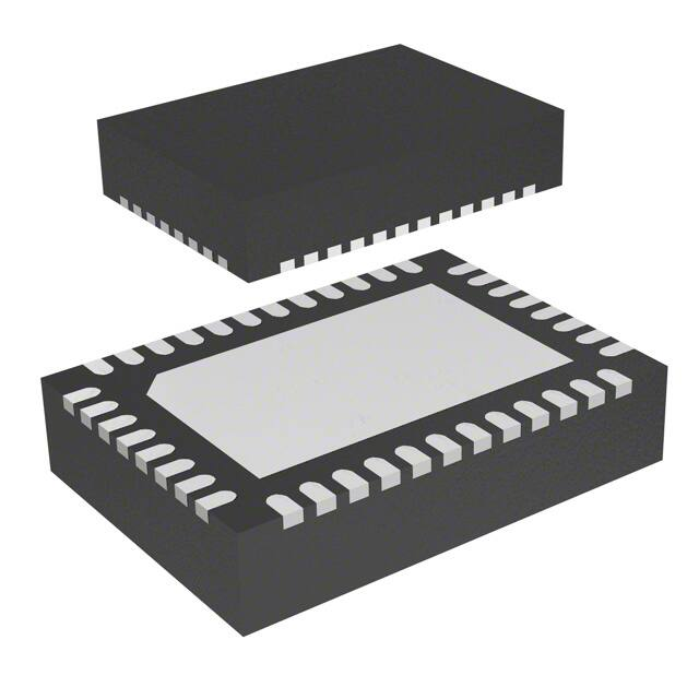


 工商网监
湘ICP备2023018690号
工商网监
湘ICP备2023018690号

