Order
Now
Product
Folder
Support &
Community
Tools &
Software
Technical
Documents
TPS562210A, TPS563210A
ZHCSFR5 – NOVEMBER 2016
TPS56x210A 采用 8 引脚 SOT-23 封装的
4.5V 至 17V 输入、2A/3A 同步降压稳压器
1 特性
3 说明
•
TPS562210A 和 TPS563210A 是采用 8 引脚 SOT-23
封装的简单易用型 2A/3A 同步降压转换器。
1
•
•
•
•
•
•
•
•
•
•
•
•
•
•
TPS562210A:集成有
133mΩ 和 80mΩ 场效应晶体管 (FET) 的 2A 转换
器
TPS563210A:集成有
68mΩ 和 39mΩ FET 的 3A 转换器
D-CAP2™针对快速瞬态响应的模式控制
高级 Eco-mode™脉冲跳跃
输入电压范围:4.5V 至 17V
输出电压范围:0.76V 至 7V
650kHz 开关频率
低关断电流(低于 10µA)
1% 反馈电压精度 (25°C)
从预偏置输出电压中启动
逐周期过流限制
断续模式欠压保护
非锁存过压保护 (OVP),欠压闭锁 (UVLO) 和热关
断 (TSD) 保护
可调软启动
电源正常输出
两款器件均经过优化,最大限度地减少了运行所需的外
部组件并且可以实现低待机电流。
这些开关模式电源 (SMPS) 器件采用 D-CAP2™ 模式
控制,从而提供快速瞬态响应,并且在无需外部补偿组
件的情况下支持诸如高分子聚合物等低等效串联电阻
(ESR) 输出电容器以及超低 ESR 陶瓷电容器。
该器件可在高级 Eco-mode™ 下运行,从而能在轻载
运行期间保持高效率。TPS562210A 和 TPS563210A
采用 8 引脚 1.6mm × 2.9mm SOT (DDF) 封装,额定
环境温度范围为 –40°C 至 85°C。
器件信息(1)
订货编号
TPS562210A
TPS563210A
封装
封装尺寸(标称值)
DDF(8)
1.60mm x 2.90mm
(1) 要了解所有可用封装,请参见数据表末尾的可订购产品附录。
2 应用
•
•
•
•
数字电视电源
高清 蓝光 (Blu-ray) 碟片™播放器
网络家庭终端设备
数字机顶盒(STB)
空白
空白
简化电路原理图
效率
TPS562210A
TPS563210A
1
2
VOUT
GND
100
VBST
SW
EN
VIN
VFB
PG
SS
90
8
7
80
EN
3
4
6
VOUT
5
Efficiency (%)
70
VIN
60
50
40
30
Copyright © 2016, Texas Instruments Incorporated
Vout = 5V
20
Vout = 3.3V
10
0
0.001
Vout = 1.8V
0.01
0.1
1
Output Current (A)
10
C015
1
An IMPORTANT NOTICE at the end of this data sheet addresses availability, warranty, changes, use in safety-critical applications,
intellectual property matters and other important disclaimers. PRODUCTION DATA.
English Data Sheet: SLVSDP9
�TPS562210A, TPS563210A
ZHCSFR5 – NOVEMBER 2016
www.ti.com.cn
目录
1
2
3
4
5
6
7
特性 ..........................................................................
应用 ..........................................................................
说明 ..........................................................................
修订历史记录 ...........................................................
Pin Configuration and Functions .........................
Specifications.........................................................
1
1
1
2
3
4
6.1
6.2
6.3
6.4
6.5
6.6
6.7
4
4
4
4
5
5
6
Absolute Maximum Ratings ......................................
ESD Ratings ............................................................
Recommended Operating Conditions.......................
Thermal Information ..................................................
Electrical Characteristics...........................................
Timing Requirements ................................................
Typical Characteristics ..............................................
7.4 Device Functional Modes........................................ 12
8
Application and Implementation ........................ 13
8.1 Application Information............................................ 13
8.2 Typical Application ................................................. 13
9 Power Supply Recommendations...................... 21
10 Layout................................................................... 22
10.1 Layout Guidelines ................................................. 22
10.2 Layout Example .................................................... 22
11 器件和文档支持 ..................................................... 23
11.1
11.2
11.3
11.4
11.5
11.6
11.7
Detailed Description ............................................ 10
7.1 Overview ................................................................. 10
7.2 Functional Block Diagram ...................................... 10
7.3 Feature Description................................................. 11
器件支持 ...............................................................
相关链接................................................................
接收文档更新通知 .................................................
社区资源................................................................
商标 .......................................................................
静电放电警告.........................................................
Glossary ................................................................
23
23
23
23
23
23
23
12 机械、封装和可订购信息 ....................................... 23
4 修订历史记录
2
日期
修订版本
注释
2016 年 11 月
*
最初发布版本。
版权 © 2016, Texas Instruments Incorporated
�TPS562210A, TPS563210A
www.ti.com.cn
ZHCSFR5 – NOVEMBER 2016
5 Pin Configuration and Functions
DDF Package
8 Pin
Top View
1
GND
2
SW
EN
7
3
VIN
VFB
6
4
PG
SS
5
VBST
8
Pin Functions
PIN
NAME
DESCRIPTION
NO.
GND
1
Ground pin Source terminal of low-side power NFET as well as the ground terminal for controller circuit. Connect
sensitive VFB to this GND at a single point.
SW
2
Switch node connection between high-side NFET and low-side NFET.
VIN
3
Input voltage supply pin. The drain terminal of high-side power NFET.
PG
4
Power good open drain output
SS
5
Soft-start control. An external capacitor should be connected to GND.
VFB
6
Converter feedback input. Connect to output voltage with feedback resistor divider.
EN
7
Enable input control. Active high and must be pulled up to enable the device.
VBST
8
Supply input for the high-side NFET gate drive circuit. Connect 0.1 µF capacitor between VBST and SW pins.
Copyright © 2016, Texas Instruments Incorporated
3
�TPS562210A, TPS563210A
ZHCSFR5 – NOVEMBER 2016
www.ti.com.cn
6 Specifications
6.1 Absolute Maximum Ratings
TJ = -40°C to 150°C (unless otherwise noted)
Input voltage range
(1)
MIN
MAX
UNIT
VIN, EN
–0.3
19
V
VBST
–0.3
25
V
VBST (10 ns transient)
–0.3
27.5
V
VBST (vs SW)
–0.3
6.5
V
VFB, PG
–0.3
6.5
V
SS
–0.3
5.5
V
SW
–2
19
V
–3.5
21
V
Operating junction temperature, TJ
SW (10 ns transient)
–40
150
°C
Storage temperature, Tstg
–55
150
°C
(1)
Stresses beyond those listed under Absolute Maximum Ratings may cause permanent damage to the device. These are stress ratings
only, which do not imply functional operation of the device at these or any other conditions beyond those indicated under Recommended
Operating Conditions. Exposure to absolute-maximum-rated conditions for extended periods may affect device reliability.
6.2 ESD Ratings
V(ESD)
(1)
(2)
Electrostatic discharge
VALUE
UNIT
Human body model (HBM), per ANSI/ESDA/JEDEC JS-001 (1)
±2000
V
Charged device model (CDM), per JEDEC specification JESD22-C101 (2)
±500
V
JEDEC document JEP155 states that 500-V HBM allows safe manufacturing with a standard ESD control process.
JEDEC document JEP157 states that 250-V CDM allows safe manufacturing with a standard ESD control process.
6.3 Recommended Operating Conditions
TJ = –40°C to 150°C (unless otherwise noted)
VIN
MIN
MAX
4.5
17
V
VBST
–0.1
23
V
VBST (10 ns transient)
–0.1
26
V
VBST(vs SW)
–0.1
6
V
EN
–0.1
17
V
VFB, pg
–0.1
5.5
V
SS
–0.1
5
V
SW
–1.8
17
V
SW (10 ns transient)
–3.5
20
V
–40
85
°C
Supply input voltage range
VI
Input voltage range
TA
Operating free-air temperature
UNIT
6.4 Thermal Information
THERMAL METRIC (1)
TPS562210A
TPS563210A
DDF (8 PINS)
UNIT
RθJA
Junction-to-ambient thermal resistance
106.1
87.0
°C/W
RθJC(top)
Junction-to-case (top) thermal resistance
49.1
41.6
°C/W
RθJB
Junction-to-board thermal resistance
10.9
14.6
°C/W
ψJT
Junction-to-top characterization parameter
8.6
4.7
°C/W
ψJB
Junction-to-board characterization parameter
10.8
14.6
°C/W
(1)
4
For more information about traditional and new thermal metrics, see the Semiconductor and IC Package Thermal Metrics application
report.
Copyright © 2016, Texas Instruments Incorporated
�TPS562210A, TPS563210A
www.ti.com.cn
ZHCSFR5 – NOVEMBER 2016
6.5 Electrical Characteristics
over operating free-air temperature range, VIN = 12 V (unless otherwise noted)
PARAMETER
TEST CONDITIONS
MIN
TYP
MAX
UNIT
SUPPLY CURRENT
IVIN
Operating – non-switching supply current
VIN current, TA = 25°C, EN = 5V, VFB = 0.8 V
190
290
µA
IVINSDN
Shutdown supply current
VIN current, TA = 25°C, EN = 0 V
3.0
10
µA
LOGIC THRESHOLD
VENH
EN high-level input voltage
EN
VENL
EN low-level input voltage
EN
REN
EN pin resistance to GND
VEN = 12 V
1.6
V
225
450
0.6
V
900
kΩ
VFB VOLTAGE AND DISCHARGE RESISTANCE
VFB threshold voltage TPS562210A
VFBTH
TA = 25°C, VO = 1.05 V, IO = 10 mA, Eco-mode™
operation
772
TA = 25°C, VO = 1.05 V
VFB threshold voltage TPS562210A and
TPS563210A
TA = 0°C to 85°C, VO = 1.05 V
758
(1)
TA = -40°C to 85°C, VO = 1.05 V (1)
IVFB
VFB input current
765
mV
772
753
777
751
779
VFB = 0.8 V, TA = 25°C
0
±0.1
mV
µA
MOSFET
RDS(on)h
High side switch resistance
RDS(on)l
Low side switch resistance
TA = 25°C, VBST – SW = 5.5 V, TPS562210A
133
TA = 25°C, VBST – SW = 5.5 V, TPS563210A
68
TA = 25°C, TPS562210A
80
TA = 25°C, TPS563210A
39
mΩ
mΩ
CURRENT LIMIT
Current limit (1)
IOCL
DC current, VOUT = 1.05 V , L1 = 2.2 µH, TPS562210A
2.5
3.2
4.3
DC current, VOUT = 1.05 V , L1 = 1.5 µH, TPS563210A
3.5
4.2
5.3
A
THERMAL SHUTDOWN
Thermal shutdown threshold (1)
TSDN
Shutdown temperature
155
Hysteresis
°C
35
SOFT START
ISS
SS charge current
VSS = 1.2 V
4.2
6
7.8
85%
90%
95%
µA
POWER GOOD
VTHPG
PG threshold
IPG
PG sink current
VFB rising (Good)
VFB falling (Fault)
85%
PG = 0.5 V
0.5
1
mA
OUTPUT UNDERVOLTAGE AND OVERVOLTAGE PROTECTION
125%x
Vfbth
VOVP
Output OVP threshold
OVP Detect
VUVP
Output UVP threshold
Hiccup detect
tHiccupOn
Hiccup Power On Time
Relative to soft start time
1
cycle
tHiccupOff
Hiccup Power Off Time
Relative to soft start time
7
cycles
65%x
Vfbth
UVLO
UVLO
(1)
UVLO threshold
Wake up VIN voltage
3.45
3.75
4.05
Hysteresis VIN voltage
0.13
0.32
0.55
V
Not production tested.
6.6 Timing Requirements
MIN
TYP
MAX
UNIT
ON-TIME TIMER CONTROL
tON
On time
VIN = 12 V, VO = 1.05 V
150
tOFF(MIN)
Minimum off time
TA = 25°C, VFB = 0.5 V
260
Copyright © 2016, Texas Instruments Incorporated
ns
310
ns
5
�TPS562210A, TPS563210A
ZHCSFR5 – NOVEMBER 2016
www.ti.com.cn
6.7 Typical Characteristics
6.7.1 TPS562210A Characteristics
VIN = 12 V (unless otherwise noted)
6
IVCCSHDN - Supply Current (µA)
300
ICC - Supply Current(µA)
250
200
150
100
50
0
4
3
2
1
0
±50
0
50
100
150
Junction Temperature (ƒC)
50
100
150
Junction Temperature (ƒC)
C012
图 2. VIN Shutdown Current vs Junction Temperature
60
0.775
50
EN Input Current (µA)
0.780
0.770
0.765
0.760
40
30
20
10
0.755
0
0.750
-10
±50
0
50
100
0
150
Junction Temperature (ƒC)
3
90
80
80
70
70
Efficiency (%)
100
60
50
40
15
C014
60
50
40
20
Vout = 3.3V
Vout = 3.3V
10
10
Vout = 1.8V
0.01
0.1
1
Output Current (A)
18
30
Vout = 5V
20
12
图 4. EN Current vs EN Voltage
90
30
9
EN Input Voltage (V)
100
0
0.001
6
C013
图 3. VFB Voltage vs Junction Temperature
Efficiency (%)
0
±50
C011
图 1. Supply Current vs Junction Temperature
VFB Voltage (V)
5
10
Vout = 1.8V
0
0.001
0.01
0.1
1
Output Current(A)
C015
10
C016
VI = 5 V
图 5. Efficiency vs Output Current
6
图 6. Efficiency vs Output Current
版权 © 2016, Texas Instruments Incorporated
�TPS562210A, TPS563210A
www.ti.com.cn
ZHCSFR5 – NOVEMBER 2016
TPS562210A Characteristics (接
接下页)
800
800
Vo = 0.76V
FSW - Switching Frequency
750
FSW - Switching Frequency (kHz)
Vo = 0.75V
Vo = 1.05V
700
Vo = 6.5V
650
600
550
500
450
400
4
6
8
10
12
14
16
Input Voltage (V)
图 7. Switching Frequency vs Input Voltage
版权 © 2016, Texas Instruments Incorporated
18
C017
700
Vo = 1.05V
600
Vo = 6.5V
500
400
300
200
100
0
0.01
0.1
1
Output Current (A)
10
C018
图 8. Switching Frequency vs Output Current
7
�TPS562210A, TPS563210A
ZHCSFR5 – NOVEMBER 2016
www.ti.com.cn
6.7.2 TPS563210A Characteristics
VIN = 12V (unless otherwise noted)
6
IVCCSHDN - Supply Current (µA)
300
ICC - Supply Current (µA)
250
200
150
100
50
0
4
3
2
1
0
±50
0
50
100
150
Junction Temperature (ƒC)
50
100
150
Junction Temperature (ƒC)
C020
图 10. VIN Shutdown Current vs Junction Temperature
60
0.775
50
EN Input Current (µA)
0.780
0.770
0.765
0.760
0.755
40
30
20
10
0
0.750
±10
±50
0
50
100
0
150
Junction Temperature (ƒC)
3
90
80
80
70
70
Efficiency (%)
100
60
50
40
0.1
1
Output Current (A)
60
50
40
Vout = 3.3V
10
Vout = 1.8V
0.01
18
C022
20
Vout = 3.3V
10
15
30
Vout = 5V
20
12
图 12. EN Current vs EN Voltage
90
30
9
EN Input Voltage (V)
100
0
0.001
6
C021
图 11. VFB Voltage vs Junction Temperature
Efficiency (%)
0
±50
C019
图 9. Supply Current vs Junction Temperature
VFB Voltage (V)
5
10
Vout = 1.8V
0
0.001
0.01
0.1
1
Output Current (A)
C023
10
C024
VI = 5 V
图 13. Efficiency vs Output Current
8
图 14. Efficiency vs Output Current
版权 © 2016, Texas Instruments Incorporated
�TPS562210A, TPS563210A
www.ti.com.cn
ZHCSFR5 – NOVEMBER 2016
TPS563210A Characteristics (接
接下页)
800
800
750
Vo = 0.76V
FSW - Switching Frequency (kHz)
FSW - Switching Frequency (kHz)
Vo = 0.76V
Vo = 1.05V
700
Vo = 6.5V
650
600
550
500
450
400
4
6
8
10
12
14
16
Input Voltage (V)
图 15. Switching Frequency vs Input Voltage
版权 © 2016, Texas Instruments Incorporated
18
C025
700
Vo = 1.05V
600
Vo = 6.5V
500
400
300
200
100
0
0.01
0.1
1
Output Current (A)
10
C026
图 16. Switching Frequency vs Output Current
9
�TPS562210A, TPS563210A
ZHCSFR5 – NOVEMBER 2016
www.ti.com.cn
7 Detailed Description
7.1 Overview
The TPS562210A and TPS563210A are 2-A, 3-A synchronous step-down converters. The proprietary D-CAP2™
mode control supports low ESR output capacitors such as specialty polymer capacitors and multi-layer ceramic
capacitors without complex external compensation circuits. The fast transient response of D-CAP2™ mode
control can reduce the output capacitance required to meet a specific level of performance.
7.2 Functional Block Diagram
EN
7
VUVP
VOVP
VFB
SS
+
UVP
Hiccup
+
OVP
Control Logic
5
Ref
Soft Start
SS
VIN
8
VBST
2
SW
1
GND
VREG5
Regulator
UVLO
6
Voltage
Reference
3
+
+
PWM
HS
Ton
One-Shot
XCON
VREG 5
TSD
PG
OCL
threshold
4
LS
OCL
+
+
V THPG
+
ZC
Copyright © 2016, Texas Instruments Incorporated
10
版权 © 2016, Texas Instruments Incorporated
�TPS562210A, TPS563210A
www.ti.com.cn
ZHCSFR5 – NOVEMBER 2016
7.3 Feature Description
7.3.1 The Adaptive On-Time Control and PWM Operation
The main control loop of the TPS562210A and TPS563210A are adaptive on-time pulse width modulation (PWM)
controller that supports a proprietary D-CAP2™ mode control. The D-CAP2™ mode control combines adaptive
on-time control with an internal compensation circuit for pseudo-fixed frequency and low external component
count configuration with both low ESR and ceramic output capacitors. It is stable even with virtually no ripple at
the output.
At the beginning of each cycle, the high-side MOSFET is turned on. This MOSFET is turned off after internal one
shot timer expires. This one shot duration is set proportional to the converter input voltage, VIN, and inversely
proportional to the output voltage, VO, to maintain a pseudo-fixed frequency over the input voltage range, hence
it is called adaptive on-time control. The one-shot timer is reset and the high-side MOSFET is turned on again
when the feedback voltage falls below the reference voltage. An internal ramp is added to reference voltage to
simulate output ripple, eliminating the need for ESR induced output ripple from D-CAP2™ mode control.
7.3.2 Soft Start and Pre-Biased Soft Start
The TPS562210A and TPS563210A have adjustable soft-start. When the EN pin becomes high, the SS charge
current (ISS) begins charging the capacitor which is connected from the SS pin to GND (CSS). Smooth control of
the output voltage is maintained during start up. The equation for the soft start time, Tss is shown in 公式 1.
Css ´ VFBTH ´ 0.86
Tss(ms) =
Iss
(1)
where VFBTH is 0.765 V and Iss is 6 µA.
If the output capacitor is pre-biased at startup, the devices initiate switching and start ramping up only after the
internal reference voltage becomes greater than the feedback voltage VFB. This scheme ensures that the
converters ramp up smoothly into regulation point.
7.3.3 Power Good
The power good output, PG is an open drain output. The power good function becomes active after 1.7 times
soft-start time. When the output voltage becomes within –10% of the target value, internal comparators detect
power good state and the power good signal becomes high. If the feedback voltage goes under 15% of the target
value, the power good signal becomes low.
7.3.4 Current Protection
The output over-current limit (OCL) is implemented using a cycle-by-cycle valley detect control circuit. The switch
current is monitored during the OFF state by measuring the low-side FET drain to source voltage. This voltage is
proportional to the switch current. To improve accuracy, the voltage sensing is temperature compensated.
During the on time of the high-side FET switch, the switch current increases at a linear rate determined by VIN,
VOUT, the on-time and the output inductor value. During the on time of the low-side FET switch, this current
decreases linearly. The average value of the switch current is the load current IOUT. If the monitored current is
above the OCL level, the converter maintains low-side FET on and delays the creation of a new set pulse, even
the voltage feedback loop requires one, until the current level becomes OCL level or lower. In subsequent
switching cycles, the on-time is set to a fixed value and the current is monitored in the same manner. If the over
current condition exists consecutive switching cycles, the internal OCL threshold is set to a lower level, reducing
the available output current. When a switching cycle occurs where the switch current is not above the lower OCL
threshold, the counter is reset and the OCL threshold is returned to the higher value.
There are some important considerations for this type of over-current protection. The load current is higher than
the over-current threshold by one half of the peak-to-peak inductor ripple current. Also, when the current is being
limited, the output voltage tends to fall as the demanded load current may be higher than the current available
from the converter. This may cause the output voltage to fall. When the VFB voltage falls below the UVP
threshold voltage, the UVP comparator detects it. And then, the device will shut down after the UVP delay time
(typically 14 µs) and re-start after the hiccup time.
When the over current condition is removed, the output voltage returns to the regulated value.
版权 © 2016, Texas Instruments Incorporated
11
�TPS562210A, TPS563210A
ZHCSFR5 – NOVEMBER 2016
www.ti.com.cn
Feature Description (接
接下页)
7.3.5 Over Voltage Protection
TPS562210A and TPS563210A detect over voltage condition by monitoring the feedback voltage (VFB). When
the feedback voltage becomes higher than 125% of the target voltage, the OVP comparator output goes high
and the high-side MOSFET is turns off. This function is non-latch operation.
7.3.6 UVLO Protection
Under voltage lock out protection (UVLO) monitors the internal regulator voltage. When the voltage is lower than
UVLO threshold voltage, the device is shut off. This protection is non-latching.
7.3.7 Thermal Shutdown
The device monitors the temperature of itself. If the temperature exceeds the threshold value (typically 155°C),
the device is shut off. This is a non-latch protection.
7.4 Device Functional Modes
7.4.1 Advanced Eco-Mode™ Control
The TPS562210A and TPS563210A are designed with Advanced Eco-mode™ to maintain high light load
efficiency. As the output current decreases from heavy load condition, the inductor current is also reduced and
eventually comes to point that its rippled valley touches zero level, which is the boundary between continuous
conduction and discontinuous conduction modes. The rectifying MOSFET is turned off when the zero inductor
current is detected. As the load current further decreases the converter runs into discontinuous conduction mode.
The on-time is kept almost the same as it was in the continuous conduction mode so that it takes longer time to
discharge the output capacitor with smaller load current to the level of the reference voltage. This makes the
switching frequency lower, proportional to the load current, and keeps the light load efficiency high. The transition
point to the light load operation IOUT(LL) current can be calculated in 公式 2.
IOUT(LL) =
12
(VIN - VOUT )´ VOUT
1
´
2 ´ L ´ fSW
VIN
(2)
版权 © 2016, Texas Instruments Incorporated
�TPS562210A, TPS563210A
www.ti.com.cn
ZHCSFR5 – NOVEMBER 2016
8 Application and Implementation
注
Information in the following applications sections is not part of the TI component
specification, and TI does not warrant its accuracy or completeness. TI’s customers are
responsible for determining suitability of components for their purposes. Customers should
validate and test their design implementation to confirm system functionality.
8.1 Application Information
The TPS562210A and TPS563210A are typically used as step down converters, which convert a voltage from
4.5 V to 17 V to a lower voltage. Webench software is available to aid in the design and analysis of circuits.
8.2 Typical Application
8.2.1 Typical Application, TPS562210A
4.5-V to 17-V Input, 1.05-V Output Converter.
U1
TPS562210A
L1
VIN = 4.5 - 17 V
C1
0.1µF
2.2uH
C5
3
VIN
C2
10µF
C3
10µF
EN
R3 10.0k 7
VIN
VBST
SW
SS
VFB
PG
5
VOUT
0.1µF
EN
GND
VOUT = 1.05 V, 2 A
8
2
R4
100k
4
C6
22µF
C7
22µF
PG
C8
22µF
R1
3.74k
6
1
C4
8200pF
R2
10.0k
图 17. TPS562210A 1.05V/2A Reference Design
8.2.1.1 Design Requirements
For this design example, use the parameters shown in 表 1.
表 1. Design Parameters
PARAMETER
Input voltage range
Output voltage
Output current
Output voltage ripple
VALUES
4.5 V to 17 V
1.05 V
2A
20 mVp-p
8.2.1.2 Detailed Design Procedure
8.2.1.2.1 Output Voltage Resistors Selection
The output voltage is set with a resistor divider from the output node to the VFB pin. It is recommended to use
1% tolerance or better divider resistors. Start by using 公式 3 to calculate VOUT.
To improve efficiency at light loads consider using larger value resistors, too high of resistance are more
susceptible to noise and voltage errors from the VFB input current are more noticeable.
R1 ö
æ
VOUT = 0.765 ´ ç 1 +
÷
R2
è
ø
(3)
8.2.1.2.2 Output Filter Selection
The LC filter used as the output filter has double pole at:
1
FP =
2p LOUT ´ COUT
版权 © 2016, Texas Instruments Incorporated
(4)
13
�TPS562210A, TPS563210A
ZHCSFR5 – NOVEMBER 2016
www.ti.com.cn
At low frequencies, the overall loop gain is set by the output set-point resistor divider network and the internal
gain of the device. The low frequency phase is 180 degrees. At the output filter pole frequency, the gain rolls off
at a –40 dB per decade rate and the phase drops rapidly. D-CAP2™ introduces a high frequency zero that
reduces the gain roll off to –20 dB per decade and increases the phase to 90 degrees one decade above the
zero frequency. The inductor and capacitor for the output filter must be selected so that the double pole of 公式 4
is located below the high frequency zero but close enough that the phase boost provided be the high frequency
zero provides adequate phase margin for a stable circuit. To meet this requirement use the values recommended
in 表 2.
表 2. TPS562210A Recommended Component Values
Output Voltage (V)
R2 (kΩ)
R3 (kΩ)
1
3.09
1.05
1.2
L1 (µH)
C6 + C7 + C8 (µF)
MIN
TYP
MAX
10.0
1.5
2.2
4.7
20 - 68
3.74
10.0
1.5
2.2
4.7
20 - 68
5.76
10.0
1.5
2.2
4.7
20 - 68
1.5
9.53
10.0
1.5
2.2
4.7
20 - 68
1.8
13.7
10.0
1.5
2.2
4.7
20 - 68
2.5
22.6
10.0
2.2
3.3
4.7
20 - 68
3.3
33.2
10.0
2.2
3.3
4.7
20 - 68
5
54.9
10.0
3.3
4.7
4.7
20 - 68
6.5
75
10.0
3.3
4.7
4.7
20 - 68
The inductor peak-to-peak ripple current, peak current and RMS current are calculated using 公式 5, 公式 6 and
公式 7. The inductor saturation current rating must be greater than the calculated peak current and the RMS or
heating current rating must be greater than the calculated RMS current.
Use 650 kHz for fSW. Make sure the chosen inductor is rated for the peak current of 公式 6 and the RMS current
of 公式 7.
VIN(MAX) - VOUT
VOUT
´
IlP -P =
VIN(MAX)
LO ´ ƒSW
(5)
IlPEAK = IO +
IlP -P
2
ILO(RMS) = IO2 +
1
IlP -P2
12
(6)
(7)
For this design example, the calculated peak current is 2.34 A and the calculated RMS current is 2.01 A. The
inductor used is a TDK CLF7045T-2R2N with a peak current rating of 5.5 A and an RMS current rating of 4.3 A.
The capacitor value and ESR determines the amount of output voltage ripple. The TPS562210A and
TPS563210A are intended for use with ceramic or other low ESR capacitors. Recommended values range from
20µF to 68µF. Use 公式 8 to determine the required RMS current rating for the output capacitor.
ICO(RMS) =
VOUT ´ (VIN - VOUT )
12 ´ VIN ´ LO ´ ƒSW
(8)
For this design, two TDK C3216X5R0J226M 22 µF output capacitors are used. The typical ESR is 2 mΩ each.
The calculated RMS current is 0.286A and each output capacitor is rated for 4A.
8.2.1.2.3 Input Capacitor Selection
The TPS562210A and TPS563210A require an input decoupling capacitor and a bulk capacitor is needed
depending on the application. A ceramic capacitor over 10 µF is recommended for the decoupling capacitor. An
additional 0.1 µF capacitor (C3) from pin 3 to ground is optional to provide additional high frequency filtering. The
capacitor voltage rating needs to be greater than the maximum input voltage.
14
版权 © 2016, Texas Instruments Incorporated
�TPS562210A, TPS563210A
www.ti.com.cn
ZHCSFR5 – NOVEMBER 2016
8.2.1.2.4 Bootstrap capacitor Selection
A 0.1µF ceramic capacitor must be connected between the VBST to SW pin for proper operation. It is
recommended to use a ceramic capacitor.
8.2.1.3 Application Curves
100
100
90
90
80
80
70
70
Efficiency (%)
Efficiency (%)
The following application curves were generated using the application circuit of 图 17.
60
50
40
30
60
50
40
30
20
20
VIN = 5V
VIN = 12V
10
0
0
0.5
1
Output Current (A)
1.5
VIN = 5V
VIN = 12V
10
0
0.001
2
D006
1
1
0.8
0.8
0.6
0.6
0.4
0.2
0
-0.2
-0.4
1
2 3 45
D007
0.4
0.2
0
-0.2
-0.4
-0.6
-0.6
-0.8
-0.8
-1
-1
0
0.5
1
Output Current (A)
1.5
2
0
0.5
D008
图 20. TPS562210A Load Regulation, VI = 5 V
1
Output Current (A)
1.5
2
D009
图 21. TPS562210A Load Regulation, VI = 12 V
0.5
IO = 2 A
0.4
VI = 50 mV / div (ac coupled)
0.3
Line Regulation (%)
0.5
图 19. TPS562210A Light Load Efficiency
Load Regulation (%)
Load Regulation (%)
图 18. TPS562210A Efficiency
0.01 0.02 0.05 0.1 0.2
Output Current (A)
0.2
0.1
0
SW = 5 V / div
-0.1
-0.2
-0.3
-0.4
-0.5
4
6
8
10
12
Input Voltage (V)
14
16
图 22. TPS562210A Line Regulation
版权 © 2016, Texas Instruments Incorporated
18
D010
Time = 1 µsec / div
图 23. TPS562210A Input Voltage Ripple
15
�TPS562210A, TPS563210A
ZHCSFR5 – NOVEMBER 2016
www.ti.com.cn
IO = 200 mA
IO = 0 A
VO = 20 mV / div (ac coupled)
VO = 20 mV / div (ac coupled)
SW = 5 V / div
SW = 5 V / div
Time = 5 msec / div
图 24. TPS562210A Output Voltage Ripple
Time = 1 µsec / div
图 25. TPS562210A Output Voltage Ripple
IO = 2 A
VO = 20 mV / div (ac coupled)
VO = 50 mV / div (ac coupled)
IO = 500 mA / div
SW = 5 V / div
Load step = 0.5 A - 1.5 A
Slew rate = 500 mA / µsec
Time = 1 µsec / div
图 26. TPS562210A Output Voltage Ripple
VI = 10V/ div
EN = 10V/ div
SS = 5V/ div
SS = 5V/ div
VO = 500mV/ div
VO = 500mV/ div
PG = 1V/ div
PG = 1V/ div
Time = 1 msec / div
图 28. TPS562210A Start Up Relative To VI
16
Time = 200 µsec / div
图 27. TPS562210A Transient Response
Time = 1 msec / div
图 29. TPS562210A Start Up Relative To En
版权 © 2016, Texas Instruments Incorporated
�TPS562210A, TPS563210A
www.ti.com.cn
ZHCSFR5 – NOVEMBER 2016
VI = 10V/ div
EN = 10V/ div
SS = 5V/ div
SS = 5V/ div
VO = 500mV/ div
VO = 500mV/ div
PG = 1V/ div
PG = 1V/ div
Time = 5 msec / div
图 30. TPS562210A Shut Down Relative To VI
版权 © 2016, Texas Instruments Incorporated
Time = 5 msec / div
图 31. TPS562210A Shut Down Relative To EN
17
�TPS562210A, TPS563210A
ZHCSFR5 – NOVEMBER 2016
www.ti.com.cn
8.2.2 Typical Application, TPS563210A
4.5-V To 17-V Input, 1.05-V Output Converter.
U1
TPS563210A
L1
VIN = 4.5 - 17 V
VIN
C1
0.1µF
1.5uH
C5
3
C2
10µF
C3
10µF
R3 10.0k 7
EN
VIN
VBST
VOUT
0.1µF
EN
SW
PG
5
VOUT = 1.05 V, 3 A
8
SS
VFB
GND
R4
100k
2
4
C6
22µF
C7
22µF
PG
C8
22µF
R1
3.74k
6
1
C4
8200pF
R2
10.0k
图 32. TPS563210A 1.05 V / 3A Reference Design
8.2.2.1
Design Requirements
For this design example, use the parameters shown in 表 3.
表 3. Design Parameters
PARAMETER
VALUE
Input voltage range
4.5 V to 17 V
Output voltage
1.05 V
Output current
3A
Output voltage ripple
20 mVpp
8.2.2.2 Detailed Design Procedures
The detailed design procedure for TPS563210A is the same as for TPS562210A except for inductor selection.
8.2.2.2.1 Output Filter Selection
表 4. TPS563210A Recommended Component Values
Output Voltage (V)
R2 (kΩ)
R3 (kΩ)
L1 (µH)
MIN
TYP
MAX
C6 + C7 + C8 (µF)
1
3.09
10.0
1.0
1.5
4.7
20 - 68
1.05
3.74
10.0
1.0
1.5
4.7
20 - 68
1.2
5.76
10.0
1.0
1.5
4.7
20 - 68
1.5
9.53
10.0
1.0
1.5
4.7
20 - 68
1.8
13.7
10.0
1.5
2.2
4.7
20 - 68
2.5
22.6
10.0
1.5
2.2
4.7
20 - 68
3.3
33.2
10.0
1.5
2.2
4.7
20 - 68
5
54.9
10.0
2.2
3.3
4.7
20 - 68
6.5
75
10.0
2.2
3.3
4.7
20 - 68
The inductor peak-to-peak ripple current, peak current and RMS current are calculated using 公式 9, 公式 10 and
公式 11. The inductor saturation current rating must be greater than the calculated peak current and the RMS or
heating current rating must be greater than the calculated RMS current. Use 650 kHz for ƒSW.
Use 650 kHz for ƒSW. Make sure the chosen inductor is rated for the peak current of 公式 10 and the RMS
current of 公式 11.
VIN(MAX) - VOUT
VOUT
´
IlP -P =
VIN(MAX)
LO ´ ƒSW
(9)
18
版权 © 2016, Texas Instruments Incorporated
�TPS562210A, TPS563210A
www.ti.com.cn
ZHCSFR5 – NOVEMBER 2016
IlPEAK = IO +
IlP -P
2
ILO(RMS) = IO2 +
(10)
1
IlP -P2
12
(11)
For this design example, the calculated peak current is 3.505 A and the calculated RMS current is 3.014 A. The
inductor used is a TDK CLF7045T-1R5N with a peak current rating of 7.3-A and an RMS current rating of 4.9-A.
The capacitor value and ESR determines the amount of output voltage ripple. The TPS563209 is intended for
use with ceramic or other low ESR capacitors. Recommended values range from 20 μF to 68 μF. Use 公式 7 to
determine the required RMS current rating for the output capacitor. For this design three TDK C3216X5R0J226M
22 μF output capacitors are used. The typical ESR is 2 mΩ each. The calculated RMS current is 0.292A and
each output capacitor is rated for 4 A.
8.2.2.3 Application Curves
100
100
90
90
80
80
70
70
Efficiency (%)
Efficiency (%)
The following application curves were generated using the application circuit of 图 32.
60
50
40
60
50
40
30
30
20
20
VIN = 5V
VIN = 12V
10
0
0.001
0
0
0.5
1
1.5
2
Output Current (A)
2.5
VIN = 5V
VIN = 12V
10
3
图 33. TPS563210A Efficiency
0.5
1
2 3 45
D002
图 34. TPS563210A Light Load Efficiency
1
1
0.8
0.8
0.6
0.6
Load Regulation (%)
Load Regulation (%)
0.01 0.02 0.05 0.1 0.2
Output Current (A)
D001
0.4
0.2
0
-0.2
-0.4
0.4
0.2
0
-0.2
-0.4
-0.6
-0.6
-0.8
-0.8
-1
-1
0
0.5
1
1.5
2
Output Current (A)
2.5
图 35. TPS563210A Load Regulation, VI = 5 V
版权 © 2016, Texas Instruments Incorporated
3
D003
0
0.5
1
1.5
2
Output Current (A)
2.5
3
D004
图 36. TPS563210A Load Regulation, VI = 12 V
19
�TPS562210A, TPS563210A
ZHCSFR5 – NOVEMBER 2016
www.ti.com.cn
0.5
IO = 3 A
0.4
VI = 50 mV / div (ac coupled)
Line Regulation (%)
0.3
0.2
0.1
0
SW = 5 V / div
-0.1
-0.2
-0.3
-0.4
-0.5
4
6
8
10
12
Input Voltage (V)
14
16
18
D005
图 37. TPS563210A Line Regulation
Time = 1 µsec / div
图 38. TPS563210A Input Voltage Ripple
IO = 300 mA
IO = 0 A
VO = 20 mV / div (ac coupled)
VO = 20 mV / div (ac coupled)
SW = 5 V / div
SW = 5 V / div
Time = 5 msec / div
图 39. TPS563210A Output Voltage Ripple
Time = 1 µsec / div
图 40. TPS563210A Output Voltage Ripple
IO = 3 A
VO = 20 mV / div (ac coupled)
SW = 5 V / div
VO = 50 mV / div (ac coupled)
IO = 1 A / div
Load step = 0.75 A - 2.25 A
Slew rate = 500 mA / µsec
Time = 1 µsec / div
图 41. TPS563210A Output Voltage Ripple
20
Time = 200 µsec / div
图 42. TPS563210A Transient Response
版权 © 2016, Texas Instruments Incorporated
�TPS562210A, TPS563210A
www.ti.com.cn
ZHCSFR5 – NOVEMBER 2016
VI = 10V/ div
EN = 10V/ div
SS = 5V/ div
SS = 5V/ div
VO = 500mV/ div
VO = 500mV/ div
PG = 1V/ div
PG = 1V/ div
Time = 1 msec / div
图 43. TPS563210A Start Up Relative To VI
Time = 1 msec / div
图 44. TPS563210A Start Up Relative To EN
VI = 10V/ div
EN = 10V/ div
SS = 5V/ div
SS = 5V/ div
VO = 500mV/ div
VO = 500mV/ div
PG = 1V/ div
PG = 1V/ div
Time = 5 msec / div
图 45. TPS563210A Shut Down Relative To VI
Time = 5 msec / div
图 46. TPS563210A Shut Down Relative To EN
9 Power Supply Recommendations
The TPS562210A and TPS563210A are designed to operate from input supply voltage in the range of 4.5 V to
17 V. Buck converters require the input voltage to be higher than the output voltage for proper operation. The
maximum recommended operating duty cycle is 65%. Using that criteria, the minimum recommended input
voltage is VO / 0.65.
版权 © 2016, Texas Instruments Incorporated
21
�TPS562210A, TPS563210A
ZHCSFR5 – NOVEMBER 2016
www.ti.com.cn
10 Layout
10.1 Layout Guidelines
1. VIN and GND traces should be as wide as possible to reduce trace impedance. The wide areas are also of
advantage from the view point of heat dissipation.
2. The input capacitor and output capacitor should be placed as close to the device as possible to minimize
trace impedance.
3. Provide sufficient vias for the input capacitor and output capacitor.
4. Keep the SW trace as physically short and wide as practical to minimize radiated emissions.
5. Do not allow switching current to flow under the device.
6. A separate VOUT path should be connected to the upper feedback resistor.
7. Make a Kelvin connection to the GND pin for the feedback path.
8. Voltage feedback loop should be placed away from the high-voltage switching trace, and preferably has
ground shield.
9. The trace of the VFB node should be as small as possible to avoid noise coupling.
10. The GND trace between the output capacitor and the GND pin should be as wide as possible to minimize its
trace impedance.
10.2 Layout Example
GND
VOUT
Additional
Vias to the
GND plane
OUTPUT
CAPACITOR
Vias to the
internal SW
node copper
BOOST
CAPACITOR
OUTPUT
INDUCTOR
GND
VBST
SW
EN
FEEDBACK
RESISTORS
TO ENABLE
CONTROL
TPS56x10A
VIN
Vias to the
internal SW
node copper
SW node copper
pour area on internal
or bottom layer
HIGH FREQUENCY
INPUT BYPASS
CAPACITOR
INPUT BYPASS
CAPACITOR
VIN
VFB
SS
PG
SLOW START
CAPACITOR
VIA TO INTERNAL
GROUND PLANE
22
POWER GOOD
PG PULL UP
RESISTOR
TO PG PULL
UP VOLTAGE
版权 © 2016, Texas Instruments Incorporated
�TPS562210A, TPS563210A
www.ti.com.cn
ZHCSFR5 – NOVEMBER 2016
11 器件和文档支持
11.1 器件支持
11.2 相关链接
下面的表格列出了快速访问链接。范围包括技术文档、支持和社区资源、工具和软件,以及样片或购买的快速访
问。
表 5. 相关链接
器件
产品文件夹
样片与购买
技术文档
工具与软件
支持与社区
TPS562210A
请单击此处
请单击此处
请单击此处
请单击此处
请单击此处
TPS563210A
请单击此处
请单击此处
请单击此处
请单击此处
请单击此处
11.3 接收文档更新通知
如需接收文档更新通知,请访问 www.ti.com.cn 网站上的器件产品文件夹。点击右上角的提醒我 (Alert me) 注册
后,即可每周定期收到已更改的产品信息。有关更改的详细信息,请查阅已修订文档中包含的修订历史记录。
11.4 社区资源
The following links connect to TI community resources. Linked contents are provided "AS IS" by the respective
contributors. They do not constitute TI specifications and do not necessarily reflect TI's views; see TI's Terms of
Use.
TI E2E™ Online Community TI's Engineer-to-Engineer (E2E) Community. Created to foster collaboration
among engineers. At e2e.ti.com, you can ask questions, share knowledge, explore ideas and help
solve problems with fellow engineers.
Design Support TI's Design Support Quickly find helpful E2E forums along with design support tools and
contact information for technical support.
11.5 商标
D-CAP2, Eco-mode, E2E are trademarks of Texas Instruments.
蓝光 (Blu-ray) 碟片 is a trademark of Blu-ray Disc Association.
11.6 静电放电警告
ESD 可能会损坏该集成电路。德州仪器 (TI) 建议通过适当的预防措施处理所有集成电路。如果不遵守正确的处理措施和安装程序 , 可
能会损坏集成电路。
ESD 的损坏小至导致微小的性能降级 , 大至整个器件故障。 精密的集成电路可能更容易受到损坏 , 这是因为非常细微的参数更改都可
能会导致器件与其发布的规格不相符。
11.7 Glossary
SLYZ022 — TI Glossary.
This glossary lists and explains terms, acronyms, and definitions.
12 机械、封装和可订购信息
以下页中包括机械、封装和可订购信息。这些信息是针对指定器件可提供的最新数据。这些数据会在无通知且不对
本文档进行修订的情况下发生改变。欲获得该数据表的浏览器版本,请查阅左侧的导航栏。
版权 © 2016, Texas Instruments Incorporated
23
�PACKAGE OPTION ADDENDUM
www.ti.com
10-Dec-2020
PACKAGING INFORMATION
Orderable Device
Status
(1)
Package Type Package Pins Package
Drawing
Qty
Eco Plan
(2)
Lead finish/
Ball material
MSL Peak Temp
Op Temp (°C)
Device Marking
(3)
(4/5)
(6)
TPS562210ADDFR
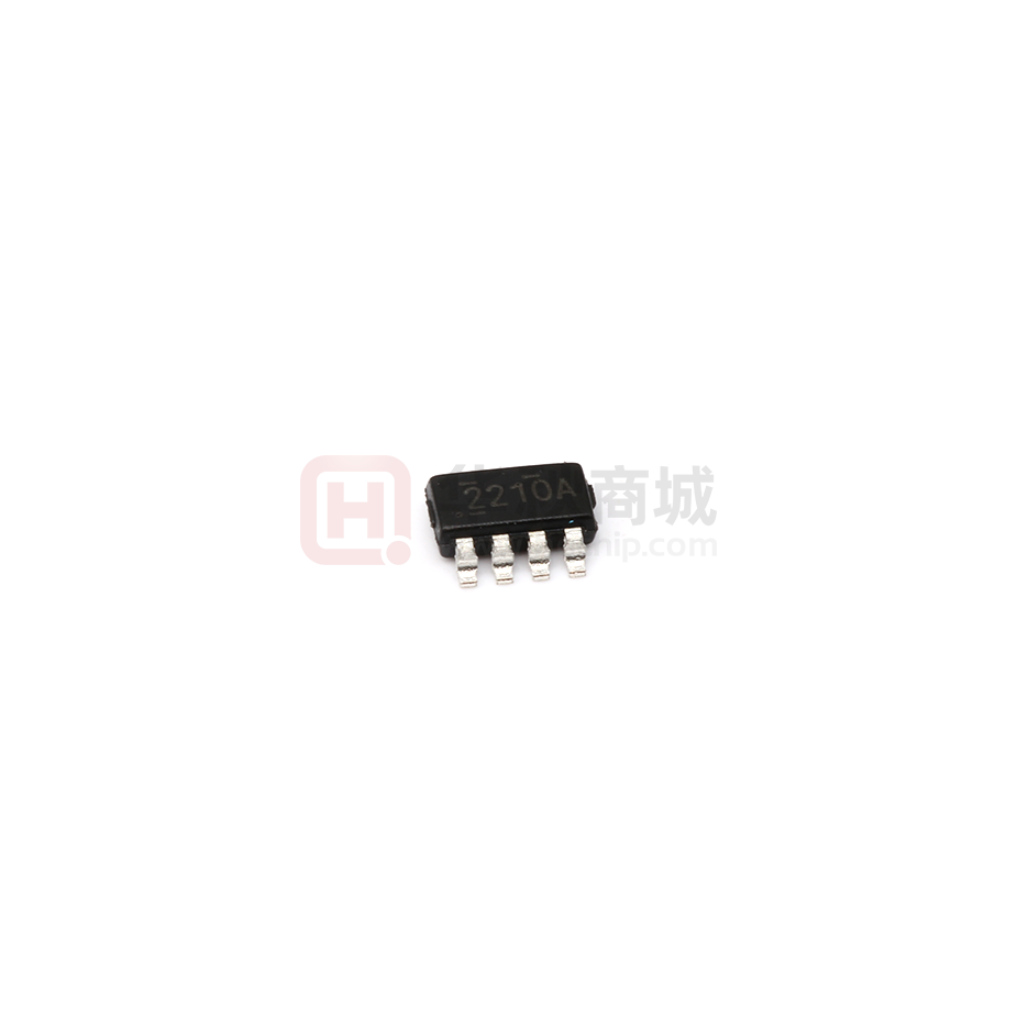
ACTIVE
SOT-23-THIN
DDF
8
3000
RoHS & Green
SN
Level-1-260C-UNLIM
-40 to 85
2210A
TPS562210ADDFT
ACTIVE
SOT-23-THIN
DDF
8
250
RoHS & Green
SN
Level-1-260C-UNLIM
-40 to 85
2210A
TPS563210ADDFR
ACTIVE
SOT-23-THIN
DDF
8
3000
RoHS & Green
SN
Level-1-260C-UNLIM
-40 to 85
3210A
TPS563210ADDFT
ACTIVE
SOT-23-THIN
DDF
8
250
RoHS & Green
SN
Level-1-260C-UNLIM
-40 to 85
3210A
(1)
The marketing status values are defined as follows:
ACTIVE: Product device recommended for new designs.
LIFEBUY: TI has announced that the device will be discontinued, and a lifetime-buy period is in effect.
NRND: Not recommended for new designs. Device is in production to support existing customers, but TI does not recommend using this part in a new design.
PREVIEW: Device has been announced but is not in production. Samples may or may not be available.
OBSOLETE: TI has discontinued the production of the device.
(2)
RoHS: TI defines "RoHS" to mean semiconductor products that are compliant with the current EU RoHS requirements for all 10 RoHS substances, including the requirement that RoHS substance
do not exceed 0.1% by weight in homogeneous materials. Where designed to be soldered at high temperatures, "RoHS" products are suitable for use in specified lead-free processes. TI may
reference these types of products as "Pb-Free".
RoHS Exempt: TI defines "RoHS Exempt" to mean products that contain lead but are compliant with EU RoHS pursuant to a specific EU RoHS exemption.
Green: TI defines "Green" to mean the content of Chlorine (Cl) and Bromine (Br) based flame retardants meet JS709B low halogen requirements of


 工商网监
湘ICP备2023018690号
工商网监
湘ICP备2023018690号
