��������
��
����
����� ������ ���������
���� � �
��
��
� ���������
SLVS214B − JUNE 1999 − REVISED AUGUST 2008
features
D
D
D
D
D
D
D
D
D
D
D
D
applications
Up to 100-mA Output Current
Less Than 5-mVpp Output Voltage Ripple
No Inductors Required/Low EMI
Regulated 3.3-V ±4% Output
Only Four External Components Required
Up to 90% Efficiency
1.8-V to 3.6-V Input Voltage Range
50-µA Quiescent Supply Current
0.05-µA Shutdown Current
Load Isolated in Shutdown
Space-Saving Thermally-Enhanced TSSOP
PowerPAD Package
Evaluation Module Available
(TPS60100EVM−131)
Replaces DC/DC Converters With Inductors in
− Battery-Powered Applications
− Two Battery Cells to 3.3-V Conversion
− Portable Instruments
− Battery-Powered Microprocessor and
DSP Systems
− Miniature Equipment
− Backup-Battery Boost Converters
− PDAs
− Laptops
− Handheld Instrumentation
− Medical Instruments
− Cordless Phones
output voltage ripple
description
3.45
The TPS60101 features either constant frequency mode to minimize noise and output voltage
ripple or the power-saving pulse-skip mode to
extend battery life at light loads. The TPS60101
switching frequency is 300 kHz. The logic
shutdown function reduces the supply current to
1-µA (max) and disconnects the load from the
input. Special current-control circuitry prevents
excessive current from being drawn from the
battery during start-up. This DC/DC converter
requires no inductors and has low EMI. It is
available in the small 20-pin TSSOP PowerPAD
package (PWP).
3.4
VO − Output Voltage − V
The TPS60101 step-up, regulated charge pump
generates a 3.3-V ±4% output voltage from a
1.8-V to 3.6-V input voltage (two alkaline, NiCd, or
NiMH batteries). Output current is 100 mA from a
2-V input. Only four external capacitors are
needed to build a complete low-noise dc/dc
converter. The push-pull operating mode of two
single-ended charge pumps assures the low
output voltage ripple as current is continuously
transferred to the output. From a 2-V input, the
TPS60101 can start into full load with loads as low
as 33 Ω.
3.35
3.3
3.25
SKIP =COM = 3V8 = 0 V
VIN = 2.4 V
VO = 3.3 V
IO = 100 mA
CO = 22 µF
X5R Ceramic
3.2
3.15
3.1
3.05
0
1
2
3
4
5
6
7
8
9 10
t − Time − µs
typical operating circuit
INPUT
1.8 V to
3.6 V
CIN
4.7 µF
+
C1F
1 µF
SKIP COM 3V8
IN
IN
OUT
OUT
TPS60101 FB
C1+
C2+
C1−
C2−
ENABLE
OFF/ON
OUTPUT
3.3 V
100 mA
+ CO
10 µF
C2F
1 µF
SYNC
PGND GND
Figure 1
Please be aware that an important notice concerning availability, standard warranty, and use in critical applications of
Texas Instruments semiconductor products and disclaimers thereto appears at the end of this data sheet.
PowerPAD is a trademark of Texas Instruments Incorporated.
Copyright 1999, Texas Instruments Incorporated
���
�����
��� ������!"��� �# $%��&�" !# �� '%()�$!"��� *!"&�
���*%$"# $������ "� #'&$���$!"���# '&� "+& "&��# �� �&,!# ��#"�%�&�"#
#"!�*!�* -!��!�".� ���*%$"��� '��$&##��/ *�&# ��" �&$&##!��). ��$)%*&
"&#"��/ �� !)) '!�!�&"&�#�
POST OFFICE BOX 655303
• DALLAS, TEXAS 75265
1
���������
��
����
����� ������ ���������
���� � �
��
��
� ���������
SLVS214B − JUNE 1999 − REVISED AUGUST 2008
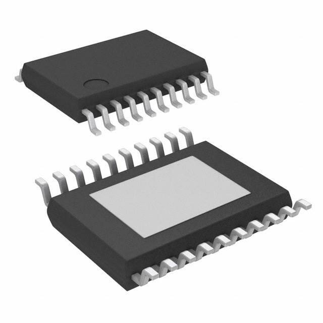
PWP PACKAGE
(TOP VIEW)
1
2
3
4
5
6
7
8
9
10
GND
SYNC
ENABLE
FB
OUT
C1+
IN
C1−
PGND
PGND
20
19
18
17
16
15
14
13
12
11
GND
3V8
COM
SKIP
OUT
C2+
IN
C2−
PGND
PGND
Thermal
Pad
Figure 2. Bottom View of PWP Package,
Showing the Thermal Pad
AVAILABLE OPTIONS
PACKAGE
TSSOP†
(PWP)
TPS60101PWP
† This package is available taped and reeled. To order this packaging
option, add an R suffix to the part number (e.g., TPS60101PWPR).
Terminal Functions
TERMINAL
NAME
NO.
I/O
DESCRIPTION
I
Mode selection. When 3V8 is logic low the charge pump operates in the regulated 3.3-V mode. When 3V8 is
connected to IN the regulator operates in preregulated 3.8-V mode.
3V8
19
C1+
6
Positive terminal of the charge-pump capacitor C1F
C1−
8
Negative terminal of the charge-pump capacitor C1F
C2+
15
Positive terminal of the charge-pump capacitor C2F
C2−
13
COM
18
I
Mode selection.
When COM is logic low the charge pump operates in push-pull mode to minimize output ripple. When COM is
connected to IN the regulator operates in single-ended mode requiring only one flying capacitor.
ENABLE
3
I
ENABLE Input. The device turns off, the output disconnects from the input, and the supply current decreases to
0.05 µA when ENABLE is a logic low. ENABLE High may only be applied when VIN is inside the recommended
operating range.
FB
4
I
FEEDBACK input. Connect FB to OUT as close to the load as possible to achieve best regulation. Resistive divider
is on chip to match internal reference voltage of 1.22 V.
Negative terminal of the charge-pump capacitor C2F
GND
1, 20
GROUND. Analog ground for internal reference and control circuitry. Connect to PGND through a short trace.
IN
7, 14
I
Supply Input. Connect to an input supply in the 1.8-V to 3.6-V range. Bypass IN to GND with a (CO/2) µF capacitor.
Connect both INs through a short trace.
OUT
5, 16
O
Regulated power output. Connect both OUTs through a short trace and bypass OUT to GND with the output filter
capacitor CO. VO = 3.3 V when 3V8 = low and VO = 3.8 V when 3V8 = high.
PGND
9−12
PGND power ground. Charge-pump current flows through this pin. Connect all PGNDs together.
SKIP
17
I
Mode selection. When SKIP is logic low, the charge pump operates in constant-frequency mode. Output ripple
and noise are minimized in this mode. When SKIP is connect to IN, the device operates in pulse skip mode.
Quiescent current is lowest in this mode.
SYNC
2
I
Selection for external clock signal. Connect to GND to use the internally generated clock signal. Connect to IN
for external synchronization. In this case, the clock signal needs to be fed through 3V8 and the device operates
in the regulated 3.3-V mode.
2
POST OFFICE BOX 655303
• DALLAS, TEXAS 75265
���������
��
����
����� ������ ���������
���� � �
��
��
� ���������
SLVS214B − JUNE 1999 − REVISED AUGUST 2008
absolute maximum ratings (unless otherwise noted)†‡
Input voltage range, VI (IN, OUT, ENABLE, SKIP, COM, 3V8, FB, SYNC) . . . . . . . . . . . . . . . . −0.3 V to 5.5 V
Differential input voltage, VID (C1+, C2+ to GND) . . . . . . . . . . . . . . . . . . . . . . . . . . . . −0.3 V to (VOUT + 0.3 V)
Differential input voltage, VID (C1−, C2− to GND) . . . . . . . . . . . . . . . . . . . . . . . . . . . . . . −0.3 V to (VIN + 0.3 V)
Continuous total power dissipation . . . . . . . . . . . . . . . . . . . . . . . . . . . . . . . . . . . . See Dissipation Rating Tables
Continuous output current . . . . . . . . . . . . . . . . . . . . . . . . . . . . . . . . . . . . . . . . . . . . . . . . . . . . . . . . . . . . . . . . 150 mA
Storage temperature range, Tstg . . . . . . . . . . . . . . . . . . . . . . . . . . . . . . . . . . . . . . . . . . . . . . . . . . . −55°C to 150°C
Lead temperature 1,6 mm (1/16 inch) from case for 10s . . . . . . . . . . . . . . . . . . . . . . . . . . . . . . . . . . . . . . . 260°C
Maximum junction temperature, TJ . . . . . . . . . . . . . . . . . . . . . . . . . . . . . . . . . . . . . . . . . . . . . . . . . . . . . . . . . 150°C
† Stresses beyond those listed under “absolute maximum ratings” may cause permanent damage to the device. These are stress ratings only, and
functional operation of the device at these or any other conditions beyond those indicated under “recommended operating conditions” is not
implied. Exposure to absolute-maximum-rated conditions for extended periods may affect device reliability.
‡ VENABLE, VSKIP, VCOM, V3V8 and VSYNC can exceed VIN up to the maximum rated voltage without increasing the leakage current drawn by these
mode select inputs.
DISSIPATION RATING TABLE 1 − FREE-AIR TEMPERATURE (see Figure 3)
PACKAGE
TA ≤ 25°C
25 C
POWER RATING
DERATING FACTOR
ABOVE TA = 25°C
70°C
TA = 70
C
POWER RATING
85°C
TA = 85
C
POWER RATING
PWP
700 mW
5.6 mW/°C
448 mW
364 mW
DISSIPATION RATING TABLE 2 − CASE TEMPERATURE (see Figure 4)
PACKAGE
TC ≤ 62.5
62.5°C
C
POWER RATING
DERATING FACTOR
ABOVE TC = 62.5°C
TC = 70
70°C
C
POWER RATING
TC = 85
85°C
C
POWER RATING
PWP
25 W
285.7 mW/°C
22.9 W
18.5 W
DISSIPATION DERATING CURVE§
vs
FREE-AIR TEMPERATURE
MAXIMUM CONTINUOUS DISSIPATION§
vs
CASE TEMPERATURE
30
PD − Maximum Continuous Dissipation − W
PD − Maximum Continuous Dissipation − mW
1400
1200
1000
800
PWP Package
RθJA = 178°C/W
600
400
200
0
25
50
75
100
125
150
TA − Free-Air Temperature − °C
25
20
PWP Package
15
10
Measured with the exposed thermal pad
coupled to an infinite heat sink with a
thermally conductive compound (the
thermal conductivity of the compound
is 0.815 W/m ⋅ °C). The RθJC is 3.5°C/W.
5
0
25
Figure 3
50
75
100
125
TC − Case Temperature − °C
150
Figure 4
§ Dissipation rating tables and figures are provided for maintenance of junction temperature at or below absolute maximum temperature of 150°C.
It is recommended not to exceed a junction temperature of 125°C.
POST OFFICE BOX 655303
• DALLAS, TEXAS 75265
3
���������
��
����
����� ������ ���������
���� � �
��
��
� ���������
SLVS214B − JUNE 1999 − REVISED AUGUST 2008
electrical characteristics at CIN = 10 µF, C1F = C2F = 2.2 µF†, CO = 22 µF, TC = −40°C to 85°C,
VIN = 2 V, VFB = VO, VENABLE = VIN, VSKIP = VIN or 0 V and VCOM = V3V8 = VSYNC = 0 V (unless otherwise
noted)
PARAMETER
TEST CONDITIONS
VIN
Input voltage
VIN(UV)
IO(MAX)
Input undervoltage lockout threshold
MIN
TYP
1.8
1.6
Maximum output current
MAX
3.6
V
1.8
V
100
mA
1.8 V < VIN < 2 V,
VO(Start-Up) = 3.3 V,
0 < IO < 50 mA,
TC = 25°C
3.17
3.3
3.43
2 V < VIN < 3.3 V,
0 < IO < 100 mA
3.17
3.3
3.43
3.3 V < VIN < 3.6 V,
0 < IO < 100 mA
3.17
3.47
Output leakage current
IO = 100 mA,
VIN = 2.4 V,
VSKIP = 0 V
VENABLE = 0 V
3.3
5‡
Quiescent current
(no-load input current)
VSKIP = VIN = 2.4 V
VSKIP = 0 V,
VIN = 2.4 V
IDD(SDN)
fOSC(int)
Shutdown supply current
VIN = 2.4 V,
VIN = 2.4 V
VENABLE = 0 V
fOSC(ext)
External clock frequency
External clock duty cycle
VSYNC = VIN,
VSYNC = VIN,
VIN = 1.8V to 3.6 V
VIN = 1.8V to 3.6 V
Efficiency
IO = 50 mA
VINL
Input voltage low,
ENABLE, SKIP, COM, 3V8, SYNC
VIN = 1.8 V
VINH
Input voltage high,
ENABLE, SKIP, COM, 3V8, SYNC
VIN = 3.6 V
II(LEAK)
Input leakage current,
ENABLE, SKIP, COM, 3V8, SYNC
VENABLE = VSKIP = VCOM = V3V8 =
VSYNC = VGND or VIN
Output load regulation
VO = 3.3 V,
TC = 25°C
1 mA < IO < 100 mA
Output line regulation
2 V < VIN < 3.3 V,
IO = 50 mA,
VO = 3.3 V,
TC = 25°C
Short circuit current
VIN = 2.4 V
TC = 25°C
VO = 0 V,
VO
VO(RIP)
IO(LEAK)
IQ
Output voltage
Output voltage ripple
Internal switching frequency
50
POST OFFICE BOX 655303
V
1
mVPP
µA
90
µA
1.5
mA
0.05
1
µA
200
300
400
kHz
400
600
800
kHz
20%
80%
80%
0.3 ×
VIN
0.7 ×
VIN
† Use only ceramic capacitors with X5R or X7R dielectric as flying capacitors.
‡ Achieved with CO = 22 µF X5R dielectric ceramic capacitor
4
UNIT
• DALLAS, TEXAS 75265
V
V
0.01
0.004
0.1
µA
%/mA
0.6
%/V
125
mA
���������
��
����
����� ������ ���������
���� � �
��
��
� ���������
SLVS214B − JUNE 1999 − REVISED AUGUST 2008
electrical characteristics for preregulated 3.8-V Mode (V(3V8) = VIN), at CIN = 10 µF,
C1F = C2F = 2.2 µF†, CO = 22 µF, TC = −40°C to 85°C, VIN = 2.4 V, VFB = VO, VENABLE = VIN,
VSKIP = VIN or 0 V and VCOM = VSYNC = 0 V (unless otherwise noted)
PARAMETER
TEST CONDITIONS
MIN
VIN
Input voltage
2.2
IO(MAX)
VO
Maximum output current
100
Output voltage
2.2 V < VIN < 3.6 V,
IO(LEAK)
Output leakage current
VENABLE = 0 V
VSKIP = VIN
IQ
IDD(SDN)
fOSC
Quiescent current
(no-load input current)
Shutdown supply current
0 < IO < 100 mA
3.6
VSKIP = 0 V
VENABLE = 0 V
Internal switching frequency
200
Short circuit current
VO = 0 V,
† Use only ceramic capacitors with X5R or X7R dielectric as flying capacitors.
POST OFFICE BOX 655303
TC = 25°C
• DALLAS, TEXAS 75265
TYP
MAX
3.6
UNIT
V
mA
3.8
4
V
1
µA
60
µA
2
mA
0.05
1
µA
300
400
kHz
125
mA
5
���������
��
����
����� ������ ���������
���� � �
��
��
� ���������
SLVS214B − JUNE 1999 − REVISED AUGUST 2008
TYPICAL CHARACTERISTICS†
EFFICIENCY
vs
OUTPUT CURRENT (VO = 3.3 V)
EFFICIENCY
vs
OUTPUT CURRENT (VO = 3.3 V)
100
100
VIN = 1.8 V
90
V(SKIP) = 0 V
V(3V8) = 0 V
90
VIN = 2 V
80
VIN = 2.4 V
60
50
40
50
40
30
20
20
10
V(SKIP) = VIN, V(3V8) = 0 V
1
100
10
VIN = 2.7 V
60
30
10
VIN = 2.4 V
70
VIN = 2.7 V
Efficiency − %
Efficiency − %
VIN = 2 V
80
70
0
0.1
0
1000
1
Figure 6
EFFICIENCY
vs
OUTPUT CURRENT (VO = 3.8 V)
EFFICIENCY
vs
OUTPUT CURRENT (VO = 3.8 V)
100
100
V(SKIP) = VIN
V(3V8) = VIN
VIN = 2.3 V
VIN = 2.3 V
80
VIN = 2.7 V
70
60
50
40
50
40
30
20
20
10
10
10
100
1000
VIN = 3 V
60
30
1
VIN = 2.7 V
70
VIN = 3 V
Efficiency − %
Efficiency − %
V(SKIP) = 0 V
V(3V8) = VIN
90
80
0
1
IO − Output Current − mA
10
Figure 8
† TC = 25°C, VCOM = VSYNC = 0 V, CIN = 10 µF, C1F = C2F = 2.2 µF, CO = 22 µF, unless otherwise noted
POST OFFICE BOX 655303
100
IO − Output Current − mA
Figure 7
6
1000
IO − Output Current − mA
Figure 5
0
0.1
100
10
IO − Output Current − mA
90
VIN = 1.8 V
• DALLAS, TEXAS 75265
1000
���������
��
����
����� ������ ���������
���� � �
��
��
� ���������
SLVS214B − JUNE 1999 − REVISED AUGUST 2008
TYPICAL CHARACTERISTICS†
QUIESCENT SUPPLY CURRENT
vs
INPUT VOLTAGE
QUIESCENT SUPPLY CURRENT
vs
INPUT VOLTAGE
2
V(SKIP) = VIN
V(3V8) = 0 V
55
I Q − Quiescent Supply Current − mA
I Q − Quiescent Supply Current − µ A
60
50
45
40
35
30
25
1.5
2
2.5
3.5
3
V(SKIP) = 0 V
V(3V8) = 0 V
1.75
1.5
1.25
1
1.5
4
VIN − Input Voltage − V
4
OUTPUT VOLTAGE
vs
OUTPUT CURRENT
3.6
4.1
V(SKIP) = VIN or 0 V
V(3V8) = 0 V
V(SKIP) = VIN or 0 V
V(3V8) = VIN
4
VIN = 3.6 V
VIN = 2.7 V
VIN = 2.4 V
VO − Output Voltage − V
VO − Output Voltage − V
3.5
3
Figure 10
OUTPUT VOLTAGE
vs
OUTPUT CURRENT
3.4
2.5
VIN − Input Voltage − V
Figure 9
3.5
2
3.3
VIN = 2 V
3.2
VIN = 1.8 V
3.1
VIN = 3.6 V
VIN = 2.7 V
VIN = 2.4 V
3.9
3.8
3.7
3.6
3
1
10
100
1000
3.5
1
IO − Output Current − mA
10
100
1000
IO − Output Current − mA
Figure 11
Figure 12
† TC = 25°C, VCOM = VSYNC = 0 V, CIN = 10 µF, C1F = C2F = 2.2 µF, CO = 22 µF, unless otherwise noted
POST OFFICE BOX 655303
• DALLAS, TEXAS 75265
7
���������
��
����
����� ������ ���������
���� � �
��
��
� ���������
SLVS214B − JUNE 1999 − REVISED AUGUST 2008
TYPICAL CHARACTERISTICS†
OUTPUT VOLTAGE
vs
INPUT VOLTAGE
OUTPUT VOLTAGE
vs
INPUT VOLTAGE
3.5
3.45
3.4
3.35
3.3
3.25
3.2
3.15
3.8
3.7
3.4
3.3
3.05
3.1
2.5
3.5
3
IO = 100 mA
3.5
3.2
2
IO = 10 mA
3.6
3.1
3
1.5
V(SKIP) = VIN or 0 V
V(3V8) = VIN
3.9
VO − Output Voltage − V
VO − Output Voltage − V
3.10
V(SKIP) = VIN or 0 V
V(3V8) = 0 V
IO = 1 mA to 100 mA
3
1.5
4
2
VIN − Input Voltage − V
2.5
4
Figure 14
Figure 13
OUTPUT VOLTAGE
vs
TIME
OUTPUT VOLTAGE
vs
TIME
3.36
3.38
V(SKIP) = 0 V
V(3V8) = 0 V
VIN = 2.4 V
IO = 50 mA
CO = 22 µF (X5R ceramic)
Pulse-Skip Mode
Constant
Frequency
Mode
VO − Output Voltage − V
3.35
VO − Output Voltage − V
3.5
3
VIN − Input Voltage − V
3.34
3.33
Less than
5 mVpp
3.32
3.36
3.34
3.32
V(SKIP) = VIN
V(3V8) = 0 V
IO = 100 mA
3.31
3.30
0
1
2
3
4
5
6
7
8
3.3
−5
t − Time − µs
0
5
10
t − Time − µs
Figure 15
Figure 16
† TC = 25°C, VCOM = VSYNC = 0 V, CIN = 10 µF, C1F = C2F = 2.2 µF, CO = 22 µF, unless otherwise noted
8
POST OFFICE BOX 655303
• DALLAS, TEXAS 75265
15
20
25
���������
��
����
����� ������ ���������
���� � �
��
��
� ���������
SLVS214B − JUNE 1999 − REVISED AUGUST 2008
TYPICAL CHARACTERISTICS†
V(SKIP) = 0 V
V(3V8) = 0 V
V(IN) = 2.7 V
IO = 10 mA to 200 mA
3.35
LOAD TRANSIENT RESPONSE
VO − Output Voltage − V
VO − Output Voltage − V
LOAD TRANSIENT RESPONSE
3.36
Constant
Frequency
Mode
3.34
3.33
I O − Output Current − mA
I O − Output Current − mA
3.32
300
200
100
0
0
2
4
6
8
10
12
14
16
18
3.39
V(SKIP) = VIN
V(3V8) = 0 V
V(IN) = 2.7 V
IO = 10 mA to 200 mA
3.37
3.35
3.33
3.31
300
200
100
0
20
0
2
4
6
12
14
16
18
20
LINE TRANSIENT RESPONSE
VO − Output Voltage − V
LINE TRANSIENT RESPONSE
VO − Output Voltage − V
10
Figure 18
Figure 17
3.39
V(SKIP) = 0 V
V(3V8) = 0 V
IO = 100 mA
Constant
Frequency
Mode
3.35
3.33
3.45
V(SKIP) = VIN
V(3V8) = 0 V
IO = 100 mA
3.4
Pulse-Skip Mode
3.35
3.3
3.25
3
2.5
2
1.5
0
1
2
3
4
5
6
7
8
9
10
V IN − Input Voltage − V
3.31
V IN − Input Voltage − V
8
t − Time − ms
t − Time − ms
3.37
Pulse-Skip Mode
3
2.5
2
1.5
0
1
2
3
4
5
6
7
8
9
10
t − Time − ms
t − Time − ms
Figure 19
Figure 20
† TC = 25°C, VCOM = VSYNC = 0 V, CIN = 10 µF, C1F = C2F = 2.2 µF, CO = 22 µF, unless otherwise noted
POST OFFICE BOX 655303
• DALLAS, TEXAS 75265
9
���������
��
����
����� ������ ���������
���� � �
��
��
� ���������
SLVS214B − JUNE 1999 − REVISED AUGUST 2008
TYPICAL CHARACTERISTICS†
FREQUENCY SPECTRUM
CONSTANT FREQUENCY MODE‡
FREQUENCY SPECTRUM
PULSE-SKIP MODE‡
90
100
V(SKIP) = 0 V
V(3V8) = 0 V
VIN = 2.4 V
IO = 100 mA
RBW = 300 Hz
80
80
60
Output − dB µ V
Output − dB µ V
70
V(SKIP) = VIN
V(3V8) = 0 V
VIN = 2.4 V
IO = 100 mA
RBW = 300 Hz
50
40
60
40
30
20
20
10
0
0
0
2.5
7.5
5
10
0
2.5
Figure 21
FREQUENCY SPECTRUM
PULSE-SKIP MODE‡
90
90
V(SKIP) = 0 V
V(3V8) = 0 V
VIN = 2.4 V
IO = 10 mA
80
70
V(SKIP) = VIN
V(3V8) = 0 V
VIN = 2.4 V
IO = 10 mA
80
70
60
Output − dB µ V
Output − dB µ V
10
Figure 22
FREQUENCY SPECTRUM
CONSTANT FREQUENCY MODE‡
50
40
60
50
40
30
30
20
20
10
10
0
0
0
2.5
5
7.5
10
0
f − Frequency − MHz
2.5
5
f − Frequency − MHz
Figure 23
Figure 24
† TC = 25°C, VCOM = VSYNC = 0 V, CIN = 10 µF, C1F = C2F = 2.2 µF, CO = 22 µF, unless otherwise noted
‡ Test circuit: TPS60100EVM−131 with TPS60101
10
7.5
5
f − Frequency − MHz
f − Frequency − MHz
POST OFFICE BOX 655303
• DALLAS, TEXAS 75265
7.5
10
���������
��
����
����� ������ ���������
���� � �
��
��
� ���������
SLVS214B − JUNE 1999 − REVISED AUGUST 2008
TYPICAL CHARACTERISTICS†
EFFICIENCY
vs
INPUT VOLTAGE
EFFICIENCY
vs
INPUT VOLTAGE
100
100
V(3V8) = 0 V
IO = 100 mA
80
80
70
70
Skip = High
60
Skip = Low
50
40
Skip = Low
50
40
30
20
20
10
10
2
2.5
3
3.5
Skip = High
60
30
0
1.5
V(3V8) = VIN
IO = 100 mA
90
Efficiency − %
Efficiency − %
90
0
1.5
4
2
2.5
Figure 25
START-UP TIMING
4
R0 = 33 Ω
VIN = 2.4 V
V(3V8) = 0 V
3.5
2
Enable
OUTPUT
1.5
1
0.5
2.5
2
OUTPUT
Enable
1.5
1
0.5
0
−0.5
−100
R0 = 38 Ω
VIN = 2.4 V
V(3V8) = VIN
3
2.5
VO − Output Voltage − V
VO − Output Voltage − V
3
4
Figure 26
START-UP TIMING
3.5
3.5
3
VIN − Input Voltage − V
VIN − Input Voltage − V
0
0
100
200
300
400
500
−0.5
−100
0
100
200
300
400
500
t − Time −µs
t − Time −µs
Figure 27
Figure 28
† TC = 25°C, VCOM = VSYNC = 0 V, CIN = 10 µF, C1F = C2F = 2.2 µF, CO = 22 µF, unless otherwise noted
POST OFFICE BOX 655303
• DALLAS, TEXAS 75265
11
���������
��
����
����� ������ ���������
���� � �
��
��
� ���������
SLVS214B − JUNE 1999 − REVISED AUGUST 2008
detailed description
operating principle
The TPS60101 charge pump provides a regulated 3.3-V output from a 1.8-V to 3.6-V input. It delivers a
maximum load current of 100 mA. Designed specifically for space critical battery powered applications, the
complete charge pump circuit requires only four external capacitors. The circuit can be optimized for highest
efficiency at light loads or lowest output noise. The TPS60101 consists of an oscillator, a 1.22-V bandgap
reference, an internal resistive feedback circuit, an error amplifier, high current MOSFET switches, a
shutdown/start-up circuit, and a control circuit (Figure 29)
CHARGE PUMP 1
IN
0°
T11
OSCILLATOR
T12
180°
C1+
C1F
T13
SKIP
C1−
T14
OUT
COM
3V8
PGND
CONTROL
CIRCUIT
SYNC
FB
−
CHARGE PUMP 2
IN
+
T21
VREF +
−
T22
C2+
ENABLE
SHUTDOWN/
START-UP
CONTROL
−
+
T23
+
−
T24
C2F
C2−
OUT
0.8 × VIN
PGND
GND
Figure 29. Functional Block Diagram TPS60101
The oscillator runs at a 50% duty cycle. The device consists of two single-ended charge pumps which operate
with 180° phase shift. Each single ended charge pump transfers charge into its transfer capacitor (CxF) in one
half of the period. During the other half of the period (transfer phase), CxF is placed in series with the input to
transfer its charge to CO. While one single-ended charge pump is in the charge phase, the other one is in the
transfer phase. This operation guarantees an almost constant output current which ensures a low output ripple.
If the clock were to run continuously, this process would eventually generate an output voltage equal to two times
the input voltage (hence the name doubler). In order to provide a regulated fixed output voltage of 3.3 V, the
TPS60101 uses either pulse-skip mode or constant-frequency mode. Pulse-skip mode and constant-frequency
mode are externally selected via the SKIP input pin.
12
POST OFFICE BOX 655303
• DALLAS, TEXAS 75265
���������
��
����
����� ������ ���������
���� � �
��
��
� ���������
SLVS214B − JUNE 1999 − REVISED AUGUST 2008
detailed description (continued)
start-up procedure
During start-up, i.e. when ENABLE is set from logic low to logic high, the switches T12 and T14 (charge pump
1), and the switches T22 and T24 (charge pump 2) are conducting to charge up the output capacitor until the
output voltage VO reaches 0.8×VIN. When the start-up comparator detects this limit, the IC begins to operate
in the mode selected with SKIP, COM and 3V8. This start-up charging of the output capacitor guarantees a short
start-up time and eliminates the need for a Schottky diode between IN and OUT.
pulse-skip mode
In pulse-skip mode (SKIP = high), the error amplifier disables switching of the power stages when it detects an
output higher than 3.3 V. The oscillator halts. The IC then skips switching cycles until the output voltage drops
below 3.3 V. Then the error amplifier reactivates the oscillator and switching of the power stages starts again.
The pulse-skip regulation mode minimizes operating current because it does not switch continuously and
deactivates all functions except bandgap reference and error amplifier when the output is higher than 3.3 V.
When switching is disabled from the error amplifier, the load is also isolated from the input. SKIP is a logic input
and should not remain floating. The typical operating circuit of the TPS60101 in pulse skip mode is shown in
Figure 1.
constant-frequency mode
When SKIP is low, the charge pump runs continuously at the frequency fOSC. The control circuit, fed from the
error amplifier, controls the charge on C1F and C2F by driving the gates of the FETs T12/T13 and T22/T23,
respectively. When the output voltage falls, the gate drive increases, resulting in a larger voltage across C1F
and C2F. This regulation scheme minimizes output ripple. Since the device switches continuously, the output
noise contains well-defined frequency components, and the circuit requires smaller external capacitors for a
given output ripple. However, constant-frequency mode, due to higher operating current, is less efficient at light
loads than pulse-skip mode.
SKIP COM 3V8
INPUT
1.8 V to 3.6 V
CIN
4.7 µF
IN
IN
+
C1F
1 µF
C1+
C2+
C1−
C2−
ENABLE
OFF/ON
OUTPUT
3.3 V 100 mA
OUT
OUT
TPS60101 FB
+
CO = 22 µF
C2F
1 µF
SYNC
PGND GND
Figure 30. Typical Operating Circuit TPS60101 in Constant Frequency Mode
Table 1. Tradeoffs Between Operating Modes
FEATURE
PULSE-SKIP MODE
(SKIP = High)
Best light-load efficiency
CONSTANT-FREQUENCY MODE
(SKIP = Low)
X
Smallest external component size for a given output ripple
X
Output ripple amplitude
Small amplitude
Very small amplitude
Output ripple frequency
Variable
Constant
Very good
Good
Load regulation
NOTE: Even in pulse-skip mode the output ripple amplitude is small if the push-pull operating mode is selected via COM.
POST OFFICE BOX 655303
• DALLAS, TEXAS 75265
13
���������
��
����
����� ������ ���������
���� � �
��
��
� ���������
SLVS214B − JUNE 1999 − REVISED AUGUST 2008
detailed description (continued)
push-pull operating mode
In push-pull operating mode (COM = low), the two single-ended charge pumps operate with 180° phase shift.
The oscillator signal has a 50% duty cycle. Each single-ended charge pump transfers charge into its transfer
capacitor (CxF) in one-half of the period. During the other half of the period (transfer phase), CxF is placed in
series with the input to transfer its charge to CO. While one single-ended charge pump is in the charge phase,
the other one is in the transfer phase. This operation guarantees an almost constant output current which
ensures a low output ripple. COM is a logic input and should not remain floating. The typical operating circuit
of the TPS60101 in push-pull mode is shown in Figure 1 and Figure 30.
single-ended operating mode
When COM is high, the device runs in single-ended operating mode. The two single-ended charge pumps
operate in parallel without phase shift. They transfer charge into the transfer capacitor (CF) in one half of the
period. During the other half of the period (transfer phase), CF is placed in series with the input to transfer its
charge to CO. In single-ended operating mode only one transfer capacitor (CF = C1F + C2F) is required, resulting
in less board space.
SKIP COM 3V8
INPUT
1.8 V to 3.6 V
IN
IN
CIN
4.7 µF
+
OUT
OUT
TPS60101 FB
C1+
C2+
C1−
C2−
ENABLE
OFF/ON
OUTPUT
3.3 V 100 mA
+
CO = 10 µF
SYNC
PGND GND
CF = 2.2 µF
Figure 31. Typical Operating Circuit TPS60101 in Single-Ended Operating Mode
Table 2. Tradeoffs Between Operating Modes
FEATURE
Output ripple amplitude
PUSH-PULL MODE
(COM = Low)
SINGLE-ENDED MODE
(COM = High)
Small amplitude
Large amplitude
Smallest board space
X
regulated 3.3 V operating mode
In regulated 3.3-V operating mode (3V8 = low) the device provides a regulated 3.3-V output from a1.8-V to 3.6-V
input. 3V8 is a logic input and should not remain floating. The typical operating circuit of the TPS60101 in (3.3
V) regulated mode is shown in Figure 1 and Figure 30.
pre-regulated 3.8 V operating mode
When 3V8 is high, the device provides a preregulated 3.8-V output from a 2.2-V to 3.6-V input. This mode should
be used if a tighter output voltage tolerance is a major concern. In this case the charge pump generates the input
voltage for a low-dropout regulator.
14
POST OFFICE BOX 655303
• DALLAS, TEXAS 75265
���������
��
����
����� ������ ���������
���� � �
��
��
� ���������
SLVS214B − JUNE 1999 − REVISED AUGUST 2008
detailed description (continued)
shutdown
Driving ENABLE low places the device in shutdown mode. This disables all switches, the oscillator, and control
logic. The device typically draws 0.05-µA (1-µA max) of supply current in this mode. Leakage current drawn from
the output is as low as 1 µA max. The device exits shutdown once ENABLE is set high level. The typical no-load
shutdown exit time is 10 µs. When the device is in shutdown, the load is isolated from the input and the output
is high impedance.
external clock signal
If the device operates at a user defined frequency, an external clock signal can be used. Therefore, SYNC needs
to be connected to IN and the external oscillator signal can drive 3V8. The maximum external frequency is
limited to 800 kHz. The switching frequency of the converter is half of the external oscillator frequency. It is
recommended to operate the charge pump in constant-frequency mode if an external clock signal is used so
that the output noise contains only well-defined frequency components.
External Clock
SKIP COM 3V8
INPUT
1.8 V to 3.6 V
IN
IN
CIN
4.7 µF
+
C1F
1 µF
C1+
C2+
C1−
C2−
ENABLE
OFF/ON
OUTPUT
3.3 V 100 mA
OUT
OUT
TPS60101 FB
+
CO = 22 µF
C2F
1 µF
SYNC
PGND GND
Figure 32. Typical Operating Circuit TPS60101 With External Synchronization
undervoltage lockout
The TPS60101 has an undervoltage lockout feature that deactivates the device and places it in shutdown mode
when the input voltage falls below 1.6 V.
POST OFFICE BOX 655303
• DALLAS, TEXAS 75265
15
���������
��
����
����� ������ ���������
���� � �
��
��
� ���������
SLVS214B − JUNE 1999 − REVISED AUGUST 2008
APPLICATION INFORMATION
capacitor selection
The TPS60101 requires only four external capacitors as shown in the basic application circuit. Their values are
closely linked to the output current capacity, output noise requirements, and mode of operation. Generally, the
transfer capacitors (CxF) will be the smallest.
The input capacitor improves system efficiency by reducing the input impedance and stabilizes the input current.
CIN is recommended to be about two to four times as large as CxF.
The output capacitor (CO) can be selected from 5-times to 50-times larger than CxF, depending on the mode
of operation and ripple tolerance†. Tables 3 and 4 show capacitor values recommended for low
quiescent-current operation (pulse-skip mode) and for low output voltage ripple operation (constant-frequency
mode). A recommendation is given for smallest size.
Table 3. Recommended Capacitor Values for Low Quiescent-Current Operation†
(pulse-skip mode)
VIN
[V]
CIN
[µF]
IO [mA]
TANTALUM
2.4
50
2.4
50
2.4
100
2.4
100
CO
[µF]
CxF
[µF]
CERAMIC
TANTALUM
4.7
1
4.7 (X7R)
CERAMIC
10
135
1
4.7
1
4.7 (X7R)
OUTPUT
VOLTAGE
RIPPLE VPP
[mV]
10 (X5R)
10
125
70
1
10 (X5R)
65
† All measurements are done with additional 1-µF X7R ceramic capacitors at input and output.
Table 4. Recommended Capacitor Values for Low Output Voltage Ripple Operation†
(constant-frequency mode)
VIN
[V]
CIN
[µF]
IO
[mA]
TANTALUM
2.4
50
2.4
50
2.4
100
2.4
100
CO
[µF]
CxF
[µF]
CERAMIC
4.7
TANTALUM
1
4.7 (X7R)
4.7
22
1
1
4.7 (X7R)
CERAMIC
5
22 (X5R)
22
1
16
POST OFFICE BOX 655303
• DALLAS, TEXAS 75265
3
10
22 (X5R)
† All measurements are done with additional 1-µF X7R ceramic capacitors at input and output.
† In constant-frequency mode always select CO ≥ 22 µF
OUTPUT
VOLTAGE
RIPPLE VPP
[mV]
5
���������
��
����
����� ������ ���������
���� � �
��
��
� ���������
SLVS214B − JUNE 1999 − REVISED AUGUST 2008
APPLICATION INFORMATION
For the TPS60101, the smallest board space size can be achieved using Sprague’s 595D-series tantalum
capacitors for input and output. However, with the trend towards high capacitance ceramic capacitors in smaller
size packages, these type of capacitors might become competitive in size soon.
Table 5. Recommended Capacitors
MANUFACTURER
PART NUMBER
CAPACITANCE
TYPE
Taiyo Yuden
LMK212BJ105KG−T
LMK212BJ225MG−T
LMK316BJ475KL−T
JMK316BJ106ML−T
LMK432BJ226MM−T
1 µF
2.2 µF
4.7 µF
10 µF
22 µF
Ceramic
Ceramic
Ceramic
Ceramic
Ceramic
AVX
0805ZC105KAT2A
1206ZC225KAT2A
TPSC475035R0600
TPSC106025R0500
TPSC226016R0375
1 µF
2.2 µF
4.7 µF
10 µF
22 µF
Ceramic
Ceramic
Tantalum
Tantalum
Tantalum
Sprague
595D475X0016A2T
595D106X0010A2T
595D226X06R3A2T
595D226X06R3B2T
595D226X0020C2T
4.7 µF
10 µF
22 µF
22 µF
22 µF
Tantalum
Tantalum
Tantalum
Tantalum
Tantalum
Kemet
T494B475M010AS
T494C106M010AS
T494C226M010AS
4.7 µF
10 µF
22 µF
Tantalum
Tantalum
Tantalum
Table 6 lists the manufacturers of recommended capacitors. In most applications surface-mount tantalum
capacitors will be the right choice. However, ceramic capacitors will provide the lowest output voltage ripple due
to their typically lower ESR.
Table 6. Recommended Capacitor Manufacturers
MANUFACTURER
CAPACITOR TYPE
INTERNET
Taiyo Yuden
X7R/X5R ceramic
www.t−yuden.com
AVX
X7R/X5R ceramic
TPS−series tantalum
www.avxcorp.com
Sprague
595D−series tantalum
593D−series tantalum
www.vishay.com
Kemet
T494−series tantalum
www.kemet.com
power dissipation
The power dissipated in the TPS60101 depends on output current and is approximated by:
P DISS + I O
ǒ2 VIN * VOǓ for I Q tt
IO
PDISS must be less than that allowed by the package rating. See the ratings for 20-PowerPAD package
power-dissipation limits and deratings.
POST OFFICE BOX 655303
• DALLAS, TEXAS 75265
17
���������
��
����
����� ������ ���������
���� � �
��
��
� ���������
SLVS214B − JUNE 1999 − REVISED AUGUST 2008
APPLICATION INFORMATION
layout
All capacitors should be soldered in close proximity to the IC. A PCB layout proposal for a two-layer board is
given in Figure 33. Care has been taken to connect both single-ended charge pumps symmetrically to the load
to achive optimized output voltage ripple performance. The proposed layout also provides improved thermal
performance as the exposed leadframe is soldered to the PCB. The bottom layer of the PCB is a ground plain
only. All ground areas on the PCB should be connected. Connect ground areas on top layer to the bottom layer
via through hole connections.
OUT
GND
GND
3V8
SYNC
COM
ENABLE
SKIP
C1+
C2+
GND
C1−
C2−
GND
GND
IN
Figure 33. Recommended PCB Layout for TPS60101 (top view)
The evaluation module designed for the TPS60100 can, with slight modifications, be used for evaluation of the
TPS60101. The EVM can be ordered under literature code SLVP131 or under product code
TPS60100EVM−131.
18
POST OFFICE BOX 655303
• DALLAS, TEXAS 75265
���������
��
����
����� ������ ���������
���� � �
��
��
� ���������
SLVS214B − JUNE 1999 − REVISED AUGUST 2008
APPLICATION INFORMATION
applications proposals
TPS60101 with LC output filter for ultra low ripple
For applications where extremely low output ripple is required, a small LC filter is recommended. This is shown
in Figure 34. The addition of a small inductor and filter capacitor will reduce the output ripple well below what
could be achieved with capacitors alone. The corner frequency of 500 kHz was chosen above the 300 kHz
switching frequency to avoid loop stability issues in case the feedback is taken from the output of the LC filter.
Leaving the feedback (FB) connection point before the LC filter, the filter capacitance value can be increased
to achieve even higher ripple attenuation without affecting stability margin.
0.1 µH
SKIP COM 3V8
INPUT
1.8 V to 3.6 V
CIN
4.7 µF
IN
IN
+
C1F
1 µF
+
CO = 22 µF
1 µF
OUT
OUT
TPS60101 FB
C1+
C2+
C1−
C2−
ENABLE
OFF/ON
+
OUTPUT
3.3 V 100 mA
C2F
1 µF
SYNC
PGND GND
Figure 34. TPS60101 With LC Filter for Ultra Low Output Ripple Applications
related information
application reports
For more application information see:
D PowerPAD Application Report (Literature Number: SLMA002)
D TPS6010x/TPS6011x Charge Pump Application Report (Literature Number: SLVA070)
device family products
Other devices in this family are:
PART NUMBER
LITERATURE
NUMBER
TPS60100
SLVS213
Regulated 3.3-V, 200-mA Low-Noise Charge Pump DC/DC Converter
TPS60110
SLVS215
Regulated 5-V, 300-mA Low-Noise Charge Pump DC/DC Converter
TPS60111
SLVS216
Regulated 5-V, 150-mA Low-Noise Charge Pump DC/DC Converter
DESCRIPTION
POST OFFICE BOX 655303
• DALLAS, TEXAS 75265
19
�PACKAGE OPTION ADDENDUM
www.ti.com
10-Dec-2020
PACKAGING INFORMATION
Orderable Device
Status
(1)
Package Type Package Pins Package
Drawing
Qty
Eco Plan
(2)
Lead finish/
Ball material
MSL Peak Temp
Op Temp (°C)
Device Marking
(3)
(4/5)
(6)
TPS60101PWP
ACTIVE
HTSSOP
PWP
20
70
RoHS & Green
NIPDAU
Level-2-260C-1 YEAR
-40 to 85
TPS60101
(1)
The marketing status values are defined as follows:
ACTIVE: Product device recommended for new designs.
LIFEBUY: TI has announced that the device will be discontinued, and a lifetime-buy period is in effect.
NRND: Not recommended for new designs. Device is in production to support existing customers, but TI does not recommend using this part in a new design.
PREVIEW: Device has been announced but is not in production. Samples may or may not be available.
OBSOLETE: TI has discontinued the production of the device.
(2)
RoHS: TI defines "RoHS" to mean semiconductor products that are compliant with the current EU RoHS requirements for all 10 RoHS substances, including the requirement that RoHS substance
do not exceed 0.1% by weight in homogeneous materials. Where designed to be soldered at high temperatures, "RoHS" products are suitable for use in specified lead-free processes. TI may
reference these types of products as "Pb-Free".
RoHS Exempt: TI defines "RoHS Exempt" to mean products that contain lead but are compliant with EU RoHS pursuant to a specific EU RoHS exemption.
Green: TI defines "Green" to mean the content of Chlorine (Cl) and Bromine (Br) based flame retardants meet JS709B low halogen requirements of


 工商网监
湘ICP备2023018690号
工商网监
湘ICP备2023018690号
