Typical Size
6,4 mm X 9,7 mm
www.ti.com
TPS54974
SLVS458B – JANUARY 2003 – REVISED FEBRUARY 2005
DUAL INPUT BUS (2.5 V, 3.3 V) 9-A OUTPUT SYNCHRONOUS BUCK
PWM SWITCHER WITH INTEGRATED FETs (SWIFT™)
FEATURES
•
•
•
•
•
•
•
•
DESCRIPTION
Low Voltage Separate Power Bus
15-mΩ MOSFET Switches for High Efficiency
at 9-A Continuous Output
Adjustable Output Voltage
Externally Compensated With 1% Internal
Reference Accuracy
Fast Transient Response
Wide PWM Frequency: Adjustable 280 kHz to
700 kHz
Load Protected by Peak Current Limit and
Thermal Shutdown
Integrated Solution Reduces Board Area and
Total Cost
APPLICATIONS
•
•
•
•
As a member of the SWIFT™ family of dc/dc regulators, the TPS54974 low-input voltage, high-output
current synchronous buck PWM converter integrates
all required active components. Included on the
substrate with the listed features are a true,
high-performance, voltage error amplifier that enables
maximum performance under transient conditions
and flexibility in choosing the output filter L and C
components; an undervoltage-lockout circuit to prevent start-up until the VIN input voltage reaches 3 V;
an internally and externally set slow-start circuit to
limit in-rush currents; and a power-good output useful
for processor/logic reset, fault signaling, and supply
sequencing.
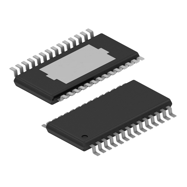
The TPS54974 is available in a thermally enhanced
28-pin TSSOP (PWP) PowerPAD™ package, which
eliminates bulky heatsinks.
Low-Voltage, High-Density Systems
With Power Distributed at 2.5 V,
3.3 V Available
Point-of-Load Regulation for
High-Performance
DSPs, FPGAs, ASICs, and
Microprocessors
Broadband, Networking, and Optical
Communications Infrastructure
Portable Computing/Notebook PCs
SIMPLIFIED SCHEMATIC
EFFICIENCY
vs
OUTPUT CURRENT
SIMPLIFIED SCHEMATIC
2.5 V or 3.3 V
Input1
100
PVIN
PH
Output
95
TPS54974
BOOT
PGND
3.3 V
VIN
85
Efficiency - %
Input2
90
COMP
VBIAS
AGND VSENSE
80
75
70
65
Compensation
Network
VIN = 3.3 V,
PVIN = 2.5 V,
VO = 1.8 V,
fs= 700 kHz
60
55
50
0
1
2
3
4
5
6
7
8
9
10
IO - Output Current - A
Please be aware that an important notice concerning availability, standard warranty, and use in critical applications of Texas
Instruments semiconductor products and disclaimers thereto appears at the end of this data sheet.
SWIFT, PowerPAD are trademarks of Texas Instruments.
PRODUCTION DATA information is current as of publication date.
Products conform to specifications per the terms of the Texas
Instruments standard warranty. Production processing does not
necessarily include testing of all parameters.
Copyright © 2003–2005, Texas Instruments Incorporated
�TPS54974
www.ti.com
SLVS458B – JANUARY 2003 – REVISED FEBRUARY 2005
These devices have limited built-in ESD protection. The leads should be shorted together or the device
placed in conductive foam during storage or handling to prevent electrostatic damage to the MOS gates.
ORDERING INFORMATION
(1)
TA
OUTPUT VOLTAGE
PACKAGE
PART NUMBER
–40°C to 85°C
Adjustable down to 0.9 V
Plastic HTSSOP (PWP) (1)
TPS54974PWP
The PWP package is also available taped and reeled. Add an R suffix to the device type (i.e., TPS54974PWPR). See the application
section of the data sheet for PowerPAD drawing and layout information.
ABSOLUTE MAXIMUM RATINGS
over operating free-air temperature range unless otherwise noted (1)
TPS54974
VI
Input voltage range
VO
Output voltage range
IO
Source current
IS
Sink current
Voltage differential
SS/ENA
–0.3 V to 7 V
RT
–0.3 V to 6 V
VSENSE
–0.3 V to 4 V
PVIN, VIN
–0.3 V to 4.5 V
BOOT
–0.3 V to 10 V
VBIAS, COMP, PWRGD
–0.3 V to 7 V
PH
–0.6 V to 6 V
PH
Internally limited
COMP, VBIAS
6 mA
PH
16 A
COMP
6 mA
SS/ENA, PWRGD
10 mA
AGND to PGND
±0.3 V
TJ
Operating virtual junction temperature range
–40°C to 125°C
Tstg
Storage temperature
–65°C to 150°C
Lead temperature 1,6 mm (1/16 inch) from case for 10 seconds
(1)
300°C
Stresses beyond those listed under "absolute maximum ratings" may cause permanent damage to the device. These are stress ratings
only, and functional operation of the device at these or any other conditions beyond those indicated under "recommended operating
conditions" is not implied. Exposure to absolute-maximum-rated conditions for extended periods may affect device reliability.
RECOMMENDED OPERATING CONDITIONS
MIN NOM MAX
VI
Input voltage, VIN
3
PVIN
Power input voltage
2.2
TJ
Operating junction temperature
–40
2.5
UNIT
4
V
4.0
V
125
°C
DISSIPATION RATINGS (1) (2)
(1)
(2)
(3)
2
PACKAGE
THERMAL IMPEDANCE
JUNCTION-TO-AMBIENT
TA = 25°C
POWER RATING
TA = 70°C
POWER RATING
TA = 85°C
POWER RATING
28-Pin PWP with solder
14.4°C/W
6.94 W (3)
3.81 W
2.77 W
28-Pin PWP without solder
27.9°C/W
3.58 W
1.97 W
1.43 W
For more information on the PWP package, see TI technical brief, literature number SLMA002.
Test board conditions:
a. 3-inch x 3-inch, 4 layers, thickness: 0.062-inch
b. 1.5-oz. copper traces located on the top of the PCB
c. 1.5-oz. copper ground plane on the bottom of the PCB
d. 0.5-oz. copper ground planes on the 2 internal layers
e. 12 thermal vias (see "Recommended Land Pattern" in applications section of this data sheet)
Maximum power dissipation may be limited by overcurrent protection.
�TPS54974
www.ti.com
SLVS458B – JANUARY 2003 – REVISED FEBRUARY 2005
ELECTRICAL CHARACTERISTICS
TJ = –40°C to 125°C, VIN = 3 V to 4 V, PVIN = 2.2 V to 2.8 V (unless otherwise noted)
PARAMETER
TEST CONDITIONS
MIN
TYP
MAX
UNIT
SUPPLY VOLTAGE, VIN
Input voltage range, VIN
3.0
Supply voltage range, PVIN
Output = 1.8 V
VIN
I(Q)
Quiescent current
PVIN
2.2
fs = 350 kHz, RT open, PH pin open, PVIN = 2.5 V
SHUTDOWN, SS/ENA = 0 V, PVIN = 2.5 V
fs = 350 kHz, RT open, PH pin open, VIN = 3.3 V
SHUTDOWN, SS/ENA = 0 V, VIN = 3.3 V
4.0
V
2.5
4.0
V
6.3
10.0
1
1.4
4.0
7.0
90% of Vref, the
open-drain output of the PWRGD pin is high. A
hysteresis voltage equal to 3% of Vref and a 35-µs
falling edge deglitch circuit prevent tripping of the
power-good comparator due to high-frequency noise.
�PACKAGE OPTION ADDENDUM
www.ti.com
24-Sep-2015
PACKAGING INFORMATION
Orderable Device
Status
(1)
Package Type Package Pins Package
Drawing
Qty
Eco Plan
Lead/Ball Finish
MSL Peak Temp
(2)
(6)
(3)
Op Temp (°C)
Device Marking
(4/5)
TPS54974PWPR
OBSOLETE
HTSSOP
PWP
28
TBD
Call TI
Call TI
-40 to 85
TPS54974PWPRG4
OBSOLETE
HTSSOP
PWP
28
TBD
Call TI
Call TI
-40 to 85
(1)
The marketing status values are defined as follows:
ACTIVE: Product device recommended for new designs.
LIFEBUY: TI has announced that the device will be discontinued, and a lifetime-buy period is in effect.
NRND: Not recommended for new designs. Device is in production to support existing customers, but TI does not recommend using this part in a new design.
PREVIEW: Device has been announced but is not in production. Samples may or may not be available.
OBSOLETE: TI has discontinued the production of the device.
(2)
Eco Plan - The planned eco-friendly classification: Pb-Free (RoHS), Pb-Free (RoHS Exempt), or Green (RoHS & no Sb/Br) - please check http://www.ti.com/productcontent for the latest availability
information and additional product content details.
TBD: The Pb-Free/Green conversion plan has not been defined.
Pb-Free (RoHS): TI's terms "Lead-Free" or "Pb-Free" mean semiconductor products that are compatible with the current RoHS requirements for all 6 substances, including the requirement that
lead not exceed 0.1% by weight in homogeneous materials. Where designed to be soldered at high temperatures, TI Pb-Free products are suitable for use in specified lead-free processes.
Pb-Free (RoHS Exempt): This component has a RoHS exemption for either 1) lead-based flip-chip solder bumps used between the die and package, or 2) lead-based die adhesive used between
the die and leadframe. The component is otherwise considered Pb-Free (RoHS compatible) as defined above.
Green (RoHS & no Sb/Br): TI defines "Green" to mean Pb-Free (RoHS compatible), and free of Bromine (Br) and Antimony (Sb) based flame retardants (Br or Sb do not exceed 0.1% by weight
in homogeneous material)
(3)
MSL, Peak Temp. - The Moisture Sensitivity Level rating according to the JEDEC industry standard classifications, and peak solder temperature.
(4)
There may be additional marking, which relates to the logo, the lot trace code information, or the environmental category on the device.
(5)
Multiple Device Markings will be inside parentheses. Only one Device Marking contained in parentheses and separated by a "~" will appear on a device. If a line is indented then it is a continuation
of the previous line and the two combined represent the entire Device Marking for that device.
(6)
Lead/Ball Finish - Orderable Devices may have multiple material finish options. Finish options are separated by a vertical ruled line. Lead/Ball Finish values may wrap to two lines if the finish
value exceeds the maximum column width.
Important Information and Disclaimer:The information provided on this page represents TI's knowledge and belief as of the date that it is provided. TI bases its knowledge and belief on information
provided by third parties, and makes no representation or warranty as to the accuracy of such information. Efforts are underway to better integrate information from third parties. TI has taken and
continues to take reasonable steps to provide representative and accurate information but may not have conducted destructive testing or chemical analysis on incoming materials and chemicals.
TI and TI suppliers consider certain information to be proprietary, and thus CAS numbers and other limited information may not be available for release.
In no event shall TI's liability arising out of such information exceed the total purchase price of the TI part(s) at issue in this document sold by TI to Customer on an annual basis.
Addendum-Page 1
Samples
�PACKAGE OPTION ADDENDUM
www.ti.com
24-Sep-2015
Addendum-Page 2
��IMPORTANT NOTICE
Texas Instruments Incorporated and its subsidiaries (TI) reserve the right to make corrections, enhancements, improvements and other
changes to its semiconductor products and services per JESD46, latest issue, and to discontinue any product or service per JESD48, latest
issue. Buyers should obtain the latest relevant information before placing orders and should verify that such information is current and
complete. All semiconductor products (also referred to herein as “components”) are sold subject to TI’s terms and conditions of sale
supplied at the time of order acknowledgment.
TI warrants performance of its components to the specifications applicable at the time of sale, in accordance with the warranty in TI’s terms
and conditions of sale of semiconductor products. Testing and other quality control techniques are used to the extent TI deems necessary
to support this warranty. Except where mandated by applicable law, testing of all parameters of each component is not necessarily
performed.
TI assumes no liability for applications assistance or the design of Buyers’ products. Buyers are responsible for their products and
applications using TI components. To minimize the risks associated with Buyers’ products and applications, Buyers should provide
adequate design and operating safeguards.
TI does not warrant or represent that any license, either express or implied, is granted under any patent right, copyright, mask work right, or
other intellectual property right relating to any combination, machine, or process in which TI components or services are used. Information
published by TI regarding third-party products or services does not constitute a license to use such products or services or a warranty or
endorsement thereof. Use of such information may require a license from a third party under the patents or other intellectual property of the
third party, or a license from TI under the patents or other intellectual property of TI.
Reproduction of significant portions of TI information in TI data books or data sheets is permissible only if reproduction is without alteration
and is accompanied by all associated warranties, conditions, limitations, and notices. TI is not responsible or liable for such altered
documentation. Information of third parties may be subject to additional restrictions.
Resale of TI components or services with statements different from or beyond the parameters stated by TI for that component or service
voids all express and any implied warranties for the associated TI component or service and is an unfair and deceptive business practice.
TI is not responsible or liable for any such statements.
Buyer acknowledges and agrees that it is solely responsible for compliance with all legal, regulatory and safety-related requirements
concerning its products, and any use of TI components in its applications, notwithstanding any applications-related information or support
that may be provided by TI. Buyer represents and agrees that it has all the necessary expertise to create and implement safeguards which
anticipate dangerous consequences of failures, monitor failures and their consequences, lessen the likelihood of failures that might cause
harm and take appropriate remedial actions. Buyer will fully indemnify TI and its representatives against any damages arising out of the use
of any TI components in safety-critical applications.
In some cases, TI components may be promoted specifically to facilitate safety-related applications. With such components, TI’s goal is to
help enable customers to design and create their own end-product solutions that meet applicable functional safety standards and
requirements. Nonetheless, such components are subject to these terms.
No TI components are authorized for use in FDA Class III (or similar life-critical medical equipment) unless authorized officers of the parties
have executed a special agreement specifically governing such use.
Only those TI components which TI has specifically designated as military grade or “enhanced plastic” are designed and intended for use in
military/aerospace applications or environments. Buyer acknowledges and agrees that any military or aerospace use of TI components
which have not been so designated is solely at the Buyer's risk, and that Buyer is solely responsible for compliance with all legal and
regulatory requirements in connection with such use.
TI has specifically designated certain components as meeting ISO/TS16949 requirements, mainly for automotive use. In any case of use of
non-designated products, TI will not be responsible for any failure to meet ISO/TS16949.
Products
Applications
Audio
www.ti.com/audio
Automotive and Transportation
www.ti.com/automotive
Amplifiers
amplifier.ti.com
Communications and Telecom
www.ti.com/communications
Data Converters
dataconverter.ti.com
Computers and Peripherals
www.ti.com/computers
DLP® Products
www.dlp.com
Consumer Electronics
www.ti.com/consumer-apps
DSP
dsp.ti.com
Energy and Lighting
www.ti.com/energy
Clocks and Timers
www.ti.com/clocks
Industrial
www.ti.com/industrial
Interface
interface.ti.com
Medical
www.ti.com/medical
Logic
logic.ti.com
Security
www.ti.com/security
Power Mgmt
power.ti.com
Space, Avionics and Defense
www.ti.com/space-avionics-defense
Microcontrollers
microcontroller.ti.com
Video and Imaging
www.ti.com/video
RFID
www.ti-rfid.com
OMAP Applications Processors
www.ti.com/omap
TI E2E Community
e2e.ti.com
Wireless Connectivity
www.ti.com/wirelessconnectivity
Mailing Address: Texas Instruments, Post Office Box 655303, Dallas, Texas 75265
Copyright © 2015, Texas Instruments Incorporated
�


 工商网监
湘ICP备2023018690号
工商网监
湘ICP备2023018690号
