TPS61195
www.ti.com
SLVSA07A – MAY 2010 – REVISED AUGUST 2010
TPS61195 WLED Driver for LCD Backlighting With PWM and SMBus Control Interface
Check for Samples: TPS61195
FEATURES
1
•
•
•
•
•
•
•
•
•
4.5V to 21V Input Voltage
Integrated 2.5A 50V MOSFET
600kHz to 1MHz Programmable Switching
Frequency
Adaptive Boost Output for Best Efficiency
Designed to Use Small L-C Components
Internal Loop Compensation
Eight Current Sinks of 30mA
Support up to Total 96 LEDs
1% Current Matching
•
•
•
•
•
•
PWM and SMBus Brightness Interface
8-bits (256 steps) Brightness Level
Programmable Over Voltage Threshold
Built-in WLED Open/Short Protection
Over Thermal Protection
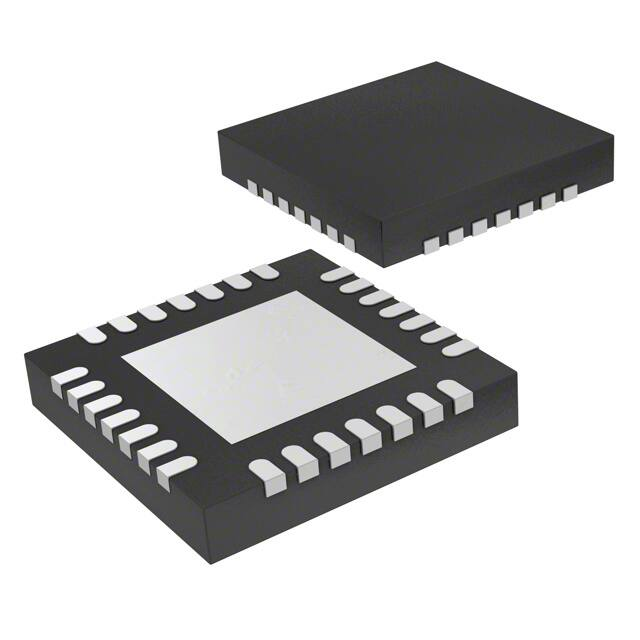
28L 4×4 WQFN
APPLICATIONS
•
Notebook/Netbook LCD Display Backlighting
DESCRIPTION
The TPS61195 IC provides highly integrated solutions for large-size LCD backlighting. This device has a built-in
high efficiency boost regulator with integrated 2.5A/50V power MOSFET. The eight current sink regulators
provide high precision current regulation and matching. In total, the device can support up to 96 LEDs. Unused
sinks are disabled by tying them to ground. The boost output automatically adjusts its voltage to the WLED
forward voltage to improve efficiency.
The TPS61195 supports multiple brightness dimming methods. During PWM dimming, each IFB pin’s current is
turned on/off at the duty cycle and frequency determined by an integrated pulse width modulation (PWM). The
frequency of this signal is resistor programmable, while the duty cycle is controlled directly either from an
external PWM signal input to the DPWM pin or through the SMBUS interface. Additionally, the SMBUS interface
provides some operational reporting data such as if one or more strings have failed or if the IC is over-heating. In
direct PWM dimming mode, each IFB current is turned on/off at same duty cycle and frequency as the PWM
signal input on the DPWM pin. In analog dimming mode, the input PWM duty cycle information is translated to
analog signal to control the WLED current signal linearly over 1% to 100% brightness area.
The TPS61195 integrates over-current and short-circuit protection, soft start and over temperature protection
circuit. The device also provides programmable output over-voltage protection, and the threshold is adjusted by
external resistor divider combination.
The TPS61195 IC has built-in linear regulator for the IC supply. The device is in a 4x4 mm QFN package.
1
Please be aware that an important notice concerning availability, standard warranty, and use in critical applications of Texas
Instruments semiconductor products and disclaimers thereto appears at the end of this data sheet.
PRODUCTION DATA information is current as of publication date.
Products conform to specifications per the terms of the Texas
Instruments standard warranty. Production processing does not
necessarily include testing of all parameters.
Copyright © 2010, Texas Instruments Incorporated
�TPS61195
SLVSA07A – MAY 2010 – REVISED AUGUST 2010
www.ti.com
TPS61195 TYPICAL APPLICATION
L1
10uH
4.5V~21V
D1
C3
4.7uF
C1
4.7uF
SW1
VIN
VDDIO
C2
1 uF
SEL1 SEL2
Mode
Interface
R7
2KΩ
R8
2KΩ
R2
43.2KΩ
VDDIO GND Internal Freq. SMBus
PWM
GND VDDIO Analog
SMBus
GND Open Analog
PWM
R6
45.3K
SW2
PGND1
PGND2
EN
TPS61195
DPWM
OVP
FDPWM
FDIM
R4
953KΩ
FSW
R3
523KΩ
SEL1
SEL2
ISET
Open GND Internal Freq. PWM
GND GND Direct PWM
R5
1M
C4
1uF
R1
65KΩ
IFB1
IFB2
IFB3
IFB4
IFB5
IFB6
IFB7
IFB8
SDA
SCL
AGND
2
FDPWM
FSW
VIN
EN
SW1
SW2
OVP
PINOUT
28
27
26
25
24
23
22
DPWM
1
21 PGND1
SEL1
2
20 PGND2
SEL2
3
19 NC
VDDIO
4
SDA
5
17 ISET
SCL
6
16 NC
IFB1
7
15 IFB8
TPS61195
8
9
10
11
12
13
14
IFB2
IFB3
IFB4
AGND
IFB5
IFB6
IFB7
18 FDIM
Submit Documentation Feedback
Copyright © 2010, Texas Instruments Incorporated
Product Folder Link(s): TPS61195
�TPS61195
www.ti.com
SLVSA07A – MAY 2010 – REVISED AUGUST 2010
PIN FUNCTIONS
PIN
NO.
DESCRIPTION
NAME
1
DPWM
PWM signal input pin. The frequency of PWM signal must be in the range of 200Hz to 20kHz
2
SEL1
Dimming mode selection pin. See Table 1 for a detailed explanation.
3
SEL2
Dimming mode selection pin. See Table 1 for a detailed explanation.
4
VDDIO
Serial bus voltage level pin. This pin should only have the recommended capacitive load.
5
SDA
SMBus data input/output pin
6
SCL
SMBus clock input pin
IFB1 to IFB4
IFB5 to IFB8
Regulated 30mA typical current sink input pins. Connect the cathode of the last LED in each of the
eight strings to one of these pins.
11
AGND
Analog ground
16
N.C
AGND internal. External to AGND is recommended.
17
ISET
Full-scale LED current set pin. Connecting a resistor from this pin to AGND programs the
maximum current level.
18
FDIM
Dimming frequency program pin with an external resistor. Connecting a resistor from this pin to
AGND programs the internal PWM dimming frequency.
19
N.C
AGND internal. External track tie to AGND is recommended.
PGND2, PGND1
Power ground
OVP
Over-voltage program pin. A resistor divider between the boost converter output to AGND, with
mid point tied to this pin sets the over-voltage protection threshold.
7–10, 12–15
20, 21
22
23,24
SW2, SW1
Drain connection of the internal power FET
25
EN
SDAble and Disable Pin. EN high = SDAble, EN low = Disable and de-actives SMBus interface.
26
VIN
Supply input pin
27
FSW
Switching frequency select pin. Use a resistor to set the frequency between 600kHz to 1.0MHz
28
FDPWM
Place a 43.2kΩ resistor from this pin to AGND programming the internal clock for counting PWM
input duty cycle.
Submit Documentation Feedback
Copyright © 2010, Texas Instruments Incorporated
Product Folder Link(s): TPS61195
3
�TPS61195
SLVSA07A – MAY 2010 – REVISED AUGUST 2010
www.ti.com
FUNCTIONAL BLOCK DIAGRAM
L
Diode
V IN
SW 1
C4
1 mF
VIN
VDDIO
OVP
Slope
Compensation
C2
0.1 mF
PGND
1,2
S
Vref
Comp
Error
Amp
FSW
Oscillator
A
D
M
U
X
R3
SEL
ISET
IFB 1
Current REF
R1
PWM Signal
Generator
A
D
Duty
Control
R2
00h
01h
02h
03h
SCL
SDA
EN
BL_CTL
PWM_MD
PWM_SEL
SMBus
Interface
EN
Current Sink
R4
DPWM
FDPWM
EA
Dimming
Control
FDIM
R6
IFB1
IFB2
IFB3
IFB4
IFB5
IFB6
IFB7
IFB8
Dimming Mode
Select
Current Mirror
R5
OVP
Shutdown Boost
R Q
S
Linear
Regulator
C3
4.7 mF
SW 2
Detector
C1
4.7 mF
OUTPUT
SMBus
AGND
Current Sink
IFB 2
Current Sink
IFB 3
Current Sink
IFB 4
Current Sink
IFB 5
Current Sink
IFB 6
Current Sink
IFB 7
Current Sink
IFB 8
Shutdown
ORDERING INFORMATION
4
PACKAGE
PACKAGE MARKING
TPS61195RUY
TPS61195
Submit Documentation Feedback
Copyright © 2010, Texas Instruments Incorporated
Product Folder Link(s): TPS61195
�TPS61195
www.ti.com
SLVSA07A – MAY 2010 – REVISED AUGUST 2010
ABSOLUTE MAXIMUM RATINGS (1)
over operating free-air temperature range (unless otherwise noted)
Voltages on pin VIN
(2)
Voltages on pin EN, DPWM, SDA and SCL
(2)
VALUE
UNIT
–0.3 to 24
V
–0.3 to 7
V
Voltage on pin SW1 and SW2 (2)
–0.3 to 50
V
Voltage on pin IFB1 to IFB8 (2)
–0.3 to 20
V
Voltage on all other pins (2)
–0.3 to 3.6
V
HBM
2
kV
MM
200
V
CDM
700
V
ESD rating
Continuous power dissipation
See Dissipation Rating Table
Operating junction temperature range
–40 to 150
°C
Storage temperature range
–65 to 150
°C
260
°C
Lead temperature (soldering, 10 sec)
(1)
(2)
Stresses beyond those listed under absolute maximum ratings may cause permanent damage to the device. These are stress ratings
only, and functional operation of the device at these or any other conditions beyond those indicated under recommended operating
conditions is not implied. Exposure to absolute-maximum-rated conditions for extended periods may affect device reliability.
All voltage values are with respect to network ground terminal.
THERMAL INFORMATION
THERMAL METRIC (1)
TPS61195
RUY (28 PINS)
qJA
Junction-to-ambient thermal resistance
34.3
qJCtop
Junction-to-case (top) thermal resistance
31.3
qJB
Junction-to-board thermal resistance
9.5
yJT
Junction-to-top characterization parameter
0.2
yJB
Junction-to-board characterization parameter
8.6
qJCbot
Junction-to-case (bottom) thermal resistance
2.1
(1)
UNITS
°C/W
For more information about traditional and new thermal metrics, see the IC Package Thermal Metrics application report, SPRA953.
RECOMMENDED OPERATING CONDITIONS
MIN
TYP
MAX
UNIT
VIN
Input voltage range
4.5
21
V
VOUT
Output voltage range
Vin
45
V
L
Inductor
4.7
10
mH
CI
Input capacitor
CO
Output capacitor
2.2
FPWM_O
IFBx PWM dimming frequency set by resistor to ANGD on FDIM
0.2
FPWM_I
1
PWM input signal frequency (SMBus mode)
mF
10
mF
5
kHz
10
kHz
PWM input signal frequency (PWM mode)
0.2
20
FBOOST
Boost regulator switching frequency
600
1000
kHz
TA
Operating ambient temperature
–40
85
°C
TJ
Operating junction temperature
–40
125
°C
Submit Documentation Feedback
Copyright © 2010, Texas Instruments Incorporated
Product Folder Link(s): TPS61195
5
�TPS61195
SLVSA07A – MAY 2010 – REVISED AUGUST 2010
www.ti.com
ELECTRICAL CHARACTERISTICS
VIN = 12V, DPWM and EN = high, IFB current = 20mA, IFB voltage = 500mV, TA = –40°C to 85°C, typical values are at TA =
25°C (unless otherwise noted)
PARAMETER
TEST CONDITIONS
MIN
TYP
MAX
UNIT
SUPPLY CURRENT
VIN
Input voltage range
4.5
Iq_VIN
Operating quiescent current into VIN
Not Switching and no load,
VIN = 21V
VDDIO
VDDIO pin output voltage
VIN > 5.5V, Iload = 5 mA
IEN
Shutdown current
VIN = 12V, EN = low
VIN = 21V, EN = low
VIN_UVLO
VIN under-voltage lockout threshold
VIN ramp down
VIN ramp up
VIN_Hys
VIN under-voltage lockout hysterisis
2.7
3.15
21
V
3
mA
3.6
V
10
15
mA
3.55
3.80
V
250
mV
EN, SCL, SDA AND PWM
VH
EN Logic high threshold
1.2
V
VL
EN Logic low threshold
VH
DPWM logic high threshold
VL
DPWM logic low threshold
VH
SDA, SCL logical high threshold
VL
SDA, SCL logic low threshold
VSDA_L
SDA logic low voltage
RPD_EN
Pull down resistor on EN
400
800
1600
kΩ
RPD_PWM
Pull down resistor on DPWM
400
800
1600
kΩ
12.5
100
mA
nA
MΩ
0.4
2.1
0.7
V
2.0
0.8
ISOURCE = 4 mA
V = 5V
V = 0V
Ileakage
Leakage current on EN and DPWM
RPD_SMBus
Pull down resistor on SCL and SDA
0.4
3.125
–100
1
2
4
1.204
1.229
1.253
V
CURRENT REGULATION
VISET
ISET pin voltage
KISET
Current multiply IFB/ISET
IISET = 18.9 mA, D = 100%
IFB_AVG
Average current accuracy
IISET = 18.9 mA, D = 100%
TA= 0°C to 85°C
IFB_L
Low current accuracy
IISET = 18.9 mA, D = 12.5%, analog
TA= 0°C to 85°C
Km
(Imax–Imin)/IAVG
IISET = 18.9 mA, D = 100%
TA= 0°C to 85°C
Ileak
IFB pin leakage current
IFB voltage = 15 V on all pins
IFB voltage = 5 V on all pins, total
IIFB_max
Current sink max output current
IFB = 450 mV
IIFB_range
Programmable current sink regulator
range
fdim
Internal PWM dimming frequency
–1.5%
+1.5%
–5%
+5%
1%
3%
5
1
30
190
mA
mA
0
RFDIM = 953kΩ
V
1060
210
30
mA
230
Hz
BOOST OUTPUT REGULATION
VIFB_L
Output voltage dial up threshold
Measured on VIFB(min)
450
mV
VIFB_H
Output voltage dial down threshold
Measured on VIFB(min)
750
mV
0.15
POWER SWITCH
RPWM_SW
PWM FET on-resistance
VIN = 12V
ILN_NFET
PWM FET leakage current
VSW = 50V, TA = 25°C
6
Submit Documentation Feedback
0.35
Ω
2
mA
Copyright © 2010, Texas Instruments Incorporated
Product Folder Link(s): TPS61195
�TPS61195
www.ti.com
SLVSA07A – MAY 2010 – REVISED AUGUST 2010
ELECTRICAL CHARACTERISTICS (continued)
VIN = 12V, DPWM and EN = high, IFB current = 20mA, IFB voltage = 500mV, TA = –40°C to 85°C, typical values are at TA =
25°C (unless otherwise noted)
PARAMETER
TEST CONDITIONS
MIN
TYP
MAX
UNIT
0.8
1.0
1.2
MHz
OSCILLATOR
fS
Oscillator frequency
RFSW = 523kΩ
Dmax
Maximum duty cycle
IFB = 0V
Dmin
Minimum duty cycle
RFSW = 523kΩ
94%
10%
OC, SC, OVP AND SS
ILIM
N-Channel MOSFET current limit
VCLAMP_TH
Output voltage clamp program threshold
1.90
1.95
2.00
VOV_TH
Output over voltage program threshold
1.98
2.03
2.08
V
VOVP_IFB
IFB overvoltage threshold
12.5
14
15.5
V
nd
D = Dmax
2.5
Measured on the IFBx pin, IFB on
Level IFB overvoltage threshold
Measured on the IFBx pin, IFB on or off
4.5
VOVP2_IFB
2
VIFB_nouse
IFB no use detection threshold during
startup
IFB voltage rising
18
0.75
VOL
OVP pin overload detection
Output voltage drop
60%
A
V
V
THERMAL SHUTDOWN
Tshutdown
Thermal shutdown threshold
150
Submit Documentation Feedback
Copyright © 2010, Texas Instruments Incorporated
Product Folder Link(s): TPS61195
°C
7
�TPS61195
SLVSA07A – MAY 2010 – REVISED AUGUST 2010
www.ti.com
TYPICAL CHARACTERISTICS
TABLE OF GRAPHS
FIGURE
Load efficiency TPS61195
Vin = 10.8 V; Vout = 33, 37 and 41V; L = 10 mH
Figure 1
Load efficiency TPS61195
Vin =7 V, 10.8 V and 21V, Vout = 33V; L = 10 mH
Figure 2
PWM dimming efficiency
Vin = 7 V, 10.8 V and 21V, Vout = 41V; L = 10 mH; ISET = 18.9 mA
Figure 3
PWM dimming efficiency
Vin = 7 V, 10.8 V and 21V, Vout = 33V; L = 10 mH; ISET = 18.9 mA
Figure 4
Dimming linearity
Vin = 10.8 V; Vout = 41 V; L = 10 µH; ISET = 18.9 mA; FDIM = 2 kHz
Figure 5
Dimming linearity
Vin = 10.8 V; Vout = 41 V; L = 10 µH; ISET = 18.9 mA; FDIM = 210 Hz
Figure 6
Boost switch Frequency
Vin = 10.8 V; Vout = 41 V; L = 10 µH; ISET = 18.9 mA
Figure 7
Dimming Frequency
Vin = 10.8 V; Vout = 41 V; L = 10 µH; ISET = 18.9 mA
Figure 8
Switch waveform
Vin = 10.8 V; Vout = 41 V; L = 10 µH; ISET = 18.9 mA
Figure 9
Switch waveform
Vin = 21.0 V; Vout = 41 V; L = 10 µH; ISET = 18.9 mA
Figure 10
Analog dimming
Vin = 10.8 V; Vout = 41 V; L = 10 µH; ISET = 18.9 mA; FDIM = 210 Hz; D = 45%
Figure 11
Direct PWM dimming
Vin = 10.8 V; Vout = 41 V; L = 10 µH; ISET = 18.9 mA; FDIM = 210 Hz; D = 50%
Figure 12
Output ripple when PWM dimming
Vin = 10.8 V; Vout = 41 V; L = 10 µH; ISET = 18.9 mA; FDIM = 210 Hz
Figure 13
Startup waveform
Vin = 10.8 V; Vout = 41 V; L = 10 µH; ISET = 18.9 mA
Figure 14
EFFICIENCY vs LOAD
EFFICIENCY vs LOAD
100
100
VIN = 10.8 V
98
94
94
92
92
90
VOUT = 37 V
88
VOUT = 41 V
86
88
82
82
80
80
78
78
76
76
50
100
150
200
IO - Output Current - mA
250
300
VIN = 7 V
86
84
0
74
0
Figure 1.
8
VIN = 10.8 V
90
84
74
VIN = 21 V
96
VOUT = 33 V
Efficiency - %
Efficiency - %
96
VOUT = 33 V
98
VOUT = 29 V
50
100
150
200
IO - Output Current - mA
250
300
Figure 2.
Submit Documentation Feedback
Copyright © 2010, Texas Instruments Incorporated
Product Folder Link(s): TPS61195
�TPS61195
www.ti.com
SLVSA07A – MAY 2010 – REVISED AUGUST 2010
EFFICIENCY vs PWM DUTY
EFFICIENCY vs PWM DUTY
100%
100%
VOUT
VOUT = 33V
90%
90%
80%
80%
70%
70%
VIN =21V
Efficiency (%)
Efficiency (%)
VIN =10.8V
VIN=10.8V
V IN=7V
60%
50%
VIN =7V
60%
50%
40%
40%
30%
30%
20%
VIN =21V
20%
0
20
40
60
PWM - %
80
100
0
20
40
60
PWM - %
Figure 4.
Figure 3.
IO vs DIMMING DUTY CYCLE
100
IO vs DIMMING DUTY CYCLE
160
160
VIN = 10.8 V,
FDIM = 2 kHz
140
VIN = 10.8 V,
FDIM = 210 Hz
140
120
IO - Output Current - mA
120
IO - Output Current - mA
80
100
80
60
40
20
100
80
60
40
20
0
0
0
20
40
60
80
100
0
PWM Duty Cycle - %
20
40
60
80
100
PWM Duty Cycle - %
Figure 5.
Figure 6.
Submit Documentation Feedback
Copyright © 2010, Texas Instruments Incorporated
Product Folder Link(s): TPS61195
9
�TPS61195
SLVSA07A – MAY 2010 – REVISED AUGUST 2010
www.ti.com
BOOST SWITCH FREQUENCY vs R_FSW
DIMMING FREQUENCY vs FDIM
1050
5000
Brightness Dimming Frequency - Hz
Boost Switch Frequency - kHz
950
900
850
800
750
700
650
600
550
500
VIN = 10.8 V
4600
VIN = 10.8 V
1000
4200
3800
3400
3000
2600
2200
1800
1400
1000
600
600
700
800
R_FSCLT - kW
900
1000
200
40
200
360
520
680
R_FPWM - kW
Figure 7.
Figure 8.
SWITCH WAVEFORM
SWITCH WAVEFORM
VOUT
100 mV/div
AC
VOUT
100 mV/div
AC
SW
20 V/div
DC
SW
20 V/div
DC
Inductor
Current
500 mA/div
DC
Inductor
Current
500 mA/div
DC
t - Time - 1 ms/div
t - Time - 1 ms/div
Figure 9.
Figure 10.
ANALOG DIMMING
DIRECT PWM DIMMING
VOUT
200mV/Div
AC
840
1000
VOUT
200mV/Div
AC
DPWM
5V/Div
DC
DPWM
5V/Div
DC
IFB1
10V/Div
DC
IFB1
10V/Div
DC
Output
Current
100mA/Div
DC
Output
Current
100mA/Div
DC
t - Time - 2 ms/div
t-Time-2ms/div
Figure 11.
10
Figure 12.
Submit Documentation Feedback
Copyright © 2010, Texas Instruments Incorporated
Product Folder Link(s): TPS61195
�TPS61195
www.ti.com
SLVSA07A – MAY 2010 – REVISED AUGUST 2010
INTERNAL FREQUENCY PWM DIMMING
STARTUP WAVEFORM
/SD
5 V/div
DC
VOUT
200mV/Div
AC
VDDIO
5 V/div
DC
DPWM
5V/Div
DC
VOUT
10 V/div
DC
IFB1
10V/Div
DC
Inductor
Current
500 mA/div
DC
Output
Current
100mA/Div
DC
t - Time - 4 ms/div
t-Time-2ms/div
Figure 13.
Figure 14.
DETAILED DESCRIPTION
NORMAL OPERATION
The TPS61195 is a high efficiency, high output voltage white LED driver for notebook panel backlighting
applications. The advantages of white LEDs compared to CCFL backlights are higher power efficiency and lower
profile design. Due to the large number of white LEDs required to provide backlighting for medium to large
display panels, the LEDs must be arranged in parallel strings of several LEDs in series. Therefore, the backlight
driver for battery powered systems is almost always a boost regulator with multiple current sink regulators.
Having more white LEDs in series reduces the number of parallel strings and therefore improves overall current
matching. However, the efficiency of the boost regulator declines due to the need for high output voltage. Also,
there must be enough white LEDs in series to ensure the output voltage stays above the input voltage range.
However, the TPS61195 boost regulator operates in pules skip mode if the input voltage on the VIN pin is slightly
higher than total WLED forword voltage. In pulse skip mode, the main switch turns on/off for several cycles to
charge the inductor and output capacitor. The device continues to regulate the output voltage and current sinks
continue to regulate the IFB pin current.
The TPS61195 IC has integrated all of the key function blocks to power and control up to 96 white LEDs. The
device includes a 50V/2.5A boost regulator, eight 30mA current sink regulators and protection circuits for
over-current, over-voltage and short circuit failures. Multiple IFB pins can be connected together to accommodate
high current LEDs.
The TPS61195 integrates three dimming methods including traditional "no delay" PWM dimming and analog
dimming control as well as direct PWM dimming. In addition, the TPS61195 provides two control interface
methods. These are explained in further detail in the BRIGHTNESS DIMMING CONTROL section.
SUPPLY VOLTAGE
The TPS61195 IC has a built-in LDO linear regulator to supply the IC analog and logic circuit. The regulator
output is connected to the VDDIO pin. The regulator turns on when VIN is applied to the IC but does not reach
regulation until the EN pin is pulled high. A 1µF bypass capacitor on the VDDIO pin is required for the LDO to be
control loop stable. In addition, avoid connecting the VDDIO pin to any other circuit as this could introduce the
noise into the IC supply voltage.
The voltage on the VIN pin is the input of the internal LDO, and powers the IC. There is an under-voltage lockout
on the VIN pin which disables the IC when its voltage falls to 3.55V (Maximum). The IC restarts when the VIN pin
voltage recovers by 250mV.
Submit Documentation Feedback
Copyright © 2010, Texas Instruments Incorporated
Product Folder Link(s): TPS61195
11
�TPS61195
SLVSA07A – MAY 2010 – REVISED AUGUST 2010
www.ti.com
BOOST REGULATOR AND PROGRAMMABLE SWITCH FREQUENCY (FSW)
The fixed-frequency PWM boost converter uses current-mode control and has integrated loop compensation.
The internal compensation ensures stable output over the full input and output voltage range assuming the
recommended inductance and output capacitance values in the RECOMMENDED OPERATING CONDITIONS
are used. The output voltage of the boost regulator is automatically set by the IC to minimize the voltage drop
across the IFB pins. The IC regulates the lowest IFB pin to 450mV, and consistently adjusts the boost output
voltage to account for any changes in LED forward voltages. If the input voltage is higher than the sum of the
white LED forward voltage drops (e.g. at low duty cycles), the boost converter will not be able to regulate the
output due to its minimum duty cycle limitation. In this case, increase the number of WLED in series or include
series ballast resistors in order to provide enough headroom for the converter to boost the output voltage. Since
the TPS61195 integrates a 2.5A/50V power MOSFET, the boost converter can provide up to a 45V output
voltage.
The TPS61195 switch frequency is programmable between 600 KHz to 1.0 MHz by the resistor value on the
FSW pin and roughly following Equation 1:
FSW »
5.23 ´ 1011
RFSW
(1)
Where
RFSW = FSW pin resistor
See Figure 7 for boost converter switching frequency adjustment resistor RFSW selection.
The adjustable switching frequency feature provides the user with the flexibility of choosing a faster switching
frequency, and therefore, an inductor with smaller inductance and footprint or slower switching frequency, and
therefore, potentially higher efficiency due to lower switching losses.
LED CURRENT SINKS
The eight current sink regulators embedded in TPS61195 can be collectively configured to provide up to a
maximum of 30mA. These eight specialized current sinks are accurate to within -3% minimum and +2%
maximum for currents above 10 mA, with a string-to-string difference of ±1% . The IFB current must be
programmed to the highest WLED current expected using the ISET pin resistor and the following Equation 2.
V
IFB = ISET ´ KISET
RISET
(2)
Where
KISET = Current multiple (1060 typical)
VISET = ISET pin voltage (1.229V typical)
RISET = ISET pin resistor
ENABLE AND SOFT STARTUP
The TPS61195 integrats power up sequency control circuit which provides free power up sequency to system. A
logic high signal on the EN pin turns on the internal LDO linear regulator which provides VDDIO to activate the
IC. After the device is disabled, the TPS61195 checks the status of all current feedback channels and shuts
down any unused feedback channels.
After the device is enabled, if the PWM pin is left floating, the output voltage of TPS61195 regulates to the
minimum output voltage. Once the IC detects a voltage on the PWM pin, the TPS61195 begins to regulate the
IFB pin current, as pre-set per the ISET pin resistor, times the duty cycle of the signal on the PWM pin. The
boost converter’s output voltage rises to the appropriate level to accommodate the sum of the white LED string
with the highest forward voltage drops plus 450mV typical at that current.
The TPS61195 has an integrated soft-start circuit to avoid any inrush current during the startup. During the
startup period, the output voltage rises from minimum output voltage in approximately 100mV increments. The
output voltage will not stop rising until all IFB pin voltages are above 450mV and all IFB pin currents are sinking
the pre-set value. The startup period depends on the expected output voltage and can be predicted
byEquation 3.
12
Submit Documentation Feedback
Copyright © 2010, Texas Instruments Incorporated
Product Folder Link(s): TPS61195
�TPS61195
www.ti.com
SLVSA07A – MAY 2010 – REVISED AUGUST 2010
æ
ö
R6
- 0.72 V ÷
t = K ´ ç VOUT ´
R5+R6
è
ø
(3)
Where
K= 26ms/V
Pulling the EN pin low immediately shuts down the IC, resulting in the IC consuming less than 50µA in the
shutdown mode.
UNUSED IFB PIN
If the application requires less than 8 WLED strings, one can easily disable unused IFB pins. The TPS61195
simply requires leaving the unused IFB pin open or shorting it to ground. If the IFB pin is open, the boost output
voltage ramps up to the preset over-voltage threshold set per the VOVP pin during start up. The IC then detects
the zero current string, and removes it from the feedback loop. If the IFB pin is shorted to ground, the IC detects
the voltage less than VIFB_nouse threshold typically 0.75V and immediately disables the string after the IC is
enabled. Thus, the boost output voltage ramps to the regulation voltage immediately following soft start and does
not go up to the over-voltage threshold.
BRIGHTNESS DIMMING CONTROL
The TPS61195 integrates several methods of dimming control and two user control interfaces as summarized in
the TYPICAL APPLICATION CIRCUIT and Table 1. If the PWM interface is selected then all of the methods are
a function of the input PWM signal duty cycle. If the SMBus interface is selected, then the white LED brightness
is adjustable through a standard SMBus 2.0 instruction set which is fully compatible with the DELL white LED
backlighting SMBus protocol. An added benefit of using the SMBus interface is digital reporting of operation
conditions.
The no-delay PWM dimming method uses the internal PWM dimming frequency, set by the resistor on the FDIM
pin, while direct PWM dimming uses the frequency supplied by the input signal on the DPWM pin. Compared to
analog dimming, PWM dimming provides better brightness linearity and less color shift over the entire PWM
dimming range. With direct and no-delay PWM dimming implemented, the IC turns on and off all eight current
sink regulators at the same duty cycle as the input PWM signal. See section NO DELAY PWM DIMMING.
The IC also can also be configured for analog dimming. In this mode, the IC modulates all eight current sink
regulators as a function of the input PWM signal duty cycle. Compared to PWM dimming, analog dimming
provides higher power and electrical to optical efficiency as well as eliminates output ripple that can cause some
ceramic output capacitors to generate audible noise.
Table 1. Brightness Control and Dimming Method List
SEL1
SEL2
MODE
INTERFACE
VDDIO
GND
No delay PWM
SMBus
OPEN
GND
No delay PWM
PWM
GND
VDDIO
Analog
SMBus
GND
OPEN
Analog
PWM
GND
GND
Direct PWM
PWM
ADJUSTABLE PWM DIMMING FREQUENCY (FDIM)
The TPS61195 has a built-in oscillator to generate the internal PWM dimming signal. Each IFB current regulator
sink is turned on/ off at this oscillator's frequency. The built-in oscillator's frequency is adjustable with an external
resistor RFDIM on the FDIM pin in the range of 100Hz to 5KHz roughly following Equation 4:
FDIM »
2 ´ 108
RFDIM
(4)
Where
RFDIM = FDIM pin resistor
Submit Documentation Feedback
Copyright © 2010, Texas Instruments Incorporated
Product Folder Link(s): TPS61195
13
�TPS61195
SLVSA07A – MAY 2010 – REVISED AUGUST 2010
www.ti.com
The adjustable range of the RFDIM resistor is from 40kΩ to 1MΩ, corresponding to the dimming frequency, FDIM,
of 200Hz to 5kHz. See Figure 8 for PWM dimming frequency adjustment resistor RFDIM selection and Table 2 for
the resistor value recommendation list.
Table 2. RFDIM Recommendations
RFDIM
FDIM
953 kΩ
210 Hz
200 kΩ
1 kHz
100 kΩ
2 kHz
PWM AND SMBUS INPUT BRIGHTNESS CONTROL INTERFACE
The TPS61195 controls the white LED brightness by the PWM signal on the PWM pin or SMBus instruction input
on the SCL and SDA pins. Using the PWM control interface, the TPS61195 integrates a high-speed,
high-precision digital counter to calculate the PWM duty cycle on the PWM pin. The PWM duty cycle digital
counter auto-adjusts the sample rate for a 200Hz to 20 kHz PWM input signal. The key benefit of the digital
counter is cycle-by-cycle high-speed sampling and computing which allows the current sinks to easily respond to
the input PWM duty cycle within one cycle. After counting, the input PWM duty cycle information is saved as in
an eight-bit internal register. Alternatively, under SMBus control, the user sends the eight-bit brightness
information to the TPS61195 for direct storage in the internal register. The TPS61195 turns on and off each IFB
current channel using the duty cycle information that is stored in this internal register.
A 43.2kΩ resistor is required on the FDPWM pin to set the bias current for the internal digital counter.
NO DELAY PWM DIMMING
In this mode, all used IFB channels are turn on and off together at the FDIM frequency which is set by RFDIM on
the FDIM pin. Figure 15 gives the timing diagram for each channel in No Delay PWM dimming mode.
D = 35%
TON
PWM
TPWM
TDIM
ILED
D = 35%
IFB1
IFB2
IFB3
IFB8
Figure 15. No Delay PWM Dimming Timing Diagram
14
Submit Documentation Feedback
Copyright © 2010, Texas Instruments Incorporated
Product Folder Link(s): TPS61195
�TPS61195
www.ti.com
SLVSA07A – MAY 2010 – REVISED AUGUST 2010
Table 3 gives the recommended dimming duty cycle range for various input PWM signal frequencies when using
No Delay PWM Dimming mode.
Table 3. Recommended Dimming Duty Cycle Range
per PWM Frequency when using No Delay PWM
Dimming
PWM Input Signal
Frequency (Hz)
Dmin(%)
Dmax(%)
100< f ≤ 200
1
100
200< f ≤ 500
1
100
500< f ≤ k
1
100
1k< f ≤ 2k
1
100
2k< f ≤ 5k
1
100
5k< f ≤ 10k
4
100
DIRECT PWM DIMMING
In direct PWM dimming mode, all used IFB channels turn on and off together at the same frequency and duty
cycle as the input PWM on the PWM pin. Figure 16 is the timing diagram for direct PWM dimming.
D = 50%
PWM
D = 35%
D = 10%
TON
TPWM
ILED
IFB1
IFB2
IFB3
IFB8
Figure 16. Direct PWM Dimming Timing Diagram
Table 4 gives the recommended input dimming duty cycle range for various input PWM signal frequencies when
using Direct PWM Dimming mode.
Table 4. Recommended Dimming Duty Cycle Range
per PWM Frequency when using Direct PWM Dimming
PWM Input Signal
Frequency (Hz)
Dmin(%)
Dmax(%)
100< f ≤ 200
0.5
100
200< f ≤ 500
1
100
500< f ≤ 1k
1
100
Submit Documentation Feedback
Copyright © 2010, Texas Instruments Incorporated
Product Folder Link(s): TPS61195
15
�TPS61195
SLVSA07A – MAY 2010 – REVISED AUGUST 2010
www.ti.com
Table 4. Recommended Dimming Duty Cycle Range
per PWM Frequency when using Direct PWM
Dimming (continued)
PWM Input Signal
Frequency (Hz)
Dmin(%)
Dmax(%)
1k< f ≤ 2k
2
100
2k< f ≤ 5k
5
100
5k< f ≤ 10k
10
100
10k< f ≤ 20k
20
100
ANALOG DIMMING
In analog dimming mode, all used current sinks are always on, with each current sink being linearly controlled
from 0% to 100% of the maximum IFB current by the duty cycle brightness information stored in the brightness
register. Figure 17 shows a simple current diagram of analog dimming mode with PWM brightness control.
D = 50%
PWM
D = 35%
D = 12.5%
D = 6.25%
TON
TPWM
ILED
IFB1
0
IFB2
IFB3
IFB8
Figure 17. Analog Dimming Timing Diagram
OUTPUT VOLTAGE CLAMP AND OVER VOLTAGE PROTECTION
The TPS61195 has two levels of protection against the output, and therefore the SW pins, exceeding a certain
voltage. The output voltage clamp circuit limits the output voltage to the user selected value by limiting the
internal feedback loop reference level. The clamp circuit's response time is not fast enough to protect against
output voltage transients or high-voltage noise spikes that couple from external circuits. So, if the over-voltage
(OV) circuit detects the output going 80mV higher than the clamp voltage, it turns off the boost switch until the
output voltage drops below the clamp voltage. Resistors R5 and R6 in the TYPICAL APPLICATION set the
output voltage clamp threshold and OV threshold as computed by Equation 5 and Equation 6.
æ R5 ö
VOUT_CLAMP = VCLAMP_TH ´ ç 1+
÷
è R6 ø
(5)
æ R5 ö
VOUT_OV = VOV_TH ´ ç 1+
÷
è R6 ø
(6)
In the TYPICAL APPLICATION, the output OVP voltage is set to:
1M ö
æ
VOUT_CLAMP = 1.95 ´ ç 1+
÷ = 45 V
è 45.3K ø
16
Submit Documentation Feedback
(7)
Copyright © 2010, Texas Instruments Incorporated
Product Folder Link(s): TPS61195
�TPS61195
www.ti.com
SLVSA07A – MAY 2010 – REVISED AUGUST 2010
1M ö
æ
VOUT_OV = 2.03 ´ ç 1+
÷ = 46.8 V
45.3K
è
ø
(8)
CURRENT SINK OPEN PROTECTION
For the TPS61195, if one of the WLED strings is open, the boost output rises to over-voltage threshold. The IC
detects the open WLED string by sensing no current in the corresponding IFB pin. As a result, the IC deactivates
the open IFB pin and removes it from the voltage feedback loop. Subsequently, the output voltage drops and is
regulated to the minimum voltage required for the connected WLED strings. The IFB current of the connected
WLED string remains in regulation during this process.
If any IFB pin voltage exceeds the IFB over-voltage threshold (14V typical), the IC turns off the corresponding
current sink and removes this IFB pin from output voltage regulation loop. The remaining IFB pins’ current
regulation is not affected. This condition often occurs when there are several shorted WLEDs in one string.
WLED mismatch typically does not create such large voltage difference among WLED strings.
If the open string is reconnected again, Power-on reset (POR), EN pin toggling or SMBus instruction is required
to reactivate a previously deactivated string. The IC will continuously auto-restart if it detects that all of the WLED
strings are open until at least one string closes the loop between the boost converter output and one IFB pin.
OVER CURRENT AND SHORT CIRCUIT PROTECTION
The TPS61195 has pulse-by-pulse over-current limit of 2.5A (min). The PWM switch turns off when the inductor
current reaches this current threshold. The PWM switch remains off until the beginning of the next switching
cycle. This protects the IC and external components under over-load conditions. When there is a sustained
over-current condition, the IC turns off and requires POR or the EN pin toggling to restart.
Under severe over-load and/or short circuit conditions, the boost output voltage can be pulled below the required
regulated voltage to keep all of the white LEDs operating. Under this condition, the current flows directly from
input to output through the inductor and schottky diode. To protect the TPS61195, the device shuts down
immediately. The IC restarts after input POR or EN pin logic toggling or SMBus instruction.
THERMAL PROTECTION
When the junction temperature of the TPS61195 is over 150°C (typ), the thermal protection circuit is triggered
and shuts down the device immediately. The device automatically restarts when the junction temperature is back
to less than 150°C with about 15°C hysteresis.
SMBUS INTERFACE CONTROL
TPS61195 can be controlled by the SMBus if selected by the mode pin SEL1. The TPS61195 includes four
registers to control and monitor the brightness, fault status, operating mode and identification. The slave address
of the device has 7 fixed bits and 1 read or write bit as Figure 18 shows. If the device is requested to read, the
R/W bit is set to1, otherwise the R/W bit is set to 0.
MSB
LSB
1
0
1
0
0
R/W
Device Address
R
ea
d/
W
Device Identifier
1
rit
e
0
Figure 18. TPS61195 Slave Address
READ BYTE
As shown in Figure 19, the four byte long Read Byte protocol starts with the slave address followed by the
"command code" which translates to the "register index". Then the bus direction turns around with the
re-broadcast of the slave address with bit 0 indicating a read cycle. The fourth byte contains the data being
returned by the backlight controller. That byte value in the data byte should reflect the value of the register being
queried at the "command code" index. A dark grey outline is used on cycles during which the backlight controller
"owns" or "drives" the Data line. All other cycles are driven by the "host".
Submit Documentation Feedback
Copyright © 2010, Texas Instruments Incorporated
Product Folder Link(s): TPS61195
17
�TPS61195
SLVSA07A – MAY 2010 – REVISED AUGUST 2010
Write
Start Condition
S
0
1
www.ti.com
0
1
1
0
0
0
A
Read
Bit7 Bit6 Bit5 Bit4 Bit3 Bit2 Bit1 Bit0
TPS61195 Address
A
Register Index
0
1
0
1
1
0
0
1
A
Bit7 Bit6 Bit5 Bit4 Bit3 Bit2 Bit1 Bit0
TPS61195 Address
A
P
Register Data
Slave to Master
Master to Slave
Figure 19. TPS61195 SMBus Read Byte Protocol
WRITE BYTE
The Write Byte protocol is only three bytes long. The first byte starts with the slave address again followed by the
"command code" which translates to the "register index" being written. The third byte contains the data byte that
must be written into the register selected by the "command code". Again note the bus directions as highlighted
by the dark grey outline.
Write
Start Condition
S
0
1
0
1
1
0
0
0
A
Bit7 Bit6 Bit5 Bit4 Bit3 Bit2 Bit1 Bit0
TPS61195 Address
A
Bit7 Bit6 Bit5 Bit4 Bit3 Bit2 Bit1 Bit0
A
P
Register Data
Register Index
Slave to Master
Master to Slave
Figure 20. TPS61195 SMBus Write Byte Protocol
SMBUS REGISTER DESCRIPTION
All backlight controller registers are one byte wide and accessible via the Read/Write Byte protocols. Their bit
assignments are provided in the following sections with reserved bits containing a default value of "0".
Brightness Control Register (0x00)
This register is both readable and writable with one byte length, BRT0~BRT7 which could be used to control the
white LED brightness level in 255 steps. In SMBus control mode, a SMBus write cycle to register 0x00 sets the
brightness level. Setting this register to 0xFF implements the maximum brightness output, while setting the value
to 0x00 sets the brightness output to 0% of maximum brightness. The default value of this register is 0xFF. The
register returns the current brightness level in the register read cycle.
REGISTER 0x00
BRIGHTNESS CONTROL REGISTER
BRT7
Bit 7 (R/W)
BRT6
Bit 6 (R/W)
BRT5
Bit 5 (R/W)
BRT4
Bit 4 (R/W)
BRT3
Bit 3 (R/W)
DEFAULT 0xFF
BRT2
Bit 2 (R/W)
BRT1
Bit 1 (R/W)
BRT0
Bit 0 (R/W)
Bit field definitions:
BRT[7..0]
256 steps of brightness level
Backlighting Control Register (0x01)
This register has two bits, PWM_MD and PWM_SEL that control the operating mode of the backlight controller,
and a single bit that controls the BL ON/OFF state. The remaining bits are reserved for future use. The register is
both readable and writable. In a read cycle, Bit 0, 1 and 2 return the operating mode code and Bit 3 to 7 return
zero. Writing a value to Bit 1 and 2 sets the operating mode while a write value 1 or 0 to Bit 0 will turn ON and
OFF the current sinks respectively.
18
Submit Documentation Feedback
Copyright © 2010, Texas Instruments Incorporated
Product Folder Link(s): TPS61195
�TPS61195
www.ti.com
SLVSA07A – MAY 2010 – REVISED AUGUST 2010
REGISTER 0x01
BACKLIGHTING CONTROL REGISTER
Reserved
Bit 7
Reserved
Bit
Reserved
Bit 5
Reserved
Bit 4
Reserved
Bit 3
DEFAULT VALUE 0x00
PWM_MD
Bit 2 (R/W)
PWM_SEL
Bit 1 (R/W)
BL_CTL
Bit 0 (R/W)
Bit field definitions:
PWM_MD
PWM_SEL
BL_CTL
PWM mode select (1 = absolute brightness, 0 = % change) default = 0
Brightness MUX select (1 = PWM pin, 0 = SMBus value) default = 0
BL On/Off (1 = On, 0 = Off) default = 0
Operating mode selected by backlighting control register bit 1 and bit 2:
PWM_MD
X
1
b
PWM_SEL
1
0
0
MODE
PWM mode
SMBus mode
DPST mode
DESCRIPTION
The brightness is determined by PWM input duty cycle only
The brightness is set by SMBus command only
The brightness is the product of SMBus command and PWM input duty cycle
Fault/status Register (0x02)
This register has six status bits that allow monitoring of the backlight controller’s operating state. Bit 0 is a logical
"OR" of all fault codes to simplify error detection. Bit 3 is a simple BL status indicator. Bit 6 and bit 7 are reserved
for future use. All reserved bits return zero when read and ignore the bit value when written. All of the bits in this
register are read-only.
REGISTER 0x02
FAULT STATUS REGISTER
RESERVED
Bit 7
RESERVED
Bit 6
2_CH_EN
Bit 5 (R)
1_CH_EN
Bit 4 (R)
BL_STAT
Bit 3 (R)
DEFAULT VALUE 0x00
OV_CURR
Bit 2 (R)
THRM_SHDN
Bit 1 (R)
FAULT
Bit 0 (R)
Bit field definitions:
2_CH_EN
1_CH_EN
BL_STAT
OV_CURR
THRM_SHDN
FAULT
The number of faulted strings is reported in bits 5 and 4.
(00 = No faults, 01 = One string fault, 11 = Two or more strings faulted)
BL status (1 = BL On, 0 = BL Off)
Input over-current (1 = Over-current condition, 0 = Current OK)
Thermal Shutdown (1 = Thermal fault, 0 = Thermal OK)
Any fault except LED open and short occurs (Logic “OR” of all the fault conditions)
Submit Documentation Feedback
Copyright © 2010, Texas Instruments Incorporated
Product Folder Link(s): TPS61195
19
�TPS61195
SLVSA07A – MAY 2010 – REVISED AUGUST 2010
www.ti.com
Identification Register (0x03)
The ID register contains two bit fields to denote the manufacturer and the silicon revision of the device. The bit
field widths were chosen to allow up to 32 vendors with up to eight silicon revisions each. This register is
read-only.
REGISTER 0x03
IDENTIFICATION REGISTER
LED PANEL
Bit 7=1
MFG3
Bit 6 (R)
MFG2
Bit 5 (R)
MFG1
Bit 4 (R)
MFG0
Bit 3 (R)
DEFAULT VALUE 0xA0
REV2
Bit 2 (R)
REV1
Bit 1 (R)
REV0
Bit 0 (R)
Bit field definitions:
LED PANEL
MFG[3..0]
REV[2..0]
Display panel use white LED backlighting = 1
Manufacturer ID (16 Vendor IDs to be specified by Dell) See Table 5
Silicon rev (Revs 0-7 allowed for silicon spins)
Table 5. Vendor IDs List
20
ID
Vendor
0
Maxim
1
Micro Semi
2
MPS
3
O2 Micro
4
TI
5
ST
6
Analog Devices
7
Taos
8
Toko
9
Rohm
10
Oki
11
Allegro
12
Semtech
13
Intersil
14
Reserved
15
Vendor ID register not implemented
Submit Documentation Feedback
Copyright © 2010, Texas Instruments Incorporated
Product Folder Link(s): TPS61195
�TPS61195
www.ti.com
SLVSA07A – MAY 2010 – REVISED AUGUST 2010
APPLICATION INFORMATION
INDUCTOR SELECTION
Because the selection of the inductor affects power supply’s steady state operation, transient behavior and loop
stability, the inductor is the most important component in switching power regulator design. There are three
specifications most important to the performance of the inductor, inductor value, DC resistance and saturation
current. The TPS61195 is designed to work with inductor values between 4.7µH and 10µH. A 4.7µH inductor are
typically available in a smaller or lower profile package, while a 10µH inductor may produce higher efficiency due
to slower switching frequency and/or lower inductor ripple. If the boost output current is limited by the
over-current protection of the IC, using a 10µH inductor and highest switching frequency maximizes the
controller’s output current capability.
The internal loop compensation for the PWM control is optimized for the external component values including
typical tolerances (refer to RECOMMENDED OPERATING CONDITIONS). RECOMMENDED OPERATING
CONDITIONSInductor values can have ±20% tolerance with no current bias. When the inductor current
approaches saturation level, its inductance can decrease 20% to 35% from the 0A value depending on how the
inductor vendor defines saturation.
In a boost regulator, the inductor DC current can be calculated as:
V
´ Iout
Idc = out
Vin ´ h
(9)
Where
Vout = boost output voltage
Iout = boost output current
Vin = boost input voltage
h = power conversion efficiency, use 90% for TPS61195 applications
The inductor current peak to peak ripple can be calculated as:
1
Ipp =
æ
1
1 ö
L ´ ç
+
÷ ´ Fs
Vin ø
è Vout - Vin
(10)
Where
Ipp = inductor peak to peak ripple
L = inductor value
Fs = switching frequency
Vout = boost output voltage voltage
Vin = boost input
Therefore, the peak current seen by the inductor is:
Ipp
Ip = Idc +
2
(11)
Select the inductor with saturation current at least 30% higher than the calculated peak current to account for the
load transient steps that occur during startup and dimming. To calculate the worse case inductor peak current,
use minimum input voltage, maximum output voltage and maximum load current.
Regulator efficiency is dependent on the resistance of its high current path and switching losses associated with
the PWM switch and power diode. Although the TPS61195 IC has optimized the internal switch resistance, the
overall efficiency is affected by the inductor’s DC resistance (DCR); Lower DCR improves efficiency. However,
there is a trade off between DCR and inductor footprint, furthermore, shielded inductors typically have higher
DCR than unshielded ones. Table 6 lists recommended inductor models.
Submit Documentation Feedback
Copyright © 2010, Texas Instruments Incorporated
Product Folder Link(s): TPS61195
21
�TPS61195
SLVSA07A – MAY 2010 – REVISED AUGUST 2010
www.ti.com
Table 6. Recommended Inductor for TPS61195
L (mH)
DCR (mΩ)
Isat (A)
Size (L×W×H mm)
A915AY-4R7M
4.7
38
1.87
5.2 × 5.2 × 3.0
A915AY-100M
10
75
1.24
5.2 × 5.2 × 3.0
SLF6028T-4R7N1R6
4.7
28.4
1.6
6.0 × 6.0 × 2.8
SLF6028T-100M1R3
10
53.2
1.3
6.0 × 6.0 × 2.8
TOKO
TDK
OUTPUT CAPACITOR SELECTION
The output capacitor is mainly selected to meet the requirement for the output ripple and loop stability. This ripple
voltage is related to the capacitor’s capacitance and its equivalent series resistance (ESR). Assuming a capacitor
with zero ESR, the minimum capacitance needed for a given ripple can be calculated by:
Cout =
(Vout
- Vin ) ´ Iout
Vout ´ Fboost ´ Vripple
(12)
Where,
Vripple = peak to peak output ripple. The additional part of ripple caused by the ESR is calculated using:
Vripple_ESR = Iout × RESR
Due to its low ESR, Vripple_ESR may be neglected for ceramic capacitor, but must be considered if tantalum or
electrolytic capacitors are used.
The controller’s output voltage also ripples due to the load transient that occurs during PWM dimming. The
TPS61195 adopts a patented technology to limit this type of output ripple even with the minimum recommended
output capacitance. In a typical application, the output ripple is less than 250mV during PWM dimming with 4.7mF
output capacitor. However, the output ripple decreases with higher output capacitances. An output capacitance
value in the range of 4.7mF to 10mF is required for loop stability.
LAYOUT CONSIDERATION
As for all switching power supplies, especially those providing high current and using high switching frequencies,
layout is an important design step. If layout is not carefully done, the regulator could show instability as well as
EMI problems. Therefore, use wide and short traces for high current paths. The input capacitor, C4 in the
TYPICAL APPLICATION, needs not only to be close to the VIN pin, but also to the GND pin in order to reduce
the input ripple seen by the IC. The input capacitor, C1 in the typical application circuit, should also be placed
close to the inductor. C2 is the filter and noise decoupling capacitor for internal linear regulator powering the
internal digital circuits. It should be placed as close as possible between the VDDIO and AGND pins to prevent
any noise insert to digital circuits. The SW pin carries high current with fast rising and falling edges. Therefore,
the connection between the pin to the inductor and Schottky should be kept as short and wide as possible. It is
also beneficial to have the ground of the output capacitor C3 close to the PGND pin since there is large ground
return current flowing through it. When laying out signal ground, it is recommended to use short traces separated
from power ground traces, and connect them together at a single point, for example on the thermal pad.
R1 in the Typical Application Circuit is current setting resistor connect to the ISET pin. To avoid unexpected
noise coupling into the ISET pin and affecting the IFB current stability, R1 needs to be close to the ISET pin and
AGND pins with short and wide trace.
Thermal pad needs to be soldered on to the PCB and connected to the GND pins of the IC. Additional thermal
vias can significantly improve power dissipation of the IC. Specially, at low input voltage and high power output
conditions, the large PCB area and more layers PCB design for thermal dissipation must be considered.
22
Submit Documentation Feedback
Copyright © 2010, Texas Instruments Incorporated
Product Folder Link(s): TPS61195
�TPS61195
www.ti.com
SLVSA07A – MAY 2010 – REVISED AUGUST 2010
TYPICAL APPLICATION CIRCUITS
L1
10uH
4.5V~21V
D1
C3
4.7uF
C1
4.7uF
R5
1M
C4
1uF
VIN
SW1
VDDIO
C2
1 uF
R7
2KΩ
EN
R8
2KΩ
DPWM
OVP
TPS61195
FDIM
FDPWM
R2
43.2KΩ
R6
45.3K
SW2
PGND1
PGND2
R4
953KΩ
FSW
R3
523KΩ
SEL1
SEL2
ISET
IFB1
IFB2
IFB3
IFB4
IFB5
IFB6
IFB7
IFB8
R1
65KΩ
SDA
SCL
AGND
Figure 21. Typical Application Circuit With PWM Control Direct PWM Dimming Configuration
L1
10uH
4.5V~21V
D1
C3
4.7uF
C1
4.7uF
R5
1M
C4
1uF
SW1
VIN
VDDIO
PGND1
PGND2
C2
1 uF
R7
2KΩ
EN
R8
2KΩ
DPWM
FDPWM
R2
43.2KΩ
TPS61195
FDIM
R4
953KΩ
R3
523KΩ
VDDIO
SEL1
SEL2
IFB1
IFB2
IFB3
IFB4
IFB5
IFB6
IFB7
IFB8
ISET
R9
10K
R10
10K
OVP
FSW
3.3V
R1
65KΩ
SDA
SCL
R6
45.3K
SW2
AGND
SMBus
Control
Figure 22. Typical Application Circuit for SMBus Control interface with Internal Frequency PWM
Dimming Setting
Submit Documentation Feedback
Copyright © 2010, Texas Instruments Incorporated
Product Folder Link(s): TPS61195
23
�TPS61195
SLVSA07A – MAY 2010 – REVISED AUGUST 2010
www.ti.com
L1
10uH
4.5V~21V
D1
C3
4.7uF
C1
4.7uF
R5
1M
C4
1uF
VIN
SW2
PGND1
PGND2
VDDIO
C2
1 uF
R7
2KΩ
EN
R8
2KΩ
DPWM
TPS611 95
R4
953KΩ
FSW
R3
523KΩ
VDDIO
SEL1
SEL2
ISET
3.3V
R9
10K
IFB1
IFB2
IFB3
IFB4
IFB5
IFB6
IFB7
IFB8
R1
65KΩ
R10
10K
OVP
FDIM
FDPWM
R2
43.2KΩ
R6
45.3K
SW1
SDA
SCL
AGND
SMBus
Control
Figure 23. Typical Application Circuit for SMBus Control interface and 6 Strings LED
L1
10uH
4.5V~21V
D1
C3
4.7uF
C1
4.7uF
R5
1M
C4
1uF
VIN
SW1
VDDIO
PGND1
PGND2
C2
1 uF
R7
2KΩ
EN
R8
2KΩ
DPWM
TPS61195
OVP
FDIM
FDPWM
R2
43.2KΩ
R4
953KΩ
FSW
R3
523KΩ
SEL1
SEL2
ISET
IFB1
IFB2
IFB3
IFB4
IFB5
IFB6
IFB7
IFB8
R1
65KΩ
SDA
SCL
R6
45.3K
SW2
AGND
Figure 24. Typical Application Circuit for 4 Strings 40mA LED
24
Submit Documentation Feedback
Copyright © 2010, Texas Instruments Incorporated
Product Folder Link(s): TPS61195
�PACKAGE OPTION ADDENDUM
www.ti.com
10-Dec-2020
PACKAGING INFORMATION
Orderable Device
Status
(1)
Package Type Package Pins Package
Drawing
Qty
Eco Plan
(2)
Lead finish/
Ball material
MSL Peak Temp
Op Temp (°C)
Device Marking
(3)
(4/5)
(6)
TPS61195RUYR
ACTIVE
WQFN
RUY
28
3000
RoHS & Green
NIPDAU
Level-2-260C-1 YEAR
-40 to 85
TPS
61195
TPS61195RUYT
ACTIVE
WQFN
RUY
28
250
RoHS & Green
NIPDAU
Level-2-260C-1 YEAR
-40 to 85
TPS
61195
(1)
The marketing status values are defined as follows:
ACTIVE: Product device recommended for new designs.
LIFEBUY: TI has announced that the device will be discontinued, and a lifetime-buy period is in effect.
NRND: Not recommended for new designs. Device is in production to support existing customers, but TI does not recommend using this part in a new design.
PREVIEW: Device has been announced but is not in production. Samples may or may not be available.
OBSOLETE: TI has discontinued the production of the device.
(2)
RoHS: TI defines "RoHS" to mean semiconductor products that are compliant with the current EU RoHS requirements for all 10 RoHS substances, including the requirement that RoHS substance
do not exceed 0.1% by weight in homogeneous materials. Where designed to be soldered at high temperatures, "RoHS" products are suitable for use in specified lead-free processes. TI may
reference these types of products as "Pb-Free".
RoHS Exempt: TI defines "RoHS Exempt" to mean products that contain lead but are compliant with EU RoHS pursuant to a specific EU RoHS exemption.
Green: TI defines "Green" to mean the content of Chlorine (Cl) and Bromine (Br) based flame retardants meet JS709B low halogen requirements of


 工商网监
湘ICP备2023018690号
工商网监
湘ICP备2023018690号
