Order
Now
Product
Folder
Support &
Community
Tools &
Software
Technical
Documents
TPS61372
SLVSEE7A – JUNE 2018 – REVISED DECEMBER 2018
TPS61372 16-V, 3.8-A Synchronous Boost With Load Disconnect
1 Features
3 Description
•
•
•
The TPS61372 is a full-integrated synchronous boost
converter with the load disconnect built-in. The device
supports output voltage up to 16 V with a 3.8-A
current limit. The input voltage ranges from 2.5-V to
5.5-V supporting applications powered by a singlecell Lithium-ion battery or 5-V bus.
1
•
•
•
•
•
•
•
•
•
•
•
•
•
Input Voltage Range: 2.5 V to 5.5 V
Output Voltage Range: up to 16 V
On-Resistance:
– Low-Side FET - 33 mΩ
– High-Side FET - 104 mΩ
Switch Peak Current Limit: 3.8 A
Quiescent Current From VIN: 74 μA
Quiescent Current From VOUT: 10 μA
Shutdown Current From VIN: 1 μA
Switching Frequency: 1.5 MHz
Soft-start time: 0.9 ms
Hiccup Output Short Protection
Auto PFM and Forced PWM Selectable
Load Disconnect During Shutdown
External Loop Compensation
Output Overvoltage Protection
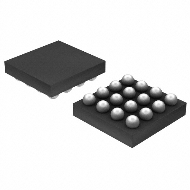
1.57-mm × 1.52-mm × 0.5 mm 16-Pin WCSPs
Create a Custom Design Using the TPS61372
With WEBENCH® Power Designer
The TPS61372 uses the peak current mode with the
adaptive off-time control topology. The device works
in PWM operation of 1.5 MHz at moderate-to-heavy
loads. At the light load conditions, the device can be
configured in either auto PFM or forced PWM
operation by the MODE pin connection. Auto PFM
mode has the benefit of high efficiency at light load
while forced PWM operation keeps the switching
frequency constant across the whole load range. The
TPS61372 has a soft start to minimize the inrush
current during start-up. The TPS61372 features of the
load disconnect during shut down and provides a
output short protection of hiccup mode. In addition,
the device implements output overvoltage and
thermal shutdown protection. The TPS61372 delivers
a compact solution size with a 16-pin WCSP 1.57mm × 1.52-mm package of 0.5-mm height.
Device Information(1)
2 Applications
•
•
•
•
•
PART NUMBER
RF PA Driver
NAND Flash
Backup Power
Motor Driver
Optical Sensor Driver
PACKAGE
TPS61372
DSBGA (16)
BODY SIZE (NOM)
1.57 mm × 1.52 mm
(1) For all available packages, see the orderable addendum at
the end of the data sheet.
Typical Application Circuit
L
CBST
CIN
SW
BST
VIN
VOUT
COUT
Auto
PFM
Forced
PWM
VOUT
MODE
RUP
ON
FB
OFF
EN
RDOWN
GND
COMP
Cc
RC
1
An IMPORTANT NOTICE at the end of this data sheet addresses availability, warranty, changes, use in safety-critical applications,
intellectual property matters and other important disclaimers. PRODUCTION DATA.
�TPS61372
SLVSEE7A – JUNE 2018 – REVISED DECEMBER 2018
www.ti.com
Table of Contents
1
2
3
4
5
6
7
Features ..................................................................
Applications ...........................................................
Description .............................................................
Revision History.....................................................
Pin Configuration and Functions .........................
Specifications.........................................................
1
1
1
2
3
4
6.1
6.2
6.3
6.4
6.5
6.6
4
4
4
5
5
8
Absolute Maximum Ratings ......................................
ESD Ratings ............................................................
Recommended Operating Conditions.......................
Thermal Information ..................................................
Electrical Characteristics...........................................
Typical Characteristics ..............................................
Detailed Description ............................................ 10
7.1
7.2
7.3
7.4
Overview .................................................................
Functional Block Diagram .......................................
Feature Description.................................................
Device Functional Modes........................................
10
10
11
12
8
Application and Implementation ........................ 13
8.1 Application Information............................................ 13
8.2 Typical Application: 3-V to 5-V Input, 12-V Output
Boost Converter ....................................................... 13
9 Power Supply Recommendations...................... 22
10 Layout................................................................... 22
10.1 Layout Guidelines ................................................. 22
10.2 Layout Example .................................................... 23
10.3 Thermal Considerations ........................................ 24
11 Device and Documentation Support ................. 25
11.1
11.2
11.3
11.4
11.5
11.6
Device Support ....................................................
Receiving Notification of Documentation Updates
Community Resources..........................................
Trademarks ...........................................................
Electrostatic Discharge Caution ............................
Glossary ................................................................
25
25
25
25
25
26
12 Mechanical, Packaging, and Orderable
Information ........................................................... 26
4 Revision History
NOTE: Page numbers for previous revisions may differ from page numbers in the current version.
Changes from Original (June 2018) to Revision A
•
2
Page
First release of production-data data sheet ........................................................................................................................... 1
Submit Documentation Feedback
Copyright © 2018, Texas Instruments Incorporated
Product Folder Links: TPS61372
�TPS61372
www.ti.com
SLVSEE7A – JUNE 2018 – REVISED DECEMBER 2018
5 Pin Configuration and Functions
YKB Package
16-Pin DSBGA
Top View
FB
COMP
NC
MODE
A1
A2
A3
A4
GND
GND
GND
EN
B1
B2
B3
B4
SW
SW
SW
BST
C1
C2
C3
C4
VOUT
VOUT
VOUT
VIN
D1
D2
D3
D4
Pin Functions
PIN
NUMBER
NAME
I/O
DESCRIPTION
A1
FB
I
Output voltage feedback, a resistor divider connecting to this pin sets the output voltage.
A2
COMP
O
Output of the internal error amplifier. The loop compensation network should be connected
between this pin and GND.
A3
NC
I
No connection, tie directly to VIN pin. Not connecting with GND or leave it floating.
A4
MODE
I
Operation mode selection pin. MODE = Low, the device works in the auto PFM mode with
good light load efficiency. MODE = High, the device is in the forced PWM mode, keeps the
switching frequency be constant across the whole load range.
GND
-
Ground.
B4
EN
I
Enable logic input. Logic high level enables the device. Logic low level disables the device and
turns it into shutdown mode.
C1, C2, C3
SW
PWR
C4
BST
O
VOUT
PWR
Boost converter output.
VIN
I
IC power supply input.
B1, B2, B3
D1, D2, D3
D4
The switching node pin of the converter. It is connected to the drain of the internal low-side
FET and the source of the internal high-side FET
Power supply for high-side FET gate driver. A capacitor must be connected between this pin
and the SW pin
Submit Documentation Feedback
Copyright © 2018, Texas Instruments Incorporated
Product Folder Links: TPS61372
3
�TPS61372
SLVSEE7A – JUNE 2018 – REVISED DECEMBER 2018
www.ti.com
6 Specifications
6.1 Absolute Maximum Ratings
over operating free-air temperature range (unless otherwise noted) (1)
MIN
MAX
UNIT
–0.3
SW+6
V
SW, VOUT
-0.3
19
V
VIN, EN, COMP, FB, MODE, NC
–0.3
6
V
Operating junction temperature, TJ
–40
150
°C
Storage temperature, Tstg
–65
150
°C
Voltage range at terminals (2)
Voltage range at terminals
BST
(2)
Voltage range at terminals (2)
(1)
(2)
Stresses beyond those listed under Absolute Maximum Ratings may cause permanent damage to the device. These are stress ratings
only, which do not imply functional operation of the device at these or any other conditions beyond those indicated under Recommended
Operating Conditions. Exposure to absolute-maximum-rated conditions for extended periods may affect device reliability.
All voltage values are with respect to network ground terminal.
6.2 ESD Ratings
VALUE
V(ESD)
(1)
(2)
(3)
(1)
Electrostatic discharge
Human-body model (HBM), per ANSI/ESDA/JEDEC JS-001 (2)
±1500
Charged-device model (CDM), per JEDEC specification JESD22C101 (3)
±500
UNIT
V
Electrostatic discharge (ESD) to measure device sensitivity and immunity to damage caused by assembly line electrostatic discharges in
to the device.
Level listed above is the passing level per ANSI, ESDA, and JEDEC JS-001. JEDEC document JEP155 states that 500-V HBM allows
safe manufacturing with a standard ESD control process. Manufacturing with less than 500-V HBM is possible with the necessary
precautions.
Level listed above is the passing level per EIA-JEDEC JESD22-C101. JEDEC document JEP157 states that 250-V CDM allows safe
manufacturing with a standard ESD control process. Manufacturing with less than 250-V CDM is possible with the necessary
precautions.
6.3 Recommended Operating Conditions
Over operating free-air temperature range unless otherwise noted.
MIN
VIN
Input voltage
VOUT
Output voltage
TJ
Operating junction temperature
4
2.5
Submit Documentation Feedback
NOM
MAX
5.5
UNIT
V
5
16
V
–40
125
°C
Copyright © 2018, Texas Instruments Incorporated
Product Folder Links: TPS61372
�TPS61372
www.ti.com
SLVSEE7A – JUNE 2018 – REVISED DECEMBER 2018
6.4 Thermal Information
TPS61372
THERMAL METRIC (1)
YKB
UNIT
16 PINS
RθJA
Junction-to-ambient thermal resistance
87.1
°C/W
RθJC(top)
RθJB
Junction-to-case (top) thermal resistance
0.7
°C/W
Junction-to-board thermal resistance
24.1
°C/W
ψJT
Junction-to-top characterization parameter
0.4
°C/W
ψJB
Junction-to-board characterization parameter
24.3
°C/W
(1)
For more information about traditional and new thermal metrics, see the Semiconductor and IC Package Thermal Metrics application
report, SPRA953.
6.5 Electrical Characteristics
VIN = 2.5 V to 5.5 V and VOUT = 5 V to 16 V, TJ = - 40 °C to 125 °C , Typical values are at TJ = 25 °C, unless otherwise noted.
PARAMETER
TEST CONDITION
MIN
TYP
MAX
UNIT
2.32
V
2.1
V
POWER SUPPLY
VIN_UVLO
Input voltage under voltage lockout
(UVLO) threshold, rising
Input voltage under voltage lockout
(UVLO) threshold, falling
VOUT = 12 V, TJ = - 40 °C to 125 °C
IQ
Quiescent current into VIN pin
IC enabled, no switching
TJ = – 40 °C to 85 °C
74
110
µA
IQ
Quiescent current into VOUT pin
IC enabled, no switching, VIN = 2.5 V,
VOUT = 5 V to 16 V,
TJ = – 40 °C to 85 °C
10
26
µA
ISD
Shutdown current from VIN to GND
VIN = 2.5 V to 5.5 V, VOUT = SW = 0
V, EN = 0,
TJ = - 40 °C to 85 °C
0.03
1
µA
Submit Documentation Feedback
Copyright © 2018, Texas Instruments Incorporated
Product Folder Links: TPS61372
5
�TPS61372
SLVSEE7A – JUNE 2018 – REVISED DECEMBER 2018
www.ti.com
Electrical Characteristics (continued)
VIN = 2.5 V to 5.5 V and VOUT = 5 V to 16 V, TJ = - 40 °C to 125 °C , Typical values are at TJ = 25 °C, unless otherwise noted.
PARAMETER
TEST CONDITION
MIN
TYP
MAX
0.585
0.594
0.603
UNIT
OUTPUT VOLTAGE
Reference voltage on FB pin
VREF
AUTO PFM mode
IFB_LKG
VIN = 4 V, VOUT = 12 V, TJ = 25 °C
1.016
Leakage current into FB pin
V
VREF
30
nA
POWER SWITCHES
RDS(on)
Low-side FET on resistance
VIN = 4 V, VOUT = 12 V, TJ = 25 °C
33
mΩ
High-side + Dis connect FET on
resistance
VIN = 4 V, VOUT = 12 V, TJ = 25 °C
104
mΩ
CURRENT LIMIT
Current Limit (Auto PFM)
VIN = 3 V to 4.5 V, VOUT = 5 V to 16 V,
TJ = - 40 °C to 125 °C
3.4
3.8
4.3
A
Current Limit (Forced PWM)
VIN = 3 V to 4.5 V, VOUT = 5 V to 16 V,
TJ = - 40 °C to 125 °C
3.28
3.6
4.0
A
1.2
V
ILIM
EN, MODE LOGICS
VIH
EN, MODE pin high level input
voltage
VIL
EN, MODE pin low level input
voltage
VHYS
EN, MODE pin Hysteresis
TDEGLITCH
EN, MODE deglitch time rising
/ falling
RPD
EN, MODE pull down resistor
0.4
V
100
mV
VIN = 4 V, VOUT = 12 V, TJ = 25 °C
13
µS
VIN = 4 V, VOUT = 12 V, TJ = 25 °C
800
kΩ
SWITCHING CHARACTER
fSW
Switch frequency
VIN = 3 V to 4.5 V, VOUT = 5 V to 12 V,
TJ = - 40 °C to 125 °C
1.2
fSW_FOLD
Switch frequency foldback
VIN = 4 V, TJ = - 40 °C to 125 °C
470
VFSW_LOW
Threshold for fsw foldback (1.5
MHz normal)
VIN = 4 V, TJ = - 40 °C to 125 °C
15%
VFSW_LOW
Hysteresis for fsw foldback
VIN = 4 V, TJ = 25 °C
tON_MIN
Minimum on time
VIN = 4 V, TJ =- 40 °C to 125 °C
75
tSS
Soft-start time
VIN = 4 V, VOUT = 12 V, TJ = 25 °C
0.9
ms
tHIC_ON
Off time of hiccup cycle
VIN = 4 V, VOUT = 12 V, TJ = 25 °C
74
ms
tHIC_OFF
On time of hiccup cycle
VIN = 4 V, VOUT = 12 V, TJ = 25 °C
1.9
ms
COMP output high voltage Auto
PFM
VIN = 4 V, VOUT = 12 V, TJ = 25 °C,
VFB = VREF - 200mV
1.4
V
COMP output high voltage Forced
PWM
VIN = 4 V, VOUT = 12 V, TJ = 25 °C,
VFB = VREF - 200mV
1.5
V
COMP output low voltage Auto
PFM
VIN = 4 V, V°OUT = 12 V, TJ = 25 °C,
VFB = VREF + 200mV
0.8
V
COMP output low voltage Forced
PWM
VIN = 4 V, VOUT = 12 V, TJ = 25 °C,
VFB = VREF + 200mV
0.6
V
Error amplifier trans conductance
VIN = 4 V, VOUT = 12 V, TJ = 25 °C
175
µS
ISINK_EA
Sink current of COMP
VIN = 4 V, TJ = 25 °C, VFB = VREF +
200mV
20
µA
ISOURCE_E
Source current of COMP
VIN = 4 V, TJ = 25 °C, VFB = VREF 200mV
20
µA
_HSY
1.7
MHz
535
600
kHz
20%
25%
VIN
150
mV
TIMING
95
ns
ERROR AMPLIFIER
VCOMPH
VCOMPL
Gm
A
PROTECTION
6
Submit Documentation Feedback
Copyright © 2018, Texas Instruments Incorporated
Product Folder Links: TPS61372
�TPS61372
www.ti.com
SLVSEE7A – JUNE 2018 – REVISED DECEMBER 2018
Electrical Characteristics (continued)
VIN = 2.5 V to 5.5 V and VOUT = 5 V to 16 V, TJ = - 40 °C to 125 °C , Typical values are at TJ = 25 °C, unless otherwise noted.
PARAMETER
TEST CONDITION
MIN
TYP
MAX
16.5
17.3
18
UNIT
VOVP
Output over-voltage protection
threshold
VIN = 2.5 V to 5.5 V, TJ =- 40 °C to
125 °C
VOVP_HYS
Output over-voltage protection
hysteresis
VIN = 4 V, VOUT = 12 V, TJ = 25 °C
500
mV
TSD
Thermal shutdown threshold
VIN = 4 V, VOUT = 12 V
140
°C
TSD_HYS
Thermal shutdown hysteresis
VIN = 4 V, VOUT = 12 V
20
°C
V
THERMAL
Submit Documentation Feedback
Copyright © 2018, Texas Instruments Incorporated
Product Folder Links: TPS61372
7
�TPS61372
SLVSEE7A – JUNE 2018 – REVISED DECEMBER 2018
www.ti.com
6.6 Typical Characteristics
100
100
90
80
80
Efficiency (%)
Efficiency (%)
70
60
50
40
60
40
30
20
20
VIN = 3 V
VIN = 4 V
VIN = 5 V
10
0
0.0001
0.001
0.01
Load (A)
VOUT = 12 V
0.1
VIN = 3 V
VIN = 4 V
VIN = 5 V
0
0.0001
0.5
0.001
D001
L = 2.2 µH
Auto PFM
VOUT = 12 V
0.61
12.4
0.608
12.3
0.606
12.2
12.1
12
11.9
11.8
11.7
11.5
0.0001
0.001
0.01 0.02 0.05 0.1 0.2
Load (A)
VOUT = 12 V
L = 2.2 µH
0.5
D002
L = 2.2 µH
Forced PWM
0.604
0.602
0.6
0.598
0.596
0.594
VIN = 3 V
VIN = 4 V
VIN = 5 V
11.6
0.1
Figure 2. Efficiency vs Load
12.5
Reference Voltage (V)
Output Voltage (V)
Figure 1. Efficiency vs Load
0.01
Load (A)
0.592
0.59
-40
0.5
-20
0
D003
Auto PFM
20
40
60
Temperature (qC)
80
100
120
D004
VIN = 4 V
Figure 3. Load Regulation
Figure 4. Reference Voltage vs Temperature
100
60
95
55
ON Resistance (m:)
90
Iq (PA)
85
80
75
70
65
60
TJ = -40qC
TJ = 25qC
TJ = 125qC
55
50
2.5
3
3.5
4
VIN (V)
VIN = 2.5 V to 5.5 V
VOUT = 12 V
Figure 5. Iq vs VIN
8
4.5
50
45
40
35
30
25
5
20
-40
-20
D005
No Switching
VIN = 4 V
0
20
40
60
Temperature (qC)
80
100
120
D006
VOUT = 12 V
Figure 6. Low-Side RDSON vs Temperature
Submit Documentation Feedback
Copyright © 2018, Texas Instruments Incorporated
Product Folder Links: TPS61372
�TPS61372
www.ti.com
SLVSEE7A – JUNE 2018 – REVISED DECEMBER 2018
150
2.7
140
2.6
120
110
100
90
2.4
2.3
2.2
2.1
2
80
70
-40
Rising
Falling
2.5
130
VIN UVLO (V)
ON Resistance (m:)
Typical Characteristics (continued)
1.9
-20
VIN = 4 V
0
20
40
60
Temperature (qC)
80
100
120
1.8
-40
-20
D007
0
20
40
60
Temperature (qC)
80
100
120
D008
VOUT = 12 V
Figure 7. High-side RDSON vs Temperature
Figure 8. UVLO Threshold vs Temperature
Submit Documentation Feedback
Copyright © 2018, Texas Instruments Incorporated
Product Folder Links: TPS61372
9
�TPS61372
SLVSEE7A – JUNE 2018 – REVISED DECEMBER 2018
www.ti.com
7 Detailed Description
7.1 Overview
The TPS61372 is a highly-integrated synchronous boost converter to support 16-V output with load disconnect
and short protection built-in. The TPS61372 supports the input voltage ranging from 2.5 V to 5.5 V. The
TPS61372 uses the peak current mode with adaptive off-time control topology to regulate the output voltage. The
TPS61372 operates at a quasi-constant frequency pulse-width modulation (PWM) at the moderate to heavy load
current. At the beginning of each cycle, the low-side FET turns on and the inductor current ramps up to reach a
peak current determined by the output of the error amplifier (EA). When the peak current pre-set value
determined by the EA's output trips, the low-side FET turns off. As long as the low-side FET turns off, the highside FET turns on after a short delay time to avoid the shoot through. The duration of low-side FET off state is
determined by the VIN / VOUT ratio.
High efficiency is achieved at light load as the TPS61372 operates in PFM operation. The device could be also
configured at the forced PWM mode to keep the frequency be constant across the whole load range and be
more immunity against the noise sensitive applications.
7.2 Functional Block Diagram
L
VIN
CBST
CIN
BST
VIN
SW
VOUT
VOUT
VOUT
BOOT
REG
VCC
COUT
Auto
PFM
Forced
PWM
UVLO,
OVP,
Thermal
HS Driver
Fault
Proteciton
LS Driver
VOUT
MODE
RUP
FB
ON
OFF
VOUT
EN
Control
Hiccup
Gm
VIN
+
VREF
REF
RDOWN
+
Q
Q
S
R
Soft
start
Current limit
trigger
COMP
VOUT
VIN
TOFF
PWM
Comparator +
Cc
GND
10
Submit Documentation Feedback
RC
Copyright © 2018, Texas Instruments Incorporated
Product Folder Links: TPS61372
�TPS61372
www.ti.com
SLVSEE7A – JUNE 2018 – REVISED DECEMBER 2018
7.3 Feature Description
7.3.1 Undervoltage Lockout
The undervoltage lockout (UVLO) circuit prevents the device from malfunctioning at the low input voltage of the
battery from the excessive discharge. The device starts operation once the rising VIN trips the UVLO threshold
and it disables the output stage of the converter once the VIN is below UVLO falling threshold.
7.3.2 Enable and Disable
When the input voltage is above UVLO threshold and the EN pin is pulled above the high threshold (1.2 V
minimum), the TPS61372 is enabled. When the EN pin is pulled below the low threshold (0.4 V maximum), the
TPS61372 goes into the shutdown mode.
7.3.3 Error Amplifier
The TPS61372 has a trans-conductance amplifier and compares the feedback voltage with the internal voltage
reference (or the internal soft start voltage during startup phase). The trans-conductance of the error amplifier is
175 µA / V typically. The loop compensation components are placed between the COMP terminal and ground for
optimizing the loop stability and response speed.
7.3.4 Bootstrap Voltage (BST)
The TPS61372 has an integrated bootstrap regulator and requires a small ceramic capacitor between the BST
and SW pin to provide the gate drive voltage for the high-side FET. The value of this ceramic capacitor is
recommended between 20 nF to 200 nF.
7.3.5 Load Disconnect
The TPS61372 device provides a load disconnect function, which completely disconnects the output from the
input during shutdown or falut conditions.
7.3.6 Overvoltage Protection
If the output voltage is detected above overvoltage protection threshold (typically 17.3 V), the TPS61372 stops
switching immediately until the voltage at the VOUT pin drops below the output over-voltage protection recovery
threshold (with 500-mV hysteresis). This function prevents the devices against the overvoltage and secures the
circuits connected with the output of excessive over voltage.
7.3.7 Thermal Shutdown
A thermal shutdown is implemented to prevent the damage due to the excessive heat and power dissipation.
Typically, the thermal shutdown occurs at the junction temperature exceeding 140°C (typical). When the thermal
shutdown is triggered, the device stops switching and recovers when the junction temperature falls below 120°C
(typical).
7.3.8 Start-Up
The TPS61372 implements the soft-start function to reduce the inrush current during startup. The TPS61372
begins soft start when the EN pin is pulled high. There are two phases for the start-up procedure:
• When VOUT is below 120% VIN, the output votlage ramps up with the switching frequency of 535 kHz (typical).
• When VOUT exceeds 120% VIN, the switching frequency changes to 1.5 MHz typically and ramps up the
output voltage to the setpoint.
7.3.9 Short Protection
The TPS61372 provides a hiccup protection mode when the output short protection happening. In the hiccup
mode, the TPS61372 shuts down after the 1.9-ms duration of current limit being triggered and the VOUT being
pulled below 105% VIN. In the hiccup steady state, the device shuts down itself and restarts after 74 ms (typical)
waiting time which helps to reduce the overall thermal dissipation at continuous short condition. After the short
condition releases, the device can recover automatically and restart the start-up phase.
Submit Documentation Feedback
Copyright © 2018, Texas Instruments Incorporated
Product Folder Links: TPS61372
11
�TPS61372
SLVSEE7A – JUNE 2018 – REVISED DECEMBER 2018
www.ti.com
7.4 Device Functional Modes
7.4.1 Operation
In light load condition, the TPS61372 can be configured at Auto PFM or Forced PWM. At Auto PFM operation,
the switching frequency is lowered at light load and features of higher efficiency. While for the Forced PWM
operation, the frequency keeps constant across the whole load range.
7.4.2 Auto PFM Mode
The TPS61372 integrates a power-save mode with pulse frequency modulation (PFM) at the light load (set the
mode pin low logic or floating). The device skips the switching cycles and regulate the output voltage at a higher
threshold (typically 101.6% × VOUT_NORM) Figure 9 shows the working principle of the PFM operation. The auto
PFM mode reduces the switching losses and improves efficiency at light load condition by reducing the average
switching frequency.
VOUT_PFM
VOUT
VOUT_NORM
Load
ICLAMP_LOW
IL
TOFF longer with
lower current
TON = (L * I CLAMP_LOW) / VIN
PFM
PWM
Figure 9. Auto PFM Operation Behavior
7.4.3 Forced PWM Mode
In the forced PWM mode, the TPS61372 keeps the switching frequency being constant across the whole load
range. When the load current decreases, the output of the internal error amplifier decreases as well to lower the
inductor peak current and delivers less power. The high-side FET is not turned off even if the current through the
FET goes negative to keep the switching frequency be the same as that of the heavy load.
7.4.4 Mode Selectable
There is a mode pin to configure the TPS61372 into two different operation modes. The device works in the auto
PFM mode when pulling the mode pin to low or floating and in forced PWM mode when mode pin is high
12
Submit Documentation Feedback
Copyright © 2018, Texas Instruments Incorporated
Product Folder Links: TPS61372
�TPS61372
www.ti.com
SLVSEE7A – JUNE 2018 – REVISED DECEMBER 2018
8 Application and Implementation
NOTE
Information in the following applications sections is not part of the TI component
specification, and TI does not warrant its accuracy or completeness. TI’s customers are
responsible for determining suitability of components for their purposes. Customers should
validate and test their design implementation to confirm system functionality.
8.1 Application Information
The TPS61372 is a synchronous boost converter. The following design procedure can be used to select
component values for the TPS61372.This section presents a simplified discussion of the design process.
Alternately, the WEBENCH® software may be used to generate a complete design. The WEBENCH® software
uses an interactive design procedure and accesses a comprehensive database of components when generating
a design. This section presents a simplified discussion of the design process.
8.2 Typical Application: 3-V to 5-V Input, 12-V Output Boost Converter
L
2.2uH
CBST
0.1uF
CIN
10 uF
BST
SW
VIN
VOUT
RMODE
Auto
PFM
Forced
PWM
100k
COUT1
COUT2
COUT3
10uF
10uF
10uF
MODE
RUP1
GND
ON
909k
REN
100k
OFF
RUP2
1000k
EN
FB
RDOWN
100k
COMP
GND
Cc
680pF
RC
61.9k
Copyright © 2018, Texas Instruments Incorporated
Figure 10. TPS61372 12-V Output With Load Disconnect Schematic
Submit Documentation Feedback
Copyright © 2018, Texas Instruments Incorporated
Product Folder Links: TPS61372
13
�TPS61372
SLVSEE7A – JUNE 2018 – REVISED DECEMBER 2018
www.ti.com
Typical Application: 3-V to 5-V Input, 12-V Output Boost Converter (continued)
8.2.1 Design Requirements
For this design example, use Table 1 as the design parameters.
Table 1. Design Parameters
PARAMETER
VALUE
Input voltage range
3 V to 5 V
Output voltage
12 V
Output ripple voltage
± 3%
Output current
0.4 A
Operating frequency
1.5 MHz
8.2.2 Detailed Design Procedure
8.2.2.1 Custom Design With WEBENCH® Tools
Click here to create a custom design using the TPS61372 device with the WEBENCH® Power Designer.
1. Start by entering the input voltage (VIN), output voltage (VOUT), and output current (IOUT) requirements.
2. Optimize the design for key parameters such as efficiency, footprint, and cost using the optimizer dial.
3. Compare the generated design with other possible solutions from Texas Instruments.
The WEBENCH Power Designer provides a customized schematic along with a list of materials with real-time
pricing and component availability.
In most cases, these actions are available:
• Run electrical simulations to see important waveforms and circuit performance
• Run thermal simulations to understand board thermal performance
• Export customized schematic and layout into popular CAD formats
• Print PDF reports for the design, and share the design with colleagues
Get more information about WEBENCH tools at www.ti.com/WEBENCH.
To
•
•
•
•
•
begin the design process a few parameters must be decided upon. The designer needs to know the following:
Input voltage range
Output voltage
Output ripple voltage
Output current rating
Operating frequency
8.2.2.2 Setting the Output Voltage
The output voltage of the TPS61372 is externally adjustable using a resistor divider network. The relationship
between the output voltage and the resistor divider is given by Equation 1.
RUP
VOUT = VFB ´ (1 +
)
RDOWN
where
•
•
•
VOUT is the output voltage
RUP the top divider resistor
RDOWN is the bottom divider resistor
(1)
Choose RDOWN to be approximately 100 kΩ. Slightly increasing or decreasing RDOWN can result in closer output
voltage matching when using standard value resistors. In this design, RDOWN = 100 kΩ and RUP = 1.909 MΩ (1
MΩ + 909 kΩ) , resulting in an output voltage of 12 V.
14
Submit Documentation Feedback
Copyright © 2018, Texas Instruments Incorporated
Product Folder Links: TPS61372
�TPS61372
www.ti.com
SLVSEE7A – JUNE 2018 – REVISED DECEMBER 2018
For the best accuracy, RDOWN is recommended around 100 kΩ to ensure that the current following through
RDOWN is at least 100 times larger than FB pin leakage current. Changing RDOWN towards the lower value
increases the robustness against noise injection. Changing the RDOWN towards the higher values reduces the
quiescent current for achieving higher efficiency at the light load currents.
8.2.2.3 Selecting the Inductor
A boost converter normally requires two main passive components for storing the energy during the power
conversion: an inductor and an output capacitor. The inductor affects the steady state efficiency ( including the
ripple and efficiency ) as well as the transient behavior and loop stability, which makes the inductor to be the
most critical component in application.
When selecting the inductor, as well as the inductance, the other parameters of importance are:
• The maximum current rating (RMS and peak current should be considered),
• The series resistance,
• Operating temperature
Choosing the inductor ripple current with the low ripple percentage of the average inductor current results in a
larger inductance value, maximizes the converter’s potential output current and minimizes EMI. The larger ripple
results in a smaller inductance value, and a physically smaller inductor, improves transient response but results
in potentially higher EMI.
The rule of thumb to choose the inductor is that to make the inductor ripple current (ΔIL) is a certain percentage
of the average current. The inductance can be calculated by Equation 2, Equation 3, and Equation 4:
V ´D
DIL = IN
L ´ fSW
(2)
DIL _ R = Ripple% ´
VOUT ´ IOUT
h ´ VIN
(3)
h ´ VIN
V ´D
1
´
´ IN
L=
Ripple % VOUT ´ IOUT
ƒSW
where
•
•
•
•
•
•
•
•
•
ΔIL is the peak-peak inductor current ripple
VIN is the input voltage
D is the duty cycle
L is the inductor
ƒSW is the switching frequency
Ripple % is the ripple ration versus the DC current
VOUT is the output voltage
IOUT is the output current
η is the efficiency
(4)
The current flowing through the inductor is the inductor ripple current plus the average input current. During
power-up, load faults, or transient load conditions, the inductor current can increase above the peak inductor
current calculated.
Inductor values can have ± 20% or even ± 30% tolerance with no current bias. When the inductor current
approaches the saturation level, its inductance can decrease 20% to 35% from the value at 0-A bias current
depending on how the inductor vendor defines saturation. When selecting an inductor, make sure its rated
current, especially the saturation current, is larger than its peak current during the operation.
Submit Documentation Feedback
Copyright © 2018, Texas Instruments Incorporated
Product Folder Links: TPS61372
15
�TPS61372
SLVSEE7A – JUNE 2018 – REVISED DECEMBER 2018
www.ti.com
The inductor peak current varies as a function of the load, the switching frequency, the input and output voltages
and it can be calculated by Equation 5 and Equation 6.
1
IPEAK = IIN + ´ DIL
2
where
•
•
•
IPEAK is the peak current of the inductor
IIN is the input average current
ΔIL is the ripple current of the inductor
(5)
The input DC current is determined by the output voltage, the output current and efficiency can be calculated by :
V
´I
IIN = OUT OUT
VIN ´ h
where
•
•
•
•
IIN is the input current of the inductor
VOUT is the output voltage
VIN is the input voltage
η is the efficiency
(6)
While the inductor ripple current depends on the inductance, the frequency, the input voltage and duty cycle
calculated by Equation 2, replace Equation 2, Equation 6 into Equation 5 to calculate the inductor peak current:
IOUT
1 V ´D
+ ´ IN
IPEAK =
(1 - D) ´ h 2 L ´ fSW
where
•
•
•
•
•
•
•
IPEAK is the peak current of the inductor
IOUT is the output current
D is the duty cycle
η is the efficiency
VIN is the input voltage
L is the inductor
ƒSW is the switching frequency
(7)
The heat rating current (RMS) is calculated by Equation 8:
IL _ RMS = IIN 2 +
1
( DIL )2
12
where
•
•
•
IL_RMS is the RMS current of the inductor
IIN is the input current of the inductor
ΔIL is the ripple current of the inductor
(8)
It is important that the peak current does not exceed the inductor saturation current and the RMS current is not
over the temperature related rating current of the inductors.
For a given physical inductor size, increasing inductance usually results in an inductor with lower saturation
current. The total losses of the coil consists of the DC resistance ( DCR ) loss and the following frequency
dependent loss:
• The losses in the core material (magnetic hysteresis loss, especially at high switching frequencies)
• Additional losses in the conductor from the skin effect (current displacement at high frequencies)
• Magnetic field losses of the neighboring windings (proximity effect)
For a certain inductor, the larger current ripple (smaller inductor) generates the higher DC and also the
frequency-dependent loss. An inductor with lower DCR is basically recommended for higher efficiency. However,
it is usµAlly a tradeoff between the loss and foot print.
16
Submit Documentation Feedback
Copyright © 2018, Texas Instruments Incorporated
Product Folder Links: TPS61372
�TPS61372
www.ti.com
SLVSEE7A – JUNE 2018 – REVISED DECEMBER 2018
The following inductor series in Table 2 from the different suppliers are recommended.
Table 2. Recommended Inductors for TPS61372
(1)
PART NUMBER
L (μH)
DCR Typ (mΩ)
Typ.
SATURATION
CURRENT /
Typ.
SIZE (L × W × H mm)
VENDOR (1)
XAL4020-222ME
2.2
35
5.6
4x4x2
Coilcraft
DFE322512F-2R2M=P2
2.2
66
2.6
3.2 x 2.5 x 1.2
Murata
DFE322520FD-4R7M#
4.7
98
3.4
3.2 x 2.5 x 2.0
Murata
See Third-party Products Disclaimer
8.2.2.4 Selecting the Output Capacitors
The output capacitor is mainly selected to meet the requirements at load transient or steady state. Then the loop
is compensated for the output capacitor selected. The output ripple voltage is related to the equivalent series
resistance (ESR) of the capacitor and its capacitance. Assuming a capacitor with zero ESR, the minimum
capacitance needed for a given ripple can be calculated by Equation 9:
I
´ (VOUT - VIN )
COUT = OUT
fSW ´ DV ´ VOUT
where
•
•
•
•
•
•
COUT is the output capacitor
IOUT is the output current
VOUT is the output voltage
VIN is the input voltage
ΔV is the output voltage ripple required
ƒSW is the switching frequency
(9)
The additional output ripple component caused by ESR is calculated by Equation 10:
DVESR = IOUT ´ RESR
where
•
•
ΔVESR is the output voltage ripple caused by ESR
RESR is the resistor in series with the output capacitor
(10)
For the ceramic capacitor, the ESR ripple can be neglected. However, for the tantalum or electrolytic capacitors,
it must be considered if used.
Care must be taken when evaluating a ceramic capacitor’s derating under the DC bias. Ceramic capacitors can
derate by as much as 70% of its capacitance at its rated voltage. Therefore, enough margins on the voltage
rating should be considered to ensure adeqµAte capacitance at the required output voltage.
Table 3. Recommended Output Capacitor for TPS61372
PART NUMBER
C (μF)
PIECES
DESCRIPTION
SIZE
VENDOR (1)
GRM188R61E106MA73D
10
3
X5R, 0603, 5 V, ±20% tolerance
0603
Murata
(1)
See Third-party Products Disclaimer
8.2.2.5 Selecting the Input Capacitors
Multilayer ceramic capacitors are an excellent choice for the input decoupling of the step-up converter as they
have extremely low ESR and are available in small footprints. Input capacitors should be located as close as
possible to the device.
Submit Documentation Feedback
Copyright © 2018, Texas Instruments Incorporated
Product Folder Links: TPS61372
17
�TPS61372
SLVSEE7A – JUNE 2018 – REVISED DECEMBER 2018
www.ti.com
Take care when using only ceramic input capacitors. When a ceramic capacitor is used at the input and the
power is being supplied through long wires, such as from a wall adapter, a load step at the output can induce
ringing at the VIN pin. This ringing can couple to the output and be mistaken as loop instability or could even
damage the part. Place additional "bulk" capacitance (electrolytic or tantalum) in this circumstance, between CIN
and the power source lead to reduce ringing that can occur between the inductance of the power source leads
and CIN.
8.2.2.6 Loop Stability and Compensation
8.2.2.6.1 Small Signal Model
The TPS61372 uses the peak current with adaptive off time control topology. With the inductor current
information sensed, the small-signal model of the power stage reduces from a two-pole system, created by L and
COUT, to a single-pole system, created by ROUT and COUT. An external loop compensation network connecting to
the COMP pin of TPS61372 is added to optimize the loop stability and the response time, a resistor RC, capacitor
CC and CP shown in Figure 11 comprises the loop compensation network.
L
VIN
VOUT
CIN
Q
ROUT
RSENSE
Q
Q
COUT
RUP
TOFF
R
RESR
FB
+
GEA
Cc
Cp
+
VREF
RDOWN
REA
RC
Figure 11. TPS61372 Control Equivalent Circuitry Model
The small signal of power stage including the slope compensation is:
GPS (S)
§
¨1
ROUT u (1 D)
u ©
2 u RSENSE
·§
2
¸ ¨1
2S u fESR ¹ ©
1
·
S
¸
2S u fRHP ¹
S
2S u fP
where
•
•
•
D is the duty cycle
ROUT is the output load resistor
RSENSE is the equivalent internal current sense resistor, which is typically 0.2 Ω of TPS61372
(11)
The single pole of the power stage is:
2
fP =
2p ´ ROUT ´ COUT
where
•
18
COUT is the output capacitance, for a boost converter having multiple, identical output capacitors in parallel,
simply combine the capacitors with the equivalent capacitance
(12)
Submit Documentation Feedback
Copyright © 2018, Texas Instruments Incorporated
Product Folder Links: TPS61372
�TPS61372
www.ti.com
SLVSEE7A – JUNE 2018 – REVISED DECEMBER 2018
The zero created by the ESR of the output capacitor is:
1
fESR =
2p ´ RESR ´ COUT
where
•
RESR is the equivalent resistance in series of the output capacitor.
(13)
The right-hand plane zero is:
fRHP =
ROUT ´ (1 - D)2
2p ´ L
where
•
•
•
D is the duty cycle
ROUT is the output load resistor
L is the inductance
(14)
The TPS61372 COMP pin is the output of the internal trans-conductance amplifier.
Equation 15 shows the equation for feedback resistor network and the error amplifier.
S
1+
RDOWN
2 ´ p ´ fZ
HEA (S) = GEA ´ REA ´
´
RUP + RDOWN
S
S
(1 +
) ´ (1 +
)
2 ´ p ´ fP1
2 ´ p ´ fP2
where
•
REA is the output impedance of the error amplifier REA = 500 MΩ. GEA is the trans-conuctance of the error
amplifier, GEA = 175 uS.
ƒP1, ƒP2 is the pole's frequency of the compensation, fZ is the zero’s frequency of the compensation network.
network
(15)
•
fP1 =
1
2p ´ REA ´ Cc
where
•
CC is the zero capacitor compensation
(16)
1
2p ´ RC ´ CP
fP2 =
where
•
•
CP is the pole capacitor compensation
RC is the resistor of the compensation network
(17)
1
fZ =
2p ´ RC ´ CC
(18)
8.2.2.6.2 Loop Compensation Design Steps
With the small signal models coming out, the next step is to calculate the compensation network parameters with
the given inductor and output capacitance.
1. Set the Crossover Frequency, ƒC
– The first step is to set the loop crossover frequency, ƒC. The higher crossover frequency, the faster the
loop response is. It is generally accepted that the loop gain cross over no higher than the lower of either
1/10 of the switching frequency, ƒSW, or 1/5 of the RHPZ frequency, ƒRHPZ. Then calculate the loop
compensation network values of RC, CC, and CP by following below eqµAtions.
2. Set the Compensation Resistor, RC
– By placing ƒZ below ƒC, for frequencies above ƒC, RC | | REA approximately = RC and so RC × GEA sets
the compensation gain. Setting the compensation gain, KCOMP-dB, at ƒZ, results in the total loop gain, T(s) =
GPS(s) × HEA(s) × He(s) being zero at ƒC.
Submit Documentation Feedback
Copyright © 2018, Texas Instruments Incorporated
Product Folder Links: TPS61372
19
�TPS61372
SLVSEE7A – JUNE 2018 – REVISED DECEMBER 2018
www.ti.com
– Therefore, to approximate a single-pole roll-off up to fP2, rearrange Equation 15 to solve for RC so that
the compensation gain, KEA, at fC is the negative of the gain, KPS, read at frequency fC for the power
stage bode plot or more simply:
RDOWN
KEA (fC ) = 20 ´ log(GEA ´ RC ´
) = - KPS (fC )
RUP + RDOWN
where
•
•
•
KEA is gain of the error amplifier network
KPS is the gain of the power stage
GEA is the amplifier’s trans-conductance, the typical value of GEA = 175 µA / V
3. Set the compensation zero capacitor, CC
– Place the compensation zero at the power stage ROUT, COUT pole’s position, so to get:
1
fZ =
2p ´ RC ´ CC
– Set ƒZ = ƒP, and get the
R
´ COUT
CC = OUT
2RC
(19)
(20)
(21)
4. Set the compensation pole capacitor, CP
– Place the compensation pole at the zero produced by the RESR and the COUT, it is useful for canceling
unhelpful effects of the ESR zero.
1
fP2 =
2p ´ RC ´ CP
(22)
fESR =
1
2p ´ RESR ´ COUT
(23)
– Set ƒP2 = ƒESR, and get the
R
´ COUT
CP = ESR
RC
(24)
– If the calculated value of CP is less than 10 pF, it can be neglected.
Designing the loop for greater than 45° of phase margin and greater than 6-dB gain margin eliminates output
voltage ringing during the line and load transient. The RC = 61.9 kΩ , CC = 680 pF for this design example.
8.2.2.6.3 Selecting the Bootstrap Capacitor
The bootstrap capacitor between the BST and SW pin supplies the gate current to charge the high-side FET
device gate during each cycle’s turn-on and also supplies charge for the bootstrap capacitor. The recommended
value of the bootstrap capacitor is 20 nF to 200 nF. CBST should be a good quality, low ESR, ceramic capacitor
located at the pins of the device to minimize potentially damaging voltage transients caused by trace inductance.
A value of 100 nF is selected for this design example.
8.2.2.7 Application Curves
Typical condition VIN = 3 V to 5 V, VOUT = 12 V, temperature = 25°C, unless otherwise noted
20
Submit Documentation Feedback
Copyright © 2018, Texas Instruments Incorporated
Product Folder Links: TPS61372
�TPS61372
www.ti.com
SLVSEE7A – JUNE 2018 – REVISED DECEMBER 2018
VIN = 4 V
L = 2.2 µH
VOUT = 12 V
COUT= 3 × 10 µF
Mode = Auto PFM
VIN = 4 V
L = 2.2 µH
VOUT = 12 V
COUT= 3 × 10 µF
Mode = Auto PFM
Figure 14. Start-Up by EN, Load = 12.5 Ω
VIN = 4 V
L = 2.2 µH
VOUT = 12 V
COUT= 3 × 10 µF
Mode = Auto PFM
Mode = Auto PFM
Figure 13. Steady-State at 10 mA Load
Figure 12. Steady-State at 200 mA Load
VIN = 4 V
L = 2.2 µH
VOUT = 12 V
COUT= 3 × 10 µF
VIN = 4 V
L = 2.2 µH
VOUT = 12 V
COUT= 3 × 10 µF
Mode = Auto PFM
Figure 15. Shutdown by EN, Load = 12.5 Ω
VIN = 4 V
L = 2.2 µH
Figure 16. Load Transient, 200 mA to 400 mA, 100 mA / µs
VOUT = 12 V
COUT= 3 × 10 µF
Mode = Auto PFM
Figure 17. Shorted Output
Submit Documentation Feedback
Copyright © 2018, Texas Instruments Incorporated
Product Folder Links: TPS61372
21
�TPS61372
SLVSEE7A – JUNE 2018 – REVISED DECEMBER 2018
www.ti.com
9 Power Supply Recommendations
The devices are designed to operate from an input voltage supply ranging from 2.5 V to 5.5 V. This input supply
must be well regulated. If the input supply is located more than a few inches from the TPS61372, the bulk
capacitance may be required in addition to the ceramic bypass capacitors. An electrolytic capacitor with a value
of 47 µF is a typical choice.
10 Layout
10.1 Layout Guidelines
The basic PCB board layout requires a separation of sensitive signal and power paths. If the layout is not
carefully done, the regulator could suffer from the instability or noise problems.
The checklist below is suggested that be followed to get good performance for a well-designed board:
1. Minimize the high current path from output of chip, the output capacitor to the GND of chip. This loop
contains high di / dt switching currents (nano seconds per ampere) and easy to transduce the high frequency
noise;
2. Minimize the length and area of all traces connected to the SW pin, and always use a ground plane under
the switching regulator to minimize inter plane coupling;
3. Use a combination of bulk capacitors and smaller ceramic capacitors with low series resistance for the input
and output capacitors. Place the smaller capacitors closer to the IC to provide a low impedance path for
decoupling the noise;
4. The ground area near the IC must provide adequate heat dissipating area. Connect the wide power bus (for
example, VOUT, SW, GND ) to the large area of copper, or to the bottom or internal layer ground plane, using
vias for enhanced thermal dissipation;
5. Place the input capacitor being close to the VIN pin and the PGND pin in order to reduce the input supply
ripple;
6. Place the noise sensitive network like the feedback and compensation being far away from the SW trace;
7. Use a separate ground trace to connect the feedback and the loop compensation circuitry. Connect this
ground trace to the main power ground at a single point to minimize circulating currents.
22
Submit Documentation Feedback
Copyright © 2018, Texas Instruments Incorporated
Product Folder Links: TPS61372
�TPS61372
www.ti.com
SLVSEE7A – JUNE 2018 – REVISED DECEMBER 2018
10.2 Layout Example
SW
VIN
L
VOUT
C
VIN
VOUT
VOUT
VOUT
BST
SW
SW
SW
EN
GND
GND
GND
MODE
NC
COMP
FB
C
C
GND
C
C
C
C
GND
R
R
EN
R
Mode
Top Layer
C
Bottom Layer
GND
Figure 18. Recommended Layout
Submit Documentation Feedback
Copyright © 2018, Texas Instruments Incorporated
Product Folder Links: TPS61372
23
�TPS61372
SLVSEE7A – JUNE 2018 – REVISED DECEMBER 2018
www.ti.com
10.3 Thermal Considerations
Implementation of integrated circuits in low-profile and fine-pitch surface-mount packages typically requires
special attention to power dissipation. Many system-dependent issues such as thermal coupling, airflow, added
heat sinks and convection surfaces, and the presence of other heat-generating components affect the power
dissipation limits of a given component.
Two basic approaches for enhancing thermal performance are listed below:
• Improving the power dissipation capability of the PCB design
• Improving the thermal coupling of the component to the PCB
As power demand in portable designs is more and more important, designers must figure the best trade-off
between efficiency, power dissipation and solution size. Due to integration and miniaturization, junction
temperature can increase significantly which could lead to bad application behaviors (that is, premature thermal
shutdown or worst case reduce device reliability). Junction-to-ambient thermal resistance is highly application
and board-layout dependent. In applications where high maximum power dissipation exists, special care must be
paid to thermal dissipation issues in board design. Keep the device operating junction temperature (TJ) below
125°C.
24
Submit Documentation Feedback
Copyright © 2018, Texas Instruments Incorporated
Product Folder Links: TPS61372
�TPS61372
www.ti.com
SLVSEE7A – JUNE 2018 – REVISED DECEMBER 2018
11 Device and Documentation Support
11.1 Device Support
11.1.1 Third-Party Products Disclaimer
TI'S PUBLICATION OF INFORMATION REGARDING THIRD-PARTY PRODUCTS OR SERVICES DOES NOT
CONSTITUTE AN ENDORSEMENT REGARDING THE SUITABILITY OF SUCH PRODUCTS OR SERVICES
OR A WARRANTY, REPRESENTATION OR ENDORSEMENT OF SUCH PRODUCTS OR SERVICES, EITHER
ALONE OR IN COMBINATION WITH ANY TI PRODUCT OR SERVICE.
11.1.2 Development Support
11.1.2.1 Custom Design With WEBENCH® Tools
Click here to create a custom design using the TPS61372 device with the WEBENCH® Power Designer.
1. Start by entering the input voltage (VIN), output voltage (VOUT), and output current (IOUT) requirements.
2. Optimize the design for key parameters such as efficiency, footprint, and cost using the optimizer dial.
3. Compare the generated design with other possible solutions from Texas Instruments.
The WEBENCH Power Designer provides a customized schematic along with a list of materials with real-time
pricing and component availability.
In most cases, these actions are available:
• Run electrical simulations to see important waveforms and circuit performance
• Run thermal simulations to understand board thermal performance
• Export customized schematic and layout into popular CAD formats
• Print PDF reports for the design, and share the design with colleagues
Get more information about WEBENCH tools at www.ti.com/WEBENCH.
11.2 Receiving Notification of Documentation Updates
To receive notification of documentation updates, navigate to the device product folder on ti.com. In the upper
right corner, click on Alert me to register and receive a weekly digest of any product information that has
changed. For change details, review the revision history included in any revised document.
11.3 Community Resources
The following links connect to TI community resources. Linked contents are provided "AS IS" by the respective
contributors. They do not constitute TI specifications and do not necessarily reflect TI's views; see TI's Terms of
Use.
TI E2E™ Online Community TI's Engineer-to-Engineer (E2E) Community. Created to foster collaboration
among engineers. At e2e.ti.com, you can ask questions, share knowledge, explore ideas and help
solve problems with fellow engineers.
Design Support TI's Design Support Quickly find helpful E2E forums along with design support tools and
contact information for technical support.
11.4 Trademarks
E2E is a trademark of Texas Instruments.
WEBENCH is a registered trademark of Texas Instruments.
All other trademarks are the property of their respective owners.
11.5 Electrostatic Discharge Caution
This integrated circuit can be damaged by ESD. Texas Instruments recommends that all integrated circuits be handled with
appropriate precautions. Failure to observe proper handling and installation procedures can cause damage.
ESD damage can range from subtle performance degradation to complete device failure. Precision integrated circuits may be more
susceptible to damage because very small parametric changes could cause the device not to meet its published specifications.
Submit Documentation Feedback
Copyright © 2018, Texas Instruments Incorporated
Product Folder Links: TPS61372
25
�TPS61372
SLVSEE7A – JUNE 2018 – REVISED DECEMBER 2018
www.ti.com
11.6 Glossary
SLYZ022 — TI Glossary.
This glossary lists and explains terms, acronyms, and definitions.
12 Mechanical, Packaging, and Orderable Information
The following pages include mechanical, packaging, and orderable information. This information is the most
current data available for the designated devices. This data is subject to change without notice and revision of
this document. For browser-based versions of this data sheet, refer to the left-hand navigation.
26
Submit Documentation Feedback
Copyright © 2018, Texas Instruments Incorporated
Product Folder Links: TPS61372
�TPS61372
www.ti.com
SLVSEE7A – JUNE 2018 – REVISED DECEMBER 2018
PACKAGE OUTLINE
YKB0016
DSBGA - 0.5 mm max height
SCALE 9.000
DIE SIZE BALL GRID ARRAY
B
A
E
BALL A1
CORNER
D
C
0.5 MAX
SEATING PLANE
0.18
0.13
BALL TYP
0.05 C
1.05
TYP
D
D: Max=1.572 mm, Min= 1.532 mm
E: Max=1.524 mm, Min= 1.484 mm
1.05
TYP
C
SYMM
B
0.35
TYP
A
16X
0.015
0.24
0.19
C A B
1
2
3
4
SYMM
0.35
TYP
4223145/A 08/2016
NOTES:
1. All linear dimensions are in millimeters. Any dimensions in parenthesis are for reference only. Dimensioning and tolerancing
per ASME Y14.5M.
2. This drawing is subject to change without notice.
www.ti.com
Submit Documentation Feedback
Copyright © 2018, Texas Instruments Incorporated
Product Folder Links: TPS61372
27
�TPS61372
SLVSEE7A – JUNE 2018 – REVISED DECEMBER 2018
www.ti.com
EXAMPLE BOARD LAYOUT
YKB0016
DSBGA - 0.5 mm max height
DIE SIZE BALL GRID ARRAY
16X (
(0.35)
TYP
0.2)
1
2
3
4
A
(0.35) TYP
B
SYMM
C
D
SYMM
LAND PATTERN EXAMPLE
SCALE:40X
( 0.2)
METAL
0.0325 MAX
METAL
UNDER
MASK
0.0325 MIN
( 0.2)
SOLDER MASK
OPENING
SOLDER MASK
OPENING
NON-SOLDER MASK
DEFINED
(PREFERRED)
SOLDER MASK
DEFINED
SOLDER MASK DETAILS
NOT TO SCALE
4223145/A 08/2016
NOTES: (continued)
3. Final dimensions may vary due to manufacturing tolerance considerations and also routing constraints.
See Texas Instruments Literature No. SNVA009 (www.ti.com/lit/snva009).
www.ti.com
28
Submit Documentation Feedback
Copyright © 2018, Texas Instruments Incorporated
Product Folder Links: TPS61372
�TPS61372
www.ti.com
SLVSEE7A – JUNE 2018 – REVISED DECEMBER 2018
EXAMPLE STENCIL DESIGN
YKB0016
DSBGA - 0.5 mm max height
DIE SIZE BALL GRID ARRAY
(0.35) TYP
16X (
0.21)
(R0.05) TYP
1
2
3
4
A
(0.35) TYP
B
SYMM
METAL
TYP
C
D
SYMM
SOLDER PASTE EXAMPLE
BASED ON 0.075 - 0.1mm THICK STENCIL
SCALE:50X
4223145/A 08/2016
NOTES: (continued)
4. Laser cutting apertures with trapezoidal walls and rounded corners may offer better paste release.
www.ti.com
Submit Documentation Feedback
Copyright © 2018, Texas Instruments Incorporated
Product Folder Links: TPS61372
29
�PACKAGE OPTION ADDENDUM
www.ti.com
10-Dec-2020
PACKAGING INFORMATION
Orderable Device
Status
(1)
Package Type Package Pins Package
Drawing
Qty
Eco Plan
(2)
Lead finish/
Ball material
MSL Peak Temp
Op Temp (°C)
Device Marking
(3)
(4/5)
(6)
TPS61372YKBR
ACTIVE
DSBGA
YKB
16
3000
RoHS & Green
SNAGCU
Level-1-260C-UNLIM
-40 to 125
TPS
61372
TPS61372YKBT
ACTIVE
DSBGA
YKB
16
250
RoHS & Green
SNAGCU
Level-1-260C-UNLIM
-40 to 125
TPS
61372
(1)
The marketing status values are defined as follows:
ACTIVE: Product device recommended for new designs.
LIFEBUY: TI has announced that the device will be discontinued, and a lifetime-buy period is in effect.
NRND: Not recommended for new designs. Device is in production to support existing customers, but TI does not recommend using this part in a new design.
PREVIEW: Device has been announced but is not in production. Samples may or may not be available.
OBSOLETE: TI has discontinued the production of the device.
(2)
RoHS: TI defines "RoHS" to mean semiconductor products that are compliant with the current EU RoHS requirements for all 10 RoHS substances, including the requirement that RoHS substance
do not exceed 0.1% by weight in homogeneous materials. Where designed to be soldered at high temperatures, "RoHS" products are suitable for use in specified lead-free processes. TI may
reference these types of products as "Pb-Free".
RoHS Exempt: TI defines "RoHS Exempt" to mean products that contain lead but are compliant with EU RoHS pursuant to a specific EU RoHS exemption.
Green: TI defines "Green" to mean the content of Chlorine (Cl) and Bromine (Br) based flame retardants meet JS709B low halogen requirements of