Product
Folder
Sample &
Buy
Support &
Community
Tools &
Software
Technical
Documents
TPS62561
TPS62560, TPS62562
SLVS815D – JANUARY 2008 – REVISED OCTOBER 2016
TPS6256x 2.25-MHz, 600-mA Step-Down Converter in TSOT and 2 × 2 × 0.8-mm QFN
Package
1 Features
3 Description
•
•
•
•
•
•
•
The TPS62560 device is a high efficiency
synchronous step down converter, optimized for
battery powered portable applications. It provides up
to 600-mA output current from batteries, such as
single Li-Ion or other common chemistry AA and AAA
cells.
1
•
Output Current up to 600 mA
Input Voltage Range from 2.5 V to 5.5 V
Output Voltage Accuracy in PWM Mode ±2.5%
Typical 15-μA Quiescent Current
100% Duty Cycle for Lowest Dropout
Soft Start
Available in a Small SOT, and
2 mm × 2 mm × 0.8 mm SON Package
For Improved Features Set, See the TPS62290
device (SLVS764)
2 Applications
•
•
•
PDAs, Pocket PCs, Portable Media Players
Low-Power DSP Supply
Point-of-Load (POL) Applications
With an input voltage range of 2.5 V to 5.5 V, the
device is targeted to power a large variety of portable
handheld equipment or POL applications.
The TPS62560 family operates at 2.25-MHz fixed
switching frequency and enters a Power Save Mode
operation at light load currents to maintain a high
efficiency over the entire load current range.
The Power Save Mode is optimized for low output
voltage ripple. For low noise applications, the device
can be forced into fixed frequency PWM mode by
pulling the MODE pin high. In the shutdown mode the
current consumption is reduced to less than 1 µA.
The TPS62560 allows the use of small inductors and
capacitors to achieve a small solution size.
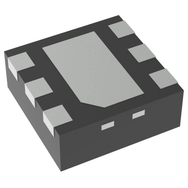
TPS62560 and TPS62562 are available in a 2-mm ×
2-mm, 6-pin SON package, whereas the TPS62561 is
available in a 5-pin SOT package.
Device Information(1)
PART NUMBER
PACKAGE
BODY SIZE (NOM)
TPS62560,
TPS62562
SON (6)
2.00 mm × 2.00 mm
TPS62561
SOT (5)
2.90 mm × 1.60 mm
(1) For all available packages, see the orderable addendum at
the end of the data sheet.
Typical Application Schematic
TPS62560DRV
VIN
CIN
L
2.2 mH
SW
R1
EN
4.7 mF
GND
MODE
C1
22 pF
Efficiency vs Output Current
Up to 600 mA
VOUT
100
COUT
90 V = 2.7 V
IN
10 mF
80 VIN = 3 V
FB
R2
Copyright © 2016, Texas Instruments Incorporated
h – Efficiency – %
VIN = 2.5 V to 5.5 V
70
60
VIN = 3.6 V
VIN = 4.5 V
50
40
30
20
10
0
0.01
VOUT = 1.8 V
MODE = GND
L = 2.2 mH
DCR 110 mR
0.1
1
10
100
IOUT – Output Current – mA
1000
1
An IMPORTANT NOTICE at the end of this data sheet addresses availability, warranty, changes, use in safety-critical applications,
intellectual property matters and other important disclaimers. PRODUCTION DATA.
�TPS62561
TPS62560, TPS62562
SLVS815D – JANUARY 2008 – REVISED OCTOBER 2016
www.ti.com
Table of Contents
1
2
3
4
5
6
7
8
Features ..................................................................
Applications ...........................................................
Description .............................................................
Revision History.....................................................
Device Comparison Table.....................................
Pin Configuration and Functions .........................
Specifications.........................................................
1
1
1
2
4
4
5
7.1
7.2
7.3
7.4
7.5
7.6
5
5
5
5
6
7
Absolute Maximum Ratings ......................................
ESD Ratings..............................................................
Recommended Operating Conditions.......................
Thermal Information ..................................................
Electrical Characteristics...........................................
Typical Characteristics ..............................................
Detailed Description .............................................. 8
8.1
8.2
8.3
8.4
Overview ................................................................... 8
Functional Block Diagram ......................................... 8
Feature Description................................................... 9
Device Functional Modes........................................ 10
9
Application and Implementation ........................ 11
9.1 Application Information............................................ 11
9.2 Typical Application ................................................. 11
9.3 System Examples .................................................. 18
10 Power Supply Recommendations ..................... 18
11 Layout................................................................... 19
11.1 Layout Guidelines ................................................. 19
11.2 Layout Examples................................................... 19
12 Device and Documentation Support ................. 21
12.1
12.2
12.3
12.4
12.5
12.6
12.7
Device Support ....................................................
Related Links ........................................................
Receiving Notification of Documentation Updates
Community Resources..........................................
Trademarks ...........................................................
Electrostatic Discharge Caution ............................
Glossary ................................................................
21
21
21
21
21
21
21
13 Mechanical, Packaging, and Orderable
Information ........................................................... 22
4 Revision History
NOTE: Page numbers for previous revisions may differ from page numbers in the current version.
Changes from Revision C (December 2009) to Revision D
Page
•
Added ESD Ratings table, Feature Description section, Device Functional Modes, Application and Implementation
section, Power Supply Recommendations section, Layout section, Device and Documentation Support section, and
Mechanical, Packaging, and Orderable Information section. ................................................................................................. 1
•
Removed Ordering Information table .................................................................................................................................... 1
•
Changed text string From ".....up to 1000-mA output current.." To ".....up to 600-mA output current.." in Description. ........ 1
•
Corrected typographical errors in Figure 32; from "VIN= 2 V to 6 V" to "VIN = 2.5 V to 5.5 V" ............................................. 18
Changes from Revision B (March 2009) to Revision C
Page
•
Deleted High Efficiency Step Down Converter....................................................................................................................... 1
•
Deleted "Wide" from Features bullet ...................................................................................................................................... 1
•
Deleted "for Li-Ion Batteries With Extended Voltage Range" from Features ........................................................................ 1
•
Deleted "Adjustable and Fixed Output-Voltage Options" from Features................................................................................ 1
•
Deleted "2.25 MHz Fixed Frequency Operation" from Features ............................................................................................ 1
•
Deleted "Power Save Mode at Light Load Currents" from Features ..................................................................................... 1
•
Deleted "Voltage Positioning at Light Loads" from Features.................................................................................................. 1
•
Deleted "Allows < 1-mm Solution Height" from Features....................................................................................................... 1
•
Changed Description to better reflect device capabilities and differences to TPS62260....................................................... 1
Changes from Revision A (July 2008) to Revision B
•
2
Page
Added TPS62562 device number........................................................................................................................................... 1
Submit Documentation Feedback
Copyright © 2008–2016, Texas Instruments Incorporated
Product Folder Links: TPS62561 TPS62560 TPS62562
�TPS62561
TPS62560, TPS62562
www.ti.com
SLVS815D – JANUARY 2008 – REVISED OCTOBER 2016
Changes from Original (January 2008) to Revision A
•
Page
Changed at all levels. Revision A is a complete rewrite of this data sheet............................................................................ 1
Copyright © 2008–2016, Texas Instruments Incorporated
Product Folder Links: TPS62561 TPS62560 TPS62562
Submit Documentation Feedback
3
�TPS62561
TPS62560, TPS62562
SLVS815D – JANUARY 2008 – REVISED OCTOBER 2016
www.ti.com
5 Device Comparison Table
(1)
(2)
Mode Pin
Output Voltage (1)
SON (6)
yes
Adjustable
CEY
SOT (5)
forced PWM only
Adjustable
CVO
SON (6)
yes
1.8 V fixed
NXT
Part Number
Package
TPS62560
TPS62561
TPS62562
Device Marking (2)
Contact TI for other fixed output voltage options
For the most current package and ordering information, see Mechanical, Packaging, and Orderable Information, or see the TI website at
www.ti.com
6 Pin Configuration and Functions
DDC Package
5-Pin SOT
Top View
VIN
1
GND
2
DRV Package
6-Pin SON
Top View
5
SW
SW
MODE
FB
EN
3
1
6
GND
2 Thermal 5
Pad
VIN
3
EN
4
FB
4
Pin Functions
PIN
No.
QFN-6
No.
TSOT23-5
I/O
DESCRIPTION
EN
4
3
I
This is the enable pin of the device. Pulling this pin to low forces the device into
shutdown mode. Pulling this pin to high enables the device. This pin must be terminated.
FB
3
4
I
Feedback pin for the internal regulation loop. Connect the external resistor divider to this
pin. In the fixed-output-voltage option, connect this terminal directly to the output
capacitor.
GND
6
2
—
MODE
2
N/A
I
This pin is only available as a QFN package option. MODE pin = high forces the device
to operate in the fixed-frequency PWM mode. MODE pin = low enables the power-save
mode with automatic transition from PFM mode to fixed-frequency PWM mode.
SW
1
5
O
This is the switch pin and is connected to the internal MOSFET switches. Connect the
external inductor between this pin and the output capacitor.
VIN
5
1
—
VIN power-supply pin
Exposed
Thermal
Pad
—
N/A
—
Must be soldered to achieve appropriate power dissipation. Should be connected to
GND.
NAME
4
Submit Documentation Feedback
GND supply pin
Copyright © 2008–2016, Texas Instruments Incorporated
Product Folder Links: TPS62561 TPS62560 TPS62562
�TPS62561
TPS62560, TPS62562
www.ti.com
SLVS815D – JANUARY 2008 – REVISED OCTOBER 2016
7 Specifications
7.1 Absolute Maximum Ratings
over operating free-air temperature range (unless otherwise noted) (1)
MIN
MAX
Input voltage range (2)
–0.3
7
Voltage range at EN, MODE
–0.3
VIN +0.3, ≤ 7
Voltage on SW
–0.3
7
Peak output current
UNIT
V
Internally limited
A
TJ
Maximum operating junction temperature
–40
125
°C
Tstg
Storage temperature
–65
150
°C
(1)
(2)
Stresses beyond those listed under absolute maximum ratings may cause permanent damage to the device. These are stress ratings
only and functional operation of the device at these or any other conditions beyond those indicated under recommended operating
conditions is not implied. Exposure to absolute-maximum-rated conditions for extended periods may affect device reliability.
All voltage values are with respect to the network ground terminal.
7.2 ESD Ratings
VALUE
V(ESD)
(1)
(2)
(3)
Electrostatic discharge (1)
Human-body model (HBM), per ANSI/ESDA/JEDEC JS-001 (2)
±2000
Charged-device model (CDM), per JEDEC specification JESD22C101 (3)
±1000
Machine model
±200
UNIT
V
The human-body model is a 100-pF capacitor discharged through a 1.5-kΩ resistor into each terminal. The machine model is a 200-pF
capacitor discharged directly into each terminal.
JEDEC document JEP155 states that 500-V HBM allows safe manufacturing with a standard ESD control process. Manufacturing with
less than 500-V HBM is possible with the necessary precautions.
JEDEC document JEP157 states that 250-V CDM allows safe manufacturing with a standard ESD control process. Manufacturing with
less than 250-V CDM is possible with the necessary precautions.
7.3 Recommended Operating Conditions
MIN
MAX
UNIT
VIN
Supply voltage
2.5
5.5
VOUT
Output voltage range for adjustable voltage
0.85
VIN
V
V
TA
Operating ambient temperature
–40
85
°C
TJ
Operating junction temperature
–40
125
°C
7.4 Thermal Information
THERMAL METRIC
(1)
TPS62560,
TPS62562
TPS62561
DRV (SON)
DDC (SOT)
6 PINS
5 PINS
UNIT
RθJA
Junction-to-ambient thermal resistance
67.8
226.9
°C/W
RθJC(top)
Junction-to-case (top) thermal resistance
88.5
40.7
°C/W
RθJB
Junction-to-board thermal resistance
37.2
48.8
°C/W
ψJT
Junction-to-top characterization parameter
2.0
0.5
°C/W
ψJB
Junction-to-board characterization parameter
37.6
48.1
°C/W
RθJC(bot)
Junction-to-case (bottom) thermal resistance
7.9
n/a
°C/W
(1)
For more information about traditional and new thermal metrics, see the Semiconductor and IC Package Thermal Metrics application
report, SPRA953.
Copyright © 2008–2016, Texas Instruments Incorporated
Product Folder Links: TPS62561 TPS62560 TPS62562
Submit Documentation Feedback
5
�TPS62561
TPS62560, TPS62562
SLVS815D – JANUARY 2008 – REVISED OCTOBER 2016
www.ti.com
7.5 Electrical Characteristics
Over full operating ambient temperature range, typical values are at TA = 25°C. Unless otherwise noted, specifications apply
for condition VIN = EN = 3.6 V. External components CIN = 4.7 μF 0603, COUT = 10 μF 0603, L = 2.2 μH
PARAMETER
TEST CONDITIONS
MIN
TYP
MAX
UNIT
SUPPLY
VIN
Input voltage range
IOUT
Output current
2.5
VIN 2.5 V to 5.5 V
IOUT = 0 mA, PFM mode enabled
(MODE = GND), device not switching
IQ
μA
18.5
(1)
IOUT = 0 mA, switching with no load
(MODE = VIN), PWM operation, VOUT = 1.8 V,
VIN = 3 V
ISD
Shutdown current
UVLO
V
mA
15
IOUT = 0 mA, PFM mode enabled
(MODE = GND), device switching, VOUT = 1.8 V, See
Operating quiescent current
5.5
600
EN = GND
Undervoltage lockout threshold
3.8
mA
0.5
μA
Falling
1.85
Rising
1.95
V
ENABLE, MODE
VIH
High-level input voltage, EN, MODE
2 V ≤ VIN ≤ 5.5 V
1
VIN
VIL
Low-level input voltage, EN, MODE
2 V ≤ VIN ≤ 5.5 V
0
0.4
V
IIN
Input bias current, EN, MODE
EN, MODE = GND or VIN
0.01
1
μA
252
492
194
391
1
1.2
V
POWER SWITCH
High side MOSFET on-resistance
RDS(on)
Low side MOSFET on-resistance
ILIMF
TSD
VIN = VGS = 3.6 V, TA = 25°C
Forward current limit, high and low side
MOSFET
VIN = VGS = 3.6 V
Thermal shutdown
Increasing junction temperature
140
Thermal-shutdown hysteresis
Decreasing junction temperature
20
Oscillator frequency
2 V ≤ VIN ≤ 5.5 V
0.8
mΩ
A
°C
OSCILLATOR
fSW
2.25
MHz
OUTPUT
VOUT
Adjustable-output voltage range
VOUT
TPS62562 fixed output voltage
Vref
Reference voltage
0.85
VIN ≥ 1.8 V
Feedback voltage, PWM mode
MODE = VIN, PWM operation, for fixed-outputvoltage versions VFB = VOUT,
2.5 V ≤ VIN ≤ 5.5 V, 0 mA ≤ IOUT ≤ 600 mA (2)
Feedback voltage, PFM mode
MODE = GND, device in PFM mode, voltage
positioning active (1)
VFB
–2.5%
VIN
V
1.8
V
600
mV
0%
2.5%
1%
Load regulation
PWM mode
–1
%/A
tStart Up
Start-up time
Time from active EN to reach 95% of VOUT nominal
500
μs
tRamp
VOUT ramp-up time
Time to ramp from 5% to 95% of VOUT
250
Ilkg
Leakage current into SW terminal
VIN = 3.6 V, VIN = VOUT = VSW, EN = GND
(1)
(2)
(3)
6
(3)
0.5
μs
1
μA
In PFM mode, the internal reference voltage is set to typ. 1.01 × Vref. See the section.
For VIN = VOUT + 0.6 V
In fixed-output-voltage versions, the internal resistor divider network is disconnected from the FB terminal.
Submit Documentation Feedback
Copyright © 2008–2016, Texas Instruments Incorporated
Product Folder Links: TPS62561 TPS62560 TPS62562
�TPS62561
TPS62560, TPS62562
www.ti.com
SLVS815D – JANUARY 2008 – REVISED OCTOBER 2016
7.6 Typical Characteristics
0.8
20
MODE == GND,
GND
MODE
EN == VIN,
VIN
EN
Device
Device Not
Not Switching
Switching
0.7
18
0.6
IQ – Quiescent Current – mA
ISD - Shutdown Current Into VIN − mA
EN = GND
o
TA = 85 C
0.5
0.4
0.3
0.2
o
TA = -40oC
TA = 25 C
16
o
C
TTAA = 25 °C
14
12
C
TTAA == –40
-40o°C
10
0.1
0
2.5
3
3.5
4
4.5
5
8
8 222
5.5
2.5
3
0.8
High-Side Switching
0.7
0.6
o
TA = 85 C
0.5
TA = 25oC
0.4
0.3
0.2
o
TA = −40 C
0.1
0
2.5
3
3.5
4
44
55
4.5
4.5
5.5
5.5
66
4.5
5
Figure 2. Quiescent Current vs Input Voltage
RDS(on) − Static Drain-Source On-State Resistance − W
Figure 1. Shutdown Current into VIN vs Input Voltage
2
3.5
V
VIN
InputVoltage
Voltage–−VV
IN–−Input
VIN − Input Voltage − V
RDS(on) − Static Drain-Source On-State Resistance − W
o
TTAA == 85
85°C
0.4
Low-Side Switching
0.35
0.3
TA = 85oC
0.25
o
TA = 25 C
0.2
0.15
0.1
o
TA = –40 C
0.05
0
2
2.5
3
3.5
4
4.5
5
VIN − Input Voltage − V
VIN − Input Voltage − V
G012
Figure 3. Static Drain-Source ON-State Resistance
Figure 4. Static Drain-Source ON-State Resistance vs Input
Voltage
Copyright © 2008–2016, Texas Instruments Incorporated
Product Folder Links: TPS62561 TPS62560 TPS62562
Submit Documentation Feedback
7
�TPS62561
TPS62560, TPS62562
SLVS815D – JANUARY 2008 – REVISED OCTOBER 2016
www.ti.com
8 Detailed Description
8.1 Overview
The TPS62560/62 step-down converters operate with typically 2.25-MHz fixed-frequency pulse-width modulation
(PWM) at moderate to heavy load currents. At light load currents, the converter can automatically enter powersave mode, and then operates in PFM mode. However, the TPS62561 operates with fixed-frequency PWM only,
also at light load conditions.
During PWM operation, the converter uses a unique fast-response voltage-mode control scheme with inputvoltage feed-forward to achieve good line and load regulation, allowing the use of small ceramic input and output
capacitors. At the beginning of each clock cycle initiated by the clock signal, the high-side MOSFET switch is
turned on. The current flows from the input capacitor via the high-side MOSFET switch through the inductor to
the output capacitor and load. During this phase, the current ramps up until the PWM comparator trips and the
control logic turns off the switch. The current-limit comparator also turns off the switch in case the current limit of
the high-side MOSFET switch is exceeded. After a dead time, which prevents shoot-through current, the low-side
MOSFET rectifier is turned on and the inductor current ramps down. The current flows from the inductor to the
output capacitor and to the load. It returns back to the inductor through the low-side MOSFET rectifier.
The next cycle is initiated by the clock signal again turning off the low-side MOSFET rectifier and turning on the
on the high-side MOSFET switch.
8.2 Functional Block Diagram
VIN
CurrentLimit Comparator
Thermal
Shutdown
VIN
Undervoltage
Lockout 1.8 V
Limit
High Side
EN
PFM Comparator
+1% Voltage positioning
Reference
0.6 V VREF
FB
VREF +1%
Gate Driver
AntiShoot-Through
Only in 2x2SON
MODE
MODE
Softstart
VOUT RAMP
CONTROL
Error Amplifier
Control
Stage
SW1
VREF
Integrator
FB
FB
Zero-Pole
Amp.
PWM
Comp.
Limit
Low Side
RI 1
RI3
RI..N
Int. Resistor
Network
Sawtooth
Generator
GND
CurrentLimit Comparator
2.25-MHz
Oscillator
GND
Copyright © 2016, Texas Instruments Incorporated
8
Submit Documentation Feedback
Copyright © 2008–2016, Texas Instruments Incorporated
Product Folder Links: TPS62561 TPS62560 TPS62562
�TPS62561
TPS62560, TPS62562
www.ti.com
SLVS815D – JANUARY 2008 – REVISED OCTOBER 2016
8.3 Feature Description
8.3.1 Dynamic Voltage Positioning
This feature reduces the voltage under/overshoots at load steps from light to heavy load and vice versa. It is
active in power-save mode and regulates the output voltage 1% higher than the nominal value. This provides
more headroom for both the voltage drop at a load step, and the voltage increase at a load throw-off.
Output voltage
Voltage Positioning
Vout +1%
PFM Comparator
threshold
Light load
PFM Mode
Vout (PWM)
moderate to heavy load
PWM Mode
Figure 5. Power Save Mode Operation With Automatic Mode Transition
8.3.2 Undervoltage Lockout
The undervoltage lockout circuit prevents the device from malfunctioning at low input voltages and from
excessive discharge of the battery and disables the output stage of the converter. The undervoltage lockout
threshold is typically 1.85 V with falling VIN.
8.3.3 Mode Selection
The MODE terminal allows mode selection between forced-PWM mode and power-save mode.
Connecting this terminal to GND enables the power-save mode with automatic transition between PWM and
PFM modes. Pulling the MODE terminal high forces the converter to operate in fixed-frequency PWM mode even
at light load currents. This allows simple filtering of the switching frequency for noise-sensitive applications. In
this mode, the efficiency is lower compared to the power-save mode during light loads.
The state of the MODE terminal can be changed during operation to allow efficient power management by
adjusting the operation mode of the converter to the specific system requirements.
8.3.4 Enable
The device is enabled by setting the EN terminal to high. During the start-up time tStart Up, the internal circuits are
settled and the soft-start circuit is activated. The EN input can be used to control power sequencing in a system
with various dc/dc converters. The EN terminal can be connected to the output of another converter, to drive the
EN terminal high to achieve a sequencing of the given supply rails. With EN = GND, the device enters shutdown
mode, in which all internal circuits are disabled. In fixed-output-voltage versions, the internal resistor divider
network is then disconnected from the FB terminal.
8.3.5 Thermal Shutdown
As soon as the junction temperature, TJ, exceeds 140°C (typical), the device goes into thermal shutdown. In this
mode, the high-side and low-side MOSFETs are turned off. The device continues its operation when the junction
temperature falls below the thermal shutdown hysteresis.
Copyright © 2008–2016, Texas Instruments Incorporated
Product Folder Links: TPS62561 TPS62560 TPS62562
Submit Documentation Feedback
9
�TPS62561
TPS62560, TPS62562
SLVS815D – JANUARY 2008 – REVISED OCTOBER 2016
www.ti.com
8.4 Device Functional Modes
8.4.1 Soft-Start
The TPS62560 has an internal soft-start circuit that controls the ramp-up of the output voltage. The output
voltage ramps up from 5% to 95% of its nominal value typically within 250 μs. This limits the inrush current into
the converter during ramp-up and prevents possible input voltage drops when a battery or high-impedance power
source is used. The soft-start circuit is enabled within the start-up time tStart Up.
8.4.2 Power-Save Mode
The power-save mode is enabled with the MODE terminal set to the low level. If the load current decreases, the
converter enters the power-save mode of operation automatically. During power-save mode, the converter skips
switching and operates with reduced frequency in PFM mode with a minimum quiescent current to maintain high
efficiency. The converter positions the output voltage typically 1% above the nominal output voltage. This voltage
positioning feature minimizes voltage drops caused by a sudden load step.
The transition from PWM mode to PFM mode occurs once the inductor current in the low-side MOSFET switch
becomes zero, which indicates discontinuous conduction mode.
During the power-save mode, the output voltage is monitored with a PFM comparator. As the output voltage falls
below the PFM comparator threshold of VOUT nominal + 1%, the device starts a PFM current pulse. The highside MOSFET switch turns on, and the inductor current ramps up. After the on-time expires, the switch is turned
off and the low-side MOSFET switch is turned on until the inductor current becomes zero.
The converter effectively delivers a current to the output capacitor and the load. If the load is below the delivered
current, the output voltage rises. If the output voltage is equal to or higher than the PFM comparator threshold,
the device stops switching and enters a sleep mode with typical 15-μA current consumption.
If the output voltage is still below the PFM comparator threshold, a sequence of further PFM current pulses is
generated until the PFM comparator threshold is reached. The converter starts switching again once the output
voltage drops below the PFM comparator threshold.
With a fast single-threshold comparator, the output-voltage ripple during PFM-mode operation can be kept small.
The PFM pulse is time controlled, which allows modifying the charge transferred to the output capacitor by the
value of the inductor. The resulting PFM output-voltage ripple and PFM frequency depend primarily on the size of
the output capacitor and the inductor value. Increasing output capacitor values and inductor values minimizes the
output ripple. The PFM frequency decreases with smaller inductor values and increases with larger values.
The PFM mode is left and PWM mode entered in case the output current can no longer be supported in PFM
mode. The power-save mode can be disabled by setting the MODE terminal to high. The converter then operates
in the fixed-frequency PWM mode.
8.4.2.1 100% Duty-Cycle Low-Dropout Operation
The device starts to enter 100% duty-cycle mode once the input voltage comes close to the nominal output
voltage. In order to maintain the output voltage, the high-side MOSFET switch is turned on 100% for one or more
cycles.
With further decreasing VIN, the high-side MOSFET switch is turned on completely. In this case, the converter
offers a low input-to-output voltage difference. This is particularly useful in battery-powered applications to
achieve longest operation time by taking full advantage of the whole battery-voltage range.
The minimum input voltage to maintain regulation depends on the load current and output voltage; and, can be
calculated as:
sp
VINmin = VOUT max + IOUT max × (RDS(on)max + RL )
where
•
•
•
•
10
IOUTmax = maximum output current plus inductor ripple current
RDS(on)max = maximum P-channel switch RDS(on)
RL = dc resistance of the inductor
VOUTmax = nominal output voltage plus maximum output voltage tolerance
Submit Documentation Feedback
(1)
Copyright © 2008–2016, Texas Instruments Incorporated
Product Folder Links: TPS62561 TPS62560 TPS62562
�TPS62561
TPS62560, TPS62562
www.ti.com
SLVS815D – JANUARY 2008 – REVISED OCTOBER 2016
Device Functional Modes (continued)
8.4.2.2 Short-Circuit Protection
The high-side and low-side MOSFET switches are short-circuit protected with maximum switch current = ILIMF.
The current in the switches is monitored by current-limit comparators. Once the current in the high-side MOSFET
switch exceeds the threshold of its current-limit comparator, it turns off and the low-side MOSFET switch is
activated to ramp down the current in the inductor and high-side MOSFET switch. The high-side MOSFET switch
can only turn on again after the current in the low-side MOSFET switch has decreased below the threshold of its
current-limit comparator.
9 Application and Implementation
NOTE
Information in the following applications sections is not part of the TI component
specification, and TI does not warrant its accuracy or completeness. TI’s customers are
responsible for determining suitability of components for their purposes. Customers should
validate and test their design implementation to confirm system functionality.
9.1 Application Information
The TPS6256x devices are high-efficiency synchronous step-down DC–DC converter featuring power-save mode
or 2.25-MHz fixed frequency operation.
9.2 Typical Application
VIN = 2.5 V to 5.5 V
TPS62560DRV
VIN
CIN
L
2.2 mH
SW
R1
EN
4.7 mF
GND
MODE
C1
22 pF
Up to 600 mA
VOUT
COUT
10 mF
FB
R2
Copyright © 2016, Texas Instruments Incorporated
Figure 6. TPS62560DRV Adjustable
9.2.1 Design Requirements
The TPS6256x is a highly integrated DC/DC converter. The output voltage is set with an external voltage divider
for the adjustable output voltage version. The output voltage is fixed to 1.8V for the TPS62562. For proper
operation a input- and output capacitor and an inductor is required. Table 2 shows the components used for the
application characteristic curves.
9.2.2 Detailed Design Procedure
9.2.2.1 Output Voltage Setting
For adjustable output voltage versions, the output voltage can be calculated by Equation 2 with the internal
reference voltage VREF = 0.6 V typically.
æ R ö
VOUT = VREF ´ ç 1+ 1 ÷
è R2 ø
(2)
To minimize the current through the feedback divider network, R2 should be 180 kΩ or 360 kΩ. The sum of R1
and R2 should not exceed ~1 MΩ, to keep the network robust against noise. An external feed-forward capacitor
C1 is required for optimum load transient response. The value of C1 should be in the range between 22 pF and
33 pF.
In case of using the fixed output voltage version (TPS62562), Vout has to be connected to the feedback pin FB.
Copyright © 2008–2016, Texas Instruments Incorporated
Product Folder Links: TPS62561 TPS62560 TPS62562
Submit Documentation Feedback
11
�TPS62561
TPS62560, TPS62562
SLVS815D – JANUARY 2008 – REVISED OCTOBER 2016
www.ti.com
Typical Application (continued)
Route the FB line away from noise sources, such as the inductor or the SW line.
9.2.2.2 Output Filter Design (inductor and Output Capacitor)
The TPS62560 is designed to operate with inductors in the range of 1.5 μH to 4.7 μH and with output capacitors
in the range of 4.7 μF to 22 μF. The part is optimized for operation with a 2.2-μH inductor and 10-μF output
capacitor.
Larger or smaller inductor values can be used to optimize the performance of the device for specific operation
conditions. For stable operation, the L and C values of the output filter may not fall below 1 μH effective
inductance and 3.5 μF effective capacitance.
9.2.2.2.1 Inductor Selection
The inductor value has a direct effect on the ripple current. The selected inductor must be rated for its dc
resistance and saturation current. The inductor ripple current (ΔIL) decreases with higher inductance and
increases with higher VIN or VOUT.
The inductor selection also impacts the output voltage ripple in PFM mode. Higher inductor values lead to lower
output voltage ripple and higher PFM frequency; lower inductor values lead to a higher output voltage ripple but
lower PFM frequency.
Equation 3 calculates the maximum inductor current in PWM mode under static load conditions. The saturation
current of the inductor should be rated higher than the maximum inductor current as calculated with Equation 4.
This is recommended because during heavy load transients the inductor current rises above the calculated
value.
V
1 * OUT
V
DI L + VOUT
L
I L max + I out max )
IN
f
DI L
(3)
2
where
•
•
•
•
f = Switching frequency (2.25 MHz, typical)
L = Inductor value
ΔIL = Peak-to-peak inductor ripple current
ILmax = Maximum inductor current
(4)
A more conservative approach is to select the inductor current rating just for the switch current limit ILIMF of the
converter.
Accepting larger values of ripple current allows the use of lower inductance values, but results in higher output
voltage ripple, greater core losses, and lower output current capability.
The total losses of the coil have a strong impact on the efficiency of the dc/dc conversion and consist of both the
losses in the dc resistance (R(DC)) and the following frequency-dependent components:
• The losses in the core material (magnetic hysteresis loss, especially at high switching frequencies)
• Additional losses in the conductor from the skin effect (current displacement at high frequencies)
• Magnetic field losses of the neighboring windings (proximity effect)
• Radiation losses
12
Submit Documentation Feedback
Copyright © 2008–2016, Texas Instruments Incorporated
Product Folder Links: TPS62561 TPS62560 TPS62562
�TPS62561
TPS62560, TPS62562
www.ti.com
SLVS815D – JANUARY 2008 – REVISED OCTOBER 2016
Table 1. List of Inductors
(1)
DIMENSIONS, mm
INDUCTANCE, μH
INDUCTOR TYPE
SUPPLIER (1)
2,5 × 2 × 1 max
2
MIPS2520D2R2
FDK
2,5 × 2 × 1,2 max
2
MIPSA2520D2R2
FDK
2,5 × 2 × 1 max
2.2
KSLI-252010AG2R2
Hitachi Metals
2,5 × 2 × 1,2 max
2.2
LQM2HPN2R2MJ0L
Murata
3 × 3 × 1,5 max
2.2
LPS3015 2R2
Coilcraft
See Third-Party Products Disclaimer
9.2.2.2.2 Output Capacitor Selection
The advanced fast-response voltage-mode control scheme of the TPS62560 allows the use of tiny ceramic
capacitors. Ceramic capacitors with low ESR values have the lowest output voltage ripple and are
recommended. The output capacitor requires either an X7R or X5R dielectric. Y5V and Z5U dielectric capacitors,
aside from their wide variation in capacitance over temperature, become resistive at high frequencies.
At nominal load current, the device operates in PWM mode, and the RMS ripple current is calculated by
Equation 5:
V
1 - OUT
VIN
1
IRMSCOUT = VOUT ´
´
L´f
2 3
(5)
At nominal load current, the device operates in PWM mode, and the overall output voltage ripple is the sum of
the voltage spike caused by the output capacitor ESR plus the voltage ripple caused by charging and discharging
the output capacitor shown in Equation 6:
V
1 - OUT
æ
ö
VIN
1
DVOUT = VOUT ´
´ç
+ ESR ÷
L´f
è 8 ´ COUT ´ f
ø
(6)
At light load currents, the converter operates in power-save mode, and the output voltage ripple is dependent on
the output capacitor and inductor values. Larger output capacitor and inductor values minimize the voltage ripple
in PFM mode and tighten dc output accuracy in PFM mode.
9.2.2.2.3 Input Capacitor Selection
An input capacitor is required for best input voltage filtering and minimizing the interference with other circuits
caused by high input voltage spikes. For most applications, a 4.7-μF to 10-μF ceramic capacitor is
recommended. Because a ceramic capacitor loses up to 80% of its initial capacitance at 5 V, it is recommended
that 10-μF input capacitors be used for input voltages > 4.5 V. The input capacitor can be increased without any
limit for better input voltage filtering. Take care when using only small ceramic input capacitors. When a ceramic
capacitor is used at the input and the power is being supplied through long wires, such as from a wall adapter, a
load step at the output or VIN step on the input can induce ringing at the VIN terminal. This ringing can couple to
the output and be mistaken as loop instability or could even damage the part by exceeding the maximum ratings.
Table 2. List of Capacitors (1)
(1)
CAPACITANCE
TYPE
SIZE
SUPPLIER
4.7 μF
GRM188R60J475K
0603—1,6 × 0,8 × 0,8 mm
Murata
10 μF
GRM188R60J106M69D
0603—1,6 × 0,8 × 0,8 mm
Murata
See Third-Party Products Disclaimer
Copyright © 2008–2016, Texas Instruments Incorporated
Product Folder Links: TPS62561 TPS62560 TPS62562
Submit Documentation Feedback
13
�TPS62561
TPS62560, TPS62562
SLVS815D – JANUARY 2008 – REVISED OCTOBER 2016
www.ti.com
9.2.3 Application Curves
100
100
90
90
VIN = 2.7 V
80
VIN = 2.7 V
VIN = 3.6 V
70
h – Efficiency – %
h – Efficiency – %
80 V = 3 V
IN
VIN = 4.5 V
60
50
40
30
10
0
0.01
VIN = 3 V
60
VIN = 3.6 V
VIN = 4.5 V
50
40
30
VOUT = 1.8 V
MODE = GND
L = 2.2 mH
DCR 110 mR
20
70
VOUT = 1.8 V
MODE = VIN
L = 2.2 mH
20
10
0
0.1
1
10
100
1000
1
10
100
IOUT – Output Current – mA
IOUT – Output Current – mA
1000
G003
G002
Figure 8. Efficiency vs Output Current
Figure 7. Efficiency vs Output Current
100
100
VIN = 4.2 V
90
80
60
h – Efficiency – %
VIN = 5 V
VIN = 4.5 V
50
40
VOUT = 3.3 V
MODE = VIN
L = 2.2 mH
DCR 110 mW
COUT = 10 mF 0603
30
20
10
VIN = 3.6 V
VIN = 5 V
10
100
IOUT – Output Current – mA
70
VIN = 4.5 V
60
50
40
VOUT = 3.3 V
MODE = GND
L = 2.2 mH
DCR = 110 mH
COUT = 10 mF 0603
30
20
10
0
0.01
0
1
VIN = 4.2 V
80
VIN = 3.6 V
70
h – Efficiency – %
90
1000
0.1
1
10
100
1000
IOUT – Output Current – mA
Figure 9. Efficiency vs Output Current
Figure 10. Efficiency vs Output Current
100
100
90
90
VIN = 2.7 V
80
80
60
h − Efficiency − %
h − Efficiency − %
VIN = 4.5 V
70
VIN = 4.5 V
50
VIN = 3.6 V
40
VOUT = 1.2 V
MODE = VIN
L = 2 mH
MIPSA2520
COUT = 10 mF 0603
30
20
10
10
100
VIN = 3.6 V
60
50
VIN = 2.7 V
40
30
VOUT = 1.2 V
MODE = GND
L = 2 mH
MIPSA2520
COUT = 10 mF 0603
20
10
0
1
70
1000
IOUT − Output Current − mA
0
0.01
0.1
Submit Documentation Feedback
10
100
1000
G005
G004
Figure 11. Efficiency vs Output Current
14
1
IOUT − Output Current − mA
Figure 12. Efficiency vs Output Current
Copyright © 2008–2016, Texas Instruments Incorporated
Product Folder Links: TPS62561 TPS62560 TPS62562
�TPS62561
TPS62560, TPS62562
www.ti.com
SLVS815D – JANUARY 2008 – REVISED OCTOBER 2016
VIN 3.6V
VOUT 1.8V, IOUT 150mA
L 2.2mH, COUT 10mF 0603
VOUT 10 mV/Div
VIN = 3.6 V
VOUT = 1.8 V
IOUT = 10 mA
MODE
2V/Div
SW 2 V/Div
SW
2V/Div
PFM Mode
Forced PWM Mode
ICOIL 200 mA/Div
Icoil
200mA/Div
Time Base - 1 ms/Div
Time Base - 10 ms/Div
Figure 13. Typical Operation - PWM Mode
MODE
2 V/Div
VIN = 3.6 V
VOUT = 1.8 V
IOUT = 10 mA
SW
2 V/Div
Figure 14. Mode Pin Transition from PFM to FORCED PWM
Mode at Light Load
EN 2 V/Div
VIN = 3.6 V
RLoad = 10 Ω
VOUT = 1.8 V
IIN into CIN
MODE = GND
SW 2 V/Div
PFM Mode
Forced PWM Mode
VOUT 2 V/Div
ICOIL
200 mA/Div
IIN 100 mA/Div
Time Base - 100 ms/Div
Time Base - 2.5 ms/Div
Figure 15. Mode Pin Transition from PWM to PFM MODE at
Light Load
VOUT 50 mV/Div
VIN 3.6 V
VOUT 1.5 V
IOUT 50 mA to 200 mA
MODE = VIN
Figure 16. Start-UP Timing
VIN 3.6 V
VOUT 1.5 V
IOUT 200 mA to 400 mA
VOUT 50 mV/Div
IOUT 200 mA/Div
400 mA
200 mA
IOUT 200 mA/Div
ICOIL 500 mA/Div
ICOIL 500 mA/Div
Time Base - 20 ms/Div
Figure 17. Forced PWM Load Transient
Time Base - 20 ms/Div
Figure 18. Forced PWM Load Transient
Copyright © 2008–2016, Texas Instruments Incorporated
Product Folder Links: TPS62561 TPS62560 TPS62562
Submit Documentation Feedback
15
�TPS62561
TPS62560, TPS62562
SLVS815D – JANUARY 2008 – REVISED OCTOBER 2016
www.ti.com
SW 2 V/Div
SW 2 V/Div
VIN 3.6 V
VOUT 1.5 V
IOUT 150 mA to 400 mA
VOUT 50mV/Div
MODE = GND
VIN 3.6 V
VOUT 1.5 V
IOUT 150 mA to 400 mA
MODE = GND
VOUT 50 mV/Div
400 mA
IOUT 500 mA/Div
400 mA
IOUT 500 mA/Div
150 mA
150 mA
ICOIL500 mA/Div
ICOILl 500mA/Div
Time Base – 500 ms/Div
Figure 19. PFM Load Transient
Time Base – 500 ms/Div
Figure 20. PFM Load Transient
SW 2 V/Div
VIN 3.6 V
VOUT 1.5 V
IOUT 1.5 mA to 50 mA
MODE = GND
SW 2 V/Div
VIN 3.6 V
VOUT 1.5 V
IOUT 50 mA to 1.5mA
MODE = GND
VOUT 50 mV/Div
VOUT 50mV/Div
50 mA
50 mA
IOUT 50 mA/Div
IOUT 50 mA/Div
1.5 mA
1.5 mA
ICOIL 500 mA/Div
ICOIL 500 mA/Div
Time Base – 50 ms/Div
Time Base – 50 ms/Div
Figure 21. PFM Load Transient
SW 2 V/Div
Figure 22. PFM Load Transient
SW 2 V/Div
VIN 3.6 V
VOUT 1.5 V
IOUT 50 mA to 400 mA
MODE = GND
VOUT 50 mV/Div
VIN 3.6 V
VOUT 1.8 V
IOUT 50 mA to 250 mA
MODE = GND
VOUT 50 mV/Div
250 mA
IOUT 500 mA/Div
IOUT 200 mA/Div
50 mA
400 mA
50 mA
ICOIL 500 mA/Div
ICOIL 500mA/Div
Time Base – 20 ms/Div
Figure 23. PFM Load Transient
16
PWM Mode
PFM Mode
Submit Documentation Feedback
Time Base – 20 ms/Div
Figure 24. PFM Load Transient
Copyright © 2008–2016, Texas Instruments Incorporated
Product Folder Links: TPS62561 TPS62560 TPS62562
�TPS62561
TPS62560, TPS62562
www.ti.com
SLVS815D – JANUARY 2008 – REVISED OCTOBER 2016
SW 2 V/Div
VIN 3.6V to 4.2V
500 mV/Div
VIN 3.6 V
VOUT 1.5 V
IOUT 50 mA to 400 mA
MODE = GND
VOUT 50 mV/Div
PFM Mode
PWM Mode
400 mA
IOUT 500 mA/Div
VOUT = 1.8 V
50 mV/Div
IOUT = 50 mA
MODE = GND
50 mA
ICOIL 500 mA/Div
Time Base – 20 ms/Div
Time Base – 100 ms/Div
Figure 26. PFM Line Transient
Figure 25. PFM Load Transient
VOUT 20 mV/Div
VIN 3.6V to 4.2V
500 mV/Div
SW 2 V/Div
VOUT = 1.8 V
50 mV/Div
IOUT = 250 mA
MODE = GND
ICOIL 200 mA/Div
Time Base – 10 ms/Div
Time Base – 100ms/Div
Figure 28. Typical Operation - PFM Mode
Figure 27. PWM Line Transient
VIN 3.6 V; VOUT 1.8 V, IOUT 10 mA,
L = 4.7 mH, COUT = 10 mF 0603,
MODE = GND
VOUT 20 mV/Div
SW 2 V/Div
ICOIL 200 mA/Div
Time Base – 2 ms/Div
Figure 29. Typical Operation - PFM Mode
Copyright © 2008–2016, Texas Instruments Incorporated
Product Folder Links: TPS62561 TPS62560 TPS62562
Submit Documentation Feedback
17
�TPS62561
TPS62560, TPS62562
SLVS815D – JANUARY 2008 – REVISED OCTOBER 2016
www.ti.com
9.3 System Examples
TPS62560DRV
VIN = 2.5 V to 5.5 V
VIN
CIN
4.7 mF
VOUT = 1.2 V
SW
R1
360 kW
EN
GND
L1
2.2 mH
C1
22 pF
COUT
10 mF
FB
R2
360 kW
MODE
S0364_01
Copyright © 2016, Texas Instruments Incorporated
Figure 30. TPS62560 Adjustable 1.2-V Output
TPS62560DRV
VIN = 2.5 V to 5.5 V
VIN
CIN
4.7 mF
VOUT = 1.5 V
Up to 600 mA
SW
R1
540 kW
EN
GND
L1
2.2 mH
C1
22 pF
COUT
10 mF
FB
R2
360 kW
MODE
S0365-01
Copyright © 2016, Texas Instruments Incorporated
Figure 31. TPS62560 Adjustable 1.5-V Output
TPS62562DRV
VIN = 2.5 V to 5.5 V
VIN
CIN
4.7 mF
L1
2.2 mH
VOUT = 1.8 V
Up to 600 mA
SW
COUT
10 mF
EN
GND
FB
MODE
S0366-01
Copyright © 2016, Texas Instruments Incorporated
Figure 32. TPS62562 Fixed 1.8-V Output
10 Power Supply Recommendations
The TPS6226x device has no special requirements for its input power supply. The input power supply output
current must be rated according to the supply voltage, output voltage, and output current of the TPS6226x.
18
Submit Documentation Feedback
Copyright © 2008–2016, Texas Instruments Incorporated
Product Folder Links: TPS62561 TPS62560 TPS62562
�TPS62561
TPS62560, TPS62562
www.ti.com
SLVS815D – JANUARY 2008 – REVISED OCTOBER 2016
11 Layout
11.1 Layout Guidelines
As for all switching power supplies, the layout is an important step in the design. Proper function of the device
demands careful attention to PCB layout. Take care in board layout to get the specified performance. If the
layout is not carefully done, the regulator could show poor line and/or load regulation, stability issues as well as
EMI problems. It is critical to provide a low inductance, impedance ground path. Therefore, use wide and short
traces for the main current paths. The input capacitor should be placed as close as possible to the IC pins as
well as the inductor and output capacitor.
Connect the GND pin of the device to the exposed thermal pad of the PCB and use this pad as a star point. Use
a common power GND node and a different node for the signal GND to minimize the effects of ground noise.
Connect these ground nodes together to the exposed thermal pad (star point) underneath the IC. Keep the
common path to the GND pin, which returns the small signal components and the high current of the output
capacitors as short as possible to avoid ground noise. The FB line should be connected right to the output
capacitor and routed away from noisy components and traces (for example, the SW line).
11.2 Layout Examples
Figure 33. Suggested Layout for Fixed-Output-Voltage Options
Copyright © 2008–2016, Texas Instruments Incorporated
Product Folder Links: TPS62561 TPS62560 TPS62562
Submit Documentation Feedback
19
�TPS62561
TPS62560, TPS62562
SLVS815D – JANUARY 2008 – REVISED OCTOBER 2016
www.ti.com
Layout Examples (continued)
VOUT
R2
GND
C1
R1
COUT
CIN
VIN
L
G
N
D
U
Figure 34. Suggested Layout for Adjustable-Output-Voltage Version
20
Submit Documentation Feedback
Copyright © 2008–2016, Texas Instruments Incorporated
Product Folder Links: TPS62561 TPS62560 TPS62562
�TPS62561
TPS62560, TPS62562
www.ti.com
SLVS815D – JANUARY 2008 – REVISED OCTOBER 2016
12 Device and Documentation Support
12.1 Device Support
12.1.1 Third-Party Products Disclaimer
TI'S PUBLICATION OF INFORMATION REGARDING THIRD-PARTY PRODUCTS OR SERVICES DOES NOT
CONSTITUTE AN ENDORSEMENT REGARDING THE SUITABILITY OF SUCH PRODUCTS OR SERVICES
OR A WARRANTY, REPRESENTATION OR ENDORSEMENT OF SUCH PRODUCTS OR SERVICES, EITHER
ALONE OR IN COMBINATION WITH ANY TI PRODUCT OR SERVICE.
12.2 Related Links
The table below lists quick access links. Categories include technical documents, support and community
resources, tools and software, and quick access to sample or buy.
Table 3. Related Links
PARTS
PRODUCT FOLDER
SAMPLE & BUY
TECHNICAL
DOCUMENTS
TOOLS &
SOFTWARE
SUPPORT &
COMMUNITY
TPS62560
Click here
Click here
Click here
Click here
Click here
TPS62561
Click here
Click here
Click here
Click here
Click here
TPS62562
Click here
Click here
Click here
Click here
Click here
12.3 Receiving Notification of Documentation Updates
To receive notification of documentation updates, navigate to the device product folder on ti.com. In the upper
right corner, click on Alert me to register and receive a weekly digest of any product information that has
changed. For change details, review the revision history included in any revised document.
12.4 Community Resources
The following links connect to TI community resources. Linked contents are provided "AS IS" by the respective
contributors. They do not constitute TI specifications and do not necessarily reflect TI's views; see TI's Terms of
Use.
TI E2E™ Online Community TI's Engineer-to-Engineer (E2E) Community. Created to foster collaboration
among engineers. At e2e.ti.com, you can ask questions, share knowledge, explore ideas and help
solve problems with fellow engineers.
Design Support TI's Design Support Quickly find helpful E2E forums along with design support tools and
contact information for technical support.
12.5 Trademarks
E2E is a trademark of Texas Instruments.
All other trademarks are the property of their respective owners.
12.6 Electrostatic Discharge Caution
These devices have limited built-in ESD protection. The leads should be shorted together or the device placed in conductive foam
during storage or handling to prevent electrostatic damage to the MOS gates.
12.7 Glossary
SLYZ022 — TI Glossary.
This glossary lists and explains terms, acronyms, and definitions.
Copyright © 2008–2016, Texas Instruments Incorporated
Product Folder Links: TPS62561 TPS62560 TPS62562
Submit Documentation Feedback
21
�TPS62561
TPS62560, TPS62562
SLVS815D – JANUARY 2008 – REVISED OCTOBER 2016
www.ti.com
13 Mechanical, Packaging, and Orderable Information
The following pages include mechanical, packaging, and orderable information. This information is the most
current data available for the designated devices. This data is subject to change without notice and revision of
this document. For browser-based versions of this data sheet, refer to the left-hand navigation.
22
Submit Documentation Feedback
Copyright © 2008–2016, Texas Instruments Incorporated
Product Folder Links: TPS62561 TPS62560 TPS62562
�PACKAGE OPTION ADDENDUM
www.ti.com
14-Oct-2022
PACKAGING INFORMATION
Orderable Device
Status
(1)
Package Type Package Pins Package
Drawing
Qty
Eco Plan
(2)
Lead finish/
Ball material
MSL Peak Temp
Op Temp (°C)
Device Marking
(3)
Samples
(4/5)
(6)
TPS62560DRVR
ACTIVE
WSON
DRV
6
3000
RoHS & Green
NIPDAU
Level-1-260C-UNLIM
-40 to 85
CEY
Samples
TPS62560DRVT
ACTIVE
WSON
DRV
6
250
RoHS & Green
NIPDAU
Level-1-260C-UNLIM
-40 to 85
CEY
Samples
TPS62561DDCR
ACTIVE
SOT-23-THIN
DDC
5
3000
RoHS & Green
NIPDAU
Level-1-260C-UNLIM
-40 to 85
CVO
Samples
TPS62561DDCT
ACTIVE
SOT-23-THIN
DDC
5
250
RoHS & Green
NIPDAU
Level-1-260C-UNLIM
-40 to 85
CVO
Samples
TPS62562DRVR
ACTIVE
WSON
DRV
6
3000
RoHS & Green
NIPDAU
Level-1-260C-UNLIM
-40 to 85
NXT
Samples
TPS62562DRVT
ACTIVE
WSON
DRV
6
250
RoHS & Green
NIPDAU
Level-1-260C-UNLIM
-40 to 85
NXT
Samples
(1)
The marketing status values are defined as follows:
ACTIVE: Product device recommended for new designs.
LIFEBUY: TI has announced that the device will be discontinued, and a lifetime-buy period is in effect.
NRND: Not recommended for new designs. Device is in production to support existing customers, but TI does not recommend using this part in a new design.
PREVIEW: Device has been announced but is not in production. Samples may or may not be available.
OBSOLETE: TI has discontinued the production of the device.
(2)
RoHS: TI defines "RoHS" to mean semiconductor products that are compliant with the current EU RoHS requirements for all 10 RoHS substances, including the requirement that RoHS substance
do not exceed 0.1% by weight in homogeneous materials. Where designed to be soldered at high temperatures, "RoHS" products are suitable for use in specified lead-free processes. TI may
reference these types of products as "Pb-Free".
RoHS Exempt: TI defines "RoHS Exempt" to mean products that contain lead but are compliant with EU RoHS pursuant to a specific EU RoHS exemption.
Green: TI defines "Green" to mean the content of Chlorine (Cl) and Bromine (Br) based flame retardants meet JS709B low halogen requirements of


 工商网监
湘ICP备2023018690号
工商网监
湘ICP备2023018690号
