TPS63000-Q1
www.ti.com ...................................................................................................................................................................................................... SLVS968 – JUNE 2009
HIGH-EFFICIENCY SINGLE INDUCTOR BUCK-BOOST CONVERTER WITH 1.8-A SWITCH
FEATURES
1
• Qualified for Automotive Applications
• Up to 96% Efficiency
• 1200-mA Output Current at 3.3 V in Step Down
Mode (VIN = 3.6 V to 5.5 V)
• Up to 800-mA Output Current at 3.3 V in Boost
Mode (VIN > 2.4 V)
• Automatic Transition between Step Down and
Boost Mode
• Device Quiescent Current Less Than 50 µA
• Input Voltage Range: 1.8 V to 5.5 V
• Adjustable Output Voltage From 1.2 V to 5.5 V
• Power Save Mode for Improved Efficiency at
Low Output Power
• Forced Fixed Frequency Operation and
Synchronization Possible
•
•
•
23
Load Disconnect During Shutdown
Over-Temperature Protection
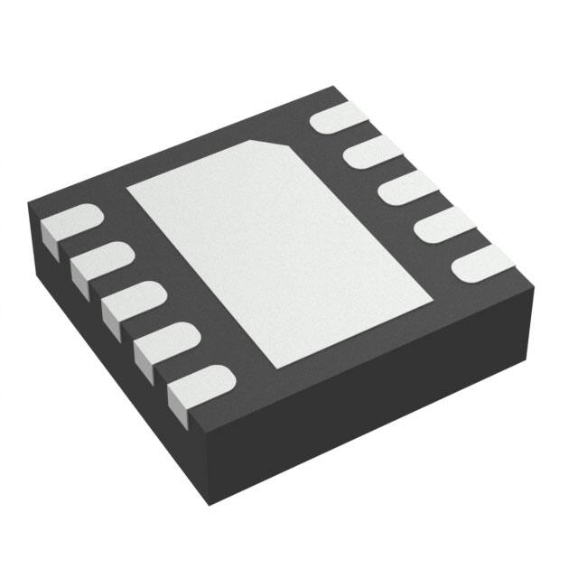
Available in Small 3 mm × 3 mm, QFN-10
Package
APPLICATIONS
•
All Two-Cell and Three-Cell Alkaline, NiCd or
NiMH or Single-Cell Li Battery Powered
Products
Portable Audio Players
PDAs
Cellular Phones
Personal Medical Products
White LEDs
•
•
•
•
•
DESCRIPTION
The TPS63000 devices provide a power supply solution for products powered by either a two-cell or three-cell
alkaline, NiCd or NiMH battery, or a one-cell Li-Ion or Li-polymer battery. Output currents can go as high as 1200
mA while using a single-cell Li-Ion or Li-Polymer battery, and discharge it down to 2.5 V or lower. The buck-boost
converter is based on a fixed frequency, pulse-width-modulation (PWM) controller using synchronous rectification
to obtain maximum efficiency. At low load currents, the converter enters Power Save mode to maintain high
efficiency over a wide load current range. The Power Save mode can be disabled, forcing the converter to
operate at a fixed switching frequency. The maximum average current in the switches is limited to a typical value
of 1800 mA. The output voltage is programmable using an external resistor divider. The converter can be
disabled to minimize battery drain. During shutdown, the load is disconnected from the battery. The device is
packaged in a 10-pin QFN PowerPAD™ package measuring 3 mm × 3 mm (DRC).
L1
2.2µH
L1
VIN
1.8V to
5.5V
L2
VIN
C1
10µF
VOUT
VINA
EN
FB
C2
10µF
VOUT
3.3V up to
1200mA
PS/SYNC
GND
PGND
TPS63000
1
2
3
Please be aware that an important notice concerning availability, standard warranty, and use in critical applications of Texas
Instruments semiconductor products and disclaimers thereto appears at the end of this data sheet.
PowerPAD is a trademark of Texas Instruments.
All other trademarks are the property of their respective owners.
PRODUCTION DATA information is current as of publication date.
Products conform to specifications per the terms of the Texas
Instruments standard warranty. Production processing does not
necessarily include testing of all parameters.
Copyright © 2009, Texas Instruments Incorporated
�TPS63000-Q1
SLVS968 – JUNE 2009 ...................................................................................................................................................................................................... www.ti.com
These devices have limited built-in ESD protection. The leads should be shorted together or the device placed in conductive foam
during storage or handling to prevent electrostatic damage to the MOS gates.
ORDERING INFORMATION (1)
PACKAGE (2)
TA
–40°C to 85°C
(1)
(2)
QFN – DRC
Reel of 3000
ORDERABLE PART NUMBER
TPS63000IDRCRQ1
TOP-SIDE MARKING
ODJ
For the most current package and ordering information, see the Package Option Addendum at the end of this document, or see the TI
web site at www.ti.com.
Package drawings, thermal data, and symbolization are available at www.ti.com/packaging.
ABSOLUTE MAXIMUM RATINGS
over operating free-air temperature range (unless otherwise noted) (1)
Input voltage range on VIN, VINA, L1, L2, VOUT, PS/SYNC, EN, FB
–0.3 V to 7 V
Operating virtual junction temperature range, TJ
–40°C to 150°C
Storage temperature range Tstg
–65°C to 150°C
(1)
Stresses beyond those listed under absolute maximum ratings may cause permanent damage to the device. These are stress ratings
only, and functional operation of the device at these or any other conditions beyond those indicated under recommended operating
conditions is not implied. Exposure to absolute-maximum-rated conditions for extended periods my affect device reliability.
DISSIPATION RATINGS TABLE
PACKAGE
THERMAL RESISTANCE
θJA
POWER RATING
TA ≤ 25°C
DERATING FACTOR ABOVE
TA = 25°C
DRC
48.7°C/W
2054 mW
21 mW/°C
RECOMMENDED OPERATING CONDITIONS
MIN
MAX
UNIT
VI
Input voltage
1.8
5.5
V
VI
Input voltage for startup
1.9
5.5
V
VO
Output voltage
1.2
5.5
V
TA
Operating free air temperature
–40
85
°C
TJ
Operating virtual junction temperature
–40
125
°C
2
Submit Documentation Feedback
Copyright © 2009, Texas Instruments Incorporated
Product Folder Link(s): TPS63000-Q1
�TPS63000-Q1
www.ti.com ...................................................................................................................................................................................................... SLVS968 – JUNE 2009
ELECTRICAL CHARACTERISTICS
over recommended free-air temperature range and over recommended input voltage range (typical at an ambient temperature
range of 25°C) (unless otherwise noted)
PARAMETER
TEST CONDITIONS
MIN
TYP
495
500
MAX
UNIT
DC/DC Stage
VFB
Feedback voltage
f
Oscillator frequency
1250
Frequency range for synchronization
ISW
1250
Switch current limit
VIN = VINA = 3.6 V, TA = 25°C
1600
High-side switch on resistance
VIN = VINA = 3.6 V
100
Low-side switch on resistance
VIN = VINA = 3.6 V
100
1800
kHz
2100
mΩ
Load regulation
0.5%
Quiescent
current
IO = 0 mA, VEN = VIN = VINA = 3.6 V,
VOUT = 3.3 V
VINA
Shutdown current
VEN = 0 V, VIN = VINA = 3.6 V
mA
mΩ
0.5%
VOUT (adjustable output voltage)
IS
mV
kHz
Line regulation
VIN
Iq
1800
505
1500
1
1.5
µA
40
50
µA
4
6
µA
0.1
1
µA
1.7
1.8
V
0.4
V
0.1
µA
Control Stage
VUVLO
Undervoltage lockout threshold
VIL
EN, PS/SYNC input low voltage
VIH
EN, PS/SYNC input high voltage
EN, PS/SYNC input current
VINA voltage decreasing
1.5
1.2
Clamped on GND or VINA
V
0.01
Overtemperature protection
140
°C
Overtemperature hysteresis
20
°C
Submit Documentation Feedback
Copyright © 2009, Texas Instruments Incorporated
Product Folder Link(s): TPS63000-Q1
3
�TPS63000-Q1
SLVS968 – JUNE 2009 ...................................................................................................................................................................................................... www.ti.com
PIN ASSIGNMENTS
DRC PACKAGE
(TOP VIEW)
VOUT
1
10
L2
PGND
L1
VIN
2
4
Exposed 9
Thermal 8
Pad
7
5
6
3
FB
GND
VINA
PS/SYNC
EN
Terminal Functions
TERMINAL
NAME
NO.
I/O
DESCRIPTION
EN
6
I
Enable input. 1 = enabled, 0 = disabled
FB
10
I
Voltage feedback of adjustable version
GND
9
PS/SYNC
7
I
Enable / disable power save mode. 1 = disabled, = 0 enabled. Clock signal for synchronization.
L1
4
I
Connection for inductor
L2
2
I
Connection for inductor
PGND
3
VIN
5
I
Supply voltage for power stage
VOUT
1
O
Buck-boost converter output
VINA
8
I
Supply voltage for control stage
Thermal Pad
4
Control / logic ground
Power ground
Must be soldered to the PCB to achieve appropriate power dissipation. Connect to PGND.
Submit Documentation Feedback
Copyright © 2009, Texas Instruments Incorporated
Product Folder Link(s): TPS63000-Q1
�TPS63000-Q1
www.ti.com ...................................................................................................................................................................................................... SLVS968 – JUNE 2009
FUNCTIONAL BLOCK DIAGRAM
L1
L2
VIN
VOUT
Current
Sensor
VBAT
VOUT
PGND PGND
Gate
Control
_
VINA
Modulator
PS/SYNC
Oscillator
+
+
_
FB
VREF
+
-
Device
Control
EN
Temperature
Control
PGND
PGND
GND
Submit Documentation Feedback
Copyright © 2009, Texas Instruments Incorporated
Product Folder Link(s): TPS63000-Q1
5
�TPS63000-Q1
SLVS968 – JUNE 2009 ...................................................................................................................................................................................................... www.ti.com
TYPICAL CHARACTERISTICS
MAXIMUM OUTPUT CURRENT
vs
INPUT VOLTAGE
1800
VO = 1.8 V
IO - Maximum Output Current - mA
1600
1400
1200
1000
800
600
400
200
0
1.8
2.6
5
4.2
3.4
VI - Input Voltage - V
Figure 1.
STARTUP AFTER ENABLE
(VOUT = 2.5 V)
Enable
2 V/div,dc
Output Voltage
1 V/div,dc
Inductor Current
200 mA/div,dc
Voltage at L1
2 V/div, dc
TPS63000,
VO = 2.5 V
VI = 3.3 V, IO = 300 mA
Timebase 50 ms/div
Figure 2.
6
Submit Documentation Feedback
Copyright © 2009, Texas Instruments Incorporated
Product Folder Link(s): TPS63000-Q1
�TPS63000-Q1
www.ti.com ...................................................................................................................................................................................................... SLVS968 – JUNE 2009
PARAMETER MEASUREMENT INFORMATION
L1
L2
L1
VIN
VIN
C1
R3
VINA
R1
EN
C2
FB
PS/SYNC
C3
VOUT
VOUT
GND
R2
PGND
TPS63000
List of Components
REFERENCE
DESCRIPTION
MANUFACTURER
TPS63000
Texas Instruments
L1
VLF4012-2R2
TDK
C1
10 µF, 6.3 V, 0603, X7R ceramic
C2
2 × 10 µF, 6.3 V, 0603, X7R ceramic
C3
0.1 µF, X7R ceramic
R3
100 Ω
R1, R2
Depending on the output voltage
Submit Documentation Feedback
Copyright © 2009, Texas Instruments Incorporated
Product Folder Link(s): TPS63000-Q1
7
�TPS63000-Q1
SLVS968 – JUNE 2009 ...................................................................................................................................................................................................... www.ti.com
DETAILED DESCRIPTION
Controller Circuit
The controlling circuit of the device is based on an average current mode topology. The average inductor current
is regulated by a fast current regulator loop which is controlled by a voltage control loop. The controller also uses
input and output voltage feed forward. Changes of input and output voltage are monitored and immediately can
change the duty cycle in the modulator to achieve a fast response to those errors. The voltage error amplifier
gets its feedback input from the FB pin, and a resistive voltage divider must be connected to that pin. The
feedback voltage is compared with the internal reference voltage to generate a stable and accurate output
voltage.
The controller circuit also senses the average input current as well as the peak input current. With this, maximum
input power can be controlled as well as the maximum peak current to achieve a safe and stable operation under
all possible conditions. To finally protect the device from overheating, an internal temperature sensor is
implemented.
Synchronous Operation
The device uses four internal N-channel MOSFETs to maintain synchronous power conversion at all possible
operating conditions. This enables the device to keep high efficiency over a wide input voltage and output power
range.
To avoid ground shift problems due to the high currents in the switches, two separate ground pins GND and
PGND are used. The reference for all control functions is the GND pin. The power switches are connected to
PGND. Both grounds must be connected on the PCB at only one point ideally close to the GND pin. Due to the
4-switch topology, the load is always disconnected from the input during shutdown of the converter.
Buck-Boost Operation
To be able to regulate the output voltage properly at all possible input voltage conditions, the device
automatically switches from step down operation to boost operation and back as required by the configuration. It
always uses one active switch, one rectifying switch, one switch permanently on, and one switch permanently off.
Therefore, it operates as a step down converter (buck) when the input voltage is higher than the output voltage,
and as a boost converter when the input voltage is lower than the output voltage. There is no mode of operation
in which all 4 switches are permanently switching. Controlling the switches this way allows the converter to
maintain high efficiency at the most important point of operation; when input voltage is close to the output
voltage. The RMS current through the switches and the inductor is kept at a minimum, to minimize switching and
conduction losses. Switching losses are also kept low by using only one active and one passive switch.
Regarding the remaining 2 switches, one is kept permanently on and the other is kept permanently off, thus
causing no switching losses.
Power Save Mode and Synchronization
The PS/SYNC pin can be used to select different operation modes. To enable power save, PS/SYNC must be
set low. Power save mode is used to improve efficiency at light load. If power save mode is enabled, the
converter stops operating if the average inductor current gets lower than about 300 mA and the output voltage is
at or above its nominal value. If the output voltage decreases below its nominal value, the device ramps up the
output voltage again by starting operation using a programmed average inductor current higher than required by
the current load condition. Operation can last for one or several pulses. The converter again stops operating
once the conditions for stopping operation are met again.
The power save mode can be disabled by programming high at the PS/SYNC. Connecting a clock signal at
PS/SYNC forces the device to synchronize to the connected clock frequency. Synchronization is done by a PLL,
so synchronizing to lower and higher frequencies compared to the internal clock works without any issues. The
PLL can also tolerate missing clock pulses without the converter malfunctioning. The PS/SYNC input supports
standard logic thresholds.
8
Submit Documentation Feedback
Copyright © 2009, Texas Instruments Incorporated
Product Folder Link(s): TPS63000-Q1
�TPS63000-Q1
www.ti.com ...................................................................................................................................................................................................... SLVS968 – JUNE 2009
Device Enable
The device is put into operation when EN is set high. It is put into a shutdown mode when EN is set to GND. In
shutdown mode, the regulator stops switching, all internal control circuitry is switched off, and the load is
disconnected from the input. This also means that the output voltage can drop below the input voltage during
shutdown. During start-up of the converter, the duty cycle and the peak current are limited in order to avoid high
peak currents flowing from the input.
Soft Start and Short-Circuit Protection
After being enabled, the device starts operating. The average current limit ramps up from an initial 400 mA
following the output voltage increasing. At an output voltage of about 1.2 V, the current limit is at its nominal
value. If the output voltage does not increase, the current limit will not increase. There is no timer implemented.
Thus the output voltage overshoot at startup, as well as the inrush current, is kept at a minimum. The device
ramps up the output voltage in a controlled manner even if a very large capacitor is connected at the output.
When the output voltage does not increase above 1.2 V, the device assumes a short circuit at the output and
keeps the current limit low to protect itself and the application. At a short at the output during operation the
current limit also will be decreased accordingly. At 0 V at the output, for example, the output current will not
exceed about 400 mA.
Undervoltage Lockout
An undervoltage lockout function prevents device start-up if the supply voltage on VINA is lower than
approximately its threshold (see electrical characteristics table). When in operation, the device automatically
enters the shutdown mode if the voltage on VINA drops below the undervoltage lockout threshold. The device
automatically restarts if the input voltage recovers to the minimum operating input voltage.
Overtemperature Protection
The device has a built-in temperature sensor which monitors the internal IC temperature. If the temperature
exceeds the programmed threshold (see electrical characteristics table) the device stops operating. As soon as
the IC temperature has decreased below the programmed threshold, it starts operating again. There is a built-in
hysteresis to avoid unstable operation at IC temperatures at the overtemperature threshold.
Submit Documentation Feedback
Copyright © 2009, Texas Instruments Incorporated
Product Folder Link(s): TPS63000-Q1
9
�TPS63000-Q1
SLVS968 – JUNE 2009 ...................................................................................................................................................................................................... www.ti.com
APPLICATION INFORMATION
Design Procedure
The TPS63000 dc/dc converters are intended for systems powered by one-cell Li-Ion or Li-Polymer battery with a
typical voltage between 2.3 V and 4.5 V. They can also be used in systems powered by a double or triple cell
Alkaline, NiCd, or NiMH battery with a typical terminal voltage between 1.8 V and 5.5 V . Additionally, any other
voltage source with a typical output voltage between 1.8 V and 5.5 V can power systems where the TPS63000 is
used.
Programming the Output Voltage
An external resistor divider is used to adjust the output voltage. The resistor divider must be connected between
VOUT, FB, and GND. When the output voltage is regulated properly, the typical value of the voltage at the FB
pin is 500 mV. The maximum recommended value for the output voltage is 5.5 V. The current through the
resistive divider should be about 100 times greater than the current into the FB pin. The typical current into the
FB pin is 0.01 µA, and the voltage across the resistor between FB and GND, R2, is typically 500 mV. Based on
those two values, the recommended value for R2 should be lower than 500 kΩ, in order to set the divider current
at 1 µA or higher. It is recommended to keep the value for this resistor in the range of 200 kΩ. From that, the
value of the resistor connected between VOUT and FB, R1, depending on the needed output voltage (VOUT), can
be calculated using Equation 1:
R 1 + R2
ǒ
VOUT
V FB
Ǔ
*1
(1)
If as an example, an output voltage of 3.3 V is needed, a 1.0-MΩ resistor should be chosen for R1. To improve
control performance, using a feed-forward capacitor in parallel to R1 is recommended. The value for the
feed-forward capacitor can be calculated using Equation 2.
2.2 ms
C ff +
R1
(2)
L1
L1
VIN
L2
VIN
C1
R3
VINA
R1
EN
C3
C2
FB
PS/SYNC
GND
VOUT
VOUT
R2
PGND
TPS6300X
Figure 3. Typical Application Circuit for Adjustable Output Voltage Option
10
Submit Documentation Feedback
Copyright © 2009, Texas Instruments Incorporated
Product Folder Link(s): TPS63000-Q1
�TPS63000-Q1
www.ti.com ...................................................................................................................................................................................................... SLVS968 – JUNE 2009
Inductor Selection
To properly configure the TPS63000 devices, an inductor must be connected between pin L1 and pin L2. To
estimate the inductance value Equation 3 and Equation 4 can be used.
L1 +
L2 +
ǒVIN1 * VOUTǓ
VOUT
V IN1
Vin2
f
0.3 A
(3)
ǒVOUT * VIN2Ǔ
V OUT
f
0.3 A
(4)
In both equations f is the minimum switching frequency. In Equation 3 the minimum inductance value, L1 for step
down mode operation is calculated. VIN1 is the maximum input voltage. In Equation 4 the minimum inductance,
L2, for boost mode operation is calculated. VIN2 is the minimum input voltage. The recommended minimum
inductor value is either L1 or L2 whichever is higher. As an example, a suitable inductor for generating 3.3 V from
a Li-Ion battery with a battery voltage range from 2.5 V up to 4.2 V is 2.2 µH. The recommended inductor value
range is between 1.5 µH and 4.7 µH. In general, this means that at high voltage conversion rates, higher inductor
values offer better performance.
With the chosen inductance value, the peak current for the inductor in steady state operation can be calculated.
Equation 5 shows how to calculate the peak current I1 in step down mode operation and Equation 6 shows how
to calculate the peak current I2 in boost mode operation.
VOUTǒV IN1 * V OUTǓ
I
I 1 + OUT )
0.8
2 V IN1 f L
V
I OUT VIN2
I 2 + OUT
)
2
0.8 V IN2
(5)
ǒV OUT * V IN2Ǔ
VOUT
f
L
(6)
The critical current value for selecting the right inductor is the higher value of I1 and I2. It also needs to be taken
into account that load transients and error conditions may cause higher inductor currents. This also needs to be
taken into account when selecting an appropriate inductor. The following inductor series from different suppliers
have been used with TPS63000 converters:
Table 1. List of Inductors
VENDOR
Coilcraft
INDUCTOR SERIES
LPS3015
LPS4012
Murata
LQH3NP
Tajo Yuden
NR3015
TDK
VLF3215
VLF4012
Capacitor Selection
Input Capacitor
At least a 4.7 µF input capacitor is recommended to improve transient behavior of the regulator and EMI
behavior of the total power supply circuit. A ceramic capacitor placed as close as possible to the VIN and PGND
pins of the IC is recommended.
Submit Documentation Feedback
Copyright © 2009, Texas Instruments Incorporated
Product Folder Link(s): TPS63000-Q1
11
�TPS63000-Q1
SLVS968 – JUNE 2009 ...................................................................................................................................................................................................... www.ti.com
Output Capacitor
For the output capacitor, it is recommended to use small ceramic capacitors placed as close as possible to the
VOUT and PGND pins of the IC. If, for any reason, the application requires the use of large capacitors which can
not be placed close to the IC, using a smaller ceramic capacitor in parallel to the large one is recommended.
This small capacitor should be placed as close as possible to the VOUT and PGND pins of the IC.
To get an estimate of the recommended minimum output capacitance, Equation 7 can be used.
mF
C OUT + 5 L
mH
(7)
A capacitor with a value in the range of the calculated minimum should be used. This is required to maintain
control loop stability. There are no additional requirements regarding minimum ESR. There is also no upper limit
for the output capacitance value. Larger capacitors will cause lower output voltage ripple as well as lower output
voltage drop during load transients.
Layout Considerations
As for all switching power supplies, the layout is an important step in the design, especially at high peak currents
and high switching frequencies. If the layout is not carefully done, the regulator could show stability problems as
well as EMI problems. Therefore, use wide and short traces for the main current path and for the power ground
tracks. The input capacitor, output capacitor, and the inductor should be placed as close as possible to the IC.
Use a common ground node for power ground and a different one for control ground to minimize the effects of
ground noise. Connect these ground nodes at any place close to one of the ground pins of the IC.
The feedback divider should be placed as close as possible to the control ground pin of the IC. To lay out the
control ground, it is recommended to use short traces as well, separated from the power ground traces. This
avoids ground shift problems, which can occur due to superimposition of power ground current and control
ground current.
Thermal Information
Implementation of integrated circuits in low-profile and fine-pitch surface-mount packages typically requires
special attention to power dissipation. Many system-dependent issues such as thermal coupling, airflow, added
heat sinks and convection surfaces, and the presence of other heat-generating components affect the
power-dissipation limits of a given component.
Three basic approaches for enhancing thermal performance are listed below.
• Improving the power dissipation capability of the PCB design
• Improving the thermal coupling of the component to the PCB by soldering the Thermal Pad
• Introducing airflow in the system
The maximum recommended junction temperature (TJ) of the TPS63000 devices is 125°C. The thermal
resistance of the 10-pin QFN 3 × 3 package (DRC) is RθJA = 48.7°C/W, if the thermal pad is soldered. Specified
regulator operation is assured to a maximum ambient temperature TA of 85°C. Therefore, the maximum power
dissipation is about 820 mW, as calculated in Equation 8. More power can be dissipated if the maximum ambient
temperature of the application is lower.
T
*T
J(MAX)
A
P
+
+ 125°C * 85°C + 820 mW
D(MAX)
R
48.7 °CńW
qJA
(8)
12
Submit Documentation Feedback
Copyright © 2009, Texas Instruments Incorporated
Product Folder Link(s): TPS63000-Q1
�PACKAGE OPTION ADDENDUM
www.ti.com
10-Dec-2020
PACKAGING INFORMATION
Orderable Device
Status
(1)
Package Type Package Pins Package
Drawing
Qty
Eco Plan
(2)
Lead finish/
Ball material
MSL Peak Temp
Op Temp (°C)
Device Marking
(3)
(4/5)
(6)
TPS63000IDRCRQ1
ACTIVE
VSON
DRC
10
3000
RoHS & Green
NIPDAU
Level-3-260C-168 HR
-40 to 125
ODJ
(1)
The marketing status values are defined as follows:
ACTIVE: Product device recommended for new designs.
LIFEBUY: TI has announced that the device will be discontinued, and a lifetime-buy period is in effect.
NRND: Not recommended for new designs. Device is in production to support existing customers, but TI does not recommend using this part in a new design.
PREVIEW: Device has been announced but is not in production. Samples may or may not be available.
OBSOLETE: TI has discontinued the production of the device.
(2)
RoHS: TI defines "RoHS" to mean semiconductor products that are compliant with the current EU RoHS requirements for all 10 RoHS substances, including the requirement that RoHS substance
do not exceed 0.1% by weight in homogeneous materials. Where designed to be soldered at high temperatures, "RoHS" products are suitable for use in specified lead-free processes. TI may
reference these types of products as "Pb-Free".
RoHS Exempt: TI defines "RoHS Exempt" to mean products that contain lead but are compliant with EU RoHS pursuant to a specific EU RoHS exemption.
Green: TI defines "Green" to mean the content of Chlorine (Cl) and Bromine (Br) based flame retardants meet JS709B low halogen requirements of


 工商网监
湘ICP备2023018690号
工商网监
湘ICP备2023018690号
