TPS63900
TPS63900
SLVSET3D – MARCH 2020 – REVISED OCTOBER
2020
SLVSET3D – MARCH 2020 – REVISED OCTOBER 2020
www.ti.com
TPS63900 1.8-V to 5.5-V, 75-nA IQ Buck-boost Converter with Input Current Limit and
DVS
1 Features
3 Description
•
•
The TPS63900 device is a high-efficiency
synchronous buck-boost converter with an extremely
low quiescent current (75 nA typical). The device has
32 user-programmable output voltage settings from
1.8 V to 5 V.
•
•
•
•
•
Input voltage range: 1.8 V to 5.5 V
Output voltage range: 1.8 V to 5 V (100-mV steps)
– Programmable with external resistors
– SEL pin to toggle between two output voltage
presets
> 400-mA output current for VI ≥ 2.0 V, VO = 3.3 V
(typical 1.45-A peak switching current limit)
– Stackable: parallel multiple devices for higher
output current
> 90% Efficiency at 10-µA load current
– 75-nA quiescent current
– 60-nA shutdown current
Single-mode operation
– Eliminates mode transitions between buck,
buck-boost and boost operation
– Low output ripple
– Excellent transient performance
Safety and robust operation features
– Integrated soft start
– Programmable input current limit with eight
settings (1 mA to 100 mA and unlimited)
– Output short-circuit and overtemperature
protection
Tiny solution size of 21-mm2
– Small 2.2-µH inductor, single 22-µF output
capacitor
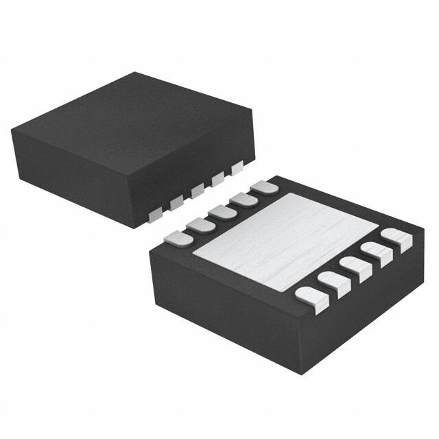
– 10-Pin, 2.5-mm × 2.5-mm, 0.5-mm pitch WSON
package
A dynamic voltage-scaling feature lets applications
switch between two output voltages during operation;
for example, to save power by using a lower system
supply voltage during standby operation.
With its wide supply voltage range and programmable
input current limit (1 mA to 100 mA and unlimited), the
device is ideal for use with a wide range of primary
like 3S Alkaline, 1S Li-MnO 2 or 1S Li-SOCl 2, and
secondary battery types.
The
high-output
current
capability
supports
commonly-used RF standards like sub-1-GHz, BLE,
LoRa, wM-Bus, and NB-IoT.
Device Information
PART NUMBER(1)
PACKAGE
BODY SIZE (NOM)
TPS63900
WSON (10)
2.5 mm × 2.5 mm
(1)
For all available packages, see the orderable addendum at
the end of the data sheet.
2.2 µH
VI
1.8 V to 5.5 V
10 µF
2 Applications
•
•
•
•
•
•
Smart meters and sensor nodes
Electronic smart locks
Medical sensor patches and patient monitors
Wearable electronics
Asset tracking
Industrial IoT (smart sensors) / NB-IoT
LX1
VIN
SEL
EN
LX2
VO
1.8 V to 5.0 V
VOUT
22 µF
TPS63900
GND
CFG1
CFG2
CFG3
Simplified Schematic
An IMPORTANT NOTICE at the end of this data sheet addresses availability, warranty, changes, use in safety-critical applications,
Submit Document Feedback
Copyright
© 2020 Texas
Instruments
Incorporated
intellectual
property
matters
and other important disclaimers. PRODUCTION DATA.
Product Folder Links: TPS63900
1
�TPS63900
www.ti.com
SLVSET3D – MARCH 2020 – REVISED OCTOBER 2020
Table of Contents
1 Features............................................................................1
2 Applications..................................................................... 1
3 Description.......................................................................1
4 Revision History.............................................................. 2
5 Pin Configuration and Functions...................................3
6 Specifications.................................................................. 4
6.1 Absolute Maximum Ratings ....................................... 4
6.2 ESD Ratings .............................................................. 4
6.3 Recommended Operating Conditions ........................4
6.4 Thermal Information ...................................................4
6.5 Electrical Characteristics ............................................5
6.6 Typical Characteristics................................................ 7
7 Detailed Description........................................................8
7.1 Overview..................................................................... 8
7.2 Functional Block Diagram........................................... 8
7.3 Feature Description.....................................................8
7.4 Device Functional Modes..........................................17
8 Application and Implementation.................................. 18
8.1 Application Information............................................. 18
8.2 Typical Application.................................................... 18
9 Power Supply Recommendations................................30
10 Layout...........................................................................31
10.1 Layout Guidelines................................................... 31
10.2 Layout Example...................................................... 31
11 Device and Documentation Support..........................32
11.1 Device Support........................................................32
11.2 Documentation Support.......................................... 32
11.3 Receiving Notification of Documentation Updates.. 32
11.4 Support Resources................................................. 32
11.5 Trademarks............................................................. 32
11.6 Electrostatic Discharge Caution.............................. 32
11.7 Glossary.................................................................. 32
12 Mechanical, Packaging, and Orderable
Information.................................................................... 32
4 Revision History
NOTE: Page numbers for previous revisions may differ from page numbers in the current version.
Changes from Revision C (September 2020) to Revision D (October 2020)
Page
• Changed device status from Advance Information to Production Data.............................................................. 1
2
Submit Document Feedback
Copyright © 2020 Texas Instruments Incorporated
Product Folder Links: TPS63900
�TPS63900
www.ti.com
SLVSET3D – MARCH 2020 – REVISED OCTOBER 2020
5 Pin Configuration and Functions
EN
1
10
VIN
SEL
2
9
LX1
CFG1
3
8
GND
CFG2
4
7
LX2
CFG3
5
6
VOUT
Thermal
Pad
Not to scale
Figure 5-1. 10-Pin WSON DSK Package (Top View)
Table 5-1. Pin Functions
PIN
I/O
DESCRIPTION
EN
I
Device enable. A high level applied to this pin enables the device and a low level disables it.
It must not be left open.
2
SEL
I
Output voltage select. Selects VO(2) when a high level is applied to this pin. Selects VO(1)
when a low level is applied to this pin. It must not be left open.
3
CFG1
I
Configuration pin 1. Connect a resistor between this pin and ground to set VO(2) and input
current limit, must not be left open.
4
CFG2
I
Configuration pin 2. Connect a resistor between this pin and ground to set VO(2) and input
current limit. Must not be left open.
5
CFG3
I
Configuration pin 3. Connect a resistor between this pin and ground to set VO(1). Must not be
left open.
6
VOUT
—
NO.
NAME
1
Output voltage
7
LX2
—
Switching node of the boost stage
8
GND
—
Ground
9
LX1
—
Switching node of the buck stage
10
VIN
—
Supply voltage
—
Thermal Pad
—
Connect this pin to ground for correct operation.
Submit Document Feedback
Copyright © 2020 Texas Instruments Incorporated
Product Folder Links: TPS63900
3
�TPS63900
www.ti.com
SLVSET3D – MARCH 2020 – REVISED OCTOBER 2020
6 Specifications
6.1 Absolute Maximum Ratings
over operating junction temperature range (unless otherwise noted)
(1)
(2)
VI
Input voltage (VIN, LX1, LX2, VOUT, EN, CFG1, CFG2, CFG3, SEL)
MIN
MAX
–0.3
5.9
UNIT
V
TJ
Operating junction temperature
–40
150
°C
Tstg
Storage temperature
–65
150
°C
(1)
(2)
Stresses beyond those listed under Absolute Maximum Ratings may cause permanent damage to the device. These are stress ratings
only, which do not imply functional operation of the device at these or any other conditions beyond those indicated under
Recommended Operating Conditions. Exposure to absolute-maximum-rated conditions for extended periods may affect device
reliability.
All voltage values are with respect to network ground terminal, unless otherwise noted.
6.2 ESD Ratings
VALUE
Human body model (HBM), per ANSI/ESDA/JEDEC
V(ESD)
(1)
(2)
Electrostatic discharge
JS-001(1)
UNIT
±2000
Charged-device model (CDM), per JEDEC specification JESD22-C101
or ANSI/ESDA/JEDEC JS-002(2)
V
±750
JEDEC document JEP155 states that 500-V HBM allows safe manufacturing with a standard ESD control process.
JEDEC document JEP157 states that 250-V CDM allows safe manufacturing with a standard ESD control process.
6.3 Recommended Operating Conditions
over operating free-air temperature range (unless otherwise noted)
MIN
VI
NOM
MAX
UNIT
Supply voltage
1.8
5.5
V
VO
Output voltage
1.8
5.0
V
IO
Output current (VI ≥ 2.0 V, VO = 3.6 V)
0.4
A
A)(1)
CI
Input capacitance (VI = 2.5 V to 5 V, VO = 3.3 V, IO = 0.4
CO
Output capacitance (VI = 2.5 V to 5 V, VO = 3.3 V, IO = 0.4 A)(1)
C(CFG)
Capacitance (CFG1, CFG2, CFG3)
L
Inductance
ISAT
Inductor saturation current rating
5
µF
10
µF
10
2.2
Unlimited current setting
2
≤100-mA current settings
1
pF
µH
A
TA
Operating ambient temperature
–40
85
°C
TJ
Operating junction temperature
–40
125
°C
(1)
Effective capacitance after DC bias effects have been considered.
6.4 Thermal Information
TPS63900
THERMAL METRIC(1)
DSK Package
(WSON)
UNIT
10 PINS
4
RθJA
Junction-to-ambient thermal resistance
64.6
°C/W
RθJC(top)
Junction-to-case (top) thermal resistance
62.3
°C/W
RθJB
Junction-to-board thermal resistance
31.1
°C/W
ψJT
Junction-to-top characterization parameter
1.6
°C/W
Submit Document Feedback
Copyright © 2020 Texas Instruments Incorporated
Product Folder Links: TPS63900
�TPS63900
www.ti.com
SLVSET3D – MARCH 2020 – REVISED OCTOBER 2020
TPS63900
DSK Package
(WSON)
THERMAL METRIC(1)
UNIT
10 PINS
ψJB
Junction-to-board characterization parameter
31.0
°C/W
RθJC(bot)
Junction-to-case (bottom) thermal resistance
10.0
°C/W
(1)
For more information about traditional and new thermal metrics, see the Semiconductor and IC Package Thermal Metrics application
report, SPRA953.
6.5 Electrical Characteristics
Over operating junction temperature range and recommended supply voltage range (unless otherwise noted). Typical values
are at VI = 3.0 V, VO = 2.5 V and TJ = 25°C (unless otherwise noted).
PARAMETER
TEST CONDITIONS
MIN
TYP
MAX
0.075
1
UNIT
SUPPLY
Quiescent current into VIN
V(EN) = 3 V, no load, not switching,
"unlimited" current setting
Shutdown current into VIN
V(EN) = 0 V
VIT+(UVLO)
Positive-going UVLO threshold voltage
Vhys(UVLO)
UVLO threshold voltage hysteresis
VIT+(POR)
Positive-going POR threshold voltage
60
µA
nA
1.73
1.75
1.77
V
90
100
110
mV
1.74
V
1.37
I/O SIGNALS
VIH
High-level input voltage (EN, SEL)
VIL
Low-level input voltage (EN, SEL)
1.2
0.4
V(EN), V(SEL) = 1.8 V or 0 V.
TJ = 25°C
Input current (EN, SEL)
V
V
±1
±10
nA
POWER SWITCH
VI = 3 V, VO = 5 V,
test current = 1 A
155
Q2
VI = 3 V, VO = 3 V, test current = 1 A
110
Q3
VI = 3 V, VO = 3 V,
test current = 1 A
110
Q4
VI = 5 V, VO = 3 V,
test current = 1 A
155
Q1
rDS(on)
On-state resistance
mΩ
CURRENT LIMIT
Peak current limit during Startup (Q1)
Peak current limit (Q1)
VI = 3.6 V,
unlimited current limit setting
0.35
VI = 1.8 V, VO = 3.6 V,
unlimited current limit setting
1.33
VI = 3.6 V, VO = 3.3 V,
100-mA current limit setting
0.15
1-mA setting
2.5-mA setting
5-mA setting
Average input current limit
TJ = –40°C to
85°C
0.83
1.45
0.29
A
1.6
A
0.51
1
2.5
5
10-mA settting
10
25-mA setting
25
50-mA setting
50
100-mA setting
100
mA
OUTPUT
Output voltage DC accuracy
IO = 1 mA, CO(eff) = 10 µF, L(eff) = 2.2
µH
±1.5
%
Submit Document Feedback
Copyright © 2020 Texas Instruments Incorporated
Product Folder Links: TPS63900
5
�TPS63900
www.ti.com
SLVSET3D – MARCH 2020 – REVISED OCTOBER 2020
Over operating junction temperature range and recommended supply voltage range (unless otherwise noted). Typical values
are at VI = 3.0 V, VO = 2.5 V and TJ = 25°C (unless otherwise noted).
PARAMETER
TEST CONDITIONS
MIN
TYP
MAX
UNIT
CONTROL
Internal reference resistor
33
R2D setting #0
RCFG
kΩ
0
0.1
R2D setting #1
–3%
0.511
+3%
R2D setting #2
–3%
1.15
+3%
R2D setting #3
–3%
1.87
+3%
R2D setting #4
–3%
2.74
+3%
R2D setting #5
–3%
3.83
+3%
R2D setting #6
–3%
5.11
+3%
R2D setting #7
–3%
6.49
+3%
R2D setting #8
–3%
8.25
+3%
R2D setting #9
–3%
10.5
+3%
R2D setting #10
–3%
13.3
+3%
R2D setting #11
–3%
16.2
+3%
R2D setting #12
–3%
20.5
+3%
R2D setting #13
–3%
24.9
+3%
R2D setting #14
–3%
30.1
+3%
R2D setting #15
–3%
36.5
+3%
Thermal shutdown threshold
temperature
140
150
160
°C
Thermal shutdown hysteresis
15
20
25
°C
kΩ
PROTECTION FEATURES
TIMING PARAMETERS
6
td(POR)
POR signal delay after reaching POR
threshold
td(EN)
Delay between a rising edge on the EN
Supply voltage stable before EN pin
pin and the start of the output voltage
goes high
ramp
tw(SS)
Soft-start step duration
td(SEL)
Delay between a change in the state of
the SEL pin and the first step change in
the output voltage
tw(DVS)
Dynamic voltage scaling step duration
td(RESTART)
Restart delay after protection
3.8
VO > 1.8 V
100
100
Submit Document Feedback
ms
1.5
ms
125
150
µs
30
40
µs
125
150
µs
10
11
ms
Copyright © 2020 Texas Instruments Incorporated
Product Folder Links: TPS63900
�TPS63900
www.ti.com
SLVSET3D – MARCH 2020 – REVISED OCTOBER 2020
6.6 Typical Characteristics
0.4
0.375
0.275
0.225
0.175
0.125
0.075
0.025
1.8
VO = 5.1 V
-40 qC
25 qC
85 qC
0.35
Quiescent Current (PA)
Quiescent Current (PA)
0.325
-40 qC
25 qC
85 qC
0.3
0.25
0.2
0.15
0.1
0.05
2.3
2.8
3.3
3.8
VIN (V)
EN = HIGH
4.3
4.8
0
1.8
5.3
IO = 0 mA, device
not switching
2.3
VO = 5.1 V
Figure 6-1. Quiescent Current into VIN versus
Input Voltage
2.8
3.3
3.8
VIN (V)
EN = HIGH
4.3
4.8
5.3
IO = 0 mA, device
not switching
Figure 6-2. Quiescent Current into VOUT versus
Input Voltage
0.375
Shutdown Current (PA)
0.325
-40 qC
25 qC
85 qC
0.275
0.225
0.175
0.125
0.075
0.025
1.8
2.3
2.8
3.3
3.8
VIN (V)
4.3
VO = 5.1 V
4.8
5.3
EN = LOW
Figure 6-3. Shutdown Current versus Input Voltage
Submit Document Feedback
Copyright © 2020 Texas Instruments Incorporated
Product Folder Links: TPS63900
7
�TPS63900
www.ti.com
SLVSET3D – MARCH 2020 – REVISED OCTOBER 2020
7 Detailed Description
7.1 Overview
The TPS63900 device is a four-switch synchronous buck-boost converter with a maximum output current of 400
mA. It has a single-mode operation that allows the device to regulate the output voltage to a level above, below,
or equal to the input voltage without displaying the mode-switching transients and unpredictable inductor current
ripple from which many other buck-boost devices suffer.
The switching frequency of the TPS63900 device varies with the operating conditions: it is lowest when IO is low
and increases smoothly as IO increases.
EN
LX2
LX1
7.2 Functional Block Diagram
Enable
(to all blocks)
&
UVLO
tIL(PEAK)t
State
Machine
Reference
Voltage
tVreft
Power
Stage
VOUT
Control
Block
tIL(VALLEY)t
tNÂ9Ot
Input
Current
Limit
Attenuator
Output
Voltage
VIN
R2D Interface
SEL
CFG3
CFG2
CFG1
GND
7.3 Feature Description
7.3.1 Trapezoidal Current Control
Figure 7-1 shows a simplified block diagram of the power stage of the device. Inductor current is sensed in
series with Q1 (the peak current) and Q4 (the valley current).
8
Submit Document Feedback
Copyright © 2020 Texas Instruments Incorporated
Product Folder Links: TPS63900
�TPS63900
www.ti.com
SLVSET3D – MARCH 2020 – REVISED OCTOBER 2020
IL(PEAK)
IL(VALLEY)
Q1
L
CI
Q4
Q2
Q3
CO
Figure 7-1. Power Stage Simplified Block Diagram
The device uses a trapezoidal inductor current to regulate its output under all operating conditions. Thus, the
device only has one operating mode and does not display any of the mode-change transients or unpredictable
switching displayed by many other buck-boost devices.
There are four phases of operation:
•
•
•
•
Phase A – Q1 and Q3 are on and Q2 and Q4 are off
Phase B – Q1 and Q4 are on and Q2 and Q3 are off
Phase C – Q2 and Q4 are on and Q1 and Q3 are off
Phase D – Q2 and Q3 are on and Q1 and Q4 are off
Figure 7-2 shows the inductor current waveform when V I > V O, Figure 7-3 shows the current waveform when V I
= VO, and Figure 7-4 shows the current waveform when VI < VO.
Phase D
Phase C
Phase B
IL(PEAK)
Phase A
Inductor Current
Figure 7-2 through Figure 7-4 show the typical waveforms during continuous conduction mode (CCM) switching
for three operating conditions. During discontinuous conduction mode (DCM), the typical inductor current
waveforms look similar to CCM with Phase D at 0 A inductor current. In deep boost mode, where V I VO (CCM)
IL(VALLEY)
0
Time
Figure 7-3. Inductor Current Waveform when VI = VO (CCM)
Submit Document Feedback
Copyright © 2020 Texas Instruments Incorporated
Product Folder Links: TPS63900
9
�TPS63900
www.ti.com
Phase D
Phase C
Phase B
IL(PEAK)
Phase A
Inductor Current
SLVSET3D – MARCH 2020 – REVISED OCTOBER 2020
IL(VALLEY)
0
Time
Figure 7-4. Inductor Current Waveform when VI < VO (CCM)
The ideal relationship between VI and VO (that is, assuming no losses) is
VO = VI F
tw:A; + tw(B)
G
tw(B) + tw(C)
(1)
where
•
•
•
•
•
VI is the input voltage
VO is the output voltage
tw(A) is the duration of phase A
tw(B) is the duration of phase B
tw(C) is the duration of phase C
By varying relative duration of each phase, the device can regulate V O to be less than, equal to, or greater than
VI.
7.3.2 Device Enable / Disable
The device turns on when all the following conditions are true:
•
•
The supply voltage is greater than the positive-going undervoltage lockout (UVLO) threshold.
The EN pin is high.
The device turns off when at least one of the following conditions is true:
•
•
The supply voltage is less than the negative-going UVLO threshold.
The EN pin is low.
A complete state diagram is shown in Figure 7-13.
After the device turns on, the internal reference system starts, then the trimming information and the CFG pins
are read out. The device ignores any further changes to the CFG pins during device operation.
Figure 7-5 shows the internal start-up sequence.
10
Submit Document Feedback
Copyright © 2020 Texas Instruments Incorporated
Product Folder Links: TPS63900
�TPS63900
www.ti.com
SLVSET3D – MARCH 2020 – REVISED OCTOBER 2020
VI
VIT+(POR)
EN
ttr(SS)t
td(POR)
ttd(EN)t
ttlim(SS)t
ttramp(SS)t
Internal
Sequence
VO
Power-on
reset
Start internal
reference system
Read trim bits
Read CFG pins
1.2 V
Figure 7-5. Internal Start-Up Sequence
7.3.3 Soft Start
The device has a soft-start feature that starts the device typically with 500-mA peak current limit until VO = 1.8 V
and 500 µs elapsed when the input current limit is set to unlimited (see Section 7.3.4). Afterwards, the output
voltage ramps in a series of discrete steps (see Figure 7-6).
•
•
When VO ≤ 1.8 V, peak current is limited to 500 mA typical for 500 µs.
When VO > 1.8 V, each step is 100 mV high and has a duration of 125 µs.
The total soft-start ramp-up time can be calculated with Equation 2.
tr(SS) = VO × 1.25 BmsWVC - 1.75>ms?
(2)
where
•
•
tr(SS) is the rise time of the output voltage in milliseconds
VO is the output voltage in volts
Figure 7-6 shows a typical start-up case.
EN
VIH
ttd(EN)t
Internal ramp
ttr(SS)t
Target voltage
Output
Voltage
0V
Figure 7-6. Start-Up Behavior
Figure 7-7 illustrates the start-up step size behavior.
t125 µst
1.8 V
t100 mVt
Output
Voltage
t500 µst
Figure 7-7. Typical Soft-Start Ramp Step Size
Submit Document Feedback
Copyright © 2020 Texas Instruments Incorporated
Product Folder Links: TPS63900
11
�TPS63900
www.ti.com
SLVSET3D – MARCH 2020 – REVISED OCTOBER 2020
Table 7-1 shows the typical start-up time for a number of standard output voltages.
Table 7-1. Typical Start-Up Times
OUTPUT VOLTAGE
SOFT-START RAMP- START-UP TIME (t
UP TIME (tr(SS))
d(EN) + tr(SS))
1.8 V
0.5 ms
2 ms
2.5 V
1.375 ms
2.875 ms
3.3 V
2.375 ms
3.875 ms
5V
4.5 ms
6 ms
If the output is prebiased – that is, the initial output voltage is not zero – the start-up behavior is as follows:
•
•
If the prebias voltage is lower than the target voltage, the device does not start switching until the ramping
output voltage is greater than the prebias voltage (see Figure 7-8).
If the prebias voltage is higher than the target voltage, the device does not start to switch until the output
voltage has decreased to the target voltage (see Figure 7-9). The device cannot actively discharge the output
to the target voltage and relies on the load current to discharge the output capacitor and decrease the output
voltage to the target value.
EN
VIH
ttd(EN)t
Internal ramp
ttr(SS)t
Target voltage
Output
Voltage
Prebias voltage
Device not switching
Device switching
Figure 7-8. Start-Up Behavior into Prebiased (Low) Output
EN
VIH
ttd(EN)t
Internal ramp
ttr(SS)t
Prebias voltage
Output
Voltage
Target voltage
Device not switching
Device switching
Figure 7-9. Start-Up Behavior into Prebiased (High) Output
7.3.4 Input Current Limit
The device can limit the current drawn from its supply, so that it can be used with batteries that do not support
high peak currents. The input current limit is active during normal operation and at start-up to avoid high inrush
current. The device has eight current limit settings:
•
•
•
•
•
•
12
1 mA
2.5 mA
5 mA
10 mA
25 mA
50 mA
Submit Document Feedback
Copyright © 2020 Texas Instruments Incorporated
Product Folder Links: TPS63900
�TPS63900
www.ti.com
•
•
SLVSET3D – MARCH 2020 – REVISED OCTOBER 2020
100 mA
Unlimited
CFG1 and CFG2 pins select which setting is active (see Section 7.3.6).
7.3.5 Dynamic Voltage Scaling
The device has a dynamic voltage scaling function to switch between the two output voltage settings. When the
SEL pin changes state, the output voltage ramps to the new value in 100-mV steps. The duration of each step is
125 µs (see Figure 7-10).
The device does not actively discharge the output capacitor, when the output voltage ramps to a lower level.
This leads to a longer output voltage settling time when light load is applied (see Figure 7-11). The settling time
can be calculated with Equation 3.
tsettle = CO ×
VO(HIGH) F VO(LOW)
IO
(3)
SEL
SEL
ttd(SEL)t
ttd(SEL)t
VO(1)
Output
Voltage
VO(1)
Output
Voltage
VO(2)
VO(2)
ttw(DVS)t
ttw(DVS)t
t100 mVt
Figure 7-11. Dynamic Voltage Scaling with Light
Load
Figure 7-10. Dynamic Voltage Scaling with High
Load
7.3.6 Device Configuration (Resistor-to-Digital Interface)
The device has three configuration pins (CFG1, CFG2, and CFG3) that control its operation. When the device
starts up, a resistor-to-digital (R2D) interface reads the values of the configuration resistors on the CFG pins and
transfers the setting to an internal configuration register (see Figure 7-12).
• CFG1 and CFG2 set VO(2) level and the input current limit.
• CFG3 sets VO(1) level.
To reduce power consumption, the device reads the value of the resistors connected to the configuration pins
during start-up and then disables these pins. Once the device has started to operate, changes to the
configuration pins have no effect.
VIN
RCFG1
RCFG2
RCFG3
CFG[4:0]
CFG1
33 NŸ
CFG2
MUX
ADC
4
CFG3
12-Bit
Configuration
Register
CFG[11:8]
CFG[7:5]
To DVS
To input
current
limit
2
Figure 7-12. Resistor-to-Digital Interface Block Diagram
Submit Document Feedback
Copyright © 2020 Texas Instruments Incorporated
Product Folder Links: TPS63900
13
�TPS63900
www.ti.com
SLVSET3D – MARCH 2020 – REVISED OCTOBER 2020
Table 7-2 summarizes the resistor values needed to configure the device for different input current limit and
output voltage (SEL = high) settings. For correct operation, use resistors with a tolerance of ±1% or better and a
temperature coefficient of ±200 ppm or better.
Note
For correct operation, TI recommends that the total RMS error of the configuration resistors—including
initial tolerance, temperature drift, and ageing—is less than ±3%.
Table 7-2. Input Current Limit and Output Voltage (SEL = High) Settings
OUTPUT VOLTAGE - V
O(2)
(SEL = HIGH)
1.8 V
1.9 V
2.0 V
2.1 V
2.2 V
2.3 V
2.4 V
2.5 V
2.6 V
2.7 V
2.8 V
2.9 V
3.0 V
3.1 V
3.2 V
3.3 V
3.4 V
3.5 V
14
INPUT CURRENT LIMIT
UNLIMITED
100 mA
50 mA
25 mA
RCFG1
RCFG2
0Ω
511 Ω
1.15 kΩ
0Ω
511 Ω
1.15 kΩ
0Ω
511 Ω
1.15 kΩ
1.87 kΩ
0Ω
511 Ω
1.15 kΩ
0Ω
511 Ω
1.15 kΩ
0Ω
511 Ω
1.15 kΩ
0Ω
511 Ω
1.15 kΩ
0Ω
511 Ω
1.15 kΩ
0Ω
511 Ω
1.15 kΩ
0Ω
511 Ω
1.15 kΩ
0Ω
511 Ω
1.15 kΩ
0Ω
511 Ω
1.15 kΩ
0Ω
511 Ω
1.15 kΩ
1.87 kΩ
3.83 kΩ
5.11 kΩ
6.49 kΩ
3.83 kΩ
5.11 kΩ
6.49 kΩ
3.83 kΩ
5.11 kΩ
6.49 kΩ
3.83 kΩ
5.11 kΩ
6.49 kΩ
3.83 kΩ
5.11 kΩ
6.49 kΩ
3.83 kΩ
5.11 kΩ
6.49 kΩ
3.83 kΩ
5.11 kΩ
6.49 kΩ
3.83 kΩ
5.11 kΩ
6.49 kΩ
3.83 kΩ
5.11 kΩ
6.49 kΩ
3.83 kΩ
5.11 kΩ
6.49 kΩ
3.83 kΩ
5.11 kΩ
6.49 kΩ
3.83 kΩ
5.11 kΩ
6.49 kΩ
2.74 kΩ
3.83 kΩ
5.11 kΩ
6.49 kΩ
20.5 kΩ
24.9 kΩ
30.1 kΩ
36.5 kΩ
20.5 kΩ
24.9 kΩ
30.1 kΩ
36.5 kΩ
2.74 kΩ
1.87 kΩ
2.74 kΩ
1.87 kΩ
2.74 kΩ
1.87 kΩ
2.74 kΩ
1.87 kΩ
2.74 kΩ
1.87 kΩ
2.74 kΩ
1.87 kΩ
2.74 kΩ
1.87 kΩ
511 Ω
1.15 kΩ
1.87 kΩ
0Ω
511 Ω
1.15 kΩ
1.87 kΩ
2.74 kΩ
0Ω
511 Ω
1.15 kΩ
1.87 kΩ
8.25 kΩ
10.5 kΩ
13.3 kΩ
16.2 kΩ
8.25 kΩ
10.5 kΩ
13.3 kΩ
16.2 kΩ
2.74 kΩ
30.1 kΩ
2.74 kΩ
36.5 kΩ
0Ω
RCFG1
RCFG2
6.49 kΩ
2.74 kΩ
1.87 kΩ
RCFG1
RCFG2
5.11 kΩ
2.74 kΩ
1.87 kΩ
0Ω
RCFG1
RCFG2
3.83 kΩ
2.74 kΩ
24.9 kΩ
RCFG1
RCFG2
1.87 kΩ
20.5 kΩ
RCFG1
RCFG2
6.49 kΩ
16.2 kΩ
RCFG1
RCFG2
5.11 kΩ
13.3 kΩ
RCFG1
RCFG2
3.83 kΩ
10.5 kΩ
RCFG1
RCFG2
2.74 kΩ
8.25 kΩ
RCFG1
RCFG2
1.87 kΩ
6.49 kΩ
RCFG1
RCFG2
6.49 kΩ
5.11 kΩ
RCFG1
RCFG2
5.11 kΩ
3.83 kΩ
RCFG1
RCFG2
3.83 kΩ
2.74 kΩ
RCFG1
RCFG2
2.74 kΩ
1.87 kΩ
RCFG1
RCFG2
1 mA
1.15 kΩ
RCFG1
RCFG2
2.5 mA
511 Ω
RCFG1
RCFG2
5 mA
0Ω
RCFG1
RCFG2
10 mA
511 Ω
Submit Document Feedback
Copyright © 2020 Texas Instruments Incorporated
Product Folder Links: TPS63900
�TPS63900
www.ti.com
SLVSET3D – MARCH 2020 – REVISED OCTOBER 2020
Table 7-2. Input Current Limit and Output Voltage (SEL = High) Settings (continued)
OUTPUT VOLTAGE - V
O(2)
(SEL = HIGH)
3.6 V
3.7 V
3.8 V
3.9 V
4.0 V
4.1 V
4.2 V
4.3 V
4.4 V
4.5 V
4.6 V
4.7 V
4.8 V
5.0 V
INPUT CURRENT LIMIT
UNLIMITED
100 mA
50 mA
RCFG1
RCFG2
8.25 kΩ
10.5 kΩ
13.3 kΩ
8.25 kΩ
10.5 kΩ
13.3 kΩ
8.25 kΩ
10.5 kΩ
13.3 kΩ
8.25 kΩ
10.5 kΩ
13.3 kΩ
8.25 kΩ
10.5 kΩ
13.3 kΩ
8.25 kΩ
10.5 kΩ
13.3 kΩ
10.5 kΩ
13.3 kΩ
16.2 kΩ
30.1 kΩ
36.5 kΩ
24.9 kΩ
30.1 kΩ
36.5 kΩ
24.9 kΩ
30.1 kΩ
36.5 kΩ
24.9 kΩ
30.1 kΩ
36.5 kΩ
24.9 kΩ
30.1 kΩ
36.5 kΩ
20.5 kΩ
24.9 kΩ
30.1 kΩ
36.5 kΩ
8.25 kΩ
10.5 kΩ
13.3 kΩ
16.2 kΩ
8.25 kΩ
10.5 kΩ
13.3 kΩ
16.2 kΩ
8.25 kΩ
10.5 kΩ
13.3 kΩ
16.2 kΩ
8.25 kΩ
10.5 kΩ
13.3 kΩ
16.2 kΩ
8.25 kΩ
10.5 kΩ
13.3 kΩ
16.2 kΩ
8.25 kΩ
10.5 kΩ
13.3 kΩ
16.2 kΩ
20.5 kΩ
24.9 kΩ
30.1 kΩ
36.5 kΩ
24.9 kΩ
30.1 kΩ
36.5 kΩ
24.9 kΩ
30.1 kΩ
36.5 kΩ
24.9 kΩ
30.1 kΩ
36.5 kΩ
24.9 kΩ
30.1 kΩ
36.5 kΩ
24.9 kΩ
30.1 kΩ
36.5 kΩ
24.9 kΩ
30.1 kΩ
36.5 kΩ
24.9 kΩ
30.1 kΩ
36.5 kΩ
10.5 kΩ
20.5 kΩ
13.3 kΩ
20.5 kΩ
16.2 kΩ
20.5 kΩ
20.5 kΩ
20.5 kΩ
24.9 kΩ
20.5 kΩ
30.1 kΩ
RCFG1
RCFG2
20.5 kΩ
16.2 kΩ
8.25 kΩ
RCFG1
RCFG2
20.5 kΩ
16.2 kΩ
16.2 kΩ
RCFG1
RCFG2
20.5 kΩ
16.2 kΩ
13.3 kΩ
RCFG1
RCFG2
20.5 kΩ
16.2 kΩ
10.5 kΩ
RCFG1
RCFG2
16.2 kΩ
8.25 kΩ
RCFG1
RCFG2
24.9 kΩ
8.25 kΩ
RCFG1
RCFG2
20.5 kΩ
6.49 kΩ
RCFG1
RCFG2
16.2 kΩ
5.11 kΩ
RCFG1
RCFG2
1 mA
3.83 kΩ
RCFG1
RCFG2
2.5 mA
2.74 kΩ
RCFG1
RCFG2
5 mA
1.87 kΩ
RCFG1
RCFG2
10 mA
1.15 kΩ
RCFG1
RCFG2
25 mA
20.5 kΩ
36.5 kΩ
20.5 kΩ
Table 7-3 summarizes the resistor values needed to configure the device for different output voltage (SEL = low)
settings. For correct operation, use resistors with a tolerance of ±1% or better and a temperature coefficient of
better than ±200 ppm.
Table 7-3. Output Voltage (SEL Pin = Low) Settings
OUTPUT VOLTAGE - VO(1)
(SEL = LOW)
RCFG3
1.8 V
0Ω
2.0 V
511 Ω
2.1 V
1.15 kΩ
2.2 V
1.87 kΩ
2.3 V
2.74 kΩ
2.4 V
3.83 kΩ
2.5 V
5.11 kΩ
2.6 V
6.49 kΩ
2.7 V
8.25 kΩ
Submit Document Feedback
Copyright © 2020 Texas Instruments Incorporated
Product Folder Links: TPS63900
15
�TPS63900
www.ti.com
SLVSET3D – MARCH 2020 – REVISED OCTOBER 2020
Table 7-3. Output Voltage (SEL Pin = Low) Settings
(continued)
OUTPUT VOLTAGE - VO(1)
(SEL = LOW)
RCFG3
2.8 V
10.5 kΩ
3.0 V
13.3 kΩ
3.3 V
16.2 kΩ
3.6 V
20.5 kΩ
4.0 V
24.9 kΩ
4.5 V
30.1 kΩ
5.0 V
36.5 kΩ
7.3.7 SEL Pin
The SEL pin selects which configuration bits control the output voltage.
• When SEL = high, the output voltage VO(2) is set.
• When SEL = low, the output voltage VO(1) is set.
7.3.8 Short-Circuit Protection
7.3.8.1 Current Limit Setting = 'Unlimited'
The device has a inbuilt short circuit protection function to limit the current through Q1. The maximum current
that flows is limited by the peak current limit. The output voltage decreases if the load is higher than the peak
current limit. If the output voltage falls below 1.25 typically, the short circuit protection is activated. With short
circuit protection activated the input current is limited to 26 mA on average.
The device automatically restarts to normal operation after the short condition is removed.
7.3.8.2 Current Limit Setting = 1 mA to 100 mA
The input current limiting function automatically limits current during a short-circuit condition. The device
regulates the average input current for as long as the short-circuit condition exists. If the output voltage falls
below 1.25 V typically, the short circuit protection is activated. For input current limit settings of 100 mA, 50 mA
and 25 mA, the short circuit protection limits the input current to 26 mA on average. For input current limit setting
of 10 mA, 5 mA, 2.5 mA, and 1 mA, the short circuit protection limits the input current to slightly above the typical
values for each setting. Table 7-4 shows the typical short circuit currents for each input current limit setting.
The device automatically restarts to previous operation after the short condition is removed.
Table 7-4. Typical Input Current During Short Circuit Condition (VO < 1.25 V Typically) for All Input
Current Limit Settings
INPUT CURRENT LIMIT SETTING
TYPICAL SHORT CIRCUIT INPUT CURRENT
1 mA
1.2 mA
2.5 mA
2.8 mA
5 mA
5.2 mA
10 mA
12 mA
25 mA
26 mA
50 mA
26 mA
100 mA
26 mA
Unlimited
26 mA
7.3.9 Thermal Shutdown
The device has a thermal shutdown function that disables the device if it gets too hot for correct operation. When
the device cools down, it automatically restarts operation after a typical delay of t d(RESTART) = 10 ms. The device
starts with the soft-start feature (see Section 7.3.3) and keeps the previously read CFG pin setting.
16
Submit Document Feedback
Copyright © 2020 Texas Instruments Incorporated
Product Folder Links: TPS63900
�TPS63900
www.ti.com
SLVSET3D – MARCH 2020 – REVISED OCTOBER 2020
7.4 Device Functional Modes
The device has two functional modes: on and off. The device enters the on mode when the voltage on the VIN
pin is higher than the UVLO threshold and a high logic level is applied to the EN pin. The device enters the off
mode when the voltage on the VIN pin is lower than the UVLO threshold or a low logic level is applied to the EN
pin.
on
EN pin = low ||
VI < VIT±
EN pin = high &&
VI > VIT+
off
Figure 7-13. Device Functional Modes
Submit Document Feedback
Copyright © 2020 Texas Instruments Incorporated
Product Folder Links: TPS63900
17
�TPS63900
www.ti.com
SLVSET3D – MARCH 2020 – REVISED OCTOBER 2020
8 Application and Implementation
Note
Information in the following applications sections is not part of the TI component specification, and TI
does not warrant its accuracy or completeness. TI’s customers are responsible for determining
suitability of components for their purposes. Customers should validate and test their design
implementation to confirm system functionality.
8.1 Application Information
The TPS63900 is a high efficiency, non-inverting buck-boost converter with an extremely low quiescent current,
suitable for applications that need a regulated output voltage from an input supply that can be higher or lower
than the output voltage. The input current limit and output voltage are set through resistors connected to the
three CFGx pins.
8.2 Typical Application
L1
LX1
1.8 V to 5.5 V
LX2
VIN
10 µF
To/from
system
VO
3.3 V, 400 mA
VOUT
22 µF
CFG1
CFG2
CFG3
EN
SEL
36.5 NŸ
GND
Figure 8-1. 3.3 VOUT Typical Application
8.2.1 Design Requirements
The design guideline provides a component selection to operate the device within Section 6.3.
Table 8-1. Matrix of Output Capacitor and Inductor Combinations
NOMINAL OUTPUT CAPACITOR VALUE [µF](2)
NOMINAL INDUCTOR
VALUE [µH](1)
10
2.2
+(3)
(1)
(2)
(3)
(4)
(5)
22
+
(4)
47
100
≥ 300
+
+
+(5)
Inductor tolerance and current derating is anticipated. The effective inductance can vary by 20% and –30%.
Capacitance tolerance and DC bias voltage derating is anticipated. The effective capacitance can vary by 20% and –50%.
Output voltage ripple increases versus typical application.
Typical application. Other check marks indicate possible filter combinations.
Start-up time increased.
8.2.2 Detailed Design Procedure
The first step is the selection of the output filter components. To simplify this process, Section 6.3 outlines
minimum and maximum values for inductance and capacitance. Tolerance and derating must be taken into
account when selecting nominal inductance and capacitance.
8.2.2.1 Custom Design with WEBENCH Tools
Click here to create a custom design using the TPS63900 device with the WEBENCH® Power Designer.
18
Submit Document Feedback
Copyright © 2020 Texas Instruments Incorporated
Product Folder Links: TPS63900
�TPS63900
www.ti.com
SLVSET3D – MARCH 2020 – REVISED OCTOBER 2020
1. Start by entering your VIN, VOUT and IOUT requirements.
2. Optimize your design for key parameters like efficiency, footprint or cost using the optimizer dial and compare
this design with other possible solutions from Texas Instruments.
3. WEBENCH Power Designer provides you with a customized schematic along with a list of materials with real
time pricing and component availability.
4. In most cases, you will also be able to:
• Run electrical simulations to see important waveforms and circuit performance,
• Run thermal simulations to understand the thermal performance of your board,
• Export your customized schematic and layout into popular CAD formats,
• Print PDF reports for the design, and share your design with colleagues.
5. Get more information about WEBENCH tools at www.ti.com/webench.
8.2.2.2 Inductor Selection
The inductor selection is affected by several parameters such as inductor ripple current, output voltage ripple,
transition point into Power Save Mode, and efficiency. See Table 8-2 for typical inductors.
For high efficiencies, the inductor must have a low DC resistance to minimize conduction losses. Especially at
high-switching frequencies, the core material has a high impact on efficiency. When using small chip inductors,
the efficiency is reduced mainly due to higher inductor core losses. This needs to be considered when selecting
the appropriate inductor. The inductor value determines the inductor ripple current. The larger the inductor value,
the smaller the inductor ripple current and the lower the core and conduction losses of the converter. Conversely,
larger inductor values cause a slower load transient response. To avoid saturation of the inductor, the peak
current for the inductor in steady state operation is calculated using Equation 5. Only the equation which defines
the switch current in boost mode is shown, because this provides the highest value of current and represents the
critical current value for selecting the right inductor.
Duty Cycle Boost
IPEAK =
D=
V
-V
IN
OUT
V
OUT
(4)
Iout
Vin ´ D
+
η ´ (1 - D)
2 ´ f ´ L
(5)
where:
• D = Duty Cycle in Boost mode
• f = Converter switching frequency
• L = Inductor value
• η = Estimated converter efficiency (use the number from the efficiency curves or 0.9 as an assumption)
Note
The calculation must be done for the minimum input voltage in boost mode.
Calculating the maximum inductor current using the actual operating conditions gives the minimum saturation
current of the inductor needed. It is recommended to choose an inductor with a saturation current 20% higher
than the value calculated using Equation 5. Possible inductors are listed in Table 8-2.
Table 8-2. List of Recommended Inductors
INDUCTOR SATURATION CURRENT
VALUE [µH](1)
[A]
2.2
3.5
DCR [mΩ]
PART NUMBER
MANUFACTURER
SIZE (LxWxH
mm)
21
XFL4020-222ME
Coilcraft
4x4x2
2.2
1.7
72
SRN3015TA-2R2M
Bourns
3 x 3 x 1.5
2.2
3.1
97
DFE252010F-2R2M
Murata
2.5 x 2 x 1
2.2
2.4
116
DFE201612E-2R2M
Murata
2.0 x 1.6 x 1.2
Submit Document Feedback
Copyright © 2020 Texas Instruments Incorporated
Product Folder Links: TPS63900
19
�TPS63900
www.ti.com
SLVSET3D – MARCH 2020 – REVISED OCTOBER 2020
Table 8-2. List of Recommended Inductors (continued)
INDUCTOR SATURATION CURRENT
VALUE [µH](1)
[A]
2.2
(1)
2.0
DCR [mΩ]
PART NUMBER
MANUFACTURER
SIZE (LxWxH
mm)
190
DFE201210U-2R2M
Murata
2.0 x 1.2 x 1.0
See the Third-party Products Disclaimer.
8.2.2.3 Output Capacitor Selection
For the output capacitor, use of small ceramic capacitors placed as close as possible to the VOUT and GND pins
of the IC is recommended. The recommended nominal output capacitor value is a single 22 µF. If, for any
reason, the application requires the use of large capacitors which cannot be placed close to the IC, use a
smaller ceramic capacitor in parallel to the large capacitor. The small capacitor must be placed as close as
possible to the VOUT and GND pins of the IC.
It is important that the effective capacitance is given according to the recommended value in Section 6.3. In
general, consider DC bias effects resulting in less effective capacitance. The choice of the output capacitance is
mainly a tradeoff between size and transient behavior as higher capacitance reduces transient response
overshoot and undershoot and increases transient response time. Possible output capacitors are listed in Table
8-3.
There is no upper limit for the output capacitance value.
At light load currents the output voltage ripple is dependent on the output capacitor value. Larger output
capacitors reduce the output voltage ripple. The leakage current of the output capacitor adds to the overall
quiescent current.
Table 8-3. List of Recommended Capacitors
(1)
CAPACITOR
VALUE [µF](1)
VOLTAGE RATING [V]
PART NUMBER
MANUFACTURER
SIZE (METRIC)
22
6.3
GRM187R60J226ME15
Murata
0603 (1608)
22
6.3
GRM219R60J476ME44
Murata
0805 (3210)
47
6.3
GRM188R60J476ME15
Murata
0603 (1608)
See Third-party Products Disclaimer.
8.2.2.4 Input Capacitor Selection
A 10-µF input capacitor is recommended to improve line transient behavior of the regulator and EMI behavior of
the total power supply circuit. An X5R or X7R ceramic capacitor placed as close as possible to the VIN and GND
pins of the IC is recommended. This capacitance can be increased without limit. If the input supply is located
more than a few inches from the TPS63900 converter additional bulk capacitance can be required in addition to
the ceramic bypass capacitors. An electrolytic or tantalum capacitor with a value of 47 µF is a typical choice.
When operating from a high impedance source, a larger input buffer capacitor is recommended to avoid voltage
drops during start-up and load transients.
The input capacitor can be increased without any limit for better input voltage filtering. The leakage current of the
input capacitor adds to the overall quiescent current.
Table 8-4. List of Recommended Capacitors
(1)
CAPACITOR
VALUE [µF](1)
VOLTAGE RATING [V]
PART NUMBER
MANUFACTURER
SIZE (METRIC)
10
6.3
GRM188R60J106ME47
Murata
0603 (1608)
10
10
GRM188R61A106ME69
Murata
0603 (1608)
22
6.3
GRM187R60J226ME15
Murata
0603 (1608)
See Third-party Products Disclaimer.
8.2.2.5 Setting The Output Voltage
The output voltage is set with CFGx pins (see Section 7.3.6).
20
Submit Document Feedback
Copyright © 2020 Texas Instruments Incorporated
Product Folder Links: TPS63900
�TPS63900
www.ti.com
SLVSET3D – MARCH 2020 – REVISED OCTOBER 2020
8.2.3 Application Curves
Table 8-5. Components for Application Characteristic Curves for VOUT = 3.3 V
REFERENCE(1)
DESCRIPTION(2)
PART NUMBER
MANUFACTURER
U1
400-mA ultra low Iq Buck-Boost Converter (2.5
mm x 2.5 mm QFN)
TPS63900DSK
Texas Instruments
L1
2.2 µH, 2.5 mm x 2 mm x 1.2 mm, 3.3 A, 82
mΩ
DFE252012F-2R2M
Murata
C1
10 µF, 0603, Ceramic Capacitor, ±20%, 6.3 V
GRM188R60J106ME47
Murata
C2
22 µF, 0603, Ceramic Capacitor, ±20%, 6.3 V
GRM187R60J226ME15
Murata
CFG1
36.5 kΩ, 0603 Resistor, 1%, 100 mW
Standard
Standard
CFG2
0 Ω, 0603 Resistor, 1%, 100 mW
Standard
Standard
CFG3
0 Ω, 0603 Resistor, 1%, 100 mW
Standard
Standard
(1)
(2)
See Third-Party Products Discalimer
For other output voltages, refer to Table 8-1 for resistor values.
Table 8-6. Typical Characteristics Curves
PARAMETER
CONDITIONS
FIGURE
Output Current Capability
Typical Output Current Capability versus Input Voltage
VO = 1.8 V to 5.0 V
Figure 8-2
Switching Frequency
Typical Burst Switching Frequency versus Output Current VI = 3.3 V, VO = 1.8 V to 5.0 V
Figure 8-3
Typical Burst Switching Frequency versus Output Current VI = 2.0 V, VO = 1.8 V to 5.0 V
Figure 8-4
Typical Burst Switching Frequency versus Output Current VI = 5.2 V, VO = 1.8 V to 5.0 V
Figure 8-5
Efficiency
Efficiency versus Output Current
VI = 1.8 V to 5.5 V, VO = 1.8 V
Figure 8-6
Efficiency versus Output Current
VI = 1.8 V to 5.5 V, VO = 3.3 V
Figure 8-7
Efficiency versus Output Current
VI = 1.8 V to 5.5 V, VO = 5.0 V
Figure 8-8
Efficiency versus Input Voltage
IO = 1 μA to 400 mA, VO = 3.3 V
Figure 8-9
Switching Waveforms, Boost Operation
VI = 1.8 V, VO = 3.3 V
Figure 8-10
Switching Waveforms, Boost Operation
VI = 2.8 V, VO = 3.3 V
Figure 8-11
Switching Waveforms, Buck-Boost Operation
VI = 3.3 V, VO = 3.3 V
Figure 8-12
Switching Waveforms, Buck Operation
VI = 4.0 V, VO = 3.3 V
Figure 8-13
Output Voltage Ripple
VI = 2.0 V, VO = 1.8 V to 5.0 V
Figure 8-14
Output Voltage Ripple
VI = 3.3 V, VO = 1.8 V to 5.0 V
Figure 8-15
Output Voltage Ripple
VI = 5.2 V, VO = 1.8 V to 5.0 V
Figure 8-16
Output Voltage Ripple over Temperature
VI = 3.3 V, VO = 3.6 V
Figure 8-17
Load Regulation
VO = 3.3 V
Figure 8-18
Line Regulation
VI = 1.8 V to 5.0 V, Load = 1 mA
Figure 8-19
Line Transient, Light Load
VI = 2.5 V to 4.2 V, VO = 3.3 V, Load = 1 mA
Figure 8-20
Line Transient, High Load
VI = 2.5 V to 4.2 V, VO = 3.3 V, Load = 100 mA
Figure 8-21
Load Transient, 100 mA Step
VI = 1.8 V, VO = 3.3 V, Load = 0 mA to 100 mA
Figure 8-22
Load Transient, 100 mA Step
VI = 3.3 V, VO = 3.3 V, Load = 0 mA to 100 mA
Figure 8-23
Load Transient, 100 mA Step
VI = 1.8 V, VO = 3.3 V, Load = 0 mA to 100 mA
Figure 8-24
Load Transient, 300 mA Step
VI = 3.3 V, VO = 1.8 V, Load = 0 mA to 300 mA
Figure 8-25
Load Transient, 300 mA Step
VI = 3.3 V, VO = 3.3 V, Load = 0 mA to 300 mA
Figure 8-26
Switching Waveforms
Output Voltage Ripple
Regulation Accuracy
Transient Performance
Submit Document Feedback
Copyright © 2020 Texas Instruments Incorporated
Product Folder Links: TPS63900
21
�TPS63900
www.ti.com
SLVSET3D – MARCH 2020 – REVISED OCTOBER 2020
Table 8-6. Typical Characteristics Curves (continued)
PARAMETER
Load Transient, 300 mA Step
CONDITIONS
FIGURE
VI = 5.5 V, VO = 3.3 V, Load = 0 mA to 300 mA
Figure 8-27
Start-up Behavior from Rising Enable
VI = 3.3 V, VO = 3.3 V, Load = 100 mA
Figure 8-28
Start-up Behavior from Rising Enable
VI = 1.8 V, VO = 1.8 V, Load = 10 μA
Figure 8-29
Start-up Behavior from Rising Enable
VI = 1.8 V, VO = 5.0 V, Load = 10 μA
Figure 8-30
Start-up Behavior from Rising Enable
VI = 1.8 V, VO = 5.0 V, Load = 1000 μF
Figure 8-31
Start-up with 1 mA ICL
VI = 3.3 V, VO = 3.3 V, CO = 300 μF
Figure 8-32
Start-up with 2.5 mA ICL
VI = 3.3 V, VO = 3.3 V, CO = 300 μF
Figure 8-33
Start-up with 5 mA ICL
VI = 3.3 V, VO = 3.3 V, CO = 300 μF
Figure 8-34
Start-up with 10 mA ICL
VI = 3.3 V, VO = 3.3 V, CO = 300 μF
Figure 8-35
Start-up with 25 mA ICL
VI = 3.3 V, VO = 3.3 V, CO = 300 μF
Figure 8-36
Start-up with 50 mA ICL
VI = 3.3 V, VO = 3.3 V, CO = 300 μF
Figure 8-37
Start-up with 100 mA ICL
VI = 3.3 V, VO = 3.3 V, CO = 300 μF
Figure 8-38
Short Circuit Behavior
VI = 3.3 V, VO = 1.8 V
Figure 8-39
Short Circuit Behavior
VI = 3.3 V, VO = 3.3 V
Figure 8-40
Short Circuit Behavior
VI = 3.3 V, VO = 5.0 V
Figure 8-41
DVS Behavior at Light Load
VI = 3.3 V, VO(1) = 2.2 V, VO(2) = 3.6 V, Load = 1 kΩ
Figure 8-42
DVS Behavior at High Load
VI = 3.3 V, VO(1) = 2.2 V, VO(2) = 3.6 V, Load = 30 Ω
Figure 8-43
Start-up
ICL (Input Current Limit)
Short Circuit Behavior
DVS (Digital Voltage Scaling)
22
Submit Document Feedback
Copyright © 2020 Texas Instruments Incorporated
Product Folder Links: TPS63900
�TPS63900
www.ti.com
SLVSET3D – MARCH 2020 – REVISED OCTOBER 2020
1.2
2000000
1000000
VO
VO
VO
VO
VO
100000
1
Frequency (Hz)
Maximum Output Current (A)
1.1
0.9
0.8
0.7
VO
VO
VO
VO
VO
0.5
0.3
1.8
2.3
2.8
3.3
3.8
4.3
Input Voltage (V)
4.8
=
=
=
=
=
1.8
2.5
3.3
3.6
5.0
V
V
V
V
V
10000
1000
V
V
V
V
V
10
2
1E-6
100000
=
=
=
=
=
1.8
2.5
3.3
3.6
5.0
2000000
1000000
V
V
V
V
V
1000
10
10
0.001
IO (A)
VI = 2.0 V
0.01
2
1E-6
0.10.2 0.5
TA = 25°C
90
90
80
80
Efficiency (%)
100
70
60
50
40
1P
1.8
2.5
3.0
3.3
3.6
5.0
10 P
V
V
V
V
V
V
VO = 1.8 V
1.8
2.5
3.3
3.6
5.0
0.1
TA = 25°C
Figure 8-6. Efficiency versus Output Current
V
V
V
V
V
1E-5
0.0001
0.001
IO (A)
0.01
0.10.2 0.5
TA = 25°C
70
VI
VI
VI
VI
VI
VI
60
50
100 P
1m
10 m
Output Current (A)
=
=
=
=
=
Figure 8-5. Typical Burst Switching Frequency
versus Output Current
100
=
=
=
=
=
=
TA = 25°C
VI = 5.2 V
Figure 8-4. Typical Burst Switching Frequency
versus Output Current
VI
VI
VI
VI
VI
VI
0.10.2 0.5
1000
100
0.0001
0.01
10000
100
1E-5
VO
VO
VO
VO
VO
100000
10000
2
1E-6
0.001
IO (A)
Figure 8-3. Typical Burst Switching Frequency
versus Output Current
Frequency (Hz)
VO
VO
VO
VO
VO
0.0001
VI = 3.3 V
Figure 8-2. Typical Output Current Capability
versus Input Voltage
2000000
1000000
1E-5
5.3
TA = 25°C
Frequency (Hz)
1.8
2.5
3.3
3.6
5.0
100
0.6
0.4
Efficiency (%)
=
=
=
=
=
1
40
1P
=
=
=
=
=
=
1.8
2.5
3.0
3.3
3.6
5.0
10 P
VO = 3.3 V
V
V
V
V
V
V
100 P
1m
10 m
Output Current (A)
0.1
1
TA = 25°C
Figure 8-7. Efficiency versus Output Current
Submit Document Feedback
Copyright © 2020 Texas Instruments Incorporated
Product Folder Links: TPS63900
23
�TPS63900
www.ti.com
100
100
90
90
80
80
Efficiency (%)
Efficiency (%)
SLVSET3D – MARCH 2020 – REVISED OCTOBER 2020
70
VI
VI
VI
VI
VI
VI
60
50
40
1P
=
=
=
=
=
=
1.8
2.5
3.0
3.3
3.6
5.0
10 P
V
V
V
V
V
V
IO
IO
IO
IO
IO
IO
IO
60
50
100 P
1m
10 m
Output Current (A)
VO = 5.0 V
0.1
1
TA = 25°C
Figure 8-8. Efficiency versus Output Current
VI = 1.8 V, VO = 3.3 V
No load
VI = 3.3 V, VO = 3.3 V
40
1.8
2.2
2.6
VO = 3.3 V
Figure 8-12. Switching Waveforms, Buck-Boost
Operation
4.2
1 PA
2 PA
5 PA
10 PA
100 PA
100 mA
400 mA
4.6
5
TA = 25°C
No load
Figure 8-11. Switching Waveforms, Boost
Operation
VI = 4.0 V, VO = 3.3 V
No load
3
3.4
3.8
Input Voltage (V)
=
=
=
=
=
=
=
Figure 8-9. Efficiency versus Input Voltage
VI = 2.8 V, VO = 3.3 V
Figure 8-10. Switching Waveforms, Boost
Operation
24
70
No load
Figure 8-13. Switching Waveforms, Buck Operation
Submit Document Feedback
Copyright © 2020 Texas Instruments Incorporated
Product Folder Links: TPS63900
�TPS63900
www.ti.com
SLVSET3D – MARCH 2020 – REVISED OCTOBER 2020
0.08
0.08
Output Voltage Ripple (V)
0.07
0.06
=
=
=
=
=
1.8
2.5
3.3
3.6
5.0
V
V
V
V
V
0.05
0.04
0.03
0.02
0.06
10 P
100 P
1m
10 m
Output Current (A)
VI = 2.0 V
1.8
2.5
3.3
3.6
5.0
V
V
V
V
V
0.05
0.04
0.03
0.01
1P
0.1
TA = 25°C
10 P
100 P
1m
10 m
Output Current (A)
VI = 3.3 V
Figure 8-14. Output Voltage Ripple
0.1
TA = 25°C
Figure 8-15. Output Voltage Ripple
0.08
0.08
0.06
=
=
=
=
=
1.8
2.5
3.3
3.6
5.0
V
V
V
V
V
0.05
0.04
0.03
VO = 3.6 V, TA = -40 qC
VO = 3.6 V, TA = 25 qC
VO = 3.6 V, TA = 85 qC
0.07
Output Voltage Ripple (V)
VO
VO
VO
VO
VO
0.07
Output Voltage Ripple (V)
=
=
=
=
=
0.02
0.01
1P
0.02
0.06
0.05
0.04
0.03
0.02
0.01
1P
10 P
100 P
1m
10 m
Output Current (A)
VI = 5.2 V
0.01
1P
0.1
10 P
TA = 25°C
100 P
1m
10 m
Output Current (A)
0.1
VI = 3.3 V, VO = 3.6 V
Figure 8-16. Output Voltage Ripple
Figure 8-17. Output Voltage Ripple over
Temperature
1.6
VO
VO
VO
VO
0.1
-0.1
=
=
=
=
2.5
3.3
3.6
5.0
V
V
V
V
-0.3
-0.5
-0.7
-0.9
-1.1
0
0.1
0.2
0.3
Output Current (A)
VO = 3.3 V
0.4
TA = 25°C
Figure 8-18. Load Regulation
0.5
Output Voltage Regulation (%)
0.3
Output Voltage Regulation (%)
VO
VO
VO
VO
VO
0.07
Output Voltage Ripple (V)
VO
VO
VO
VO
VO
VO
VO
VO
VO
VO
1.2
0.8
=
=
=
=
=
1.8
2.5
3.3
3.6
5.0
V
V
V
V
V
0.4
0
-0.4
-0.8
1.8
2.2
2.6
VI = 1.8 V to 5.0 V
3
3.4
3.8
Input Voltage (V)
4.2
4.6
5
Load = 1 mA, TA = 25°C
Figure 8-19. Line Regulation
Submit Document Feedback
Copyright © 2020 Texas Instruments Incorporated
Product Folder Links: TPS63900
25
�TPS63900
www.ti.com
SLVSET3D – MARCH 2020 – REVISED OCTOBER 2020
VI = 2.5 V to 4.2 V, VO = 3.3V
Load = 1 mA
Figure 8-20. Line Transient, Light Load
VI = 1.8 V, VO = 3.3 V
Load = 0 mA to 100 mA, tr/tf =
1 μs
Figure 8-22. Load Transient, 100 mA Step
VI = 3.3 V, VO = 3.3 V
Load = 0 mA to 100 mA, tr/tf =
1 μs
Figure 8-24. Load Transient, 100 mA Step
26
VI = 2.5 V to 4.2 V, VO = 3.3 V
Load = 100 mA
Figure 8-21. Line Transient, High Load
VI = 3.3 V, VO = 1.8 V
Load = 0 mA to 100 mA, tr/tf =
1 μs
Figure 8-23. Load Transient, 100 mA Step
VI = 3.3 V, VO = 1.8 V
Load = 0 mA to 300 mA, tr/tf =
1 μs
Figure 8-25. Load Transient, 300 mA Step
Submit Document Feedback
Copyright © 2020 Texas Instruments Incorporated
Product Folder Links: TPS63900
�TPS63900
www.ti.com
VI = 3.3 V, VO = 3.3 V
SLVSET3D – MARCH 2020 – REVISED OCTOBER 2020
Load = 0 mA to 300 mA, tr/tf =
1 μs
Figure 8-26. Load Transient, 300 mA Step
VI = 5.5 V, VO = 3.3 V
Figure 8-27. Load Transient, 300 mA Step
VI = 1.8 V, VO = 1.8 V
VI = 3.3 V, VO = 3.3 V
100-mA resistive load
Load = 0 mA to 300 mA, tr/tf =
1 μs
10-μA resistive load
Figure 8-29. Start-up Behavior from Rising Enable
Figure 8-28. Start-up Behavior from Rising Enable
VI = 3.3 V, VO = 3.3 V
1000-μF capacitive load
Figure 8-31. Start-up Behavior from Rising Enable
VI = 1.8 V, VO = 5.0 V
10-μA resistive load
Figure 8-30. Start-up Behavior from Rising Enable
Submit Document Feedback
Copyright © 2020 Texas Instruments Incorporated
Product Folder Links: TPS63900
27
�TPS63900
www.ti.com
SLVSET3D – MARCH 2020 – REVISED OCTOBER 2020
VI = 3.3 V, VO = 3.3 V
CI = 32 μF, CO = 300 μF
Figure 8-32. Start-up with 1-mA ICL
VI = 3.3 V, VO = 3.3 V
CI = 32 μF, CO = 300 μF
Figure 8-34. Start-up with 5-mA ICL
VI = 3.3 V, VO = 3.3 V
CI = 32 μF, CO = 300 μF
Figure 8-36. Start-up with 25-mA ICL
28
VI = 3.3 V, VO = 3.3 V
CI = 32 μF, CO = 300 μF
Figure 8-33. Start-up with 2.5-mA ICL
VI = 3.3 V, VO = 3.3 V
CI = 32 μF, CO = 300 μF
Figure 8-35. Start-up with 10-mA ICL
VI = 3.3 V, VO = 3.3 V
CI = 32 μF, CO = 300 μF
Figure 8-37. Start-up with 50-mA ICL
Submit Document Feedback
Copyright © 2020 Texas Instruments Incorporated
Product Folder Links: TPS63900
�TPS63900
www.ti.com
SLVSET3D – MARCH 2020 – REVISED OCTOBER 2020
VI = 3.3 V, VO = 1.8 V
VI = 3.3 V, VO = 3.3 V
CI = 32 μF, CO = 300 μF
TA = 25°C
Figure 8-39. Short Circuit Behavior
Figure 8-38. Start-up with 100-mA ICL
VI = 3.3 V, VO = 3.3 V
TA = 25°C
Figure 8-40. Short Circuit Behavior
VI = 3.3 V, VO(1) = 2.2 V, VO(2)
= 3.6 V
1-kΩ resistive load
Figure 8-42. DVS Behavior at Light Load
VI = 3.3 V, VO = 5.0 V
TA = 25°C
Figure 8-41. Short Circuit Behavior
VI = 3.3 V, VO(1) = 2.2 V, VO(2)
= 3.6 V
30-Ω resistive load
Figure 8-43. DVS Behavior at High Load
Submit Document Feedback
Copyright © 2020 Texas Instruments Incorporated
Product Folder Links: TPS63900
29
�TPS63900
www.ti.com
SLVSET3D – MARCH 2020 – REVISED OCTOBER 2020
9 Power Supply Recommendations
The TPS63900 device is designed to operate with input supplies from 1.8 V to 5.5 V. The input supply must be
stable and free of noise to achieve the full performance of the device. If the input supply is located more than a
few centimeters away from the device, additional bulk capacitance can be required. The input capacitance
shown in the application schematics in this data sheet is sufficient for typical applications.
30
Submit Document Feedback
Copyright © 2020 Texas Instruments Incorporated
Product Folder Links: TPS63900
�TPS63900
www.ti.com
SLVSET3D – MARCH 2020 – REVISED OCTOBER 2020
10 Layout
10.1 Layout Guidelines
PCB layout is an important part of any switching power supply design. A poor layout can cause unstable
operation, load regulation problems, increased ripple and noise, and EMI issues.
The following PCB layout design guidelines are recommended:
•
•
•
•
Place the input and output capacitors close to the device.
Minimize the area of the input loop, and use short, wide traces on the top layer to connect the input capacitor
to the VIN and GND pins.
Minimize the area of the output loop, and use short, wide traces on the top layer to connect the output
capacitor to the VOUT and GND pins.
The location of the inductor on the PCB is less important than the location of the input and output capacitors.
Place the inductor after the input and output capacitors have been placed close to the device. You can route
the traces to the inductor on an inner layer if necessary.
10.2 Layout Example
Figure 10-1 shows an example of a PCB layout that follows the recommendations of the previous section.
Figure 10-1. PCB Layout Example
Submit Document Feedback
Copyright © 2020 Texas Instruments Incorporated
Product Folder Links: TPS63900
31
�TPS63900
www.ti.com
SLVSET3D – MARCH 2020 – REVISED OCTOBER 2020
11 Device and Documentation Support
11.1 Device Support
11.1.1 Third-Party Products Disclaimer
TI'S PUBLICATION OF INFORMATION REGARDING THIRD-PARTY PRODUCTS OR SERVICES DOES NOT
CONSTITUTE AN ENDORSEMENT REGARDING THE SUITABILITY OF SUCH PRODUCTS OR SERVICES
OR A WARRANTY, REPRESENTATION OR ENDORSEMENT OF SUCH PRODUCTS OR SERVICES, EITHER
ALONE OR IN COMBINATION WITH ANY TI PRODUCT OR SERVICE.
11.2 Documentation Support
11.2.1 Related Documentation
For related documentation see the following:
Texas Instruments, TPS63900 EVM User Guide
11.3 Receiving Notification of Documentation Updates
To receive notification of documentation updates, navigate to the device product folder on ti.com. Click on
Subscribe to updates to register and receive a weekly digest of any product information that has changed. For
change details, review the revision history included in any revised document.
11.4 Support Resources
TI E2E™ support forums are an engineer's go-to source for fast, verified answers and design help — straight
from the experts. Search existing answers or ask your own question to get the quick design help you need.
Linked content is provided "AS IS" by the respective contributors. They do not constitute TI specifications and do
not necessarily reflect TI's views; see TI's Terms of Use.
11.5 Trademarks
TI E2E™ is a trademark of Texas Instruments.
WEBENCH® is a registered trademark of Texas Instruments.
All trademarks are the property of their respective owners.
11.6 Electrostatic Discharge Caution
This integrated circuit can be damaged by ESD. Texas Instruments recommends that all integrated circuits be handled
with appropriate precautions. Failure to observe proper handling and installation procedures can cause damage.
ESD damage can range from subtle performance degradation to complete device failure. Precision integrated circuits may
be more susceptible to damage because very small parametric changes could cause the device not to meet its published
specifications.
11.7 Glossary
TI Glossary
This glossary lists and explains terms, acronyms, and definitions.
12 Mechanical, Packaging, and Orderable Information
The following pages include mechanical, packaging, and orderable information. This information is the most
current data available for the designated devices. This data is subject to change without notice and revision of
this document. For browser-based versions of this data sheet, refer to the left-hand navigation.
32
Submit Document Feedback
Copyright © 2020 Texas Instruments Incorporated
Product Folder Links: TPS63900
�PACKAGE OPTION ADDENDUM
www.ti.com
18-Jun-2021
PACKAGING INFORMATION
Orderable Device
Status
(1)
Package Type Package Pins Package
Drawing
Qty
Eco Plan
(2)
Lead finish/
Ball material
MSL Peak Temp
Op Temp (°C)
Device Marking
(3)
(4/5)
(6)
TPS63900DSKR
ACTIVE
SON
DSK
10
3000
RoHS & Green
NIPDAU
Level-1-260C-UNLIM
-40 to 125
639
(1)
The marketing status values are defined as follows:
ACTIVE: Product device recommended for new designs.
LIFEBUY: TI has announced that the device will be discontinued, and a lifetime-buy period is in effect.
NRND: Not recommended for new designs. Device is in production to support existing customers, but TI does not recommend using this part in a new design.
PREVIEW: Device has been announced but is not in production. Samples may or may not be available.
OBSOLETE: TI has discontinued the production of the device.
(2)
RoHS: TI defines "RoHS" to mean semiconductor products that are compliant with the current EU RoHS requirements for all 10 RoHS substances, including the requirement that RoHS substance
do not exceed 0.1% by weight in homogeneous materials. Where designed to be soldered at high temperatures, "RoHS" products are suitable for use in specified lead-free processes. TI may
reference these types of products as "Pb-Free".
RoHS Exempt: TI defines "RoHS Exempt" to mean products that contain lead but are compliant with EU RoHS pursuant to a specific EU RoHS exemption.
Green: TI defines "Green" to mean the content of Chlorine (Cl) and Bromine (Br) based flame retardants meet JS709B low halogen requirements of


 工商网监
湘ICP备2023018690号
工商网监
湘ICP备2023018690号

