Sample &
Buy
Product
Folder
Support &
Community
Tools &
Software
Technical
Documents
TPS65020
SLVS607D – SEPTEMBER 2005 – REVISED JANUARY 2016
TPS65020 Power Management IC For Li-Ion or Li-Polymer Powered Systems
1 Features
2 Applications
•
•
•
•
•
•
•
1
•
•
•
•
•
•
•
•
•
•
•
•
•
1.2-A, 97% Efficient Step-Down Converter for
System Voltage (VDCDC1)
1-A, Up to 95% Efficient Step-Down Converter for
Memory Voltage (VDCDC2)
800-mA, 90% Efficient Step-Down Converter for
Processor Core (VDCDC3)
20-mA LDO and Switch for Real-Time Clock
(VRTC)
2 × 200-mA LDO for SRAM and PLL
Dynamic Voltage Management for Processor Core
Externally Adjustable Reset Delay Time
Battery Backup Functionality
Separate Enable Pins for Inductive Converters
I2C-Compatible Serial Interface
85-μA Quiescent Current
Low Ripple PFM Mode
Thermal Shutdown Protection
Push-Button I/O
•
PDAs
Cellular and Smart Phones
Internet Audio Players
Digital Still Cameras
Digital Radio Players
Split-Supply TMS320™ DSP Family and μP
Solutions: OMAP™1610, OMAP1710, OMAP330
Intel® PXA270, and so Forth
3 Description
The TPS65020 device is an integrated power
management IC for applications powered by one
Li-Ion or Li-Polymer cell, and which requires multiple
power rails.
Device Information(1)
PART NUMBER
TPS65020
PACKAGE
VQFN (40)
BODY SIZE (NOM)
6.00 mm × 6.00 mm
(1) For all available packages, see the orderable addendum at
the end of the data sheet.
Simplified Schematic
TPS6502x
Example SoC
2.2 µH
Monitored
Voltage1
R1
DCDC1
R2
PWRFAIL
+
±
R4
LOWBATT
+
±
Monitored
Voltage2
R3
CORE
22 µF
2.2 µH
1.8-V IO
Domain
DCDC2
22 µF
3.3-V IO
Domain
LDO1
2.2 µF
BACKUP
RTC AND
RESPWRON
VBACKUP
2.2 µF
System Reset
Memory
2.2 µH
DCDC3
DCDC1_EN
DCDC2_EN
DCDC3_EN
LDO_EN
DEFDCDC1
DEFDCDC2
DEFDCDC3
22 µF
Memory
Enables
and
Vout
Select
LDO1
Peripherals
2.2 µF
System Platform
1
An IMPORTANT NOTICE at the end of this data sheet addresses availability, warranty, changes, use in safety-critical applications,
intellectual property matters and other important disclaimers. PRODUCTION DATA.
�TPS65020
SLVS607D – SEPTEMBER 2005 – REVISED JANUARY 2016
www.ti.com
Table of Contents
1
2
3
4
5
6
7
Features ..................................................................
Applications ...........................................................
Description .............................................................
Revision History.....................................................
Description (continued).........................................
Pin Configuration and Functions .........................
Specifications.........................................................
1
1
1
2
3
4
6
7.1
7.2
7.3
7.4
7.5
7.6
Absolute Maximum Ratings ..................................... 6
ESD Ratings.............................................................. 6
Recommended Operating Conditions....................... 6
Thermal Information .................................................. 7
Electrical Characteristics........................................... 7
Electrical Characteristics: Supply Pins VCC,
VINDCDC1, VINDCDC2, VINDCDC3........................ 9
7.7 Electrical Characteristics: Supply Pins VBACKUP,
VSYSIN, VRTC, VINLDO........................................... 9
7.8 Electrical Characteristics: VDCDC1 Step-Down
Converter ................................................................. 10
7.9 Electrical Characteristics: VDCDC2 Step-Down
Converter ................................................................. 11
7.10 Electrical Characteristics: VDCDC3 Step-Down
Converter ................................................................. 11
7.11 Timing Requirements ............................................ 12
7.12 Typical Characteristics .......................................... 15
8
Detailed Description ............................................ 20
8.1
8.2
8.3
8.4
8.5
8.6
9
Overview .................................................................
Functional Block Diagram .......................................
Feature Description.................................................
Device Functional Modes........................................
Programming...........................................................
Register Maps .........................................................
20
21
22
26
27
30
Application and Implementation ........................ 36
9.1 Application Information............................................ 36
9.2 Typical Application ................................................. 38
10 Power Supply Recommendations ..................... 43
10.1 Requirements for Supply Voltages Below 3.0 V ... 43
11 Layout................................................................... 44
11.1 Layout Guidelines ................................................. 44
11.2 Layout Example .................................................... 44
12 Device and Documentation Support ................. 45
12.1
12.2
12.3
12.4
12.5
Device Support......................................................
Community Resources..........................................
Trademarks ...........................................................
Electrostatic Discharge Caution ............................
Glossary ................................................................
45
45
45
45
45
13 Mechanical, Packaging, and Orderable
Information ........................................................... 45
4 Revision History
NOTE: Page numbers for previous revisions may differ from page numbers in the current version.
Changes from Revision C (September 2011) to Revision D
•
2
Page
Added ESD Rating table, Thermal Information table, Feature Description section, Device Functional Modes,
Application and Implementation section, Power Supply Recommendations section, Layout section, Device and
Documentation Support section, and Mechanical, Packaging, and Orderable Information section....................................... 1
Submit Documentation Feedback
Copyright © 2005–2016, Texas Instruments Incorporated
Product Folder Links: TPS65020
�TPS65020
www.ti.com
SLVS607D – SEPTEMBER 2005 – REVISED JANUARY 2016
5 Description (continued)
The TPS65020 device provides three highly efficient, step-down converters targeted at providing the core
voltage, peripheral, I/O, and memory rails in a processor-based system. All three step-down converters enter a
low-power mode at light load for maximum efficiency across the widest possible range of load currents.
The TPS65020 device also integrates two 200-mA LDO voltage regulators, which are enabled with an external
input pin. Each LDO operates with an input voltage range from 1.5 V to 6.5 V, thus allowing them to be supplied
from one of the step-down converters or directly from the main battery. The two 200-mA LDO voltage regulators
are intended for use with the SDRAM and PLL power supply in an Intel PXA270-based system. The serial
interface is used for dynamic voltage scaling of the core voltage, masking interrupts, or for disabling or enabling
and setting the LDO output voltages. The interface is compatible with both the fast and standard mode I2C
specifications, allowing transfers at up to 400 kHz.
The TPS65020 incorporates a push-button debounced input and latched output for implementation of a pushbutton turnon feature, typically required in smart phones or wireless PDAs.
Submit Documentation Feedback
Copyright © 2005–2016, Texas Instruments Incorporated
Product Folder Links: TPS65020
3
�TPS65020
SLVS607D – SEPTEMBER 2005 – REVISED JANUARY 2016
www.ti.com
6 Pin Configuration and Functions
PWRFAIL
DEFDCDC2
PGND2
VDCDC2
L2
VINDCDC2
PWRFAIL_SNS
VCC
LOWBAT_SNS
AGND1
RHA Package
40-Pin VQFN
Top View
40 39 38 37 36 35 34 33 32 31
DEFDCDC3
1
30
SCLK
VDCDC3
2
29
SDAT
3
28
INT
L3
4
27
RESPWRON
VINDCDC3
5
26
TRESPWRON
VINDCDC1
6
25
DCDC1_EN
L1
7
24
DCDC2_EN
PGND1
8
23
DCDC3_EN
VDCDC1
9
22
LDO_EN
10
21
LOWBAT
PGND3
DEFDCDC1
VLDO1
VINLDO
VLDO2
VRTC
AGND2
VBACKUP
VSYSIN
PB_OUT
PB_IN
HOT_RESET
11 12 13 14 15 16 17 18 19 20
Pin Functions
PIN
NAME
NO.
I/O
DESCRIPTION
SWITCHING REGULATOR SECTION
AGND1
40
Analog ground connection. All analog ground pins are connected internally on the chip.
AGND2
17
Analog ground connection. All analog ground pins are connected internally on the chip.
DEFDCDC1
10
I
Input signal indicating default VDCDC1 voltage, 0 = 3 V, 1 = 3.3 V This pin can also be connected to
a resistor divider between VDCDC1 and GND. If the output voltage of the DCDC1 converter is set in
a range from 0.6 V to VINDCDC1 V
DEFDCDC2
32
I
Input signal indicating default VDCDC2 voltage, 0 = 1.8 V, 1 = 2.5 V This pin can also be connected
to a resistor divider between VDCDC2 and GND. If the output voltage of the DCDC2 converter is set
in a range from 0.6 V to VINDCDC2 V
DEFDCDC3
1
I
Input signal indicating default VDCDC3 voltage, 0 = 1.3 V, 1 = 1.55 V This pin can also be connected
to a resistor divider between VDCDC3 and GND. If the output voltage of the DCDC3 converter is set
in a range from 0.6 V to VINDCDC3 V
DCDC1_EN
25
I
VDCDC1 enable pin. A logic high enables the regulator, a logic low disables the regulator.
DCDC2_EN
24
I
VDCDC2 enable pin. A logic high enables the regulator, a logic low disables the regulator.
DCDC3_EN
23
I
VDCDC3 enable pin. A logic high enables the regulator, a logic low disables the regulator.
L1
7
Switch pin of VDCDC1 converter. The VDCDC1 inductor is connected here.
L2
35
Switch pin of VDCDC2 converter. The VDCDC2 inductor is connected here.
L3
4
Switch pin of VDCDC3 converter. The VDCDC3 inductor is connected here.
PGND1
8
Power ground for VDCDC1 converter
4
Submit Documentation Feedback
Copyright © 2005–2016, Texas Instruments Incorporated
Product Folder Links: TPS65020
�TPS65020
www.ti.com
SLVS607D – SEPTEMBER 2005 – REVISED JANUARY 2016
Pin Functions (continued)
PIN
I/O
DESCRIPTION
NAME
NO.
PGND2
34
Power ground for VDCDC2 converter
PGND3
3
Power ground for VDCDC3 converter
PowerPAD™
–
Connect the power pad to analog ground
VCC
37
I
Power supply for digital and analog circuitry of VDCDC1, VDCDC2, and VDCDC3 DC-DC converters.
This must be connected to the same voltage supply as VINDCDC3, VINDCDC1, and VINDCDC2.
Also supplies serial interface block
VDCDC1
9
I
VDCDC1 feedback voltage sense input, connect directly to VDCDC1
VDCDC2
33
I
VDCDC2 feedback voltage sense input, connect directly to VDCDC2
VDCDC3
2
I
VDCDC3 feedback voltage sense input, connect directly to VDCDC3
VINDCDC1
6
I
Input voltage for VDCDC1 step-down converter. This must be connected to the same voltage supply
as VINDCDC2, VINDCDC3, and VCC.
VINDCDC2
36
I
Input voltage for VDCDC2 step-down converter. This must be connected to the same voltage supply
as VINDCDC1, VINDCDC3, and VCC.
VINDCDC3
5
I
Input voltage for VDCDC3 step-down converter. This must be connected to the same voltage supply
as VINDCDC1, VINDCDC2, and VCC.
LDO REGULATOR SECTION
LDO_EN
22
I
Enable input for LDO1 and LDO2. Logic high enables the LDOs, logic low disables the LDOs
VBACKUP
15
I
Connect the backup battery to this input pin.
VINLDO
19
I
I Input voltage for LDO1 and LDO2
VLDO1
20
O
Output voltage of LDO1
VLDO2
18
O
Output voltage of LDO2
VRTC
16
O
Output voltage of the LDO and switch for the real time clock
VSYSIN
14
I
Input of system voltage for VRTC switch
CONTROL AND I2C SECTION
HOT_RESET
11
I
Push button input used to reboot or wake-up processor through the RESPWRON output pin
INT
28
O
Open-drain output
LOW_BAT
21
O
Open-drain output of LOW_BAT comparator
LOWBAT_SNS
39
I
Input for the comparator driving the LOW_BAT output
PB_IN
12
I/O
Push button input debounced and output fed to latch at PB_OUT
PB_OUT
13
I/O
Open-drain output of latch driven by PB_IN. Low after power up.
PWRFAIL
31
O
Open-drain output. Active-low when PWRFAIL comparator indicates low VBAT condition.
PWRFAIL_SNS
38
I
Input for the comparator driving the PWRFAIL output
RESPWRON
27
O
Open-drain System reset output
SCLK
30
I
Serial interface clock line
SDAT
29
I/O
TRESPWRON
26
I
Serial interface data and address
Connect the timing capacitor to this pin to set the reset delay time: 1 nF → 100 ms
Submit Documentation Feedback
Copyright © 2005–2016, Texas Instruments Incorporated
Product Folder Links: TPS65020
5
�TPS65020
SLVS607D – SEPTEMBER 2005 – REVISED JANUARY 2016
www.ti.com
7 Specifications
7.1 Absolute Maximum Ratings
over operating free-air temperature range (unless otherwise noted) (1)
VI
MIN
MAX
UNIT
–0.3
7
V
Current at VINDCDC1, L1, PGND1, VINDCDC2, L2, PGND2, VINDCDC3, L3, PGND3
2000
mA
Peak current at all other pins
1000
mA
85
°C
125
°C
150
°C
Input voltage on all pins except AGND and PGND pins with respect to AGND
TA
Operating free-air temperature
TJ
Maximum junction temperature
Tstg
Storage temperature
(1)
–40
–65
Stresses beyond those listed under Absolute Maximum Ratings may cause permanent damage to the device. These are stress ratings
only, which do not imply functional operation of the device at these or any other conditions beyond those indicated under Recommended
Operating Conditions. Exposure to absolute-maximum-rated conditions for extended periods may affect device reliability.
7.2 ESD Ratings
VALUE
V(ESD)
(1)
(2)
Electrostatic discharge
Human-body model (HBM), per ANSI/ESDA/JEDEC JS-001 (1)
±2000
Charged-device model (CDM), per JEDEC specification JESD22-C101 (2)
±500
UNIT
V
JEDEC document JEP155 states that 500-V HBM allows safe manufacturing with a standard ESD control process.
JEDEC document JEP157 states that 250-V CDM allows safe manufacturing with a standard ESD control process.
7.3 Recommended Operating Conditions
over operating free-air temperature range (unless otherwise noted)
MIN
VCC
VO
NOM
MAX
Input voltage step-down convertors and VCC pin
(VINDCDC1, VINDCDC2, VINDCDC3, VCC); pins must be tied to the
same voltage rail
2.5
6
Output voltage for VDCDC1 step-down convertor (1)
0.6
VINDCDC1
(1)
Output voltage for VDCDC2 step-down convertor
0.6
VINDCDC2
Output voltage for VDCDC3 (core) step-down convertor (1)
0.6
VINDCDC3
VI
Input voltage for LDOs (VINLDO1, VINLDO2)
1.5
6.5
VO
Output voltage for LDOs (VLDO1, VLDO2)
1
VINLDO1-2
IO(DCDC1)
Output current at L1
1200
Inductor at L1 (2)
2.2
(2)
CI(DCDC1)
Input capacitor at VI(DCDC1)
CO(DCDC1)
Output capacitor at VDCDC1
IO(DCDC2)
Output current at L2
Inductor at L2
(2)
2.2
(2)
Input capacitor at VDCDC2
CO(DCDC2)
Output capacitor at VDCDC2
IO(DCDC3)
Output current at L3
(2)
2.2
(2)
Input capacitor at VDCDC3
CO(DCDC3)
Output capacitor at VDCDC3
(2)
CI(VCC)
Input capacitor at VCC
Ci(VINLDO)
Input capacitor at VINLDO
CO(VLDO1-2)
Output capacitor at VLDO1, VLDO2
IO(VLDO1-2)
Output current at VLDO1, VLDO2
6
10
(2)
(2)
mA
μF
μF
22
mA
μH
3.3
μF
10
(2)
V
mA
μH
3.3
800
CI(DCDC3)
(1)
(2)
10
V
μF
10
(2)
V
μF
22
1000
CI(DCDC2)
Inductor at L3
10
V
μH
3.3
10
(2)
UNIT
μF
22
1
μF
1
μF
μF
2.2
200
mA
When using an external resistor divider at DEFDCDC3, DEFDCDC2, DEFDCDC1
See Application and Implementation for more information.
Submit Documentation Feedback
Copyright © 2005–2016, Texas Instruments Incorporated
Product Folder Links: TPS65020
�TPS65020
www.ti.com
SLVS607D – SEPTEMBER 2005 – REVISED JANUARY 2016
Recommended Operating Conditions (continued)
over operating free-air temperature range (unless otherwise noted)
MIN
(2)
NOM
MAX
UNIT
μF
CO(VRTC)
Output capacitor at VRTC
TA
Operating ambient temperature
–40
4.7
85
°C
TJ
Operating junction temperature
–40
125
°C
10
Ω
Resistor from VINDCDC3, VINDCDC2, VINDCDC1 to VCC used for
filtering (3)
(3)
1
Up to 3 mA can flow into VCC when all 3 converters are running in PWM. This resistor causes the UVLO threshold to be shifted
accordingly.
7.4 Thermal Information
TPS65020
THERMAL METRIC (1)
RHA (VQFN)
UNIT
40 PINS
RθJA
Junction-to-ambient thermal resistance
31.6
°C/W
RθJC(top)
Junction-to-case (top) thermal resistance
18.2
°C/W
RθJB
Junction-to-board thermal resistance
6.6
°C/W
ψJT
Junction-to-top characterization parameter
0.2
°C/W
ψJB
Junction-to-board characterization parameter
6.5
°C/W
RθJC(bot)
Junction-to-case (bottom) thermal resistance
1.7
°C/W
(1)
For more information about traditional and new thermal metrics, see the Semiconductor and IC Package Thermal Metrics application
report, SPRA953.
7.5 Electrical Characteristics
VINDCDC1 = VINDCDC2 = VINDCDC3 = VCC = VINLDO = 3.6 V, VBACKUP = 3 V, TA = –40°C to 85°C (unless otherwise
noted)
PARAMETER
TEST CONDITIONS
MIN TYP (1)
MAX
UNIT
CONTROL SIGNALS: SCLK, SDAT (INPUT), DCDC1_EN, DCDC2_EN, DCDC3_EN, LDO_EN
VIH
High level input voltage
Rpullup = 4.7 kΩ, pulled to VRTC
1.3
VCC
V
VIL
Low level input voltage
Rpullup = 4.7 kΩ, pulled to VRTC
0
0.4
V
IH
Input bias current
0.1
μA
VCC
V
0.4
V
0.01
CONTROL SIGNALS: HOT_RESET
VIH
High level input voltage
1.3
VIL
Low level input voltage
0
Pullup resistor at HOT_RESET,
connected to VCC
tdeglitch
1000
Deglitch time at HOT_RESET
25
30
kΩ
35
ms
6
V
0.3
V
CONTROL SIGNALS: LOWBAT, PWRFAIL, RESPWRON, INT, SDAT (OUTPUT)
VOH
High level output voltage
VOL
Low level output voltage
IIL = 5 mA
Duration of low pulse at RESPWRON
External capacitor 1 nF
ICONST
Internal charge / discharge current on
pin TRESPWRON
Used for generating RESPWRON delay
1.7
2
2.3
μA
TRESPWRON_
LOWTH
Internal lower comparator threshold on
Used for generating RESPWRON delay
pin TRESPWRON
0.225
0.25
0.275
V
TRESPWRON_
UPTH
Internal upper comparator threshold
on pin TRESPWRON
0.97
1
1.103
V
(1)
Used for generating RESPWRON delay
0
100
ms
Resetpwron threshold VRTC falling
–3%
2.4
3%
V
Resetpwron threshold VRTC rising
–3%
2.52
3%
V
Typical values are at TA = 25°C
Submit Documentation Feedback
Copyright © 2005–2016, Texas Instruments Incorporated
Product Folder Links: TPS65020
7
�TPS65020
SLVS607D – SEPTEMBER 2005 – REVISED JANUARY 2016
www.ti.com
Electrical Characteristics (continued)
VINDCDC1 = VINDCDC2 = VINDCDC3 = VCC = VINLDO = 3.6 V, VBACKUP = 3 V, TA = –40°C to 85°C (unless otherwise
noted)
PARAMETER
ILK
MIN TYP (1)
TEST CONDITIONS
Leakage current
Output inactive high
MAX
UNIT
0.1
μA
VLDO1 AND VLDO2 LOW-DROPOUT REGULATORS
VI
Input voltage range for LDO1, 2
1.5
6.5
V
VO
LDO1 output voltage range
1
3.3
V
VO
LDO2 output voltage range
1
3.3
V
IO
Maximum output current for LDO1,
LDO2
I(SC)
LDO1 and LDO2 short-circuit
Current limit
200
mA
VLDO1 = GND, VLDO2 = GND
400
IO = 50 mA, VINLDO = 1.8 V
mA
120
Minimum voltage drop at LDO1, LDO2 IO = 50 mA, VINLDO = 1.5 V
65
IO = 200 mA, VINLDO = 1.8 V
150
mV
300
Output voltage accuracy for LDO1,
LDO2
IO = 10 mA
–2%
1%
Line regulation for LDO1, LDO2
VINLDO1,2 = VLDO1, 2 + 0.5 V
(min. 2.5 V) to 6.5 V, IO = 10 mA
–1%
1%
Load regulation for LDO1, LDO2
IO = 0 mA to 50 mA
–1%
Regulation time for LDO1, LDO2
Load change from 10% to 90%
1%
μs
10
ANALOGIC SIGNALS DEFDCDC1, DEFDCDC2, DEFDCDC3
VIH
High level input voltage
1.3
VCC
VIL
Low level input voltage
0
0.1
V
IH
Input bias current
0.05
μA
0.5
V
6
V
0.4
V
0.001
V
LOGIC SIGNALS PB_IN; PB_OUT
VOL
Low level output voltage at PB_OUT
VOH
High level output voltage PB_OUT
VIL
Low level input voltage PB_IN
VIH
High level input voltage PB_IN
IOL = 20 mA
1.3
VCC
II Input leakage current PB_IN
(2)
V
1
μA
THERMAL SHUTDOWN
T(SD)
Thermal shutdown
Increasing junction temperature
160
°C
Thermal shutdown hysteresis
Decreasing junction temperature
20
°C
INTERNAL UNDERVOLTAGE LOCK OUT
UVLO
Internal UVLO
V(UVLO_HYST)
Internal UVLO comparator hysteresis
VCC falling
–2%
2.35
2%
120
V
mV
VOLTAGE DETECTOR COMPARATORS
Comparator threshold
(PWRFAIL_SNS, LOWBAT_SNS)
Falling threshold
Hysteresis
Propagation delay
–1%
1.0
1%
V
40
50
60
mV
10
μs
25-mV overdrive
POWER-GOOD
V(PGOODF)
VDCDC1, VDCDC2, VDCDC3, VLDO1,
VLDO2, decreasing
–12%
–10%
–8%
V(PGOODR)
VDCDC1, VDCDC2, VDCDC3, VLDO1,
VLDO2, increasing
–7%
–5%
–3%
(2)
8
The input voltage can go as high as 6 V. If the input voltage exceeds VCC, an input current of (V(PB_IN) – 0.7 V – VCC) / 10 kΩ flows.
Submit Documentation Feedback
Copyright © 2005–2016, Texas Instruments Incorporated
Product Folder Links: TPS65020
�TPS65020
www.ti.com
SLVS607D – SEPTEMBER 2005 – REVISED JANUARY 2016
7.6 Electrical Characteristics: Supply Pins VCC, VINDCDC1, VINDCDC2, VINDCDC3
VINDCDC1 = VINDCDC2 = VINDCDC3 = VCC = VINLDO = 3.6 V, VBACKUP = 3 V, TA = –40°C to 85°C (unless otherwise
noted)
PARAMETER
I(qPFM)
II
I(q)
(1)
Operating quiescent
current, PFM
Current into VCC;
PWM
Quiescent current
MIN TYP (1) MAX
TEST CONDITIONS
UNIT
All 3 DCDC converters enabled,
zero load and no switching, LDOs
enabled
VCC = 3.6 V, VBACKUP = 3 V;
V(VSYSIN) = 0 V
85
100
All 3 DCDC converters enabled,
zero load and no switching, LDOs
enabled
VCC = 3.6 V, VBACKUP = 3 V;
V(VSYSIN) = 0 V
78
90
DCDC1 and DCDC2 converters
enabled, zero load and no
switching, LDOs off
VCC = 3.6 V, VBACKUP = 3 V;
V(VSYSIN) = 0 V
57
70
DCDC1 converter enabled, zero
load and no switching, LDOs off
VCC = 3.6 V, VBACKUP = 3 V;
V(VSYSIN) = 0 V
43
55
All 3 DCDC converters enabled
and running in PWM, LDOs off
VCC = 3.6 V, VBACKUP = 3 V;
V(VSYSIN) = 0 V
2
3
DCDC1 and DCDC2 converters
enabled and running in PWM,
LDOs off
VCC = 3.6 V, VBACKUP = 3 V;
V(VSYSIN) = 0 V
1.5
2.5
DCDC1 converter enabled and
running in PWM, LDOs off
VCC = 3.6 V, VBACKUP = 3 V;
V(VSYSIN) = 0 V
0.85
2
All converters disabled, LDOs off
VCC = 3.6 V, VBACKUP = 3 V;
V(VSYSIN) = 0 V
23
33
μA
All converters disabled, LDOs off
VCC = 2.6 V, VBACKUP = 3 V;
V(VSYSIN) = 0 V
3.5
5
μA
All converters disabled, LDOs off
VCC = 3.6 V, VBACKUP = 0 V;
V(VSYSIN) = 0 V
43
μA
μA
mA
Typical values are at TA = 25°C
7.7 Electrical Characteristics: Supply Pins VBACKUP, VSYSIN, VRTC, VINLDO
VINDCDC1 = VINDCDC2 = VINDCDC3 = VCC = VINLDO = 3.6 V, VBACKUP = 3 V, TA = –40°C to 85°C (unless otherwise
noted)
PARAMETER
TEST CONDITIONS
MIN TYP (1)
MAX
20
33
μA
3
μA
UNIT
VBACKUP, VSYSIN, VRTC
I(q)
Operating quiescent current
VBACKUP = 3 V, VSYSIN = 0 V;
VCC = 2.6 V, current into VBACKUP
I(SD)
Operating quiescent current
VBACKUP < V_VBACKUP, current into
VBACKUP
2
VRTC LDO output voltage
VSYSIN = VBACKUP = 0 V, IO = 0 mA
3
Output current for VRTC
VSYSIN < 2.57 V and VBACKUP < 2.57 V
20
mA
VRTC short-circuit current limit
VRTC = GND; VSYSIN = VBACKUP = 0 V
100
mA
Maximum output current at VRTC for
RESPWRON = 1
VRTC > 2.6 V, VCC = 3 V;
VSYSIN = VBACKUP = 0 V
Output voltage accuracy for VRTC
VSYSIN = VBACKUP = 0 V; IO = 0 mA
±1%
Line regulation for VRTC
VCC = VRTC + 0.5 V to 6.5 V, IO = 5 mA
±1%
Load regulation VRTC
IO = 1 mA to 20 mA;
VSYSIN = VBACKUP = 0 V
±2%
Regulation time for VRTC
Load change from 10% to 90%
Input leakage current at VSYSIN
VSYSIN < V_VSYSIN
IO
VO
Ilkg
30
mA
μs
10
2
μA
rDS(on) of VSYSIN switch
12.5
Ω
rDS(on) of VBACKUP switch
12.5
Ω
2.73
3.75
V
2.73
3.75
V
Input voltage range at VBACKUP
(2)
Input voltage range at VSYSIN (2)
(1)
(2)
V
Typical values are at TA = 25°C
Based on the requirements for the Intel PXA270 processor.
Submit Documentation Feedback
Copyright © 2005–2016, Texas Instruments Incorporated
Product Folder Links: TPS65020
9
�TPS65020
SLVS607D – SEPTEMBER 2005 – REVISED JANUARY 2016
www.ti.com
Electrical Characteristics: Supply Pins VBACKUP, VSYSIN, VRTC, VINLDO (continued)
VINDCDC1 = VINDCDC2 = VINDCDC3 = VCC = VINLDO = 3.6 V, VBACKUP = 3 V, TA = –40°C to 85°C (unless otherwise
noted)
PARAMETER
MIN TYP (1)
TEST CONDITIONS
MAX
UNIT
VSYSIN threshold
VSYSIN falling
–3%
2.55
3%
V
VSYSIN threshold
VSYSIN rising
–3%
2.65
3%
V
VBACKUP threshold
VBACKUP falling
–3%
2.55
3%
V
VBACKUP threshold
VBACKUP falling
–3%
2.65
3%
V
Operating quiescent current
Current per LDO into VINLDO
16
30
μA
Shutdown current
Total current for both LDOs into VINLDO,
VLDO = 0 V
0.1
1
μA
VINLDO
I(q)
I(SD)
7.8 Electrical Characteristics: VDCDC1 Step-Down Converter
VINDCDC1 = VINDCDC2 = VINDCDC3 = VCC = VINLDO = 3.6 V, VBACKUP = 3 V, TA = –40°C to 85°C (unless otherwise
noted)
PARAMETER
TEST CONDITIONS
MIN TYP (1)
IO
Maximum output current
I(SD)
Shutdown supply current in VINDCDC1
DCDC1_EN = GND
0.1
1
μA
rDS(on)
P-channel MOSFET on-resistance
VINDCDC1 = V(GS) = 3.6 V
125
261
mΩ
Ilkg
P-channel leakage current
VINDCDC1 = 6 V
2
μA
rDS(on)
N-channel MOSFET on-resistance
VINDCDC1 = V(GS) = 3.6 V
130
260
mΩ
Ilkg
N-channel leakage current
V(DS) = 6 V
7
10
μA
Forward current limit (P- and N-channel)
2.5 V < VI(MAIN) < 6 V
1.55
1.75
1.95
A
1.3
1.5
1.7
MHz
1200
Oscillator frequency
VINDCDC1 = 3.3 V to 6 V;
0 mA ≤ IO ≤ 1.2 A
–2%
2%
3.3 V
VINDCDC1 = 3.6 V to 6 V;
0 mA ≤ IO ≤ 1.2 A
–2%
2%
3V
VINDCDC1 = 3.3 V to 6 V;
0 mA ≤ IO ≤ 1.2 A
–1%
1%
3.3 V
VINDCDC1 = 3.6 V to 6 V;
0 mA ≤ IO ≤ 1.2 A
–1%
1%
Adjustable output voltage with resistor
divider at DEFDCDC1 FPWMDCDC1=0
VINDCDC1 = VDCDC1 +0.3 V (min 2.5 V)
to 6 V; 0 mA ≤ IO ≤ 1.2 A
–2%
2%
Adjustable output voltage with resistor
divider at DEFDCDC1; FPWMDCDC1=1
VINDCDC1 = VDCDC1 +0.3 V (min 2.5 V)
to 6 V; 0 mA ≤ IO ≤ 1.2 A
–1%
1%
Line Regulation
VINDCDC1 = VDCDC1 + 0.3 V (min. 2.5 V)
to 6 V; IO = 10 mA
Load Regulation
IO = 10 mA to 1200 mA
Soft-start ramp time
VDCDC1 ramping from 5% to 95% of target
value
Fixed output voltage
FPWMDCDC1=1
Internal resistance from L1 to GND
VDCDC1 discharge resistance
10
V
mA
3V
Fixed output voltage
FPWMDCDC1=0
(1)
6
UNIT
Input voltage range, VINDCDC1
fS
2.5
MAX
VI
0%
V
0.25%
A
750
μs
1
MΩ
300
Ω
Typical values are at TA = 25°C
Submit Documentation Feedback
Copyright © 2005–2016, Texas Instruments Incorporated
Product Folder Links: TPS65020
�TPS65020
www.ti.com
SLVS607D – SEPTEMBER 2005 – REVISED JANUARY 2016
7.9 Electrical Characteristics: VDCDC2 Step-Down Converter
VINDCDC1 = VINDCDC2 = VINDCDC3 = VCC = VINLDO = 3.6 V, VBACKUP = 3 V, TA = –40°C to 85°C (unless otherwise
noted)
PARAMETER
MIN TYP (1)
TEST CONDITIONS
2.5
MAX
Input voltage range, VINDCDC2
IO
Maximum output current
I(SD)
Shutdown supply current in VINDCDC2
DCDC2_EN = GND
0.1
1
μA
rDS(on)
P-channel MOSFET on-resistance
VINDCDC2 = V(GS) = 3.6 V
140
300
mΩ
Ilkg
P-channel leakage current
VINDCDC2 = 6 V
2
μA
rDS(on)
N-channel MOSFET on-resistance
VINDCDC2 = V(GS) = 3.6 V
150
297
mΩ
Ilkg
N-channel leakage current
V(DS) = 6 V
7
10
μA
ILIMF
Forward current limit (P- and N-channel)
2.5 V < VINDCDC2 < 6 V
1.4
1.55
1.7
A
fS
Oscillator frequency
1.3
1.5
1.7
MHz
1000
1.8 V
–2%
2%
2.5 V
VINDCDC2 = 2.8 V to 6 V;
0 mA ≤ IO ≤ 1 A
–2%
2%
1.8 V
VINDCDC2 = 2.5 V to 6 V;
0 mA ≤ IO ≤ 1 A
–2%
2%
2.5 V
VINDCDC2 = 2.8 V to 6 V;
0 mA ≤ IO ≤ 1 A
–1%
1%
Adjustable output voltage with resistor
divider at DEFDCDC2 FPWMDCDC2=0
VINDCDC2 = VDCDC2 +0.3 V (min 2.5 V)
to 6 V; 0 mA ≤ IO ≤ 1 A
–2%
2%
Adjustable output voltage with resistor
divider at DEFDCDC2; FPWMDCDC2=1
VINDCDC2 = VDCDC2 +0.3 V (min 2.5 V)
to 6 V; 0 mA ≤ IO ≤ 1 A
–1%
1%
Line Regulation
VINDCDC2 = VDCDC2 + 0.3 V (min. 2.5 V)
to 6 V; IO = 10 mA
Load Regulation
IO = 10 mA to 1 mA
Soft-start ramp time
VDCDC2 ramping from 5% to 95% of target
value
Fixed output voltage
FPWMDCDC2=1
Internal resistance from L2 to GND
VDCDC2 discharge resistance
V
mA
VINDCDC2 = 2.5 V to 6 V;
0 mA ≤ IO ≤ 1 A
Fixed output voltage
FPWMDCDC2=0
(1)
6
UNIT
VI
0%
V
0.25%
A
750
μs
1
MΩ
Ω
300
Typical values are at TA = 25°C
7.10 Electrical Characteristics: VDCDC3 Step-Down Converter
VINDCDC1 = VINDCDC2 = VINDCDC3 = VCC = VINLDO = 3.6 V, VBACKUP = 3 V, TA = –40°C to 85°C (unless otherwise
noted)
PARAMETER
TEST CONDITIONS
MIN TYP (1)
MAX
Input voltage range, VINDCDC3
2.5
IO
Maximum output current
800
I(SD)
Shutdown supply current in VINDCDC3
DCDC3_EN = GND
0.1
1
μA
rDS(on)
P-channel MOSFET on-resistance
VINDCDC3 = V(GS) = 3.6 V
310
698
mΩ
Ilkg
P-channel leakage current
VINDCDC3 = 6 V
0.1
2
μA
rDS(on)
N-channel MOSFET on-resistance
VINDCDC3 = V(GS) = 3.6 V
220
503
mΩ
Ilkg
N-channel leakage current
V(DS) = 6 V
μA
Forward current limit (P- and N-channel)
2.5 V < VINDCDC3 < 6 V
fS
Oscillator frequency
Fixed output voltage
FPWMDCDC3=0
Fixed output voltage
FPWMDCDC3=1
(1)
All VDCDC3
6
UNIT
VI
V
mA
7
10
1.05
1.2
1.35
A
1.3
1.5
1.7
MHz
VINDCDC3 = 2.5 V to 6 V;
0 mA ≤ IO ≤ 600 mA
–2%
2%
VINDCDC3 = 2.5 V to 6 V;
0 mA ≤ IO ≤ 600 mA
–1%
1%
Typical values are at TA = 25°C
Submit Documentation Feedback
Copyright © 2005–2016, Texas Instruments Incorporated
Product Folder Links: TPS65020
11
�TPS65020
SLVS607D – SEPTEMBER 2005 – REVISED JANUARY 2016
www.ti.com
Electrical Characteristics: VDCDC3 Step-Down Converter (continued)
VINDCDC1 = VINDCDC2 = VINDCDC3 = VCC = VINLDO = 3.6 V, VBACKUP = 3 V, TA = –40°C to 85°C (unless otherwise
noted)
PARAMETER
TEST CONDITIONS
MIN TYP (1)
MAX
Adjustable output voltage with resistor
divider at DEFDCDC3 FPWMDCDC3=0
VINDCDC3 = VDCDC3 +0.4 V (min 2.5 V) to
6 V; 0 mA ≤ IO ≤ 600 mA
–2%
2%
Adjustable output voltage with resistor
divider at DEFDCDC3; FPWMDCDC3=1
VINDCDC3 = VDCDC3 +0.4 V (min 2.5 V) to
6 V; 0 mA ≤ IO ≤ 600 mA
–1%
1%
Line Regulation
VINDCDC3 = VDCDC3 + 0.3 V (min. 2.5 V)
to 6 V; IO = 10 mA
Load Regulation
IO = 10 mA to 400 mA
Soft-start ramp time
VDCDC3 ramping from 5% to 95% of target
value
UNIT
0%
V
0.25%
A
750
μs
1
MΩ
Internal resistance from L3 to GND
VDCDC3 discharge resistance
Ω
300
7.11 Timing Requirements
over operating free-air temperature range (unless otherwise noted)
MIN
MAX
UNIT
400
kHz
fMAX
Clock frequency
twH(HIGH)
Clock high time
600
twL(LOW)
Clock low time
1300
tR
DATA and CLK rise time
300
ns
tF
DATA and CLK fall time
300
ns
th(STA)
Hold time (repeated) START condition (after this period the first clock pulse is generated)
600
ns
th(DATA)
Setup time for repeated START condition
600
ns
th(DATA)
Data input hold time
300
ns
tsu(DATA)
Data input setup time
300
ns
tsu(STO)
STOP condition setup time
600
ns
t(BUF)
Bus free time
1300
ns
ns
ns
HOT_RESET
tDEGLITCH
RESPWRON
VO DCDC3
tNRESPWRON
any voltage set
2
with I C interface
default voltage
Figure 1. HOT_RESET Timing
12
Submit Documentation Feedback
Copyright © 2005–2016, Texas Instruments Incorporated
Product Folder Links: TPS65020
�TPS65020
www.ti.com
SLVS607D – SEPTEMBER 2005 – REVISED JANUARY 2016
VCC
1.9 V
0.8 V
2.35 V
1.9 V
1.2 V
2.47 V
UVLO*
2.52 V
VRTC
2.4 V
3V
RESPWRON
tNRESPWRON
DCDCx_EN
Ramp
Within
800 ms
VODCDCx
1.8 V
slope depending on load
LDO_EN
VOLDOx
1.5 V
*... Internal Signal
Figure 2. Power-Up and Power-Down Timing
VCC
RESPWRON
T NRESPWRON
DCDC1_EN
DCDC2_EN
3.3 V or 3 V
VODCDC1
Ramp Within 800 ms
VODCDC2
Ramp Within
800 ms
2.5 V or 1.8 V
Ramp Within 800 ms
DEFCORE
register
Default Value
Set Higher Output Voltage for DCDC3
GO bit in
CON_CTRL2
Cleared Automatically
Automatically Set
to Default Value
DCDC3_EN
VODCDC3
1.3 V or 1.55 V
Ramp Within 800 ms
Programmed Slope Depending
On Load
Slew Rate
1.3 V or 1.55 V
Ramp Within
800 ms
Figure 3. DVS Timing
Submit Documentation Feedback
Copyright © 2005–2016, Texas Instruments Incorporated
Product Folder Links: TPS65020
13
�TPS65020
SLVS607D – SEPTEMBER 2005 – REVISED JANUARY 2016
www.ti.com
VCC
0.8 V
Threshold Depending on External Voltage Divider Connected to VCC
PWRFAIL
PB_IN
(GPIO1)
tDEGLITCH
tDEGLITCH
tDEGLITCH
PB_OUT
(GPIO2)
ON-OFF
Figure 4. PB-ON-OFF Timing
DATA
t(BUF)
th(STA)
t(LOW)
tf
tr
CLK
th(STA)
t(HIGH)
th(DATA)
STO
STA
tsu(STA)
tsu(STO)
tsu(DATA)
STA
STO
Figure 5. Serial I/F Timing
14
Submit Documentation Feedback
Copyright © 2005–2016, Texas Instruments Incorporated
Product Folder Links: TPS65020
�TPS65020
www.ti.com
SLVS607D – SEPTEMBER 2005 – REVISED JANUARY 2016
7.12 Typical Characteristics
Table 1. Table of Graphs
FIGURE
η
Efficiency vs Output current
Figure 6, Figure 7, Figure 8, Figure 9, Figure 10, Figure 11, Figure 12
Line transient response
Figure 13, Figure 14, Figure 15
Load transient response
Figure 16, Figure 17, Figure 18
VDCDC2 PFM operation
Figure 19
VDCDC2 low ripple PFM operation
Figure 20
VDCDC2 PWM operation
Figure 21
Startup VDCDC1, VDCDC2 and
VDCDC3
Figure 22
Startup LDO1 and LDO2
Figure 23
Line transient response
Figure 24, Figure 25, Figure 26
Load transient response
Figure 27, Figure 28, Figure 29
VI = 3.8 V
VI = 4.2 V
VI = 4.2 V
VI = 3.8 V
Efficiency - %
Efficiency - %
VI = 5 V
VI = 5 V
o
o
TA = 25 C
VO = 3.3 V
PFM / PWM Mode
0.01
0.1
10
1
100
1k
TA = 25 C
VO = 3.3 V
PWM Mode
0.01
10 k
0.1
IO - Output Current - mA
1
10
100
1k
10 k
IO - Output Current - mA
Figure 6. DCDC1: Efficiency vs Output Current
Figure 7. DCDC1: Efficiency vs Output Current
VI = 2.5 V
VI = 3.8 V
Efficiency - %
Efficiency - %
VI = 3.8 V
VI = 4.2 V
VI = 4.2 V
VI = 2.5 V
VI = 5 V
VI = 5 V
o
o
TA = 25 C
VO = 1.8 V
PWM Mode
TA = 25 C
VO = 1.8 V
PWM / PFM Mode
0.01
0.1
1
10
100
1k
10 k
0.01
0.1
1
10
100
1k
10 k
IO - Output Current - mA
IO - Output Current - mA
Figure 8. DCDC2: Efficiency vs Output Current
Figure 9. DCDC2: Efficiency vs Output Current
Submit Documentation Feedback
Copyright © 2005–2016, Texas Instruments Incorporated
Product Folder Links: TPS65020
15
�TPS65020
SLVS607D – SEPTEMBER 2005 – REVISED JANUARY 2016
www.ti.com
VI = 3 V
o
TA = 25 C
VO = 1.55 V
PWM Mode
VI = 2.5 V
VI = 3.8 V
Efficiency - %
Efficiency - %
VI = 3.8 V
VI = 4.2 V
VI = 3 V
VI = 2.5 V
VI = 5 V
VI = 4.2 V
o
TA = 25 C
VO = 1.55 V
PWM / PFM Mode
0.01
1
0.1
10
VI = 5 V
1k
100
0.01
Figure 10. DCDC3: Efficiency vs Output Current
1
10
IO = 100 mA
VO = 3.3 V
PWM Mode
VI = 3.8 V
VI = 2.5 V
100
1k
Figure 11. DCDC3: Efficiency vs Output Current
Ch1 = VI
Ch2 = VO
VI = 3 V
Efficiency - %
0.1
IO - Output Current - mA
IO - Output Current - mA
C1 High
4.74 V
C1 Low
3.08 V
VI = 4.2 V
C2 PK-PK
85 mV
VI = 5 V
o
TA = 25 C
VO = 1.3 V
Low Ripple PFM Mode
0.01
0.1
1
10
IO - Output Current - mA
Figure 12. DCDC3: Efficiency vs Output Current
Ch1 = VI
Ch2 = VO
IO = 100 mA
VO = 1.8 V
PWM Mode
C1 High
4.04 V
Figure 13. VDCDC1 Line Transient Response
Ch1 = VI
Ch2 = VO
C2 PK-PK
46.0 mV
C2 PK-PK
49.9 mV
16
C1 High
4.05 V
C1 Low
2.95 V
C1 Low
2.94 V
Figure 14. VDCDC2 Line Transient Response
IO = 100 mA
VO = 1.6 V
PWM Mode
Figure 15. VDCDC3 Line Transient Response
Submit Documentation Feedback
Copyright © 2005–2016, Texas Instruments Incorporated
Product Folder Links: TPS65020
�TPS65020
www.ti.com
SLVS607D – SEPTEMBER 2005 – REVISED JANUARY 2016
Ch2 = VO
Ch4 = IO
C4 High
1.09 A
C4 High
830 mA
C4 Low
120 mA
C4 Low
90 mA
C2 PK-PK
188 mV
C2 PK-PK
80 mV
VI = 3.8 V
VO = 3.3 V
PWM Mode
Ch2 = VO
Ch4 = IO
Figure 16. VDCDC1 Load Transient Response
C4 High
730 mA
VI = 3.8 V
VO = 1.8 V
PWM Mode
Figure 17. VDCDC2 Load Transient Response
VI = 3.8 V
VO = 1.8 V
IO = 1 mA
TA = 25oC
PFM Mode
C4 Low
80 mA
C2 PK-PK
17.0 mV
C2 PK-PK
80 mV
Ch2 = VO
Ch4 = IO
VI = 3.8 V
VO = 1.6 V
TA = 25oC
PWM Mode
Figure 18. VDCDC3 Load Transient Response
VO = 1.8 V
VI = 3.8 V
IO = 1 mA
o
TA = 25 C
Low Ripple PFM Mode
Figure 19. VDCDC2 Output Voltage Ripple
VI = 3.8 V
VO = 1.8 V
IO = 1 mA
TA = 25oC
PWM Mode
C2 PK-PK
7.7 mV
Figure 20. VDCDC2 Output Voltage Ripple
Figure 21. VDCDC2 Output Voltage Ripple
Submit Documentation Feedback
Copyright © 2005–2016, Texas Instruments Incorporated
Product Folder Links: TPS65020
17
�TPS65020
SLVS607D – SEPTEMBER 2005 – REVISED JANUARY 2016
www.ti.com
ENABLE
ENABLE
VDCDC1
LDO1
VDCDC2
LDO2
VDCDC3
Figure 23. Startup LDO1 and LDO2
Figure 22. Startup VDCDC1, VDCDC2, and VDCDC3
Ch1 = VI
Ch2 = VO
IO = 25 mA
VO = 1.1 V
o
TA = 25 C
C1 High
3.83 V
IO = 10 mA
VO = 3 V
o
TA = 25 C
C1 High
4.51 V
C1 Low
3.99 V
C2 PK-PK
6.2 mV
C2 PK-PK
6.1 mV
Figure 25. LDO2 Line Transient Response
C1 High
3.82 V
C4 High
48.9 mA
C1 Low
3.28 V
C4 Low
2.1 mA
C2 PK-PK
22.8 mV
C2 PK-PK
42.5 mV
Ch2 = VO
Ch4 = IO
Figure 26. VRTC Line Transient Response
18
IO = 25 mA
VO = 3.3 V
TA = 25oC
C1 Low
3.29 V
Figure 24. LDO1 Line Transient Response
Ch1 = VI
Ch2 = VO
Ch1 = VI
Ch2 = VO
VI = 3.3 V
VO = 1.1 V
o
TA = 25 C
Figure 27. LDO1 Load Transient Response
Submit Documentation Feedback
Copyright © 2005–2016, Texas Instruments Incorporated
Product Folder Links: TPS65020
�TPS65020
www.ti.com
SLVS607D – SEPTEMBER 2005 – REVISED JANUARY 2016
C4 High
47.8 mA
C4 High
21.4 mA
C4 Low
-2.9 mA
C4 Low
-1.4 mA
C2 PK-PK
40.4 mV
Ch2 = VO
Ch4 = IO
VI = 4 V
VO = 3.3 V
o
TA = 25 C
C2 PK-PK
76 mV
Ch2 = VO
Ch4 = IO
Figure 28. LDO2 Load Transient Response
VI = 3.8 V
VO = 3 V
o
TA = 25 C
Figure 29. VRTC Load Transient Response
Submit Documentation Feedback
Copyright © 2005–2016, Texas Instruments Incorporated
Product Folder Links: TPS65020
19
�TPS65020
SLVS607D – SEPTEMBER 2005 – REVISED JANUARY 2016
www.ti.com
8 Detailed Description
8.1 Overview
TPS65020 has 5 regulator channels, 3 DCDCs and 2 LDOs. DCDC3 has a dynamic voltage scaling feature,
DVS, that allows for power reduction to CORE supplies during idle operation or over voltage during heavy duty
operation. With DVS and 2 more DCDCs plus 2 LDOs, the TPS65020 is ideal for CORE, Memory, IO, and
peripheral power for the entire system of a wide range of suitable applications.
The device incorporates enables for the DCDCs and LDOs, I2C for device control, pushbutton and a reset
interface that complete the system and allow for the TPS65020 to be adapted for different kinds of processors or
FPGAs.
For noise-sensitive circuits, the DCDCs can be synchronized out of phase from one another, reducing the peak
noise at the switching frequency. Each converter can be forced to operate in PWM mode to ensure constant
switching frequency across the entire load range. However, for low load efficiency performance the DCDCs
automatically enter PSM mode which reduces the switching frequency when the load current is low, saving
power at idle operation.
20
Submit Documentation Feedback
Copyright © 2005–2016, Texas Instruments Incorporated
Product Folder Links: TPS65020
�TPS65020
www.ti.com
SLVS607D – SEPTEMBER 2005 – REVISED JANUARY 2016
8.2 Functional Block Diagram
VSYSIN
THERMAL
SHUTDOWN
VCC
VBACKUP
BBAT
SWITCH
VRTC
VINDCDC1
DCDC1
L1
VDCDC1
STEP-DOWN
CONVER TER
SCLK
SDAT
Serial Interface
VINDCDC2
DCDC1_EN
DCDC2_EN
DCDC2
DCDC3_EN
LDO_EN
HOT_RESET
DEFDCDC1
PGND1
STEP-DOWN
CONVERTER
CONTROL
L2
VDCDC2
DEFDCDC2
PGND2
RESPWRON
VCC
INT
AGND1
VINDCDC3
LOWBAT_SNS
PWRFAIL_SNS
LOW_BATT
PWRFAIL
TRESPWRON
L3
DCDC3
UVLO
VREF
OSC
VDCDC3
STEP-DOWN
CONVERTER
DEFDCDC3
PGND3
PB_IN
Input buffer
VLDO1
VLDO1
JK-flipflop
200-mA LDO
PB_OUT
AGND2
VINLDO
VLDO2
VLDO2
200-mA LDO
Submit Documentation Feedback
Copyright © 2005–2016, Texas Instruments Incorporated
Product Folder Links: TPS65020
21
�TPS65020
SLVS607D – SEPTEMBER 2005 – REVISED JANUARY 2016
www.ti.com
8.3 Feature Description
8.3.1 VRTC Output and Operation With or Without Backup Battery
The VRTC pin is an always-on output, intended to supply up to 20 mA to a permanently required rail. This is the
VCC_BATT rail of the Intel PXA270 Bulverde processor for example.
In applications using a backup battery, the backup voltage can be either directly connected to the TPS65020
VBACKUP pin if a Li-Ion cell is used, or through a boost converter (for example, TPS61070) if a single NiMH
battery is used. The voltage applied to the VBACKUP pin is fed through a PMOS switch to the VRTC pin. The
TPS65020 asserts the RESPWRON signal if VRTC drops below 2.4 V. This, together with 250 mV at 20-mA
dropout for the PMOS switch means that the voltage applied at VBACKUP must be greater than 2.65 V for
normal system operation.
When the voltage at the VSYSIN pin exceeds 2.65 V, the path from VBACKUP to VRTC is cut, and VRTC is
supplied by a similar PMOS switch from the voltage source connected to the VSYSIN input. Typically this is the
VDCDC1 converter but can be any voltage source within the appropriate range.
In systems where no backup battery is used, the VBACKUP pin is connected to GND. In this case, a low power
LDO is enabled, supplied from VCC and capable of delivering 20 mA to the 3-V output. This LDO is disabled if the
voltage at the VSYSIN input exceeds 2.65 V. VRTC is then supplied from the external source connected to this
pin as previously described.
Inside TPS65020 there is a switch (Vmax switch) which selects the higher voltage between VCC and VBACKUP.
This is used as the supply voltage for some basic functions. The functions powered from the output of the Vmax
switch are:
• INT output
• RESPWRON output
• HOT_RESET input
• LOW_BATT output
• PWRFAIL output
• Enable pins for DC-DC converters, LDO1 and LDO2
• Undervoltage lockout comparator (UVLO)
• Reference system with low frequency timing oscillators
• LOW_BATT and PWRFAIL comparators
PB-IN, PB-OUT, the main 1.5-MHz oscillator, and the I2C interface are only powered from VCC.
22
Submit Documentation Feedback
Copyright © 2005–2016, Texas Instruments Incorporated
Product Folder Links: TPS65020
�TPS65020
www.ti.com
SLVS607D – SEPTEMBER 2005 – REVISED JANUARY 2016
Feature Description (continued)
VSYSIN
Vref
V_VSYSIN
VCC
VBACKUP
Vref
V_VBACKUP
priority
#1
priority
#2
V_VSYSIN
V_VBACKUP
EN
VRTC
LDO
priority
#3
VRTC
Vref
RESPWRON
V_VSYSIN, V_VBACKUP thresholds: falling = 2.55 V, rising = 2.65 V ±3%
RESPWRON thresholds: falling = 2.4 V, rising = 2.52 V ±3%
Figure 30. RTC and nRESPWRON
8.3.2 Step-Down Converters, VDCDC1, VDCDC2, and VDCDC3
The TPS65020 incorporates three synchronous step-down converters operating typically at 1.5-MHz fixedfrequency pulse width modulation (PWM) at moderate to heavy load currents. At light-load currents, the
converters automatically enter the power save mode (PSM), and operate with pulse frequency modulation (PFM).
The VDCDC1 converter is capable of delivering 1.2-A output current, the VDCDC2 converter is capable of
delivering 1 A and the VDCDC3 converter is capable of delivering up to 800 mA.
The converter output voltages can be programmed through the DEFDCDC1, DEFDCDC2, and DEFDCDC3 pins.
The pins can either be connected to GND, VCC, or to a resistor divider between the output voltage and GND.
The VDCDC1 converter defaults to 3 V or 3.3 V depending on the DEFDCDC1 configuration pin. If DEFDCDC1
is tied to ground, the default is 3 V. If it is tied to VCC, the default is 3.3 V. When the DEFDCDC1 pin is
connected to a resistor divider, the output voltage can be set in the range of 0.6 V to VINDCDC1 V. See the
Application Information section for more details.
The VDCDC2 converter defaults to 1.8 V or 2.5 V depending on the DEFDCDC2 configuration pin. If DEFDCDC2
is tied to ground, the default is 1.8 V. If it is tied to VCC, the default is 2.5 V. When the DEFDCDC2 pin is
connected to a resistor divider, the output voltage can be set in the range of 0.6 V to VINDCDC2 V.
The VDCDC3 converter defaults to 1.3 V or 1.55 V depending on the DEFDCDC3 configuration pin. If
DEFDCDC3 is tied to ground the default is 1.3 V. If it is tied to VCC, the default is 1.55 V. When the DEFDCDC3
pin is connected to a resistor divider, the output voltage can be set in the range of 0.6 V to VINDCDC3 V. The
core voltage can be reprogrammed through the serial interface in the range of 0.8 V to 1.6 V with a
programmable slew rate. The converter is forced into PWM operation whilst any programmed voltage change is
underway, whether the voltage is being increased or decreased. The DEFCORE and DEFSLEW registers are
used to program the output voltage and slew rate during voltage transitions.
Submit Documentation Feedback
Copyright © 2005–2016, Texas Instruments Incorporated
Product Folder Links: TPS65020
23
�TPS65020
SLVS607D – SEPTEMBER 2005 – REVISED JANUARY 2016
www.ti.com
Feature Description (continued)
The step-down converter outputs (when enabled) are monitored by power-good (PG) comparators, the outputs of
which are available through the serial interface. The outputs of the DC-DC converters can be optionally
discharged through on-chip 300-Ω resistors when the DC-DC converters are disabled. This feature can be
enabled using the I2C interface.
During PWM operation, the converters use a unique fast response voltage mode controller scheme with input
voltage feedforward to achieve good line and load regulation allowing the use of small ceramic input and output
capacitors. At the beginning of each clock cycle initiated by the clock signal, the P-channel MOSFET switch is
turned on. The inductor current ramps up until the comparator trips and the control logic turns off the switch. The
current limit comparator also turns off the switch if the current limit of the P-channel switch is exceeded. After the
adaptive dead-time used to prevent shoot through current, the N-channel MOSFET rectifier is turned on, and the
inductor current ramps down. The next cycle is initiated by the clock signal, again turning off the N-channel
rectifier and turning on the P-channel switch.
The three DC-DC converters operate synchronized to each other with the VDCDC1 converter as the master. A
180° phase shift between the VDCDC1 switch turn on and the VDCDC2 and a further 90° shift to the VDCDC3
switch turn on decreases the input RMS current and smaller input capacitors can be used. This is optimized for a
typical application where the VDCDC1 converter regulates a Li-Ion battery voltage of 3.7 V to 3.3 V, the
VDCDC2 converter from 3.7 V to 2.5 V, and the VDCDC3 converter from 3.7 V to 1.5 V. The phase of the three
converters can be changed using the CON_CTRL register.
8.3.3 Power Save Mode Operation
As the load current decreases, the converters enter the power save mode operation. During PSM, the converters
operate in a burst mode (PFM mode) with a frequency between 750 kHz and 1.5 MHz, nominal for one burst
cycle. However, the frequency between different burst cycles depends on the actual load current and is typically
far less than the switching frequency with a minimum quiescent current to maintain high efficiency.
To optimize the converter efficiency at light load, the average current is monitored and if in PWM mode the
inductor current remains below a certain threshold, then PSM is entered. The typical threshold to enter PSM is
calculated using the equations in Equation 1, Equation 2, and Equation 3.
VINDCDC1
IPFMDCDC1 enter =
(1)
24 Ω
VINDCDC2
IPFMDCDC2 enter =
26 Ω
(2)
VINDCDC3
IPFMDCDC3 enter =
39 W
(3)
During the PSM the output voltage is monitored with a comparator, and by maximum skip burst width. As the
output voltage falls below the threshold, set to the nominal VO, the P-channel switch turns on and the converter
effectively delivers a constant current defined using the equations in Equation 4, Equation 5, and Equation 6.
VINDCDC1
IPFMDCDC1 leave =
18 W
(4)
VINDCDC2
IPFMDCDC2 leave =
20 W
(5)
VINDCDC3
IPFMDCDC3 leave =
29 W
(6)
If the load is below the delivered current then the output voltage rises until the same threshold is crossed in the
other direction. All switching activity ceases, reducing the quiescent current to a minimum until the output voltage
has again dropped below the threshold. The power save mode is exited, and the converter returns to PWM mode
if either of the following conditions are met:
1. the output voltage drops 2% below the nominal VO due to increasing load current
2. the PFM burst time exceeds 16 × 1 / fs (10.67 μs typical).
24
Submit Documentation Feedback
Copyright © 2005–2016, Texas Instruments Incorporated
Product Folder Links: TPS65020
�TPS65020
www.ti.com
SLVS607D – SEPTEMBER 2005 – REVISED JANUARY 2016
Feature Description (continued)
These control methods reduce the quiescent current to typically 14 μA per converter, and the switching activity to
a minimum, thus achieving the highest converter efficiency. Setting the comparator thresholds at the nominal
output voltage at light-load current results in a low output voltage ripple. The ripple depends on the comparator
delay and the size of the output capacitor. Increasing capacitor values makes the output ripple tend to zero. The
PSM is disabled through the I2C interface to force the individual converters to stay in fixed-frequency PWM
mode.
8.3.4 Low Ripple Mode
Setting Bit 3 in register CON-CTRL to 1 enables the low ripple mode for all of the DC-DC converters if operated
in PFM mode. For an output current less than approximately 10 mA, the output voltage ripple in PFM mode is
reduced, depending on the actual load current. The lower the actual output current on the converter, the lower
the output ripple voltage. For an output current above 10 mA, there is only minor difference in output voltage
ripple between PFM mode and low ripple PFM mode. As this feature also increases switching frequency, it is
used to keep the switching frequency above the audible range in PFM mode down to a low output current.
8.3.5 Soft-Start
Each of the three converters has an internal soft-start circuit that limits the inrush current during start-up. The
soft-start is realized by using a very low current to initially charge the internal compensation capacitor. The softstart time is typically 750 μs if the output voltage ramps from 5% to 95% of the final target value. If the output is
already precharged to some voltage when the converter is enabled, then this time is reduced proportionally.
There is a short delay of typically 170 μs between the converter being enabled and switching activity starting.
The delay allows the converter to bias itself properly, to recognize if the output is precharged, and if so to prevent
discharging of the output while the internal soft-start ramp catches up with the output voltage.
8.3.6 100% Duty Cycle Low-Dropout Operation
The TPS65020 converters offer a low input to output voltage difference while still maintaining operation with the
use of the 100% duty cycle mode. In this mode the P-channel switch is constantly turned on. This is particularly
useful in battery-powered applications to achieve longest operation time by taking full advantage of the whole
battery voltage range. The minimum input voltage required to maintain DC regulation depends on the load
current and output voltage. It is calculated in Equation 7.
(
Vin min = Vout min + Iout max ´ r DS(on) + R L
)
where
•
•
•
•
Ioutmax = maximum load current (Note: ripple current in the inductor is zero under these conditions)
rDS(on)max = maximum P-channel switch rDS(on)
RL = DC resistance of the inductor
Voutmin = nominal output voltage minus 2% tolerance limit
(7)
8.3.7 Active Discharge When Disabled
When the VDCDC1, VDCDC2, and VDCDC3 converters are disabled, due to an UVLO, DCDCx_EN, or
OVERTEMP condition, it is possible to actively pull down the outputs. This feature is disabled per default and is
individually enabled through the CON_CTRL2 register in the serial interface. When this feature is enabled, the
VDCDC1, VDCDC2, and VDCDC3 outputs are discharged by a 300-Ω (typical) load which is active as long as
the converters are disabled.
8.3.8 Power-Good Monitoring
All three step-down converters and both the LDO1 and LDO2 linear regulators have power-good comparators.
Each comparator indicates when the relevant output voltage has dropped 10% below its target value with 5%
hysteresis. The outputs of these comparators are available in the PGOODZ register through the serial interface.
An interrupt is generated when any voltage rail drops below the 10% threshold. The comparators are disabled
when the converters are disabled and the relevant PGOODZ register bits indicate that power is good.
Submit Documentation Feedback
Copyright © 2005–2016, Texas Instruments Incorporated
Product Folder Links: TPS65020
25
�TPS65020
SLVS607D – SEPTEMBER 2005 – REVISED JANUARY 2016
www.ti.com
Feature Description (continued)
8.3.9 Low-Dropout Voltage Regulators
The low-dropout voltage regulators are designed to operate well with low-value ceramic input and output
capacitors. They operate with input voltages down to 1.5 V. The LDOs offer a maximum dropout voltage of
300 mV at rated output current. Each LDO supports a current limit feature. Both LDOs are enabled by the
LDO_EN pin, both LDOs can be disabled or programmed through the serial interface using the REG_CTRL and
LDO_CTRL registers. The LDOs also have reverse conduction prevention. This allows the possibility to connect
external regulators in parallel in systems with a backup battery. The TPS65020 step-down and LDO voltage
regulators automatically power down when the VCC voltage drops below the UVLO threshold or when the junction
temperature rises above 160°C.
8.3.10 Undervoltage Lockout
The undervoltage lockout circuit for the five regulators on the TPS65020 prevents the device from malfunctioning
at low-input voltages and from excessive discharge of the battery. It disables the converters and LDOs. The
UVLO circuit monitors the VCC pin, the threshold is set internally to 2.35 V with 5% (120 mV) hysteresis. Note
that when any of the DC-DC converters are running, there is an input current at the VCC pin, which is up to 3 mA
when all three converters are running in PWM mode. This current must be taken into consideration if an external
RC filter is used at the VCC pin to remove switching noise from the TPS65020 internal analog circuitry supply.
8.3.11 Power-Up Sequencing
The TPS65020 power-up sequencing is designed to be entirely flexible and customer driven. This is achieved by
providing separate enable pins for each switch-mode converter, and a common enable signal for the LDOs. The
relevant control pins are described in Table 2.
Table 2. Control Pins and Status Outputs for DC-DC Converters
PIN NAME
INPUT
OUTPUT
FUNCTION
DEFDCDC3
I
Defines the default voltage of the VDCDC3 switching converter. DEFDCDC3 = 0 defaults VDCDC3 to
1.3 V, DEFDCDC3 = VCC defaults VDCDC3 to 1.55 V.
DEFDCDC2
I
Defines the default voltage of the VDCDC2 switching converter. DEFDCDC2 = 0 defaults VDCDC2 to
1.8 V, DEFDCDC2 = VCC defaults VDCDC2 to 2.5 V.
DEFDCDC1
I
Defines the default voltage of the VDCDC1 switching converter. DEFDCDC1 = 0 defaults VDCDC1 to 3 V,
DEFDCDC1 = VCC defaults VDCDC1 to 3.3 V.
DCDC3_EN
I
Set DCDC3_EN = 0 to disable and DCDC3_EN = 1 to enable the VDCDC3 converter
DCDC2_EN
I
Set DCDC2_EN = 0 to disable and DCDC2_EN = 1 to enable the VDCDC2 converter
DCDC1_EN
I
Set DCDC1_EN = 0 to disable and DCDC1_EN = 1 to enable the VDCDC1 converter
HOT_RESET
I
The HOT_RESET pin generates a reset (RESPWRON) for the processor.HOT_RESET does not alter any
TPS65020 settings except the output voltage of VDCDC3. Activating HOT_RESET sets the voltage of
VDCDC3 to its default value defined with the DEFDCDC3 pin. A 1-MΩ pullup resistor to VCC is integrated
in TPS65020. HOT_RESET is internally de-bounced by the TPS65020.
RESPWRON
O
RESPWRON is held low when power is initially applied to the TPS65020. The VRTC voltage is monitored:
RESWPRON is low when VRTC < 2.4 V and remains low for a time defined by the external capacitor at the
TRESPWRON pin. RESPWRON can also be forced low by activation of the HOT_RESET pin.
TRESPWRON
I
Connect a capacitor here to define the RESET time at the RESPWRON pin. 1 nF typically gives 100 ms.
8.4 Device Functional Modes
The TPS6502x devices are either in the ON or the OFF mode. The OFF mode is entered when the voltage on
VCC is below the UVLO threshold, 2.35 V (typically). Once the voltage at VCC has increased above UVLO, the
device enters ON mode. In the ON mode, the DCDCs and LDOs are available for use.
26
Submit Documentation Feedback
Copyright © 2005–2016, Texas Instruments Incorporated
Product Folder Links: TPS65020
�TPS65020
www.ti.com
SLVS607D – SEPTEMBER 2005 – REVISED JANUARY 2016
8.5 Programming
8.5.1 System Reset + Control Signals
The RESPWRON signal can be used as a global reset for the application. It is an open-drain output. The
RESPWRON signal is generated according to the power-good comparator of VRTC, and remains low for tnrespwron
seconds after VRTC has risen above 2.52 V (falling threshold is 2.4 V, 5% hysteresis). tnrespwron is set by an
external capacitor at the TRESPWRON pin. 1 nF gives typically 100 ms. RESPWRON is also triggered by the
HOT_RESET input. This input is internally debounced, with a filter time of typically 30 ms.
The PWRFAIL and LOW_BAT signals are generated by two voltage detectors using the PWRFAIL_SNS and
LOWBAT_SNS input signals. Each input signal is compared to a 1 V threshold (falling edge) with 5% (50 mV)
hysteresis.
The VDCDC3 converter is reset to its default output voltage defined by the DEFDCDC3 input, when
HOT_RESET is asserted. Other I2C registers are not affected. Generally, the VDCDC3 converter is set to its
default voltage with one of these conditions: HOT_RESET active, VRTC lower than its threshold voltage,
undervoltage lockout (UVLO) condition, RESPWRON active, both VDCDC3-converter AND VDCDC1-converter
disabled. In addition, the voltage of VDCDC3 changes to 1xxx0, if the VDCDC1 converter is disabled. Where xxx
is the state before VDCDC1 was disabled.
8.5.1.1 PB_IN and PB_OUT
In the TPS65020 the PB_IN pin is defined as an input. It is active high and debounces the input signal. For
example from a push button, before passing it to a latch associated with PB_OUT (active-low). This feature
allows the implementation of a push-button on-off-switch. PB_OUT is actively pulled low per default. See the
Application Information section.
8.5.1.2 Interrupt Management and the INT Pin
The INT pin combines the outputs of the PGOOD comparators from each DC-DC converter and LDOs. The INT
pin is used as a POWER_OK pin indicating when all enabled supplies are in regulation. If the PGOODZ register
is read through the serial interface, any active bits are then blocked from the INT output pin.
Interrupts can be masked using the MASK register; default operation is not to mask any DCDC or LDO interrupts
because this provides the POWER_OK function.
8.5.2 Serial Interface
The serial interface is compatible with the standard and fast mode I2C specifications, allowing transfers at up to
400 kHz. The interface adds flexibility to the power supply solution, enabling most functions to be programmed to
new values depending on the instantaneous application requirements and charger status to be monitored.
Register contents remain intact as long as VCC remains above 2 V. The TPS65020 has a 7-bit address: 1001000,
other addresses are available upon contact with the factory. Attempting to read data from the register addresses
not listed in this section results in FFh being read out.
For normal data transfer, DATA is allowed to change only when CLK is low. Changes when CLK is high are
reserved for indicating the start and stop conditions. During data transfer, the data line must remain stable
whenever the clock line is high. There is one clock pulse per bit of data. Each data transfer is initiated with a start
condition and terminated with a stop condition. When addressed, the TPS65020 device generates an
acknowledge bit after the reception of each byte. The master device (microprocessor) must generate an extra
clock pulse that is associated with the acknowledge bit. The TPS65020 device must pull down the DATA line
during the acknowledge clock pulse so that the DATA line is a stable low during the high period of the
acknowledge clock pulse. The DATA line is a stable low during the high period of the acknowledge–related clock
pulse. Setup and hold times must be taken into account. During read operations, a master must signal the end of
data to the slave by not generating an acknowledge bit on the last byte that was clocked out of the slave. In this
case, the slave TPS65020 device must leave the data line high to enable the master to generate the stop
condition
Submit Documentation Feedback
Copyright © 2005–2016, Texas Instruments Incorporated
Product Folder Links: TPS65020
27
�TPS65020
SLVS607D – SEPTEMBER 2005 – REVISED JANUARY 2016
www.ti.com
Programming (continued)
DATA
CLK
Data Line
Stable;
Data Valid
Change
of Data
Allowed
Figure 31. Bit Transfer on the Serial Interface
DATA
CLK
S
P
START Condition
STOP Condition
Figure 32. START and STOP Conditions
SCLK
SDAT
A6
Start
A5
A0
A4
R/W
AC
K
0
0
R6
R7
R5
R0
AC
K
D7
D6
D5
D0
0
0
Register Address
Slave Address
AC
K
Stop
Data
Note: SLAVE = TPS65020
Figure 33. Serial I/F WRITE to TPS65020 Device
SCLK
SDAT
A6
Start
A0
R/W
AC
K
0
0
Slave Address
R7
R0
AC
K
A6
A0
0
Register
Address
R/W
AC
K
1
0
Slave Address
D7
D0
Slave
Drives
the Data
AC
K
Stop
Master
Drives
ACK and Stop
Repeated
Start
Note: SLAVE = TPS65020
Figure 34. Serial I/F READ from TPS65020: Protocol A
28
Submit Documentation Feedback
Copyright © 2005–2016, Texas Instruments Incorporated
Product Folder Links: TPS65020
�TPS65020
www.ti.com
SLVS607D – SEPTEMBER 2005 – REVISED JANUARY 2016
Programming (continued)
SCLK
SDA
A6
Start
A0
R/W
AC
K
0
0
R7
R0
0
Register
Address
Slave Address
AC
K
A6
A0
AC
K
R/W
D0
AC
K
0
1
Stop Start
D7
Slave Address
Slave
Drives
the Data
Stop
Master
Drives
ACK and Stop
Note: SLAVE = TPS65020
Figure 35. Serial I/F READ from TPS65020: Protocol B
Submit Documentation Feedback
Copyright © 2005–2016, Texas Instruments Incorporated
Product Folder Links: TPS65020
29
�TPS65020
SLVS607D – SEPTEMBER 2005 – REVISED JANUARY 2016
www.ti.com
8.6 Register Maps
8.6.1 VERSION Register Address: 00h (Read Only)
Table 3. VERSION Register
VERSION
B7
B6
B5
4244238.gif
B4
B3
B2
B1
B0
Bit name and
function
0
0
0
1
1
0
0
1
Read/Write
R
R
R
R
R
R
R
R
8.6.2 PGOODZ Register Address: 01h (Read Only)
Table 4. PGOODZ Register
PGOODZ
B7
B6
B5
B4
B3
B2
B1
B0
PWRFAILZ
LOWBATTZ
PGOODZ
VDCDC1
PGOODZ
VDCDC2
PGOODZ
VDCDC3
PGOODZ
LDO2
PGOODZ
LDO1
–
Set by signal
PWRFAIL
LOWBATT
PGOODZ
VDCDC1
PGOODZ
VDCDC2
PGOODZ
VDCDC3
PGOODZ
LDO2
PGOODZ
LDO1
–
Default value
loaded
PWRFAILZ
LOWBATTZ
PGOOD
VDCDC1
PGOOD
VDCDC2
PGOOD
VDCDC3
PGOOD
LDO2
PGOOD
LDO1
–
R
R
R
R
R
R
R
R
Bit name and
function
Read/Write
Bit 7
Bit 6
Bit 5
Bit 4
Bit 3
Bit 2
Bit 1
PWRFAILZ:
0=
indicates that the PWRFAIL_SNS input voltage is above the 1-V threshold
1=
indicates that the PWRFAIL_SNS input voltage is below the 1-V threshold
LOWBATTZ:
0=
indicates that the LOWBATT_SNS input voltage is above the 1-V threshold
1=
indicates that the LOWBATT_SNS input voltage is below the 1-V threshold
PGOODZ VDCDC1:
0=
indicates that the VDCDC1 converter output voltage is within its nominal range.
This bit is zero if the VDCDC1 converter is disabled.
1=
indicates that the VDCDC1 converter output voltage is below its target regulation voltage
PGOODZ VDCDC2:
0=
indicates that the VDCDC2 converter output voltage is within its nominal range.
This bit is zero if the VDCDC2 converter is disabled.
1=
indicates that the VDCDC2 converter output voltage is below its target regulation voltage
PGOODZ VDCDC3: .
0=
indicates that the VDCDC3 converter output voltage is within its nominal range.
This bit is zero if the VDCDC3 converter is disabled and during a DVM controlled output voltage
transition.
1=
indicates that the VDCDC3 converter output voltage is below its target regulation voltage
PGOODZ LDO2:
0=
indicates that the LDO2 output voltage is within its nominal range.
This bit is zero if LDO2 is disabled.
1=
indicates that LDO2 output voltage is below its target regulation voltage
PGOODZ LDO1:
0=
30
indicates that the LDO1 output voltage is within its nominal range.
This bit is zero if LDO1 is disabled.
Submit Documentation Feedback
Copyright © 2005–2016, Texas Instruments Incorporated
Product Folder Links: TPS65020
�TPS65020
www.ti.com
1=
SLVS607D – SEPTEMBER 2005 – REVISED JANUARY 2016
indicates that the LDO1 output voltage is below its target regulation voltage
8.6.3 MASK Register Address: 02h (Read and Write), Default Value: C0h
The MASK register can be used to mask particular fault conditions from appearing at the INT pin. MASK = 1
masks PGOODZ.
Table 5. MASK Register
MASK
Bit name and
function
Default
Default value
loaded
Read/Write
B7
B6
B5
B4
B3
B2
B1
B0
MASK
PWRFAILZ
MASK
LOWBATTZ
MASK
VDCDC1
MASK
VDCDC2
MASK
VDCDC3
MASK
LDO2
MASK
LDO1
–
1
1
0
0
0
0
0
0
UVLO
UVLO
UVLO
UVLO
UVLO
UVLO
UVLO
UVLO
R/W
R/W
R/W
R/W
R/W
R/W
R/W
R/W
8.6.4 REG_CTRL Register Address: 03h (Read and Write), Default Value: FFh
The REG_CTRL register is used to disable or enable the power supplies through the serial interface. The
contents of the register are logically AND’ed with the enable pins to determine the state of the supplies. A UVLO
condition resets the REG_CTRL to 0xFF, so the state of the supplies defaults to the state of the enable pin. The
REG_CTRL bits are automatically reset to default when the corresponding enable pin is low.
Table 6. REG_CTRL Register
REG_CTRL
B7
B6
B5
B4
B3
B2
B1
B0
Bit name and
function
–
–
VDCDC1
ENABLE
VDCDC2
ENABLE
VDCDC3
ENABLE
LDO2
ENABLE
LDO1
ENABLE
–
Default
1
1
1
1
1
Set by signal
–
–
Default value
loaded
–
–
Read/Write
–
–
Bit 5
DCDC1_ENZ DCDC2_ENZ DCDC3_ENZ
1
1
–
LDO_ENZ
LDO_ENZ
–
UVLO
UVLO
UVLO
UVLO
UVLO
R/W
R/W
R/W
R/W
R/W
–
–
VDCDC1 ENABLE
DCDC1 Enable. This bit is logically AND’ed with the state of the DCDC1_EN pin to turn on the DCDC1
converter. Reset to 1 by a UVLO condition, the bit can be written to 0 or 1 through the serial interface.
The bit is reset to 1 when the pin DCDC1_EN is pulled to GND, allowing DCDC1 to turn on when
DCDC1_EN returns high.
Bit 4
VDCDC2 ENABLE
DCDC2 Enable. This bit is logically AND’ed with the state of the DCDC2_EN pin to turn on the DCDC2
converter. Reset to 1 by a UVLO condition, the bit can be written to 0 or 1 through the serial interface.
The bit is reset to 1 when the pin DCDC2_EN is pulled to GND, allowing DCDC2 to turn on when
DCDC2_EN returns high.
Bit 3
VDCDC3 ENABLE
DCDC3 Enable. This bit is logically AND’ed with the state of the DCDC3_EN pin to turn on the DCDC3
converter. Reset to 1 by a UVLO condition, the bit can be written to 0 or 1 through the serial interface.
The bit is reset to 1 when the pin DCDC3_EN is pulled to GND, allowing DCDC3 to turn on when
DCDC3_EN returns high.
Bit 2
LDO2 ENABLE
LDO2 Enable. This bit is logically AND’ed with the state of the LDO2_EN pin to turn on LDO2. Reset to
1 by a UVLO condition, the bit can be written to 0 or 1 through the serial interface. The bit is reset to 1
when the pin LDO_EN is pulled to GND, allowing LDO2 to turn on when LDO_EN returns high.
Bit 1
LDO1 ENABLE
Submit Documentation Feedback
Copyright © 2005–2016, Texas Instruments Incorporated
Product Folder Links: TPS65020
31
�TPS65020
SLVS607D – SEPTEMBER 2005 – REVISED JANUARY 2016
www.ti.com
LDO1 Enable. This bit is logically AND’ed with the state of the LDO1_EN pin to turn on LDO1. Reset to
1 by a UVLO condition, the bit can be written to 0 or 1 through the serial interface. The bit is reset to 1
when the pin LDO_EN is pulled to GND, allowing LDO1 to turn on when LDO_EN returns high.
8.6.5 CON_CTRL Register Address: 04h (Read and Write), Default Value: B0h
The CON_CTRL register is used to force any or all of the converters into forced PWM operation, when low
output voltage ripple is vital. It is also used to control the phase shift between the three converters to minimize
the input rms current, hence reduce the required input blocking capacitance. The DCDC1 converter is taken as
the reference and consequently has a fixed zero phase shift.
Table 7. CON_CTRL Register
CON_CTRL
B7
B6
B5
B4
B3
B2
B1
B0
Bit name and
function
DCDC2
PHASE1
DCDC2
PHASE0
DCDC3
PHASE1
DCDC3
PHASE0
LOW
RIPPLE
FPWM
DCDC2
FPWM
DCDC1
FPWM
DCDC3
1
0
1
1
0
0
0
0
UVLO
UVLO
UVLO
UVLO
UVLO
UVLO
UVLO
UVLO
R/W
R/W
R/W
R/W
R/W
R/W
R/W
R/W
Default
Default value
loaded
Read/Write
Table 8. DCDC2 and DCDC3 Phase Delay
DCDC2 CONVERTER
DELAYED BY
CON_CTRL
00
zero
00
zero
01
1/4 cycle
01
1/4 cycle
10
1/2 cycle
10
1/2 cycle
11
3/4 cycle
11
3/4 cycle
CON_CTRL
Bit 3
Bit 2
Bit 1
Bit 0
32
DCDC3 CONVERTER
DELAYED BY
LOW RIPPLE:
0=
PFM mode operation optimized for high efficiency for all converters
1=
PFM mode operation optimized for low-output voltage ripple for all converters
FPWM DCDC2:
0=
DCDC2 converter operates in PWM / PFM mode
1=
DCDC2 converter is forced into fixed-frequency PWM mode
FPWM DCDC1:
0=
DCDC1 converter operates in PWM / PFM mode
1=
DCDC1 converter is forced into fixed-frequency PWM mode
FPWM DCDC3:
0=
DCDC3 converter operates in PWM / PFM mode
1=
DCDC3 converter is forced into fixed-frequency PWM mode
Submit Documentation Feedback
Copyright © 2005–2016, Texas Instruments Incorporated
Product Folder Links: TPS65020
�TPS65020
www.ti.com
SLVS607D – SEPTEMBER 2005 – REVISED JANUARY 2016
8.6.6 CON_CTRL2 Register Address: 05h (Read and Write), Default Value: 40h
The CON_CTRL2 register can be used to take control the inductive converters.
Table 9. CON_CTRL2 Register
CON_CTRL2
Bit name and
function
Default
Default value
loaded
Read/Write
Bit 7
Bit 6
B7
B6
B5
B4
B3
B2
B1
B0
GO
CORE ADJ
Allowed
–
–
–
DCDC2
Discharge
DCDC1
Discharge
DCDC3
Discharge
0
1
0
0
0
0
0
0
UVLO +
DONE
UVLO
–
–
–
UVLO
UVLO
UVLO
R/W
R/W
–
–
–
R/W
R/W
R/W
GO:
0=
no change in the output voltage for the DCDC3 converter
1=
the output voltage of the DCDC3 converter is changed to the value defined in DEFCORE with
the slew rate defined in DEFSLEW. This bit is automatically cleared when the DVM transition is
complete. The transition is considered complete in this case when the desired output voltage
code has been reached, not when the VDCDC3 output voltage is actually in regulation at the
desired voltage.
CORE ADJ Allowed:
0=
the output voltage is set with the I2C register
1=
DEFDCDC3 is either connected to GND or VCC or an external voltage divider. When
connected to GND or VCC, VDCDC3 defaults to 1.3 V or 1.55 V respectively at start-up
Bit 2 – 0 0 =
1=
the output capacitor of the associated converter is not actively discharged when the converter is
disabled
the output capacitor of the associated converter is actively discharged when the converter is
disabled. This decreases the fall time of the output voltage at light load
Submit Documentation Feedback
Copyright © 2005–2016, Texas Instruments Incorporated
Product Folder Links: TPS65020
33
�TPS65020
SLVS607D – SEPTEMBER 2005 – REVISED JANUARY 2016
www.ti.com
8.6.7 DEFCORE. Register Address: 06h (Read and Write), Default Value: 14h/1Eh
Table 10. DEFCORE Register
DEFCORE
B7
B6
B5
Bit name and
function
–
–
–
Default
0
0
0
Default value
loaded
–
–
–
Read/Write
–
–
–
B4
B3
B2
B1
B0
CORE4
CORE3
CORE2
CORE1
CORE0
1
DEFDCDC3
1
DEFDCDC3
0
RESET(1)
RESET(1)
RESET(1)
RESET(1)
RESET(1)
R/W
R/W
R/W
R/W
R/W
RESET(1): DEFCORE is reset to its default value by one of these events:
• undervoltage lockout (UVLO)
• DCDC1 AND DCDC3 disabled
• HOT_RESET pulled low
• RESPWRON active
• VRTC below threshold
Table 11. DCDC3 DVS Voltages
CORE4 CORE3
CORE2
CORE1
CORE0
VDCDC3
CORE4
CORE3
CORE2
CORE1
CORE0
VDCDC3
0
0
0
0
0
0.8 V
1
0
0
0
0
1.2 V
0
0
0
0
1
0.825 V
1
0
0
0
1
1.225 V
0
0
0
1
0
0.85 V
1
0
0
1
0
1.25 V
0
0
0
1
1
0.875 V
1
0
0
1
1
1.275 V
0
0
1
0
0
0.9 V
1
0
1
0
0
1.3 V
0
0
1
0
1
0.925 V
1
0
1
0
1
1.325 V
0
0
1
1
0
0.95 V
1
0
1
1
0
1.35 V
0
0
1
1
1
0.975 V
1
0
1
1
1
1.375 V
0
1
0
0
0
1V
1
1
0
0
0
1.4 V
0
1
0
0
1
1.025 V
1
1
0
0
1
1.425 V
0
1
0
1
0
1.05 V
1
1
0
1
0
1.45 V
0
1
0
1
1
1.075 V
1
1
0
1
1
1.475 V
0
1
1
0
0
1.1 V
1
1
1
0
0
1.5 V
0
1
1
0
1
1.125 V
1
1
1
0
1
1.525 V
0
1
1
1
0
1.15 V
1
1
1
1
0
1.55 V
0
1
1
1
1
1.175 V
1
1
1
1
1
1.6 V
8.6.8 DEFSLEW Register Address: 07h (Read and Write), Default Value: 06h
Table 12. DEFSLEW Register
DEFSLEW
B7
B6
B5
B4
B3
Bit name and
function
–
–
–
–
–
Default
–
–
–
–
–
Default value
loaded
–
–
–
–
–
Read/Write
–
–
–
–
–
34
Submit Documentation Feedback
B2
B1
B0
SLEW2
SLEW1
SLEW0
1
1
0
UVLO
UVLO
UVLO
R/W
R/W
R/W
Copyright © 2005–2016, Texas Instruments Incorporated
Product Folder Links: TPS65020
�TPS65020
www.ti.com
SLVS607D – SEPTEMBER 2005 – REVISED JANUARY 2016
Table 13. DCDC3 DVS Slew Rate
SLEW2
SLEW1
SLEW0
VDCDC3 SLEW RATE
0
0
0
0.15 mV/μs
0
0
1
0.3 mV/μs
0
1
0
0.6 mV/μs
0
1
1
1.2 mV/μs
1
0
0
2.4 mV/μs
1
0
1
4.8 mV/μs
1
1
0
9.6 mV/μs
1
1
1
Immediate
8.6.9 LDO_CTRL Register Address: 08h (Read and Write), Default Value: 23h
The LDO_CTRL registers can be used to set the output voltage of LDO1 and LDO2.
Table 14. LDO_CTRL Register
LDO_CTRL
B7
Bit name and
function
–
Default
–
Default value
loaded
–
Read/Write
–
B6
B5
B4
LDO2_2
LDO2_1
LDO2_0
0
1
0
UVLO
UVLO
UVLO
R/W
R/W
R/W
B3
–
B2
B1
B0
LDO1_2
LDO1_1
LDO1_0
0
1
1
UVLO
UVLO
UVLO
R/W
R/W
R/W
–
–
–
Table 15. LDO2 and LDO3 I2C Voltage Options
LDO1_2
LDO1_1
LDO1_0
LDO1 OUTPUT
VOLTAGE
LDO2_2
LDO2_1
LDO2_0
LDO2 OUTPUT
VOLTAGE
0
0
0
1V
0
0
0
1V
0
0
1
1.05 V
0
0
1
1.05 V
0
1
0
1.1 V
0
1
0
1.1 V
0
1
1
1.3 V
0
1
1
1.3 V
1
0
0
1.8 V
1
0
0
1.8 V
1
0
1
2.5 V
1
0
1
2.5 V
1
1
0
3V
1
1
0
3V
1
1
1
3.3 V
1
1
1
3.3 V
Submit Documentation Feedback
Copyright © 2005–2016, Texas Instruments Incorporated
Product Folder Links: TPS65020
35
�TPS65020
SLVS607D – SEPTEMBER 2005 – REVISED JANUARY 2016
www.ti.com
9 Application and Implementation
NOTE
Information in the following applications sections is not part of the TI component
specification, and TI does not warrant its accuracy or completeness. TI’s customers are
responsible for determining suitability of components for their purposes. Customers must
validate and test their design implementation to confirm system functionality.
9.1 Application Information
9.1.1 Input Voltage Connection
The low power section of the control circuit for the step-down converters DCDC1, DCDC2, and DCDC3 is
supplied by the VCC pin while the circuitry with high power such as the power stage is powered from the
VINDCDC1, VINDCDC2, and VINDCDC3 pins. For proper operation of the step-down converters, VINDCDC1,
VINDCDC2, VNDCDC3, and VCC must be tied to the same voltage rail. Step-down converters that are not
planned to be used, still must be powered from their input pin on the same rails than the other step-down
converters and VCC.
LDO1 and LDO2 share a supply voltage pin which can be powered from the VCC rails or from a voltage lower
than VCC, for example, the output of one of the step-down converters as long as it is operated within the input
voltage range of the LDOs. If both LDOs are not used, the VINLDO pin can be tied to GND.
9.1.2 Unused Regulators
In case a step-down converter is not used, its input supply voltage pin VINDCDCx still needs to be connected to
the VCC rail along with supply input of the other step-down converters. TI recommends closing the control loop
such that an inductor and output capacitor is added in the same way as it would be when operated normally. If
one of the LDOs is not used, its output capacitor must be added as well. If both LDOs are not used, the input
supply pin as well as the output pins of the LDOs (VINLDO, VLDO1, VLDO2) must be tied to GND.
9.1.3 Implementing a Push-Button On-Off Function Using PB_IN and PB_OUT
In mobile phone applications, the device must not automatically power up when the battery is inserted. Using
PB_IN and PB_OUT prevents power up. After the main battery is inserted, the PB_OUT open-drain output is low.
When this pins is connected with PWRFAIL, the signal is pulled low, preventing the Intel PXA270 start up.
See the latest version of Intels technical specifications about the Intel PXA270 Processor Family for additional
information on the functionality of this chip and possible limitations.
36
Submit Documentation Feedback
Copyright © 2005–2016, Texas Instruments Incorporated
Product Folder Links: TPS65020
�TPS65020
www.ti.com
SLVS607D – SEPTEMBER 2005 – REVISED JANUARY 2016
Application Information (continued)
VCC
VCC_Batt
TPS65020
PWRFAIL
PXA270
PWRFAIL_SNS
+
LOWBAT_SNS
1V
+
VCC
1V
PB_OUT
nBatt_Fault
PB_IN
Input buffer
JK-flipflop
Figure 36. Control of the PXA270
Submit Documentation Feedback
Copyright © 2005–2016, Texas Instruments Incorporated
Product Folder Links: TPS65020
37
�TPS65020
SLVS607D – SEPTEMBER 2005 – REVISED JANUARY 2016
www.ti.com
9.2 Typical Application
Vcc_IO
Vcc
10R
PWRFAIL
Vcc
1 mF
10 mF
10 mF
10 mF
LOW_BATT
VINDCDC1
GPIOx
VRTC
Vcc_Batt
4.7 mF
DCDC1_EN
VINDCDC3
VDCDC1
TPS65020
PWRFAIL_SNS
L1
HOT_RESET
2.2 mH
2.2 mH
22mF
VIN_LDO
VDCDC1
PB_OUT
Vcc
3V
backup
battery
Vcc_LCD
1.8 V; 2.5 V; 3 V; 3.3 V
Vcc_BB
1.8 V; 2.5 V; 3 V; 3.3 V
Vcc_MEM
1.8 V; 2.5 V; 3 V; 3.3 V
Vcc_USIM
1.8 V; 3 V
PWR_EN
Vcc_PLL
LDO1
1.3 V
2.2 mF
PB_IN
to GPIO of
processor
3 V; 3.3 V
DCDC3_EN
LDO_EN
TRESPWRON
Vcc_IO
22 mF
VDCDC2
L2
LOWBAT_SNS
1 nF
3V
SYS_EN
DCDC2_EN
VINDCDC2
Vcc
Vcc
nBatt_Fault
Vcc_SRAM 1.1 V
LDO2
2.2 mF
L3
VSYSIN
2.2 mH
Vcc_CORE
DEFDCDC1
VDCDC3
INT
DEFDCDC2
RESPWRON
DEFDCDC3
SCLK
SCLK
SDAT
SDAT
VBACKUP
Variable 0.8 V to 1.6 V
22mF
nVcc_Fault
nRESET
4.7
kW
4.7
kW
Vcc_Batt
Vcc_Batt
Figure 37. Typical Configuration for the Intel PXA270 Bulverde Processor
9.2.1 Design Requirements
The TPS6502x devices have only a few design requirements. Use the following parameters for the design
examples:
• 1-μF bypass capacitor on VCC, located as close as possible to the VCC pin to ground
• VCC and VINDCDCx must be connected to the same voltage supply with minimal voltage difference.
• Input capacitors must be present on the VINDCDCx and VIN_LDO supplies if used
• Output inductor and capacitors must be used on the outputs of the DCDC converters if used
• Output capacitors must be used on the outputs of the LDOs if used
9.2.2 Detailed Design Procedure
9.2.2.1 Inductor Selection for the DC-DC Converters
Each of the converters in the TPS65020 typically use a 3.3-μH output inductor. Larger or smaller inductor values
are used to optimize the performance of the device for specific operation conditions. The selected inductor has to
be rated for its DC resistance and saturation current. The DC resistance of the inductance influences directly the
efficiency of the converter. Therefore, an inductor with lowest DC resistance must be selected for highest
efficiency.
38
Submit Documentation Feedback
Copyright © 2005–2016, Texas Instruments Incorporated
Product Folder Links: TPS65020
�TPS65020
www.ti.com
SLVS607D – SEPTEMBER 2005 – REVISED JANUARY 2016
Typical Application (continued)
For a fast transient response, a 2.2-μH inductor in combination with a 22-μF output capacitor is recommended.
Equation 8 calculates the maximum inductor current under static load conditions. The saturation current of the
inductor must be rated higher than the maximum inductor current as calculated with Equation 8. This is needed
because during heavy-load transient the inductor current rises above the value calculated under Equation 8.
1 * Vout
Vin
DI + Vout
L
L ƒ
(8)
I
Lmax
+ I outmax )
DI
L
2
where
•
•
•
•
f = Switching Frequency (1.5 MHz typical)
L = Inductor Value
ΔIL = Peak-to-Peak inductor ripple current
ILMAX = Maximum Inductor current
(9)
The highest inductor current occurs at maximum Vin.
Open-core inductors have a soft saturation characteristic, and they can usually handle higher inductor currents
versus a comparable shielded inductor.
A more conservative approach is to select the inductor current rating just for the maximum switch current of the
TPS65020 (2 A for the VDCDC1 and VDCDC2 converters, and 1.3 A for the VDCDC3 converter). The core
material from inductor to inductor differs and has an impact on the efficiency especially at high switching
frequencies.
See Table 16 and the typical applications for possible inductors.
Table 16. Tested Inductors
DEVICE
DCDC3 converter
DCDC2 converter
DCDC1 converter
INDUCTOR
VALUE
TYPE
3.3 μH
CDRH2D14NP-3R3
Sumida
3.3 μH
LPS3010-332
Coilcraft
3.3 μH
VLF4012AT-3R3M1R3
TDK
2.2 μH
VLF4012AT-2R2M1R5
TDK
2.2 μH
NR3015T2R2
Taiyo-Yuden
3.3 μH
CDRH2D18/HPNP-3R3
Sumida
3.3 μH
VLF4012AT-3R3M1R3
TDK
COMPONENT SUPPLIER
2.2 μH
VLCF4020-2R2
TDK
3.3 μH
CDRH3D14/HPNP-3R2
Sumida
3.3 μH
CDRH4D28C-3R2
Sumida
3.3 μH
MSS5131-332
Coilcraft
2.2 μH
VLCF4020-2R2
TDK
9.2.2.2 Output Capacitor Selection
The advanced fast response voltage mode control scheme of the inductive converters implemented in the
TPS65020 allow the use of small ceramic capacitors with a typical value of 10 μF for a 3.3-μH inductor for each
converter without having large output voltage under and overshoots during heavy-load transients.
For a fast transient response a 22-μF capacitor with a 2.2-μH inductor must be used on each converter.
Ceramic capacitors having low ESR values have the lowest output voltage ripple and are recommended. See
Table 17 for recommended components.
If ceramic output capacitors are used, the capacitor RMS ripple current rating always meets the application
requirements. Just for completeness, the RMS ripple current is calculated in Equation 10.
Submit Documentation Feedback
Copyright © 2005–2016, Texas Instruments Incorporated
Product Folder Links: TPS65020
39
�TPS65020
SLVS607D – SEPTEMBER 2005 – REVISED JANUARY 2016
1 * Vout
Vin
I
+
RMSCout
L ƒ
www.ti.com
1
2
Ǹ3
(10)
At nominal load current, the inductive converters operate in PWM mode. The overall output voltage ripple is the
sum of the voltage spike caused by the output capacitor ESR plus the voltage ripple caused by charging and
discharging the output capacitor:
1 * Vout
1
Vin
I
+
) ESR
RMSCout
8 Cout ƒ
L ƒ
ǒ
Ǔ
where
•
the highest output voltage ripple occurs at the highest input voltage Vin
(11)
At light-load currents, the converters operate in PSM and the output voltage ripple is dependent on the output
capacitor value. The output voltage ripple is set by the internal comparator delay and the external capacitor. The
typical output voltage ripple is less than 1% of the nominal output voltage.
9.2.2.3 Input Capacitor Selection
Because of the nature of the buck converter having a pulsating input current, a low ESR input capacitor is
required for best input voltage filtering and minimizing the interference with other circuits caused by high input
voltage spikes. Each DC-DC converter requires a 10-μF ceramic input capacitor on its input pin VINDCDCx. The
input capacitor is increased without any limit for better input voltage filtering. The VCC pin is separated from the
input for the DC-DC converters. A filter resistor of up to 10R and a 1-μF capacitor is used for decoupling the VCC
pin from switching noise. Note that the filter resistor may affect the UVLO threshold because up to 3 mA can flow
through this resistor into the VCC pin when all converters are running in PWM mode.
Table 17. Possible Capacitors
CAPACITOR VALUE
CASE SIZE
COMPONENT SUPPLIER
COMMENTS
22 μF
1206
TDK C3216X5R0J226M
Ceramic
22 μF
1206
Taiyo Yuden JMK316BJ226ML
Ceramic
10 μF
0805
Taiyo Yuden JMK212BJ106M
Ceramic
10 μF
0805
TDK C2012X5R0J106M
Ceramic
22 μF
0805
TDK C2012X5R0J226MT
Ceramic
22 μF
0805
Taiyo Yuden JMK212BJ226MG
Ceramic
9.2.2.4 Output Voltage Selection
The DEFDCDC1, DEFDCDC2, and DEFDCDC3 pins are used to set the output voltage for each step-down
converter. See the table for the default voltages if the pins are pulled to GND or to VCC. If a different voltage is
needed, an external resistor divider can be added to the DEFDCDCx pin as shown in Figure 38.
The output voltage of VDCDC3 is set with the I2C interface. If the voltage is changed from the default, using the
DEFCORE register, the output voltage only depends on the register value. Any resistor divider at DEFDCDC3
does not change the voltage set with the register. Bit B6 in the CON_CTRL2 register is used to switch between
the internal voltage setting or the voltage set with the external DEFDCDC3 pin for the VDCDC3 converter.
Table 18. Voltage Options
PIN
DEFDCDC1
DEFDCDC2
DEFDCDC3
40
LEVEL
DEFAULT OUTPUT VOLTAGE
VCC
3.3 V
GND
3V
VCC
2.5 V
GND
1.8 V
VCC
1.55 V
GND
1.3 V
Submit Documentation Feedback
Copyright © 2005–2016, Texas Instruments Incorporated
Product Folder Links: TPS65020
�TPS65020
www.ti.com
SLVS607D – SEPTEMBER 2005 – REVISED JANUARY 2016
Figure 38 illustrations how to use an external resistor divider at DEFDCDCx.
10 R
V(bat)
VCC
1 mF
VDCDC3
L3
VINDCDC3
VO
L
CI
CO
R1
DEFDCDC3
DCDC3_EN
R2
AGND
PGND
Figure 38. External Resistor Divider
When a resistor divider is connected to DEFDCDCx, the output voltage can be set from 0.6 V up to the input
voltage V(bat). The total resistance (R1+R2) of the voltage divider must be kept in the 1-MR range to maintain a
high efficiency at light load.
V(DEFDCDCx) = 0.6 V
R1 + R2
R2
VOUT = VDEFDCDCx x
R1 = R2 x
(
VOUT
VDEFDCDCx
)
- R2
(12)
9.2.2.5 VRTC Output
The VRTC output is typically connected to the VCC_Batt pin of a Intel PXA270 processor. During power-up of the
processor, the TPS65020 internally switches from the LDO or the backup battery to the system voltage
connected at the VSYSIN pin (see Figure 30). It is required to add a capacitor of 4.7-μF minimum to the VRTC
pin, even the output may be unused.
9.2.2.6 LDO1 and LDO2
The LDOs default voltage is 1.1 V for LDO2 and 1.3 V for LDO1. They are intended to provide power to
VCC_PLL and the VCC_SRAM pin on a PXA270 processor. The minimum output capacitor required is 2.2 μF.
The LDOs output voltage is changed to different voltages between 1 V and 3.3 V using the I2C interface.
Therefore, they can also be used as general-purpose LDOs in applications powering processors different from
PXA270. The supply voltage for the LDOs needs to be connected to the VINLDO pin, giving the flexibility to
connect the lowest voltage available in the system, and providing the highest efficiency.
9.2.2.7 TRESPWRON
This is the input to a capacitor that defines the reset delay time after the voltage at VRTC rises above 2.52 V.
The timing is generated by charging and discharging the capacitor with a current of 2 μA between a threshold of
0.25 V and 1 V for 128 cycles. A 1-nF capacitor gives a delay time of 100 ms.
While there is no real upper and lower limit for the capacitor connected to TRESPWRON, TI recommends not
leaving signal pins open.
t(reset) = 2 x 128 x
(
(1 V - 0.25 V) x C(reset)
2 mA
)
where
•
•
t(reset) is the reset delay time
C(reset) is the capacitor connected to the TRESPWRON pin
(13)
Submit Documentation Feedback
Copyright © 2005–2016, Texas Instruments Incorporated
Product Folder Links: TPS65020
41
�TPS65020
SLVS607D – SEPTEMBER 2005 – REVISED JANUARY 2016
www.ti.com
The minimum and maximum values for the timing parameters called ICONST (2 µA), TRESPWRON_UPTH
(1 V), and TRESPWRON_LOWTH (0.25 V) can be found under the Electrical Characteristics.
9.2.2.8 VCC Filter
An RC filter connected at the VCC input is used to prevent noise from the internal supply for the bandgap and
other analog circuitry. A typical resistor value of 1 Ω and 1 μF is used to filter the switching spikes generated by
the DC-DC converters. A resistor larger than 10 Ω must not be used because the current (up to 3 mA) into VCC
causes a voltage drop at the resistor. This causes the undervoltage lockout circuitry connected internally at VCC
to switch off too early.
9.2.3 Application Curves
Graphs were taken using the EVM with the inductor and output capacitor combinations in Table 19.
Table 19. Inductor and Output Capacitor Combinations
CONVERTER
INDUCTOR
OUTPUT CAPACITOR
OUTPUT CAPACITOR VALUE
VDCDC1
VLCF4020-2R2
C2012X5R0J106M
2 × 10 μF
VDCDC2
VLCF4020-2R2
C2012X5R0J106M
2 × 10 μF
VDCDC3
VLF4012AT-2R2M1R5
C2012X5R0J106M
2 × 10 μF
spacer
VI = 3.8 V
VI = 2.5 V
VI = 4.2 V
VI = 3.8 V
Efficiency - %
Efficiency - %
VI = 5 V
VI = 4.2 V
VI = 5 V
o
TA = 25 C
VO = 1.8 V
PWM / PFM Mode
o
TA = 25 C
VO = 3.3 V
PFM / PWM Mode
0.01
42
0.1
1
10
100
1k
10 k
0.01
0.1
1
10
100
IO - Output Current - mA
IO - Output Current - mA
Figure 39. DCDC1 Efficiency
Figure 40. DCDC2 Efficiency
Submit Documentation Feedback
1k
10 k
Copyright © 2005–2016, Texas Instruments Incorporated
Product Folder Links: TPS65020
�TPS65020
www.ti.com
SLVS607D – SEPTEMBER 2005 – REVISED JANUARY 2016
VI = 3 V
VI = 2.5 V
Efficiency - %
VI = 3.8 V
VI = 4.2 V
VI = 5 V
o
TA = 25 C
VO = 1.55 V
PWM / PFM Mode
0.01
0.1
1
10
100
1k
IO - Output Current - mA
Figure 41. DCDC3 Efficiency
10 Power Supply Recommendations
10.1 Requirements for Supply Voltages Below 3.0 V
For a supply voltage on pins VCC, VINDCDC1, VINDCDC2, and VINDCDC3 below 3.0 V, TI recommends
enabling the DCDC1, DCDC2, and DCDC3 converters in sequence. If all 3 step-down converters are enabled at
the same time while the supply voltage is close to the internal reset detection threshold, a reset may be
generated during power-up. Therefore, TI recommends enabling DC-DC converters in sequence. This can be
done by driving one or two of the enable pins with a RC delay or by driving the enable pin by the output voltage
of one of the other step-down converters. If a voltage above 3.0 V is applied on pin VBACKUP while VCC and
VINDCDCx is below 3.0 V, there is no restriction in the power-up sequencing as VBACKUP is used to power the
internal circuitry.
Submit Documentation Feedback
Copyright © 2005–2016, Texas Instruments Incorporated
Product Folder Links: TPS65020
43
�TPS65020
SLVS607D – SEPTEMBER 2005 – REVISED JANUARY 2016
www.ti.com
11 Layout
11.1 Layout Guidelines
As for all switching power supplies, the layout is an important step in the design. Proper function of the device
demands careful attention to PCB layout. Take care in board layout to get the specified performance. If the
layout is not carefully done, the regulators may show poor line regulation, load regulation, or both, and stability
issues, as well as EMI problems. It is critical to provide a low impedance ground path. Therefore, use wide and
short traces for the main current paths. The input capacitors must be placed as close as possible to the IC pins
as well as the inductor and output capacitor.
For TPS65020, connect the PGND pins of the device to the PowerPAD land of the PCB and connect the analog
ground connections (AGND) to the PGND at the PowerPAD. It is essential to provide a good thermal and
electrical connection of all GND pins using multiple vias to the GND-plane. Keep the common path to the AGND
pins, which returns the small signal components, and the high current of the output capacitors as short as
possible to avoid ground noise. The VDCDCx line must be connected right to the output capacitor and routed
away from noisy components and traces (for example, the L1, L2, and L3 traces).
11.2 Layout Example
VIN
Cout
L3
Cout
CIN
VDCDC3
PGND3
Figure 42. Layout Example of a DCDC Converter
44
Submit Documentation Feedback
Copyright © 2005–2016, Texas Instruments Incorporated
Product Folder Links: TPS65020
�TPS65020
www.ti.com
SLVS607D – SEPTEMBER 2005 – REVISED JANUARY 2016
12 Device and Documentation Support
12.1 Device Support
12.1.1 Third-Party Products Disclaimer
TI'S PUBLICATION OF INFORMATION REGARDING THIRD-PARTY PRODUCTS OR SERVICES DOES NOT
CONSTITUTE AN ENDORSEMENT REGARDING THE SUITABILITY OF SUCH PRODUCTS OR SERVICES
OR A WARRANTY, REPRESENTATION OR ENDORSEMENT OF SUCH PRODUCTS OR SERVICES, EITHER
ALONE OR IN COMBINATION WITH ANY TI PRODUCT OR SERVICE.
12.2 Community Resources
The following links connect to TI community resources. Linked contents are provided "AS IS" by the respective
contributors. They do not constitute TI specifications and do not necessarily reflect TI's views; see TI's Terms of
Use.
TI E2E™ Online Community TI's Engineer-to-Engineer (E2E) Community. Created to foster collaboration
among engineers. At e2e.ti.com, you can ask questions, share knowledge, explore ideas and help
solve problems with fellow engineers.
Design Support TI's Design Support Quickly find helpful E2E forums along with design support tools and
contact information for technical support.
12.3 Trademarks
TMS320, OMAP, PowerPAD, E2E are trademarks of Texas Instruments.
Intel is a registered trademark of Intel Corporation.
All other trademarks are the property of their respective owners.
12.4 Electrostatic Discharge Caution
These devices have limited built-in ESD protection. The leads should be shorted together or the device placed in conductive foam
during storage or handling to prevent electrostatic damage to the MOS gates.
12.5 Glossary
SLYZ022 — TI Glossary.
This glossary lists and explains terms, acronyms, and definitions.
13 Mechanical, Packaging, and Orderable Information
The following pages include mechanical, packaging, and orderable information. This information is the most
current data available for the designated devices. This data is subject to change without notice and revision of
this document. For browser-based versions of this data sheet, refer to the left-hand navigation.
Submit Documentation Feedback
Copyright © 2005–2016, Texas Instruments Incorporated
Product Folder Links: TPS65020
45
�PACKAGE OPTION ADDENDUM
www.ti.com
14-Oct-2022
PACKAGING INFORMATION
Orderable Device
Status
(1)
Package Type Package Pins Package
Drawing
Qty
Eco Plan
(2)
Lead finish/
Ball material
MSL Peak Temp
Op Temp (°C)
Device Marking
(3)
Samples
(4/5)
(6)
TPS65020RHAR
ACTIVE
VQFN
RHA
40
2500
RoHS & Green
NIPDAU
Level-3-260C-168 HR
-40 to 85
TPS
65020
Samples
TPS65020RHAT
ACTIVE
VQFN
RHA
40
250
RoHS & Green
NIPDAU
Level-3-260C-168 HR
-40 to 85
TPS
65020
Samples
(1)
The marketing status values are defined as follows:
ACTIVE: Product device recommended for new designs.
LIFEBUY: TI has announced that the device will be discontinued, and a lifetime-buy period is in effect.
NRND: Not recommended for new designs. Device is in production to support existing customers, but TI does not recommend using this part in a new design.
PREVIEW: Device has been announced but is not in production. Samples may or may not be available.
OBSOLETE: TI has discontinued the production of the device.
(2)
RoHS: TI defines "RoHS" to mean semiconductor products that are compliant with the current EU RoHS requirements for all 10 RoHS substances, including the requirement that RoHS substance
do not exceed 0.1% by weight in homogeneous materials. Where designed to be soldered at high temperatures, "RoHS" products are suitable for use in specified lead-free processes. TI may
reference these types of products as "Pb-Free".
RoHS Exempt: TI defines "RoHS Exempt" to mean products that contain lead but are compliant with EU RoHS pursuant to a specific EU RoHS exemption.
Green: TI defines "Green" to mean the content of Chlorine (Cl) and Bromine (Br) based flame retardants meet JS709B low halogen requirements of
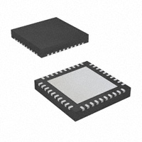


 工商网监
湘ICP备2023018690号
工商网监
湘ICP备2023018690号
