TPS65146
www.ti.com................................................................................................................................................... SLVS869A – NOVEMBER 2008 – REVISED JUNE 2009
Compact LCD Bias IC with LDO, VCOM Buffer and Reset Function
•
•
•
•
•
FEATURES
1
•
•
•
•
•
•
•
•
•
2.5V to 6.0V Input Voltage Range
Up to 16.5V Boost Converter With 2A Switch
Current
650kHz/1.2MHz Selectable Switching
Frequency
Adjustable Soft-Start for the Boost Converter
500mA LDO
Reset Function (XAO Signal)
Regulated VGH
Gate Voltage Shaping
VCOM Buffer
LCD Discharge Function
Overvoltage Protection
Thermal Shutdown
Undervoltage Lockout
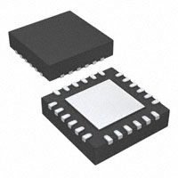
24-Pin 4×4mm QFN Package
APPLICATIONS
•
•
Notebook PC
Monitor
DESCRIPTION
The TPS65146 offers a very compact power supply solution designed to supply the LCD bias voltages required
by TFT (Thin Film Transistor) LCD panels running from a typical 3.3 V or 5 V supply rail. The device integrates a
step-up converter for VS (Source Driver voltage), a positive charge pump regulator for VGH (Gate Driver High
voltage), a logic voltage rail using an integrated LDO and a VCOM buffer driving the LCD backplane. In addition
to that, a gate voltage shaping block is integrated for VGH, modulating the signal (into VGHM) with high flexibility by
using a logic input VFLK and an external discharge resistor connected to RE pin. Also, an external discrete
negative charge pump can be set using the boost converter of the TPS65146 to generate VGL (Gate Driver Low
voltage). The integrated reset function together with the LCD discharge function available in the TPS65146
provide the signals enabling the discharge of the LCD TFT pixels when powering-off. The device includes safety
features like overvoltage protection (OVP), as well as thermal shutdown.
Space between text and graphic
Space between text and graphic
Space between text and graphic
VIN
3.3 V
Boost Converter
and
Over Voltage Protection
VS
9 V/300 mA
Positive Charge Pump Regulator,
Gate Voltage Shaping
and
LCD Discharge Function
VGHM
20 V/10 mA
LDO
VLVOUT
2.5 V/500 mA
VCOM Buffer
(unity gain)
VCOM
±120 mA
Reset function
XAO
1
Please be aware that an important notice concerning availability, standard warranty, and use in critical applications of Texas
Instruments semiconductor products and disclaimers thereto appears at the end of this data sheet.
PRODUCTION DATA information is current as of publication date.
Products conform to specifications per the terms of the Texas
Instruments standard warranty. Production processing does not
necessarily include testing of all parameters.
Copyright © 2008–2009, Texas Instruments Incorporated
�TPS65146
SLVS869A – NOVEMBER 2008 – REVISED JUNE 2009................................................................................................................................................... www.ti.com
These devices have limited built-in ESD protection. The leads should be shorted together or the device placed in conductive foam
during storage or handling to prevent electrostatic damage to the MOS gates.
ORDERING INFORMATION (1)
(1)
TA
ORDERING
PACKAGE
PACKAGE MARKING
–40°C to 85°C
TPS65146RGER
24-pin QFN
CEZ
The RGE package is available taped an reeled. For the most current package and ordering information, see the Package Option
Addendum at the end of this document, or see the TI website www.ti.com.
ABSOLUTE MAXIMUM RATINGS
over operating free-air temperature range (unless otherwise noted)
(1)
VALUE
UNIT
Input voltage range VIN, LVIN (2)
–0.3 to 6.5
V
Voltage range on pins FB, SS, FREQ, COMP, ADJ, LVOUT, XAO, FBP, VDPM, VFLK, VDET, CDET
–0.3 to 6.5
V
Voltage on pin SW, OPI, OPO, SUP, DRVP (2)
-0.3 to 20
V
(2)
Input voltage on VGH, VGHM, RE
(2)
-0.3 to 35
V
ESD rating HBM
2
kV
ESD rating MM
200
V
500
V
ESD rating CDM
Continuous power dissipation
See Dissipation
Rating Table
Storage temperature range
(1)
(2)
–65 to 150
°C
Stresses beyond those listed under absolute maximum ratings may cause permanent damage to the device. These are stress ratings
only, and functional operation of the device at these or any other conditions beyond those indicated under recommended operating
conditions is not implied. Exposure to absolute-maximum-rated conditions for extended periods may affect device reliability.
All voltage values are with respect to network ground terminal.
DISSIPATION RATINGS (1) (2)
(1)
(2)
PACKAGE
RθJA
TA ≤25°C
POWER RATING
TA = 70°C
POWER RATING
TA = 85°C
POWER RATING
QFN
30°C/W
3.3 W
1.8 W
1.3 W
PD = (TJ – TA)/RθJA.
RθJA. given for High-K PCB board.
RECOMMENDED OPERATING CONDITIONS (1) (2)
over operating free-air temperature range (unless otherwise noted)
MIN
VIN, VLVIN
Input voltage range, with VLVIN ≤ VIN
2.5
TA
Operating ambient temperature
TJ
Operating junction temperature
(1)
(2)
2
TYP
MAX
UNIT
6.0
V
–40
85
°C
–40
125
°C
Maximum output voltage limited by the Overvoltage Protection and not the maximum Power Switch rating.
Refer to application section for further information
Submit Documentation Feedback
Copyright © 2008–2009, Texas Instruments Incorporated
Product Folder Link(s) :TPS65146
�TPS65146
www.ti.com................................................................................................................................................... SLVS869A – NOVEMBER 2008 – REVISED JUNE 2009
ELECTRICAL CHARACTERISTICS
VIN = VLVIN = 3.3 V, VS = VSUP = 9 V, VLVOUT = 2.5 V, VGH = 20 V, TA = –40°C to 85°C, typical values are at TA = 25°C (unless
otherwise noted)
PARAMETER
TEST CONDITIONS
MIN
TYP
MAX
UNIT
SUPPLY
VIN
Input voltage range
IQIN
Operating quiescent current into VIN
Device not switching, VFB = 1.240 V + 3%
6.0
V
0.17
0.5
mA
IQLVIN
Operating quiescent current into LVIN
IQVGH
Operating quiescent current into VGH
VADJ = 1.240 V, VLVOUT = open, no load
25
45
µA
VFLK = GND
22
40
IQSUP
Operating quiescent current into SUP
Device not switching, VFB = 1.240 V + 3%
1.8
ISDVIN
Shutdown current into VIN
VIN = 1.8 V, VS = GND
20
33
µA
ISDVGH
Shutdown current into VGH
VIN = 1.8 V, VGH = 32 V
30
50
µA
ISDLVIN
Shutdown current into LVIN
VIN = 1.8 V, VLVOUT = open
0.1
2
µA
ISDSUP
Shutdown current into SUP
VIN = 1.8 V, VSUP = 16.5 V
3
5
µA
VUVLO
Under-voltage lockout threshold
TSD
Thermal shutdown
TSDHYS
Thermal shutdown hysteresis
2.5
VIN falling
2.0
2.2
VIN rising
2.3
Temperature rising
µA
mA
V
150
°C
14
°C
LOGIC SIGNALS FREQ, VFLK
ILEAK
Input leakage current
VFLK = 6.0 V, FREQ = GND
VIH
Logic high input voltage
VIN = 2.5 V to 6 V
VIL
Logic low input voltage
VIN = 2.5 V to 6 V
0.1
2
µA
V
0.5
V
BOOST CONVERTER
VS
Output voltage boost converter (1)
VOVP
Overvoltage protection
VS rising
VFB
Feedback regulation voltage
16.5
V
16.9
7
18
19
V
TA = -40°C to 85°C
1.226
1.240
1.254
V
TA = 25°C
1.230
1.240
1.250
IFB
Feedback input bias current
gm
Transconductiance error amplifier gain
VFB = 1.240V
RDS(ON)
N-channel MOSFET on-resistance
ILEAK_SW
SW leakage current
ILIM
N-Channel MOSFET current limit
ISS
Softstart current
fosc
Switching frequency
IFREQ
FREQ sink current
FREQ = 3.3 V
Line regulation
Load regulation
0.1
VIN = VGS = 5 V, ISW = current limit
0.13
0.38
VIN = VGS = 3.3 V, ISW = current limit
0.15
0.44
2.5
3.0
VIN = 1.8 V, VSW = 17 V
30
2.0
VSS = 1.240 V
µA
µA/V
115
Ω
µA
A
µA
4
FREQ = high
0.9
1.2
1.5
MHz
FREQ = low
470
625
780
kHZ
4
µA
VIN = 2.5 V to 6.0 V, IOUT = 10 mA
0.008
%/V
IOUT = 0 A to 500 mA, VIN = 3.3 V
0.15
%/A
LDO REGULATOR
VLVOUT
LDO output voltage range
VADJ
Feedback regulation voltage
IADJ
Feedback input bias current
VADJ = 1.240 V
0.1
µA
ISC_LDO
Short circuit current limit
VIN = VLVIN = 6 V, LVOUT = GND, ADJ = GND
750
mA
VDO
Dropout voltage
mV
(1)
4
V
ILVOUT = 2mA, VLVOUT = 1.240 V, TA = -40°C to
85°C
1.240
1.222
1.240
1.258
V
ILVOUT = 2mA, VLVOUT = 1.240 V, TA = 25°C
1.225
1.240
1.255
ILVOUT = 350 mA, VLVIN = VLVOUT – 0.1V
280
410
ILVOUT = 500 mA, VLVIN = VLVOUT – 0.1V
430
620
Line regulation
VLVIN = 2.7 V to 5.5 V, ILVOUT = 100 mA
0.005
%/V
Load regulation
ILVOUT = 1 mA to 300 mA
0.6
%/A
Maximum output voltage limited by the Overvoltage Protection and not the maximum power switch rating of the boost converter.
Submit Documentation Feedback
Copyright © 2008–2009, Texas Instruments Incorporated
Product Folder Link(s) :TPS65146
3
�TPS65146
SLVS869A – NOVEMBER 2008 – REVISED JUNE 2009................................................................................................................................................... www.ti.com
ELECTRICAL CHARACTERISTICS (continued)
VIN = VLVIN = 3.3 V, VS = VSUP = 9 V, VLVOUT = 2.5 V, VGH = 20 V, TA = –40°C to 85°C, typical values are at TA = 25°C (unless
otherwise noted)
PARAMETER
TEST CONDITIONS
MIN
TYP
MAX
UNIT
VGH REGULATOR
fSW
Switching frequency
VFBP
Reference voltage of feedback
0.5 × fOSC
MHz
IFBP
Feedback input bias current
VFBP= 1.240 V
0.1
µA
RDS(ON)Q1
DRVP RDS(ON) (Q1 PMOS)
VS = 9 V, IDRVP = 40 mA
8
20
Ω
RDS(ON)Q2
DRVP RDS(ON) (Q2 NMOS)
VS = 9 V, IDRVP = - 40 mA
2
6
Ω
TA = -40°C to 85°C
1.210
1.240
1.270
TA = 25°C
1.221
1.240
1.259
V
GATE VOLTAGE SHAPING VGHM
µA
IDPM
Capacitor charge current VDPM pin
RDS(ON)M1
VGH to VGHM RDS(ON) (M1 PMOS)
VFLK = low, IVGHM = 20 mA, VGH = 20 V
20
13
25
Ω
RDS(ON)M2
VGHM to RE RDS(ON) (M2 PMOS)
VFLK = high, IVGHM = 20 mA, VGHM = 7.5 V
13
25
Ω
6.0
V
RESET FUNCTION
VIN_DET
Operating voltage for VIN
1.6
Falling, TA = -40°C to 85°C
1.074
1.100
1.126
Falling, TA = 25°C
1.079
1.100
1.121
VDET
Threshold voltage
VDET_HYS
Threshold hysterisis
IDET_B
Iinput bias current
VDET = 1.1 V
ICDET
Delay capacitor charge current
VCDET ≤ 1.240 V
IXAO(ON)
Sink current capability (2)
VXAO(ON) = 0.5 V
VXAO(ON)
Low voltage level
IXAO(ON)= 1 mA
ILEAK_XAO
Leakage current
VXAO = VIN = 3.3V
V
65
mV
µA
0.1
µA
10
1
mA
0.5
V
2
µA
7
16.5
V
VCOM BUFFER
VSUP
VS supply range (3)
VOFFSET
Input offset voltage
VCM = VOPI = VSUP/2 = 4.5 V
–15
15
mV
IB
Input bias current
VCM = VOPI = VSUP/2 = 4.5 V
-1
1
µA
VCM
Common mode input voltage range
VOFFSET = 10 mV, IOPO = 10 mA
2
VS-2
CMRR
Common mode rejection ratio
VCM = VOPI = VSUP/2 = 4.5 V, 1 MHz
VOL
Output voltage swing low
IOPO = 10 mA
0.10
VOH
Output voltage swing high
IOPO = 10 mA
VS - 0.80 VS - 0.65
V
66
Source (VOPI = VSUP/2 = 4.5 V, OPO = GND)
90
135
100
160
dB
0.20
V
V
Isc
Short circuit current
Io
Output current
PSRR
Power supply rejection ratio
40
dB
SR
Slew rate
AV = 1, VOPI = 2 Vpp
40
V/µs
BW
–3db bandwidth
AV = 1, VOPI = 60 mVpp
60
MHz
(2)
(3)
4
Sink (VOPI = VSUP/2 = 4.5 V, VCOM = VSUP = 9 V)
Source (VOPI = VSUP/2 = 4.5V, VOFFSET = 15 mV)
120
Sink (VOPI = VSUP/2 = 4.5V, VOFFSET = 15 mV)
130
mA
mA
External pull-up resistor to be chosen so that the current flowing into XAO Pin (VXAO = 0 V) when active is below IXAO_MIN = 1mA.
Maximum output voltage limited by the Overvoltage Protection and not the maximum power switch rating of the boost converter.
Submit Documentation Feedback
Copyright © 2008–2009, Texas Instruments Incorporated
Product Folder Link(s) :TPS65146
�TPS65146
www.ti.com................................................................................................................................................... SLVS869A – NOVEMBER 2008 – REVISED JUNE 2009
PIN ASSIGNMENT
SW
1
VIN
2
PGND
FREQ
FB
COMP
OPI
OPO
24 Pin QFN Package 4x4 mm
(Top View)
24
23
22
21
20
19
PowerPAD
3
SS
18
SUP
17
DRVP
16
FBP
®
Exposed Thermal Die
5
14
VGHM
LVOUT
6
13
RE
8
9
10
11
12
VFLK
7
VDPM
ADJ
CDET
VGH
XAO
15
VDET
4
LVIN
AGND
TERMINAL FUNCTIONS
PIN
NAME
NO.
I/O
SW
1
VIN
2
I
SS
3
I/O
AGND
DESCRIPTION
Switch pin of the boost converter.
4, exposed
pad
Input supply pin.
Boost soft-start control pin. Connect a capacitor to this pin if a soft-start is needed. Open = no
soft-start.
Analog ground.
ADJ
5
I
LDO feedback pin.
LVOUT
6
O
LDO output pin.
LVIN
7
I
LDO input supply pin.
VDET
8
I
Reset function threshold pin. Connect a voltage divider to this pin to set the threshold voltage.
XAO
9
O
Reset function output pin (open-drain). XAO signal is active low.
CDET
10
I/O
Sets the reset delay time. Pin for external capacitor. Floating if no delay is needed.
VDPM
11
I/O
Sets the delay to enable VGHM Output. Pin for external capacitor. Floating if no delay needed.
VFLK
12
I
Input pin for charge/discharge signal for VGHM. VFLK = “high” discharges VGHM through RE pin.
RE
13
VGHM
14
O
Gate voltage shaping output pin
VGH
15
I
Input pin for the positive charge pump voltage.
FBP
16
I
Positive charge pump feedback pin.
DRVP
17
O
Voltage driver pin of the positive charge pump.
SUP
18
I
Input supply pin for the gate voltage shaping and operational amplifier blocks. Also overvoltage
protection sense pin. SUP pin must be supplied by VS voltage.
OPO
19
O
Output pin of the VCOM Buffer.
OPI
20
I
Input pin of the VCOM Buffer.
COMP
21
I/O
FB
22
I
Boost converter feedback pin.
FREQ
23
I
Boost converter frequency select pin. Oscillator is 650 kHz when FREQ is connected to GND and
1.2 MHz when FREQ is connected to VIN.
PGND
24
Slope adjustment pin for gate voltage shaping. Connect a resistor to this pin to set the discharging
slope of VGHM when VFLK = “high”.
Boost converter compensation pin .
Power ground.
Submit Documentation Feedback
Copyright © 2008–2009, Texas Instruments Incorporated
Product Folder Link(s) :TPS65146
5
�TPS65146
SLVS869A – NOVEMBER 2008 – REVISED JUNE 2009................................................................................................................................................... www.ti.com
FUNCTIONAL BLOCK DIAGRAM
VGL
VIN
SUP
SW
LVIN
FREQ
VIN
VS
FB
Boost Converter
(VS)
VLVOUT
LVOUT
LDO
(VLVOUT)
ADJ
DRVP
VLVOUT
Positive Charge
Pump Regulator
(VGH)
VIN
XAO
XAO
FBP
Reset Function
(XAO)
VDET
CDET
VGH
VS
VGHM
Gate Voltage
Shaping
(VGHM)
VGHM
RE
OPI
VCOM
OPO
VFLK
VCOM
(VCOM)
6
Submit Documentation Feedback
PGND
AGND
SS
COMP
VDPM
Copyright © 2008–2009, Texas Instruments Incorporated
Product Folder Link(s) :TPS65146
�TPS65146
www.ti.com................................................................................................................................................... SLVS869A – NOVEMBER 2008 – REVISED JUNE 2009
TYPICAL CHARACTERISTICS
TABLE OF GRAPHS
FIGURE
Efficieny vs Load Current
VIN = 3.3 V, VS = 9 V
f = 650 kHz/1.2 MHz
Figure 1
Efficiency vs Load Current
VIN = 3.3 V, VS = 12 V
f = 650 kHz/1.2 MHz
Figure 2
PWM Switching Discontinuous Conduction Mode
VIN = 3.3 V, VS = 9 V/ 4 mA
f = 1.2 MHz
Figure 3
PWM Switching Continuous Conduction Mode
VIN = 3.3 V, VS = 9 V/ 300 mA
f = 1.2 MHz
Figure 4
Boost Frequency vs Load Current
VIN = 3.3 V, VS = 9 V
f = 650 kHz/1.2 MHz
Figure 5
Boost Frequency vs Supply Voltage
VS = 9 V/150 mA, f = 650 kHz/1.2 MHz
Figure 6
Load Transient Response Boost Converter High
Frequency
VIN = 3.3 V, VS = 9 V
IOUT = 50 mA ~ 200 mA, f = 1.2 MHz
Figure 7
Load Transient Response Boost Converter Low
Frequency
VIN = 3.3 V, VS = 9 V
IOUT = 50 mA ~ 200 mA, f = 650 kHz
Figure 8
Soft-start Boost Converter
VIN = 3.3 V, VS = 9 V, IOUT = 300 mA
Figure 9
Overvoltage Protection Boost Converter (OVP)
VIN = 3.3 V, VS = 9 V
Figure 10
Load Transient Response LDO
VLVIN = 3.3 V, VLVOUT = 2.5 V
ILVOUT = 100 mA - 300 mA
Figure 11
Gate Voltage Shaping
VGH = 20 V
Figure 12
VGHM Voltage vs Load Current
VIN = 3.3 V, VS = 9 V, VGHM = 19.8 V
Figure 13
VGL Voltage vs Load Current
VIN = 3.3 V, VS = 9 V, VGL = -6.7 V
Figure 14
Power on Sequencing XAO Signal and VGHM
Delay
VIN = 3.3 V, VS = 9 V, VGHM = 20 V
Figure 15
Power off Sequencing XAO Signal and VGHM
Delay
VIN = 3.3 V, VS = 9 V, VGHM = 20 V
Figure 16
Power on Sequencing
VIN = 3.3 V, VS = 9 V, VLVOUT = 2.5 V,
VVCOM = 4.5V, VGHM = VGH = 20 V, VGL
= -7V
Figure 17
Power off Sequencing
VIN = 3.3 V, VS = 9 V, VLVOUT = 2.5 V,
VVCOM = 4.5V, VGHM = VGH = 20 V
VGL = -7V
Figure 18
For all the following graphics, the inductors used for the measurements are MSS7341 (L = 5 µF) for f = 1.2 MHz,
and CDRH8D28 (L = 10 µF) for f = 650 kHz.
EFFICIENCY
vs
LOAD CURRENT (Vs = 9 V)
EFFICIENCY
vs
Load Current (Vs = 12 V)
100
100
90
VIN = 3.3 V,
VS = 9 V
f = 650 kHz,
L = 10 mH
90
70
f = 1.2 MHz,
L = 5 mH
Efficiency - %
Efficiency - %
70
50
40
60
50
30
20
20
10
10
0.01
0.1
IO -Load current - A
1
f = 1.2 MHz,
L = 5 mH
40
30
0
0.001
f = 650 kHz,
L = 10 mH
80
80
60
VIN = 3.3 V,
VS = 12 V
0
0.001
Figure 1.
0.01
0.1
IO -Load current - A
1
Figure 2.
Submit Documentation Feedback
Copyright © 2008–2009, Texas Instruments Incorporated
Product Folder Link(s) :TPS65146
7
�TPS65146
SLVS869A – NOVEMBER 2008 – REVISED JUNE 2009................................................................................................................................................... www.ti.com
PWM SWITCHING
DISCONTINUOUS CONDUCTION MODE
PWM SWITCHING
CONTINUOUS CONDUCTION MODE
VSW
5 V/div
VSW
5 V/div
VS_AC
50 mV/div
VS_AC
50 mV/div
VIN = 3.3 V,
VS = 9 V/4 mA
IL
200 mA/div
VIN = 3.3 V,
VS = 9 V/300 mA
IL
200 mA/div
400 ns/div
400 ns/div
Figure 3.
Figure 4.
BOOST FREQUENCY
vs
LOAD CURRENT
BOOST FREQUENCY
vs
SUPPLY VOLTAGE
1600
1600
1400
VS = 9 V/150 mA
VIN = 3.3 V,
VS = 9 V
f = VIN
L = 5 mH
1200
f - Frequency - kHz
f - Frequency - kHz
1200
1000
f = GND
L = 10 mH
800
600
1000
600
400
200
200
0
0.1
0.4
0.2
0.3
IO - Load current - A
0.5
0.6
f = GND
L = 10 mH
800
400
0
0
2.0
2.5
3.0
3.5
4.0
4.5
VIN - Supply voltage - V
5.0
5.5
Figure 5.
Figure 6.
LOAD TRANSIENT RESPONSE
BOOST CONVERTER HIGH FREQUENCY
LOAD TRANSIENT RESPONSE
BOOST CONVERTER LOW FREQUENCY
VIN = 3.3 V,
VS = 9 V
VIN = 3.3 V,
VS = 9 V
COUT = 20 mF,
L = 5 mH,
RCOMP = 18 kW,
CCOMP = 3.3 nF
VS_AC
200 mV/div
6.0
COUT = 20 mF,
L = 10 mH,
RCOMP = 18 kW,
CCOMP = 3.3 nF
VS_AC
200 mV/div
IOUT
100 mA/div
IOUT
100 mA/div
IOUT = 50 mA - 200 mA
IOUT = 50 mA - 200 mA
200 ms/div
200 ms/div
Figure 7.
8
f = VIN
L = 5 mH
1400
Figure 8.
Submit Documentation Feedback
Copyright © 2008–2009, Texas Instruments Incorporated
Product Folder Link(s) :TPS65146
�TPS65146
www.ti.com................................................................................................................................................... SLVS869A – NOVEMBER 2008 – REVISED JUNE 2009
BOOST CONVERTER
SOFT-START
OVERVOLTAGE PROTECTION
BOOST CONVERTER (OVP)
VIN
VS
5 V/div
2 V/div
FB shorted
to GND
VIN = 5 V
VS = 15 V / 500 mA
VS
5 V/div
VSW
5 V/div
IL
CSS = 100 nF
500 mA/div
200 ms/div
10 ms/div
Figure 9.
Figure 10.
LOAD TRANSIENT RESPONSE LDO
GATE VOLTAGE SHAPING
VFLK
5 V/div
VLVOUT_AC
50 mV/div
VLVIN = 3.3 V
VLVOUT_AC
50 mV/div
VLVOUT = 2.5 V
COUT = 1 µF
VGHM
10 V/div
VGHM = 20 V down to GND
ILVOUT
200 mA/div
RE = 80 kW
ILVOUT = 100 mA - 300 mA
40 ms/div
10 µs/div
Figure 11.
Figure 12.
VGHM VOLTAGE
vs
LOAD CURRENT
VGL VOLTAGE
vs
LOAD CURRENT
20.5
0
20.0
VIN = 3.3 V
-1
TA = - 40 °C
VS = 9 V
-3
VGL - V
19.0
VGHM - V
VGH = -6.7 V
-2
TA = 25 °C
19.5
18.5
VIN = 3.3 V
18.0
-4
TA = - 40 °C
-5
TA = 25 °C
VS = 12 V
TA = 85 °C
VGH = 19.8 V
17.5
-6
17.0
-7
16.5
-8
TA = 85 °C
0
10
20
30
40
50
60
70
80
90
100
0
10
20
30
40
50
60
70
lGL - Load Current - mA
IGH - Load Current - mA
Figure 13.
Figure 14.
Submit Documentation Feedback
Copyright © 2008–2009, Texas Instruments Incorporated
Product Folder Link(s) :TPS65146
9
�TPS65146
SLVS869A – NOVEMBER 2008 – REVISED JUNE 2009................................................................................................................................................... www.ti.com
POWER ON SEQUENCING
XAO SIGNAL AND VGHM DELAY
VIN
2 V/div
Set by
CDET
POWER OFF SEQUENCING
XAO SIGNAL AND VGHM DELAY
VIN
2 V/div
VDET_threshold
reached
XAO
2 V/div
XAO
2 V/div
VFLK
5 V/div
VFLX
5 V/div
VGHM
10 V/div
Set by
CDPM
VGHM
10 V/div
VGHM = VGH
Boost PG
10 ms/div
10 ms/div
Figure 15.
Figure 16.
POWER ON SEQUENCE
VIN
5 V/div
POWER OFF SEQUENCE
VIN
5 V/div
VLVOUT
5 V/div
VS
10 V/div
VLVOUT
5 V/div
VS
10 V/div
VCOM
10 V/div
VGH
VGHM
VCOM
10 V/div
10 V/div
VGH
VGHM
10 V/div
VGL
10 V/div
10
VGL
10 V/div
10 ms/div
10 ms/div
Figure 17.
Figure 18.
Submit Documentation Feedback
Copyright © 2008–2009, Texas Instruments Incorporated
Product Folder Link(s) :TPS65146
�TPS65146
www.ti.com................................................................................................................................................... SLVS869A – NOVEMBER 2008 – REVISED JUNE 2009
APPLICATION INFORMATION
BOOST CONVERTER
VIN
VS
VIN
SW
FREQ
p
p
SUP
Over Voltage
Protection
(OVP)
SS
Current limit
and
Soft Start
Toff Generator
Bias Vref = 1 .24 V
UVLO
Thermal Shutdown
Ton
PWM
Generator
Gate Driver of
Power
Transistor
COMP
GM Amplifier
FB
Vref
PGND
p
Figure 19. Boost converter block diagram
The boost converter is designed for output voltages up to 16.5 V with a switch peak current limit of 2.0 A
minimum. The device, which operates in a current mode scheme with quasi-constant frequency, is externally
compensated for maximum flexibility and stability. The switching frequency is selectable between 650 kHz and
1.2 MHz and the minimum input voltage is 2.5 V. To limit the inrush current at start-up a soft-start pin is
available.
During the on-time, the current rises into the inductor. When the current reaches a threshold value set by the
internal GM amplifier, the power transistor is turned off. The polarity of the inductor changes and forward biases
the Schottky diode which lets the current flow towards the output of the boost converter. The off-time is fixed for
a certain VIN and VS, and therefore maintains the same frequency when varying these parameters.
However, for different output loads, the frequency slightly changes due to the voltage drop across the RDS(ON) of
the power transistor which will have an effect on the voltage across the inductor and thus on tON (tOFF remains
fixed).
The fixed off-time maintains a quasi-fixed frequency that provides better stability for the system over a wide
range of input and output voltages than conventional boost converters. The TPS65146 topology has also the
benefits of providing very good load and line regulations, and excellent line and load transient responses.
Submit Documentation Feedback
Copyright © 2008–2009, Texas Instruments Incorporated
Product Folder Link(s) :TPS65146
11
�TPS65146
SLVS869A – NOVEMBER 2008 – REVISED JUNE 2009................................................................................................................................................... www.ti.com
Boost Converter Design Procedure
The first step in the design procedure is to verify whether the maximum possible output current of the boost
converter supports the specific application requirements. A simple approach is to estimate the converter
efficiency, by taking the efficiency numbers from the provided efficiency curves or to use a worst case
assumption for the expected efficiency, e.g. 85%.
1. Duty Cycle:
D=
VIN ´h
VS
2. Inductor ripple current:
ΔIL =
3. Maximum output current:
4. Peak switch Current:
VIN ´ D
f ´L
ΔIL ö
æ
´ (1 - D)
IOUT_max = ç ILIM_min 2 ÷ø
è
Iswpeak =
I
ΔIL
+ out
2
1- D
Iswpeak = converter switch current (must be < ILIM_min = 2.0 A)
ƒS = Converter switching frequency (typically 1.2 MHz or 650 kHz)
L = Selected inductor value (see the Inductor Selection section)
η = Estimated converter efficiency (please use the number from the efficiency plots or 85% as an estimation)
ΔIL = Inductor peak-to-peak ripple current
The peak switch current is the steady state peak switch current the integrated switch, inductor and external
Schottky diode has to be able to handle. The calculation must be done for the minimum input voltage where the
peak switch current is highest.
Soft-Start (Boost Converter)
The boost converter has an adjustable soft-start to prevent high inrush current during start-up. To minimize the
inrush current during start-up an external capacitor connected to the soft-start pin SS is used to slowly ramp up
the internal current limit of the boost converter. When the VIN exceeds the Undervoltage Lockout (UVLO)
threshold, the soft-start capacitor CSS is immediately charged up to 0.3 V. The capacitor is then charged at a
constant current of 4 µA typically until the output of the boost converter VS has reached its Power Good threshold
(90% of VS nominal value). During this time, the voltage on SS pin directly controls the peak inductor current,
starting with 0 A at VSS = 0.3 V up to the full current limit at VSS ≈ 800 mV. The maximum load current is
available after the soft-start is completed. The larger the capacitor, the slower the ramp of the current limit and
the longer the soft-start time. A 100 nF capacitor is usually sufficient for most of the applications. When VIN falls
down below the UVLO level, the soft-start capacitor is discharged to ground.
Frequency Select Pin (FREQ)
The digital frequency select pin FREQ allows to set the switching frequency of the device to 650 kHz (FREQ =
low) or 1.2 MHz (FREQ = high). Higher switching frequency improves load transient response but reduces
slightly the efficiency. The other benefits of higher switching frequency are a lower output voltage ripple. Usually,
it is recommended to use 1.2 MHz switching frequency unless light load efficiency is a major concern.
Inductor Selection
The main parameter for the inductor selection is the saturation current of the inductor which should be higher
than the peak switch current as calculated above with additional margin to cover for heavy load transients. An
alternative, more conservative, is to choose the inductor with a saturation current at least as high as the
maximum switch current limit of 3.0 A. Another important parameter is the inductor DC resistance. Usually the
lower the DC resistance the higher the efficiency. It is important to note that the inductor DC resistance is not the
only parameter determining the efficiency. Especially for a boost converter where the inductor is the energy
storage element, the type and core material of the inductor influences the efficiency as well. At high switching
12
Submit Documentation Feedback
Copyright © 2008–2009, Texas Instruments Incorporated
Product Folder Link(s) :TPS65146
�TPS65146
www.ti.com................................................................................................................................................... SLVS869A – NOVEMBER 2008 – REVISED JUNE 2009
frequencies of 1.2 MHz inductor core losses, proximity effects and skin effects become more important. Usually
an inductor with a larger form factor gives higher efficiency. The efficiency difference between different inductors
can vary between 2% to 10%. For the TPS65146, inductor values between 3.3 µH and 6.8 µH are a good choice
with a switching frequency of 1.2 MHz. At 650 kHz we recommend inductors between 7 µH and 13 µH. Isat ≥
Iswpeak imperatively. Possible inductors are shown in Table 1.
Table 1. Inductor Selection
L
(µH)
COMPONENT SUPPLIER
COMPONENT CODE
SIZE
(LxWxH mm)
DCR TYP
(mΩ)
Isat
(A)
4.7
Sumida
CDRH3D14
4.7
4 × 4 × 1.5
120
1.1
Coilcraft
LPS4414-472ML
4.3 × 4.3 × 1.4
215
1.5
4.2
Sumida
CDRH5D28
5.7 × 5.7 × 3
23
2.2
5.0
Coilcraft
MSS7341
7.3 × 7.3 × 4.1
24
2.9
1.2 MHz
650 kHz
10
Sumida
CDC5D23B
6 × 6 × 2.5
102
1.04
10
Sumida
CDR6D23MNNP
5 × 5 × 2.4
83
1.75
10
Würth Elektronik
744778910
7.3 × 7.3 × 3.2
51
2.2
10
Sumida
CDRH8D28
8.3 × 8.3 × 3
36
2.5
Rectifier Diode Selection
To achieve high efficiency a Schottky type should be used for the rectifier diode. The reverse voltage rating
should be higher than the maximum output voltage of the converter. The averaged rectified forward current Iavg,
the Schottky diode needs to be rated for, is equal to the output current IOUT:
IF = IOUT
(1)
Usually a Schottky diode with 1 A to 1.5 A maximum average rectified forward current rating is sufficient for most
of the applications. Also, the Schottky rectifier has to be able to dissipate the power. The dissipated power is the
average rectified forward current IF times the diode forward voltage VF (or VDiode).
PD = IF × VF
Typically the diode should be able to dissipate around 500mW depending on the load current and forward
voltage.
Table 2. Rectifier Diode Selection
CURRENT
RATING lF
VR
VF / IF
COMPONENT SUPPLIER
COMPONENT CODE
PACKAGE TYPE
750 mA
20 V
0.425 V/750 mA
Fairchild Semiconductor
FYV0704S
SOT 23
1A
20 V
0.39 V/1 A
NXP
PMEG2010AEH
SOD 123
1A
20 V
0.5 V/1 A
Vishay
SS12
SMA
1A
20 V
0.44 V/1 A
Vishay
MSS1P2L
µ-SMP (Low Profile)
1.5 A
25 V
0.5 V/1 A
Vishay
BYS10-25
SMA
Submit Documentation Feedback
Copyright © 2008–2009, Texas Instruments Incorporated
Product Folder Link(s) :TPS65146
13
�TPS65146
SLVS869A – NOVEMBER 2008 – REVISED JUNE 2009................................................................................................................................................... www.ti.com
Setting the Output Voltage
The output voltage is set by an external resistor divider. Typically, a minimum current of 50 µA flowing through
the feedback divider is enough to cover the noise fluctuation. The resistors are then calculated with 70 µA as:
VS
R2 =
æ V
ö
R1 = R2 ´ ç S - 1÷
è VFB
ø
VFB
» 18 kΩ
70 μA
R1
VFB
R2
(2)
with VFB = 1.240 V
Compensation (COMP)
The regulation loop can be compensated by adjusting the external components connected to the COMP pin. The
COMP pin is the output of the internal transconductance error amplifier. The compensation capacitor will adjust
the low frequency gain and the resistor value will adjust the high frequency gain. Lower output voltages require a
higher gain and therefore a lower compensation capacitor value. A good start, that will work for the majority of
the applications is CCOMP = 3.3 nF and RCOMP = 18 kΩ for a 3.3 V input.
Input Capacitor Selection
For good input voltage filtering low ESR ceramic capacitors are recommended. TPS65146 has an analog input
VIN. A 1-µF bypass is required as close as possible from VIN to GND.
One 10-µF ceramic input capacitor is sufficient for most of the applications. For better input voltage filtering this
value can be increased. Refer to Table 3 and typical applications for input capacitor recommendations.
Output Capacitor Selection
For best output voltage filtering a low ESR output capacitor is recommended. Two 10-µF ceramic output
capacitors work for most of the applications. Higher capacitor values can be used to improve the load transient
response. Refer to Table 3 for the selection of the output capacitor.
Table 3. Rectifier Input and Output Capacitor Selection
CAPACITOR
VOLTAGE
RATING
COMPONENT SUPPLIER
COMPONENT CODE
COMMENTS
10 µF/0805
10 V
Taiyo Yuden
LMK212 BJ 106KD
CIN
1 µF/0603
10 V
Taiyo Yuden
EMK107 BJ 105KA
VIN bypass
10 µF/1206
25 V
Taiyo Yuden
TMK316 BJ 106ML
COUT
To calculate the output voltage ripple that following equations can be used:
V - VIN IOUT
DVC = S
´
DVC_ESR = DIL ´ RC_ESR
VS ´ f
C
(3)
ΔVC_ESR can be neglected in many cases since ceramic capacitors provide very low ESR.
14
Submit Documentation Feedback
Copyright © 2008–2009, Texas Instruments Incorporated
Product Folder Link(s) :TPS65146
�TPS65146
www.ti.com................................................................................................................................................... SLVS869A – NOVEMBER 2008 – REVISED JUNE 2009
Undervoltage Lockout (UVLO)
To avoid mis-operation of the device at low input voltages an undervoltage lockout is included that disables the
device, if the input voltage falls below 2.0 V.
Thermal shutdown
A thermal shutdown is implemented to prevent damages because of excessive heat and power dissipation.
Typically the thermal shutdown threshold for the junction temperature is 150°C. When the thermal shutdown is
triggered the device stops switching until the junction temperature falls below typically 136 °C. Then the device
starts switching again.
Overvoltage Protection
The boost converter has an integrated overvoltage protection to prevent the power switch from exceeding the
absolute maximum switch voltage rating at pin SW in case the feedback (FB) pin is floating or shorted to GND. In
such an event, the output voltage rises and is monitored with the overvoltage protection comparator over the
SUP pin. As soon as the comparator trips at typically 18 V, the boost converter turns the N-Channel MOSFET
switch off. The output voltage falls below the overvoltage threshold and the converter continues to operate. In
order to detect overvoltage, the SUP pin needs to be connected to the output voltage of the boost converter VS.
LOW DROPOUT LINEAR REGULATOR (LDO)
The TPS65146 includes a Low Dropout Regulator providing the logic voltage to the panel. The LDO is designed
to operate typically with a 1-µF ceramic output capacitor. The LDO has an internal softstart feature to limit the
inrush current. A minimum current of 50 µA flowing through the feedback divider is usually enough to cover the
noise fluctuation. The resistors of the voltage divider are then calculated with 70 µA as:
VLVOUT
R4 =
VADJ
» 18 kW
70 μA
æV
ö
R3 = R4 ´ ç LVOUT - 1÷
è VADJ
ø
R3
VADJ
R4
(4)
with VADJ = 1.240 V
Submit Documentation Feedback
Copyright © 2008–2009, Texas Instruments Incorporated
Product Folder Link(s) :TPS65146
15
�TPS65146
SLVS869A – NOVEMBER 2008 – REVISED JUNE 2009................................................................................................................................................... www.ti.com
REGULATED POSITIVE CHARGE PUMP
The positive charge pump sets the voltage applied on the VGH input pin, up to 32 V in tripler mode configuration.
The charge pump block regulates the VGH voltage by adjusting the drive current IDRVP. Typically, a minimum
current of 50 µA flowing through the feedback divider is usually enough to cover the noise fluctuation. The
resistors of the divider used to set the VGH voltage are calculated as:
VGH
R11 =
æ V
ö
R10 = R11 ´ ç GH - 1÷
è VFBP
ø
VFBP
» 18 kW
70 μA
R10
VFBP
R11
(5)
with VFBP = 1.240 V
2 VS
3 VS
VS
VIN
SW
SUP
DRVP
Power
Transistor Boost
VGH
ISOURCE (Q1)
Clock Boost
Converter
2
Positive
Charge
Pump
Regulator
ISINK (Q2)
M1
Gate Voltage
Shaping
(GPM)
VFLK
M2
VGHM
RE
VDPM
FBP
Vref
AGND
PGND
Figure 20. Positive Charge Pump regulator and Gate Voltage Shaping blocks
Doubler Mode: to use the positive Charge Pump in doubler mode configuration, the Schottky diode connected
between the capacitor of DRVP pin and the 2.VS point has to be connected to the 3.VS point (seeFigure 20).
Tripler Mode: since VGH pin is rated to maximum 32 V, the maximum output voltage of the boost converter (VS)
possible is then limited to 11 V.
16
Submit Documentation Feedback
Copyright © 2008–2009, Texas Instruments Incorporated
Product Folder Link(s) :TPS65146
�TPS65146
www.ti.com................................................................................................................................................... SLVS869A – NOVEMBER 2008 – REVISED JUNE 2009
POSTIVE CHARGE PUMP CURRENT CAPABILITY
The possible output current that the positive charge pump is able to deliver in doubler mode depends mainly on
the headroom (2*VS - VGH) and the internal voltage drop Vdrop_internal. The graph below (Figure 21) helps defining
the headroom range that the system needs:
Positive Charge Pump Output Current
vs Internal Vdrop
70
65
Maximum IGH possible
60
55
PDISS_INTERNAL = 200 mW
50
PDISS_INTERNAL = 150 mW
Igh - mA
45
PDISS_INTERNAL = 100 mW
40
35
PDISS_INTERNAL = 50 mW
30
25
20
15
10
5
0
0
1
2
3
4
5
6
7
8
9
10
Vdrop_internal for Positive Charge Pum p - V
Figure 21.
Example:
For IGH = 20 mA, we refer to the “maximum IGH possible” curve to determine the minimum headroom needed.
Vheadroom _ 20mA = 2.VSUP - VGH ³ Vdrop _ int_ 20mA + 2.VDiode * = 0.5 + 2 V = 2.5V
(6)
* in the case where VDiode = 1 V
This means that the headroom in this example must be more than 2.5 V to be able to source 20 mA at the output
of the positive charge pump.
However, generating a too large headroom can lead to excessive power dissipation. The dashed curves show
the internal power dissipation generated by a certain internal voltage drop. In the above example, if Vheadroom_20mA
= 7 V (with VDiode = 1 V), Vdrop_internal_min = 5 V and the internal power dissipation PDISS_INTERNAL for the positive
charge pump would reach 100 mW. The power dissipation of the charge pump block needs to be taken into
account for the overall power dissipation rating.
NOTE:
refer to the power rating table not to exceed the overall maximum package power
dissipation allowed.
Submit Documentation Feedback
Copyright © 2008–2009, Texas Instruments Incorporated
Product Folder Link(s) :TPS65146
17
�TPS65146
SLVS869A – NOVEMBER 2008 – REVISED JUNE 2009................................................................................................................................................... www.ti.com
EXTERNAL NEGATIVE CHARGE PUMP
The external negative charge pump works with two stages (charge pump and regulation). The charge pump
provides a negative regulated output voltage. Figure 22 shows the operation details of the negative charge
pump. With the first stage, the voltage on the collector of the bipolar transistor is equal to –VS+VD.
The next stage regulates the output voltage VGL. A resistor and a Zener diode are used to clamp the voltage to
the desired output value. The bipolar transistor is used to provide better load regulation as well as to reduce the
quiescent current. The output voltage on VGL will be equal to –VZ–Vbe.
VGL
-7 V/10 mA
T1
BC857B
C22
1 mF/
16 V
D2
BAV99
-VS
R14
6.8 kW
C14
470 nF
C13
470 nF
D8
BZX84C
7V5
D3
BAV99
VIN
2.5 V to 6 V
D1
Q1
VS
9 V/300 mA
Figure 22. Partially Regulated External Negative
Capacitors (Charge Pumps)
For best output voltage filtering a low ESR output capacitor is recommended. Ceramic capacitors have a low
ESR value but depending on the application tantalum capacitors can be used as well. For every capacitor, the
reactance value has to be calculated as follows:
1
Xc =
2 ´ p ´ f ´ C
(7)
This value should be as low as possible in order to reduce the voltage drop due to the current flowing through it.
The rated voltage of the capacitor has to be able to withstand the voltage across it. Capacitors rated at 50 V are
enough for most of the applications. Typically a 470-nF capacitance is sufficient for the flying capacitors whereas
bigger values like 1 µF or more can be used for the output capacitors to reduce the output voltage ripple.
CAPACITOR
COMPONENT SUPPLIER
COMPONENT CODE
COMMENTS
100 nF/0603
Taiyo Yuden
UMK107 BJ 104KA
Flying Cap
470 nF/0805
Taiyo Yuden
UMK212 BJ 474KG
Output Cap 1
1 µF/1210
Taiyo Yuden
UMK325 BJ 105KH
Output Cap 2
Diodes (Charge Pumps)
For high efficiency, one has to minimize the forward voltage drop of the diodes. Schottky diodes are
recommended. The reverse voltage rating must withstand the maximum output voltage VS of the boost converter.
Usually a Schottky diode with 200 mA average forward rectified current is suitable for most of the applications.
CURRENT
RATING Iavg
Vr
Vforward / Iavg
COMPONENT
SUPPLIER
COMPONENT
CODE
PACKAGE
TYPE
200 mA
30 V
0.5V / 30mA
International Rectifier
BAT54S
SOT 23
GATE VOLTAGE SHAPING FUNCTION
Sequencing
At start-up, the VGHM output is enabled once VDPM voltage is higher than Vref = 1.240 V. The capacitor
connected to VDPM pin sets a delay from the Power Good signal of the boost converter.
18
Submit Documentation Feedback
Copyright © 2008–2009, Texas Instruments Incorporated
Product Folder Link(s) :TPS65146
�TPS65146
www.ti.com................................................................................................................................................... SLVS869A – NOVEMBER 2008 – REVISED JUNE 2009
CVDPM =
IDPM ´ tDPM
20 m A ´ tDPM
=
Vref
1.240 V
(8)
At power off, VGHM is connected to VGH as soon as VIN reaches the threshold voltage of the reset function.
Setting the Discharge Slope for Gate Voltage Shaping
VFLK = ‘high’ → VGHM discharges to 0V
VFLK = ‘low’ → VGHM = VGH
The slope at which VGHM discharges is set by the external resistor connected to RE, the internal MOSFET
RDS(ON) (typ. 13Ω for M2 – see block diagram below) and by the external gate line capacitance connected to
VGHM pin.
Boost
Power Good
VFLK
VFLK = “high”
VFLK = “low”
Unknown state
Delay set
by VDPM
VGH
Slope set
by RE
VGHM
0V
Figure 23. Gate Voltage Shaping Timing
If VFLK = ’high’ and RE is connected with a resistor to ground (see Figure 23), VGHM will discharge from VGH to
0V. Since 5*τ ( τ = R*C) are needed to fully discharge C through R, we can define the time-constant of the gate
voltage shaping block as follow:
τ = (Re + RDS(ON)M2) × CVGHM
Therefore, if the discharge of CVGHM should finish during VFLK = 'high':
t VFLK = 'high'
Þ
- RDS(ON)M2
t discharge = 5 ´ t = t VFLK = 'high'
RE =
5 ´ CVGHM
(9)
VS
VS
VGHM
Re
M2
RE
Re’
Option 2
Option 3
Option 1
Re
Re
Figure 24. Discharge Path Options for VGHM
Options 2 and 3 from Figure 24 work like option 1 explained above. When M2 is turned on, VGHM discharges with
a slope set by Re from VGH level down to VS in option 2 configuration and in option 3 configuration down to the
voltage set by the resistor divider. The discharging slope is set by Re resistor(s).
NOTE:
when options 2 or 3 are used, VGHM is not held to 0V at startup but to the voltage set
on RE pin by the resistors Re and Re’.
Submit Documentation Feedback
Copyright © 2008–2009, Texas Instruments Incorporated
Product Folder Link(s) :TPS65146
19
�TPS65146
SLVS869A – NOVEMBER 2008 – REVISED JUNE 2009................................................................................................................................................... www.ti.com
VCOM BUFFER
The VCOM Buffer power supply pin is the SUP pin connected to the boost converter VS. To achieve good
performance and minimize the output noise, a 1-µF ceramic bypass capacitor is required directly from the SUP
pin to ground. The buffer is not designed to drive high capacitive loads; therefore it is recommended to connect a
series resistor at the output to provide stable operation when driving high capacitive load. With a 3.3-Ω series
resistor, a capacitive load of 10 nF can be driven, which is usually sufficient for typical LCD applications.
RESET FUNCTION
The device has an integrated reset function with an open drain output capable of sinking 1 mA. The reset
function monitors the voltage applied to its sense input VDET. As soon as the voltage on VDET falls below the
threshold voltage (VDET) of typically 1.1 V, the reset function asserts its reset signal by pulling XAO low. Typically,
a minimum current of 50µA flowing through the feedback divider is enough to cover the noise fluctuation.
Therefore, to select R6, one has to set the input voltage limit (VIN_LIM) at which the reset function will pull XAO to
low state. VIN_LIM must be higher than the UVLO threshold.
VIN
R7 =
æ VIN_LIM
ö
R6 = R7 ´ ç
- 1÷
è 1.1 V
ø
VDET
» 18 kW
70 μA
R6
VDET
R7
(10)
with VDET = 1.1 V
When the input voltage VIN rises, once the voltage on VDET pin exceeds its threshold voltage plus hysterisis the
XAO signal will go high after the delay time set by the capacitor connected to CDET.
10 m A ´ tDET
CDET =
1.240 V
(11)
The reset function is operational for VIN ≥ 1.6 V.
VDET
VDET_threshold_hys
VDET_threshold
Min. Operating
voltage
1.6 V
GND
XAO
Unknown
state
Delay set by
CDET
GND
Figure 25. Voltage Detection and XAO Pin
The reset function is configured as a standard open-drain and requires a pull-up resistor. The resistor RXAO (R5)
which must be connected between the XAO pin and a positive voltage VX greater than 2V - 'high' logic level - e.g.
VLVOUT , can be chosen as follows:
V
V - 2V
R XAO_min > X
&
R XAO_max < X
1 mA
2 mA
(12)
20
Submit Documentation Feedback
Copyright © 2008–2009, Texas Instruments Incorporated
Product Folder Link(s) :TPS65146
�TPS65146
www.ti.com................................................................................................................................................... SLVS869A – NOVEMBER 2008 – REVISED JUNE 2009
Power on sequencing
Once the input voltage VIN reaches the Under Voltage Lockout (UVLO), the device is internally enabled and the
LDO starts rising. When VLVOUT of the LDO is at its Power Good voltage, the boost converter, as well as the
Vcom buffer are enabled. As soon as VS of the boost converter reaches its Power Good (90% of its nominal
value), the positive charge pump block is enabled. Then the capacitor connected to VDPM is charged, setting the
gate voltage shaping block delay time, and finally enables the VGHM signal.
1. LDO
2. Boost converter & VCOM Buffer
3. VGH and VDPM (delay time to enable the gate voltage shaping function)
4. VGHM (after proper delay)
UVLO
VIN
VDET_THRESHOLD
UVLO
Device
ENABLED
Device
DISABLED
LDO
BOOST
VCOM
VGH
VGL (external)
VDPM
Vref
VFLK
Unknown state
Unknown state
Delay set
by VDPM
Slope set
by RE
VGHM
Co
n
to nec
VG te
H d
Di = L
s C
Fu ch D
nc arg
tio e
n
Figure 26. Sequencing TPS65146
Power off sequencing and LCD discharge function
When the input voltage VIN falls below a predefined threshold (set by VDET_THRESHOLD - see Figure 26 ), XAO is
driven low and VGHM is driven to VGH. (Note that when VIN falls below the UVLO threshold, all IC functions are
disabled except XAO and VGHM). Since VGHM is connected to VGH, it tracks the output of the positive charge
pump as it decays. This feature, together with XAO can be used to discharge the panel by turning on all the pixel
TFTs and discharging them into the gradually decaying VGHM voltage. VGHM is held low during power-up.
Submit Documentation Feedback
Copyright © 2008–2009, Texas Instruments Incorporated
Product Folder Link(s) :TPS65146
21
�TPS65146
SLVS869A – NOVEMBER 2008 – REVISED JUNE 2009................................................................................................................................................... www.ti.com
APPLICATION INFORMATION
C14
470 nF
T1
BC857B
C13
470 nF
R14
6.8 kW
C12
1 µF/
16 V
p
D8
BZX84C
7V5
p
D2
BAT54S
p
L
10 µH
VIN
3.3 V
FREQ
p
C4
10 µF/
25 V
C3
1 µF/
10 V
LVOUT
R3
18 kW
C9
1 µF/
6.3 V
R5
10 kW
p
p
C6
1 µF/
25 V
R1
200 kW
FB
R2
18 kW
LDO
(VLVOUT)
ADJ
DRVP
VLVOUT
R6
27 kW
p
C5
10 µF/
25 V
R4
18 kW
p
C18
470 nF
VS
15 V/200 mA
Boost Converter
(VS)
VLVOUT
2.5 V/300 mA
VIN
p
SW
p
p
D3
BAT54S
D1
PMEG2010AEH
LVIN
C2
1 µF/
10 V
VIN
C1
10 µF/
10 V
C16
1 µF/
50V
SUP
VGL
-7 V/10 mA
Positive Charge
Pump Regulator
(VGH)
XAO
XAO
FBP
Reset Function
(XAO)
VDET
R10
330 kW
R11
18 kW
R7
18 kW
CDET
VGH
C10
100 nF
VS
R8
18 kW
R9
18 kW
VGHM
Gate Voltage
Shaping
(VGHM)
RE
OPI
VCOM
4.5 V/100 mA
OPO
VFLK
VCOM
(VCOM)
VGHM
24 V/10 mA
R12
80 kW
p
R13
18 kW
C7
3.3 nF
C8
100 nF
PGND
AGND
SS
COMP
VDPM
C11
100 nF
p
Figure 27. TPS65146 Typical Application with Positive Charge Pump in Doubler Mode Configuration
22
Submit Documentation Feedback
Copyright © 2008–2009, Texas Instruments Incorporated
Product Folder Link(s) :TPS65146
�TPS65146
www.ti.com................................................................................................................................................... SLVS869A – NOVEMBER 2008 – REVISED JUNE 2009
C14
470 nF
T1
BC857B
C13
470 nF
R14
6.8 kW
C12
1 µF/
16 V
p
D8
BZX84C
7V5
p
p
L
10 µH
LVOUT
R3
18 kW
C9
1 µF/
6.3 V
p
R1
113 kW
R2
18 kW
LDO
(VLVOUT)
ADJ
DRVP
VLVOUT
R5
10 kW
p
C6
1 µF/
25 V
FB
R4
18 kW
p
R6
27 kW
p
C5
10 µF/
25 V
Boost Converter
(VS)
VLVOUT
2.5 V/300 mA
VIN
VS
9 V/300 mA
SW
FREQ
p
p
LVIN
p
C4
10 µF/
25 V
p
D3
BAT54S
D1
PMEG2010AEH
C3
1 µF/
10 V
C17
1 µF/
50 V
C18
470 nF
C16
470 nF
p
VIN
C2
1 µF/
10 V
D4
BAT54S
D2
BAT54S
VIN
2.5 V to 6 V
C1
10 µF/
10 V
C15
470 nF
SUP
VGL
-7 V/10 mA
Positive Charge
Pump Regulator
(VGH)
XAO
XAO
FBP
Reset Function
(XAO)
VDET
R10
270 kW
R11
18 kW
R7
18 kW
CDET
VGH
C10
100 nF
VS
R8
18 kW
R9
18 kW
VGHM
Gate Voltage
Shaping
(VGHM)
RE
OPI
VCOM
4.5 V/100 mA
OPO
VFLK
VCOM
(VCOM)
VGHM
20 V/10 mA
R12
80 kW
p
R13
18 kW
C7
3.3 nF
C8
100 nF
C11
100 nF
PGND
AGND
SS
COMP
VDPM
p
Figure 28. TPS65146 Typical Application with Positive Charge Pump in Tripler Mode Configuration
Submit Documentation Feedback
Copyright © 2008–2009, Texas Instruments Incorporated
Product Folder Link(s) :TPS65146
23
�PACKAGE OPTION ADDENDUM
www.ti.com
10-Dec-2020
PACKAGING INFORMATION
Orderable Device
Status
(1)
Package Type Package Pins Package
Drawing
Qty
Eco Plan
(2)
Lead finish/
Ball material
MSL Peak Temp
Op Temp (°C)
Device Marking
(3)
(4/5)
(6)
TPS65146RGER
ACTIVE
VQFN
RGE
24
3000
RoHS & Green
NIPDAU
Level-2-260C-1 YEAR
-40 to 85
CEZ
(1)
The marketing status values are defined as follows:
ACTIVE: Product device recommended for new designs.
LIFEBUY: TI has announced that the device will be discontinued, and a lifetime-buy period is in effect.
NRND: Not recommended for new designs. Device is in production to support existing customers, but TI does not recommend using this part in a new design.
PREVIEW: Device has been announced but is not in production. Samples may or may not be available.
OBSOLETE: TI has discontinued the production of the device.
(2)
RoHS: TI defines "RoHS" to mean semiconductor products that are compliant with the current EU RoHS requirements for all 10 RoHS substances, including the requirement that RoHS substance
do not exceed 0.1% by weight in homogeneous materials. Where designed to be soldered at high temperatures, "RoHS" products are suitable for use in specified lead-free processes. TI may
reference these types of products as "Pb-Free".
RoHS Exempt: TI defines "RoHS Exempt" to mean products that contain lead but are compliant with EU RoHS pursuant to a specific EU RoHS exemption.
Green: TI defines "Green" to mean the content of Chlorine (Cl) and Bromine (Br) based flame retardants meet JS709B low halogen requirements of


 工商网监
湘ICP备2023018690号
工商网监
湘ICP备2023018690号
