TPS65257
www.ti.com
SLVSB32A – SEPTEMBER 2011 – REVISED DECEMBER 2012
4.5-V TO 16-V INPUT, HIGH CURRENT, SYNCHRONOUS STEP DOWN THREE DC-DC
CONVERTER WITH INTEGRATED FET, USB SWITCH AND PUSH BUTTON CONTROL
Check for Samples: TPS65257
FEATURES
1
•
•
•
•
•
•
•
•
•
Wide Input Supply Voltage Range:
4.5 V - 16 V
0.8-V, 1% Accuracy Reference
Continuous Loading:
3 A (Buck1), 2 A (Buck2 and 3)
Maximum Current:
3.5 A (Buck 1), 2.5 A (Buck2 and 3)
Synchronous Operation, 300-kHz – 2.2-MHz
Switching Frequency Set By External Resistor
External Enable Pins With Built-In Current
Source for Easy Sequencing
External Soft Start Pins
Adjustable Cycle-by-Cycle Current Limit Set
by External Resistor
Current-Mode Control With Simple
Compensation Circuit
•
•
•
•
•
•
•
Automatic Low Pulse Skipping (PSM) Power
Mode, Allowing for an Output Ripple Better
than 2%
Support Pre-Biased Outputs
Power Good Supervisor and Reset Generator
1-A USB Power Switch With Overcurrent and
Thermal Protection
Push Button (10-kV ESD Rated Pin for PB_IN)
Control for Intelligent System PowerOn/Power-Off Operation
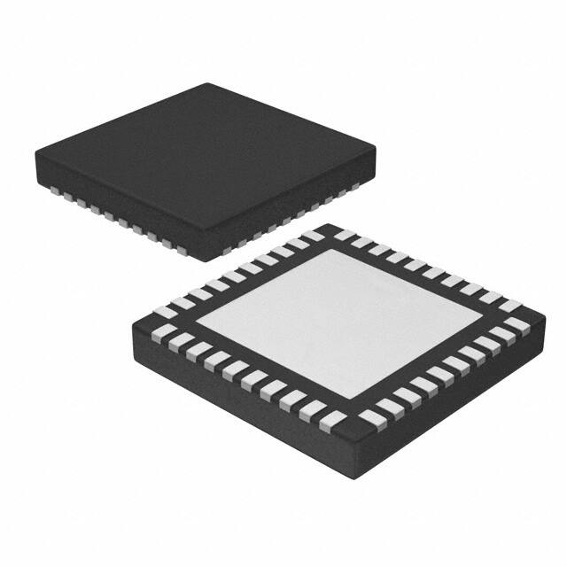
Small, Thermally Efficient 40-Pin 6-mm x 6-mm
RHA (QFN) package
-40°C to 125°C Junction Temperature Range
DESCRIPTION/ORDERING INFORMATION
TPS65257 is a power management IC with three step-down buck converters. Both high-side and low-side
MOSFETs are integrated to provide fully synchronous conversion with higher efficiency. The converters are
designed to simplify its application while giving the designer the option to optimize their usage according to the
target application.
The converters can operate in 5-, 9-, 12- or 15-V systems. The output voltage can be set externally using a
resistor divider to any value between 0.8 V and the input supply minus the resistive drops on the converter path.
Each converter features enable pin that allows a delayed start-up for sequencing purposes, soft start pin that
allows adjustable soft-start time by choosing the soft-start capacitor, and a current limit (RLIM) pin that enables
designer to adjust current limit by selecting an external resistor and optimize the choice of inductor. All converters
operate in ‘hiccup mode’: Once an over-current lasting more than 10 ms is sensed in any of the converters, they
will shut down for 10 ms and then the start-up sequencing will be tried again. If the overload has been removed,
the converter will ramp up and operate normally. If this is not the case the converter will see another over-current
event and shuts down again repeating the cycle (hiccup) until the failure is cleared. If an overload condition lasts
for less than 10 ms, only the relevant converter affected will shut-down and re-start and no global hiccup mode
will occur.
The switching frequency of the converters is set by an external resistor connected to ROSC pin. The switching
regulators are designed to operate from 300 kHz to 2.2 MHz. The converters operate with 180° phase between
then to minimize the input filter requirements.
All converters have peak current mode control which simplifies external frequency compensation. The device has
a built-in slope compensation ramp. The slope compensation can prevent sub harmonic oscillations in peak
current mode control. A traditional type II compensation network can stabilize the system and achieve fast
transient response. Moreover, an optional capacitor in parallel with the upper resistor of the feedback divider
provides one more zero and makes the crossover frequency over 100 kHz.
All converters feature an automatic low power pulse PFM skipping mode which improves efficiency during light
loads and standby operation, while guaranteeing a very low output ripple, allowing for a value of less than 2% at
low output voltages.
1
Please be aware that an important notice concerning availability, standard warranty, and use in critical applications of
Texas Instruments semiconductor products and disclaimers thereto appears at the end of this data sheet.
PRODUCTION DATA information is current as of publication date.
Products conform to specifications per the terms of the Texas
Instruments standard warranty. Production processing does not
necessarily include testing of all parameters.
Copyright © 2011–2012, Texas Instruments Incorporated
�TPS65257
SLVSB32A – SEPTEMBER 2011 – REVISED DECEMBER 2012
www.ti.com
The device incorporates an overvoltage transient protection circuit to minimize voltage overshoot. The OVP
feature minimizes the output overshoot by implementing a circuit to compare the FB pin voltage to OVP threshold
which is 109% of the internal voltage reference. If the FB pin voltage is greater than the OVTP threshold, the
high side MOSFET is disabled preventing current from flowing to the output and minimizing output overshoot.
When the FB voltage drops lower than the OVP lower threshold which is 107%, the high side MOSFET is
allowed to turn on the next clock cycle.
TPS65257 features a supervisor circuit which monitors each buck’s output and the PGOOD pin is asserted once
sequencing is done. The PGOOD pin is an open drain output. The PGOOD pin is pulled low when any buck
converter is pulled below 85% of the nominal output voltage. The PGOOD is pulled up when all converter outputs
are more than 90% of its nominal output voltage. The default reset time is 100 ms. The polarity of the PGOOD is
active high.
The push button operation has been designed to allow for automatic system start when the input supply is
applied or to provide an integrated ON/OFF system management without the need of additional external
components. The behavior of the device will depend on the status of the INT pin (see start-up signals).
The USB switch provides up to 1-A of current as required by downstream USB devices. When the output load
exceeds the current-limit threshold or a short is present, the PMU limits the output current to a safe level by
switching into a constant-current mode and pulling the over current logic output low. When continuous heavy
overloads and short circuits increase the power dissipation in the switch, causing the junction temperature to rise,
a thermal warning protection circuit shuts off the USB switch and allows the buck converters to carry on
operating.
The device implements an internal thermal shutdown to protect itself if the junction temperature exceeds 160°C.
The thermal shutdown forces the device to stop operating when the junction temperature exceeds thermal trip
threshold. Once the die temperature decreases below 140°C, the device reinitiates the power up sequence. The
thermal shutdown hysteresis is 20°C.
ORDERING INFORMATION (1)
PACKAGE (2)
TA
-40°C to 125°C
(1)
(2)
2
40-Pin (QFN) - RHA
PART NUMBER
Reel of 2500
TPS65257RHAR
Reel of 250
TPS65257RHAT
TOP-SIDE MARKING
TPS65257
For the most current packaging and ordering information, see the Package Option Addendum at the end of this document, or see the TI
web site at www.ti.com.
Package drawings, thermal data, and symbolization are available at www.ti.com/packaging.
Submit Documentation Feedback
Copyright © 2011–2012, Texas Instruments Incorporated
Product Folder Links: TPS65257
�TPS65257
www.ti.com
SLVSB32A – SEPTEMBER 2011 – REVISED DECEMBER 2012
This integrated circuit can be damaged by ESD. Texas Instruments recommends that all integrated circuits be handled with
appropriate precautions. Failure to observe proper handling and installation procedures can cause damage.
ESD damage can range from subtle performance degradation to complete device failure. Precision integrated circuits may be more
susceptible to damage because very small parametric changes could cause the device not to meet its published specifications.
FUNCTIONAL BLOCK DIAGRAM
Submit Documentation Feedback
Copyright © 2011–2012, Texas Instruments Incorporated
Product Folder Links: TPS65257
3
�TPS65257
SLVSB32A – SEPTEMBER 2011 – REVISED DECEMBER 2012
www.ti.com
TYPICAL APPLICATION
VPULL
EOR
HOST
SS2
RLIM2
FB2
CMP2
INT
F_PWM
V7V
PGOOD
V3V
GND
IC
FB2
Host
V7V
FB2
EN2
USB_I
USB_VIN
BST2
USB_O
USB_Vo
V2
Host
LX2
USB_EN
VPULL
LX2
TPS65257
USB_nFAULT
V3
LX3
LX1
VIN3
VIN1
BST3
BST1
EN3
EN1
VIN3
RLIM1
SS1
CMP1
FB1
FB1
FB1
ROSC
PB_IN
FB3
FB3
CMP3
SS3
RLIM3
VIN 1
V3V3
4
V1
LX1
LX3
FB3
VIN 2
VIN2
Submit Documentation Feedback
Optional
Copyright © 2011–2012, Texas Instruments Incorporated
Product Folder Links: TPS65257
�TPS65257
www.ti.com
SLVSB32A – SEPTEMBER 2011 – REVISED DECEMBER 2012
GND
V3V
V7V
PGOOD
INT
F_PWM
FB 2
COMP2
SS2
RL IM2
PIN OUT
30
29
28
27
26
25
24
23
22
21
IC
31
20
EN2
USB _Vin
32
19
BST 2
USB _Vo
33
18
VIN2
USB_EN
34
17
LX 2
USB_nFAULT
35
16
LX2
LX3
36
15
LX1
LX3
37
14
LX1
VIN 3
38
13
VIN1
BST 3
39
12
BST1
EN3
40
11
EN1
TPS 65257
2
3
4
5
6
7
8
9
SS3
COMP3
FB 3
PB_IN
ROSC
FB 1
COMP1
SS1
10
RLIM1
1
RLIM3
QFN RHA 40
Submit Documentation Feedback
Copyright © 2011–2012, Texas Instruments Incorporated
Product Folder Links: TPS65257
5
�TPS65257
SLVSB32A – SEPTEMBER 2011 – REVISED DECEMBER 2012
www.ti.com
TERMINAL FUNCTIONS
NAME
NO.
I/O
DESCRIPTION
RLIM3
1
I
Current limit setting for Buck3. Fit a resistor from this pin to ground to set
the peak current limit on the output inductor.
SS3
2
I
Soft start pin for Buck3. Fit a small ceramic capacitor to this pin to set the
converter soft start time.
COMP3
3
O
Compensation for Buck3. Fit a series RC circuit to this pin to complete
the compensation circuit of this converter.
FB3
4
I
Feedback pin for Buck3. Connect a divider set to 0.8 V from the output of
the converter to ground.
PB_IN
5
I
Push button input (active low)
ROSC
6
I
Oscillator set. This resistor sets the frequency of internal autonomous
clock.
FB1
7
I
Feedback pin for Buck1. Connect a divider set to 0.8 V from the output of
the converter to ground.
COMP1
8
O
Compensation pin for Buck1. Fit a series RC circuit to this pin to complete
the compensation circuit of this converter.
SS1
9
I
Soft-start pin for Buck1. Fit a small ceramic capacitor to this pin to set the
converter soft-start time.
RLIM1
10
I
Current limit setting pin for Buck1. Fit a resistor from this pin to ground to
set the peak current limit on the output inductor.
EN1
11
I
Enable pin for Buck1. A high signal on this pin enables the regulator
Buck. For a delayed start-up add a small ceramic capacitor from this pin
to ground.
BST1
12
VIN1
13
I
Input supply for Buck1. Fit a 10-µF ceramic capacitor close to this pin.
LX1
14, 15
O
Switching node for Buck1
LX2
16, 17
O
Switching node for Buck2
VIN2
18
I
Input supply for Buck2. Fit a 10-µF ceramic capacitor close to this pin.
BST2
19
EN2
20
I
Enable pin for Buck2. A high signal on this pin enables the regulator. For
a delayed start-up add a small ceramic capacitor from this pin to ground.
RLIM2
21
I
Current limit setting pin for Buck2. Fit a resistor from this pin to ground to
set the peak current limit on the output inductor.
SS2
22
I
Soft-start pin for Buck2. Fit a small ceramic capacitor to this pin to set the
converter soft-start time.
COMP2
23
O
Compensation pin for Buck2. Fit a series RC circuit to this pin to complete
the compensation circuit of this converter.
FB2
24
I
Feedback input for Buck2. Connect a divider set to 0.8 V from the output
of the converter to ground.
F_PWM
25
INT
26
O
Open drain interrupt output
PGOOD
27
O
Power good. Open drain output asserted low after all converters and
sequenced and within regulation. Polarity is factory selectable (active high
default).
V7V
28
O
Internal supply. Connect a 4.7-μF to 10-μF ceramic capacitor from this pin
to ground.
V3V
29
O
Internal supply. Connect a 3.3-μF to 10-μF ceramic capacitor from this pin
to ground.
GND
30
IC
31
I
This pin should be connected to V7V pin
USB_VIN
32
I
USB switch Input supply
USB_Vo
33
USB_EN
34
6
Bootstrap capacitor for Buck1. Fit a 47-nF ceramic capacitor from this pin
to the switching node.
Bootstrap capacitor for Buck2. Fit a 47-nF ceramic capacitor from this pin
to the switching node.
Forces PWM operation in all converters when set high. If low converters
will operate in automatic PFM/PWM mode.
Ground
USB switch output
I
Enable input, high turns on the switch
Submit Documentation Feedback
Copyright © 2011–2012, Texas Instruments Incorporated
Product Folder Links: TPS65257
�TPS65257
www.ti.com
SLVSB32A – SEPTEMBER 2011 – REVISED DECEMBER 2012
TERMINAL FUNCTIONS (continued)
NAME
NO.
I/O
DESCRIPTION
35
I
USB1 fault flag output, open drain, active low. Asserted when overcurrent
or overtemperature condition is detected in the switch.
LX3
36, 37
O
Switching node for Buck3
VIN3
38
I
Input supply for Buck3. Fit a 10-µF ceramic capacitor close to this pin.
BST3
39
I
Bootstrap capacitor for Buck3. Fit a 47-nF ceramic capacitor from this pin
to the switching node.
EN3
40
I
Enable pin for Buck3. A high signal on this pin enables the converter. For
a delayed start-up add a small ceramic capacitor from this pin to ground.
USB_nFAULT
PowerPAD. Connect to system ground for electrical and thermal
connection.
PowerPAD
ABSOLUTE MAXIMUM RATINGS
(1)
over operating free-air temperature range (unless otherwise noted, all voltages are with respect to GND)
Voltage range at VIN1,VIN2, VIN3, LX1, LX2, LX3
–0.3 to 18
V
Voltage range at LX1, LX2, LX3 (maximum withstand voltage transient < 10 ns)
–3 to 18
V
Voltage at BST1, BST2, BST3 referenced to LX pin
–0.3 to 7
V
Voltage at V7V, COMP1, COMP2, COMP3, USB_Vin, USB_Vo
–0.3 to 7
V
Voltage at V3V, RLIM1, RLIM2, RLIM3, EN1,EN2, EN3, SS1, SS2, SS3, FB1, FB2, FB3 ,
PGOOD, ROSC, PB_IN INT, USB_EN, USB_ILIM, F_PWM
–0.3 to 3.6
V
Voltage at GND
–0.3 to 0.3
V
TJ
Operating junction temperature range
–40 to 125
°C
TSTG
Storage temperature range
–55 to 150
°C
(1)
Stresses beyond those listed under "absolute maximum ratings" may cause permanent damage to the device. These are stress ratings
only, and functional operation of the device at these or any other conditions beyond those indicated under "recommended operating
conditions" is not implied. Exposure to absolute–maximum–rated conditions for extended periods may affect device reliability.
RECOMMENDED OPERATING CONDITIONS
over operating free-air temperature range (unless otherwise noted)
MIN
NOM
MAX
UNIT
VIN
Input operating voltage
4.5
16
V
TA
Junction temperature
–40
85
°C
ELECTROSTATIC DISCHARGE (ESD) PROTECTION
MIN
Human body model (HBM), PB_IN pin to ground
MAX
UNIT
10000
Any other pin
V
2000
Charge device model (CDM)
500
V
PACKAGE DISSIPATION RATINGS (1)
(1)
PACKAGE
θJA (°C/W)
TA = 25°C
POWER RATING (W)
TA = 55°C
POWER RATING (W)
TA = 85°C
POWER RATING (W)
RHA
30
3.33
2.3
1.3
Based on JEDEC 51.5 HIGH K environment measured on a 76.2 x 114 x 0.6-mm board with the following layer arrangement:
(a) Top layer: 2 Oz Cu, 6.7% coverage
(b) Layer 2: 1 Oz Cu, 90% coverage
(c) Layer 3: 1 Oz Cu, 90% coverage
(d) Bottom layer: 2 Oz Cu, 20% coverage
Submit Documentation Feedback
Copyright © 2011–2012, Texas Instruments Incorporated
Product Folder Links: TPS65257
7
�TPS65257
SLVSB32A – SEPTEMBER 2011 – REVISED DECEMBER 2012
www.ti.com
ELECTRICAL CHARACTERISTICS
TJ = –40°C to 125°C, VIN = 12 V, fSW = 500 kHz (unless otherwise noted)
PARAMETER
TEST CONDITIONS
MIN
TYP
MAX
UNIT
INPUT SUPPLY UVLO AND INTERNAL SUPPLY VOLTAGE
VIN
Input voltage range
IDDSDN
Shutdown
EN pin = low for all converters
170
µA
Quiescent (push-button pull-up
current not included)
Converters enabled, no load
Buck1 = 1.2 V
Buck2 = 1.8 V
Buck3 = 3.3 V
TA = 25°C, F_PWM = Low
600
µA
Quiescent, forced PWM
Converters enabled, no load
F_PWM = High
18
mA
IDDQ
UVLO
4.5
VIN under voltage lockout
UVLODEGLITCH
V3p3
Internal biasing supply
I3V
Biasing supply output current
V7V
Internal biasing supply
I7V
Biasing supply output current
V7VUVLO
UVLO for internal V7V rail
16
Rising VIN
4.22
Falling VIN
4.1
Both edges
110
V
µs
3.3
VIN = 12 V
V
10
mA
10
mA
6.25
VIN = 12 V
V7VUVLO_DEGLITCH
Rising V7V
3.8
Falling V7V
3.6
Falling edge
110
V
V
V
µs
BUCK CONVERTERS (ENABLE CIRCUIT, CURRENT LIMIT, SOFT-START AND SWITCHING FREQUENCY)
Enable threshold high
V3p3 = 3.2 V - 3.4 V,
VENx rising
Enable high level
External GPIO, VENX rising
Enable threshold low
V3p3 = 3.2 V - 3.4 V,
VENx falling
Enable low level
External GPIO, VENX falling
VIH_F_PWM
Enable threshold high
V3p3 = 3.2 V - 3.4 V,
VENx rising
VIL_F_PWM
Enable treshold low
V3p3 = 3.2 V - 3.4 V,
VENx falling
ICHEN
Pull up current enable pin
tD
Discharge time enable pins
ISS
Soft-start pin current source
FSW_BK
Converter switching frequency range
RFSW
Frequency setting resistor
fSW_TOL
Internal oscillator accuracy
VIH
VIL
1.55
1.82
V
0.66 x
V3p3
0.98
1.24
0.33 x
V3p3
0.66 x
V3p3
V
0.33 x
V3p3
Power-up
Set externally with resistor
fSW = 800 kHz
V
V
1
µA
10
ms
5
µA
0.3
2.2
MHz
50
600
kΩ
-10
10
%
FEEDBACK, REGULATION, OUTPUT STAGE
VFB
Feedback voltage
tON_MIN
Minimum on time (current sense
blanking)
VIN = 12 V , TA = 25°C
-1%
0.8
1%
VIN = 4.5 V to 16 V
-2%
0.8
2%
135
V
ns
MOSFET (BUCK 1)
H.S. Switch
On resistance of high side FET on
CH1
25°C, BOOT = 6.5 V
95
mΩ
L.S. Switch
On resistance of low side FET on
CH1
25°C, VIN = 12 V
50
mΩ
8
Submit Documentation Feedback
Copyright © 2011–2012, Texas Instruments Incorporated
Product Folder Links: TPS65257
�TPS65257
www.ti.com
SLVSB32A – SEPTEMBER 2011 – REVISED DECEMBER 2012
ELECTRICAL CHARACTERISTICS (continued)
TJ = –40°C to 125°C, VIN = 12 V, fSW = 500 kHz (unless otherwise noted)
PARAMETER
TEST CONDITIONS
MIN
TYP
MAX
UNIT
MOSFET (BUCK 2)
H.S. Switch
On resistance of high side FET on
CH2
25°C, BOOT = 6.5 V
120
mΩ
L.S. Switch
On resistance of low side FET on
CH2
25°C, VIN = 12 V
80
mΩ
H.S. Switch
On resistance of high side FET on
CH3
25°C, BOOT = 6.5 V
120
mΩ
L.S. Switch
On resistance of low side FET on
CH3
25°C, VIN = 12 V
80
mΩ
MOSFET (BUCK 3)
ERROR AMPLIFIER
gM
Error amplifier transconductance
-2 µA < ICOMP < 2 µA
130
µ℧
gmPS
COMP to ILX gm
ILX = 0.5 A
10
A/V
POWER GOOD RESET GENERATOR
VUVBUCKX
Threshold voltage for buck under
voltage
tUV_deglitch
Deglitch time (both edges)
tON_HICCUP
Hiccup mode ON time
tOFF_HICCUP
Hiccup mode OFF time
VOVBUCKX
Threshold voltage for buck over
voltage
tRP
minimum reset period
Output falling
85
Output rising (PG will be
asserted)
90
%
11
ms
VUVBUCKX asserted
12
ms
All converters disabled. Once
tOFF_HICCUP elapses, all
converters will go through
sequencing again.
20
ms
Output rising (high side FET will
be forced off)
109
Output falling (high side FET will
be allowed to switch )
107
Measured after the later of
Buck1 or Buck3 power-up
successfully
100
%
ms
PB_IN
0.33x
V3p3
Low, V3p3 = 3.2-3.4V
VPB
PB_IN, P_OFF , threshold
High, V3p3 = 3.2-3.4V
TPB_DEGLITCH
0.66x
V3p3
POFF Internal de-bounce time turn_on
and turn_off
20
V
ms
USB SWITCH
VINUSB
USB input voltage range
3
VIH_USB_EN
USB_EN high level input voltage
V3p3 = 3.2-3.4 V, VUSB_EN rising
VIL_USB_EN
USB_EN low level input voltage
V3p3 = 3.2-3.4 V, VUSB_EN falling
RDS_USB
Static drain-source on-state
resistance
USB_VIN = 5 V and
Io_USB = 0.5 A, TJ = 2 5°C
ICS_USB
USB current limit
Increasing USB_Vo current
di/dt
DI OUT 2 × Lo
Vout × DVout
(4)
The following equation calculates the minimum output capacitance needed to meet the output voltage ripple
specification.
1
1
×
Co >
8 × fsw VRIPPLE
I RIPPLE
(5)
Where fSW is the switching frequency, VRIPPLE is the maximum allowable output voltage ripple, and VRIPPLE is the
inductor ripple current.
Input Capacitor
A minimum 10-µF X7R/X5R ceramic input capacitor is recommended to be added between VIN and GND of
each converter. The input capacitor must handle the RMS ripple current shown in the following equation.
Icirms = Iout ×
Vout (Vin min - Vout )
×
Vin min
Vin min
(6)
Bootstrap Capacitor
The device has two integrated boot regulators and requires a small ceramic capacitor between the BST and LX
pins to provide the gate drive voltage for the high side MOSFET. The value of the ceramic capacitor should be
0.047 µF. A ceramic capacitor with an X7R or X5R grade dielectric is recommended because of the stable
characteristics over temperature and voltage.
Push Button
The push button control is an optional feature. The user can power on and off the PMU without push button by
connecting the PB pin to GND. Alternatively, the user can power on and off the PMU by using a push button
on/off controller. When the 3.3V LDO’s output is more than 2.6V, the internal logic will detect the voltage at PB to
determine whether the PB pin is used. When the voltage at PB is zero, the PMU will be activated after detecting
PB staying low for at least 20ms. On the other hand, if the voltage at PB is high, the PMU will keep off until the
first solid push button signal. After a valid push button signal is asserted, the PMU will follow each dc/dc
converter’s EN and power up from a valid push button signal.
During power off, once the PB has been pressed, INT is switched low. This warns the system to shut down all
housekeeping tasks. During the off period, the PMU will keep off until a new PB signal is received. This “off”
state can be overridden by recycling the input power.
18
Submit Documentation Feedback
Copyright © 2011–2012, Texas Instruments Incorporated
Product Folder Links: TPS65257
�TPS65257
www.ti.com
SLVSB32A – SEPTEMBER 2011 – REVISED DECEMBER 2012
Turn On Through Push Button
When the PB pin is not tied to GND, a high to low transition on PB initiates the power on sequence. PB must
stay low for a period of 20ms. Once completing this 20mS, the internal EN is asserted and the PMU is turned on.
PB
De-bouncing
20 mS
Internal
EN
Figure 39. Push Button Turn On
Turn Off Through Push Button
A high to low transition on PB initiates the power off sequence. PB must stay low for a period of 20ms. After
completing 20ms, the PMU pulls down the INT to alert the system that the PMU will be shut down within
1024ms. After 1024ms, the PMU will be disabled through an internal EN, which can override the individual EN of
each power converter. The PMU will keep off unless there is another from high to low transition on PB or the
input power is recycled.
De-bouncing
20 mS
PB
200 mS
INT
1024 mS
Internal
EN
Figure 40. Push Button Trun Off
Delayed Start-Up After pb_in
If a delayed start-up is required on any of the buck converters fit a ceramic capacitor to the ENx pins. The delay
added is ~1.67 ms per nF connected to the pin. Note that the EN pins have a weak 1 MΩ pull-up to the 3V3 rail.
Submit Documentation Feedback
Copyright © 2011–2012, Texas Instruments Incorporated
Product Folder Links: TPS65257
19
�TPS65257
SLVSB32A – SEPTEMBER 2011 – REVISED DECEMBER 2012
www.ti.com
VIN
V7 V
V3 V
PB_in
De-bouncing
20 mS
De-bouncing
20 mS
200 mS
INT
1024 mS
Internal EN
EN treshold
Enx rise time
dictated by CEN
EN1
EN2
EN3
All bucks are disabled
Enable discharge
10-12 mS
Pre-bias timing
4-5 mS
PG asserted
BUCK 1
BUCK 2
Pre-biased output
Soft star rise time
dictated by CSS
BUCK 3
Soft start timer
10 ms watchdog
PGOOD
PG timer
100ms
Figure 41. Delayed Start-Up
Out-of-Phase Operation
In order to reduce input ripple current, buck 1 and buck 2 operate 180 degree out-of-phase. This enables the
system having less input ripple, then to lower component cost, save board space and reduce EMI.
Soft-Start Time
The device has an internal pull-up current source of 5 µA that charges an external soft-start capacitor to
implement a slow start time. Equation 7 shows how to select a soft-start capacitor based on an expected slow
start time. The voltage reference (VREF) is 0.8 V and the soft-start charge current (Iss) is 5 µA. The soft-start
circuit requires 1 nF per around 167 µs to be connected at the SS pin. A 0.8-ms soft-start time is implemented for
all converters fitting 4.7 nF to the relevant SS pin.
( )
Css(nF)
Tss(ms) = VREF(V) · Iss(µA)
(7)
The Power Good circuit for the bucks has a 10-ms watchdog. Therefore the soft-start time should be lower than
this value. It is recommended not to exceed 5 ms.
20
Submit Documentation Feedback
Copyright © 2011–2012, Texas Instruments Incorporated
Product Folder Links: TPS65257
�TPS65257
www.ti.com
SLVSB32A – SEPTEMBER 2011 – REVISED DECEMBER 2012
Adjusting the Output Voltage
The output voltage is set with a resistor divider from the output node to the FB pin. It is recommended to use 1%
tolerance or better divider resistors. In order to improve efficiency at light load, start with a value close to 40 kΩ
for the R1 resistor and use Equation 8 to calculate R2.
æ 0.8V ö
R 2 = R1 × ç
÷
è VO - 0.8V ø
(8)
Vo
TPS65257
R1
FB
R2
0.8V
+
Figure 42. Voltage Divider Circuit
Loop Compensation
TPS65257 is a current mode control DC/DC converter. The error amplifier is a transconductance amplifier with a
gM of 130 µA/V. A typical compensation circuit could be type II (Rc and Cc) to have a phase margin between 60°
and 90°, or type III (Rc and Cc and Cff to improve the converter transient response. CRoll adds a high frequency
pole to attenuate high-frequency noise when needed. It may also prevent noise coupling from other rails if there
is possibility of cross coupling in between rails when layout is very compact.
VO
iL
CO
RL
RESR
Gm = 12 A/V
Cff
R1
Current Sense
I/V Gain
FBx
g M = 130 m
VREF = 0.8 V
COMPx
R2
RC
CRoll
CC
Figure 43. Loop Compensation Scheme
Submit Documentation Feedback
Copyright © 2011–2012, Texas Instruments Incorporated
Product Folder Links: TPS65257
21
�TPS65257
SLVSB32A – SEPTEMBER 2011 – REVISED DECEMBER 2012
www.ti.com
To calculate the external compensation components follow the following steps:
TYPE II CIRCUIT
TYPE III CIRCUIT
Select switching frequency that is appropriate for
application depending on L, C sizes, output ripple, EMI
concerns and etc. Switching frequencies around 500 kHz
yield best trade off between performance and cost. When
using smaller L and C, switching frequency can be
increased. To optimize efficiency, switching frequency can
be lowered.
Type III circuit recommended for
switching frequencies higher than
500 kHz.
Select cross over frequency (fc) to be at least 1/5 to 1/10 of
switching frequency (fs).
Suggested
fc = fs/10
RC =
Set and calculate Rc.
2p × fc × Vo × Co
g M × Vref × gm ps
Calculate Cc by placing a compensation zero at or before
the converter dominant pole
Cc =
1
fp =
CO × RL × 2p
Suggested
fc = fs/10
RL × Co
Rc
RC =
2p × fc × Co
g M × gm ps
Cc =
RL × Co
Rc
Add CRoll if needed to remove large signal coupling to high
impedance CMP node. Make sure that
fpRoll =
1
2 × p × RC × CRoll
CRoll =
Re sr × Co
RC
CRoll =
Re sr × Co
RC
is at least twice the cross over frequency.
Calculate Cff compensation zero at low frequency to boost
the phase margin at the crossover frequency. Make sure
that the zero frequency (fzff) is smaller than equivalent
soft-start frequency (1/Tss).
C ff =
NA
1
2 × p × fz ff × R1
Slope Compensation
The device has a built-in slope compensation ramp. The slope compensation can prevent sub harmonic
oscillations in peak current mode control.
Power Good
The PGOOD pin is an open drain output. The PGOOD pin is pulled low when any buck converter is pulled below
85% of the nominal output voltage. The PGOOD is pulled up when both buck converters’ outputs are more than
90% of its nominal output voltage.
The default reset time is 100 ms. The polarity of the PGOOD is active high.
22
Submit Documentation Feedback
Copyright © 2011–2012, Texas Instruments Incorporated
Product Folder Links: TPS65257
�TPS65257
www.ti.com
SLVSB32A – SEPTEMBER 2011 – REVISED DECEMBER 2012
Current Limit Protection
Figure 44 shows the (peak) inductor current limit for Buck 1. The typical limit can be approximated with the
following graph.
Figure 44. Buck 1
Figure 45 shows the (peak) inductor current limit for Buck 2. The typical limit can be approximated with the
following graph.
Figure 45. Buck 2
Submit Documentation Feedback
Copyright © 2011–2012, Texas Instruments Incorporated
Product Folder Links: TPS65257
23
�TPS65257
SLVSB32A – SEPTEMBER 2011 – REVISED DECEMBER 2012
www.ti.com
Figure 46 shows the (peak) inductor current limit for Buck 3. The typical limit can be approximated with the
following graph.
Figure 46. Buck 3
The current limit should be set by using either the TYP or MIN line. If using the TYP line, ensure that limit trips at
the MIN line are acceptable for your application. When setting high-side current limit to large current values,
ensure that the additional load immediately prior to an overcurrent condition will not cause the switching node
voltage to exceed 20 V. Additionally, ensure during worst case operation, with all bucks loaded immediately prior
to current limit, the maximum virtual junction temperature of the device does not exceed 125°C.
All converters operate in hiccup mode: Once an over-current lasting more than 10 ms is sensed in any of the
converters, they will shut down for 10 ms and then the start-up sequencing will be tried again. If the overload has
been removed, the converter will ramp up and operate normally. If this is not the case the converter will see
another over-current event and shuts-down again repeating the cycle (hiccup) until the failure is cleared.
If an overload condition lasts for less than 10 ms, only the relevant converter affected will shut-down and re-start
and no global hiccup mode will occur.
Overvoltage Transient Protection
The device incorporates an overvoltage transient protection (OVP) circuit to minimize voltage overshoot. The
OVP feature minimizes the output overshoot by implementing a circuit to compare the FB pin voltage to OVTP
threshold which is 109% of the internal voltage reference. If the FB pin voltage is greater than the OVTP
threshold, the high side MOSFET is disabled preventing current from flowing to the output and minimizing output
overshoot. When the FB voltage drops lower than the OVTP threshold which is 107%, the high side MOSFET is
allowed to turn on the next clock cycle.
Low Power/Pulse Skipping Operation
When a buck synchronous converter operates at light load or standby conditions, the switching losses are the
dominant source of power losses. Under these load conditions, TPS65257 uses a pulse skipping modulation
technique to reduce the switching losses by keeping the power transistors in the off-state for several switching
cycles, while maintaining a regulated output voltage. Figure 47 shows the output voltage and load plus the
inductor current.
24
Submit Documentation Feedback
Copyright © 2011–2012, Texas Instruments Incorporated
Product Folder Links: TPS65257
�TPS65257
www.ti.com
SLVSB32A – SEPTEMBER 2011 – REVISED DECEMBER 2012
VOUT
IL
Skipping
Burst
IOUT
Figure 47. Low Power/Pulse Skipping
During the burst mode, the converter continuously charges up the output capacitor until the output voltage
reaches a certain limit threshold. The operation of the converter in this interval is equivalent to the peak inductor
current mode control. In each switch period, the main switch is turned on until the inductor current reaches the
peak current limit threshold. As the load increases the number of pulses increases to make sure that the output
voltage stays within regulation limits. When the load is very light the low power controller has a zero crossing
detector to allow the low side mosfet to operate even in light load conditions. The transistor is not disabled at
light loads. A zero crossing detection circuit will disable it when inductor current reverses. During the whole
process the body diode does not conduct but is used as blocking diode only.
During the skipping interval, the upper and lower transistors are turned off and the converter stays in idle mode.
The output capacitors are discharged by the load current until the moment when the output voltage drops to a
low threshold.
The choice of output filter will influence the performance of the low power circuit. The maximum ripple during low
power mode can be calculated as:
K T
VOUT _ RIPPLE = RIP S
COUT
(9)
Where KRIP is 1.4 for Buck1 and 0.7 for Buck2 and Buck3. TS can be calculated as:
0.35
TS =
éæ VIN - VOUT ö VOUT ù
êç
÷ V ú
L
ø IN û
ëè
(10)
USB Switch
The USB switch is enabled (active high) with the USB_EN pin. The switch has a typical resistance of 100mΩ and
has a fold-back current limit that is typically 25% lower than the overcurrent detection point. If a continuous shortcircuit condition is applied to the USB switch output, the USB switch will shut-down once its temperature reaches
130°C, allowing for the buck converters to operate unaffected. Once the USB switch cools down it will restart
automatically.
Submit Documentation Feedback
Copyright © 2011–2012, Texas Instruments Incorporated
Product Folder Links: TPS65257
25
�TPS65257
SLVSB32A – SEPTEMBER 2011 – REVISED DECEMBER 2012
www.ti.com
USB_Vin
0
USB_EN
USB_Vo
OVERCURRENT DETECTED
USB_LOAD
ICS_USB
OVERCURRENT IS CLEARED
USB_I
Normal operation
Overcurrent at the output
. Alarm
is asserted after 5 ms
Normal operation is restored
.
Alarm is cleared
.
USB_nFAULT
T CS_USB
Figure 48. USB Switch
Power Dissipation
The total power dissipation inside TPS65257 should not to exceed the maximum allowable junction temperature
of 125°C. The maximum allowable power dissipation is a function of the thermal resistance of the package (RJA)
and ambient temperature. To calculate the temperature inside the device under continuous loading use the
following procedure:
1. Define the set voltage for each converter.
2. Define the continuous loading on each converter. Make sure do not exceed the converter maximum loading..
3. Determine from the graphs below the expected losses in watts per converter inside the device. The losses
depend on the input supply, the selected switching frequency, the output voltage and the converter chosen.
26
Submit Documentation Feedback
Copyright © 2011–2012, Texas Instruments Incorporated
Product Folder Links: TPS65257
�TPS65257
SLVSB32A – SEPTEMBER 2011 – REVISED DECEMBER 2012
1.6
1.6
1.4
1.4
Expected Power Loss - W
Expected Power Loss - W
www.ti.com
1.2
1
0.8
0.6
1.2
1
0.8
0.6
0.4
0.4
0.2
1
1.2
1.4
1.6
1.8
2
2.2 2.4 2.6
Current - A
2.8
3
3.2
3.4
3.6
0.2
1
1.2
1.4
1.7
1.7
1.6
1.6
1.5
1.5
1.4
1.4
1.3
1.3
1.2
1.1
1
0.9
0.8
0.7
0.6
0.3
0.2
2
2.2
2.4
2.6
3.2
3.4
3.6
0.7
0.6
0.4
1.8
3
0.8
0.3
1.6
2.8
1
0.9
0.5
1.4
2.2 2.4 2.6
Current - A
1.1
0.4
1.2
2
1.2
0.5
1
1.8
Buck1 Vin = 12 V, fsw = 1.1 MHz,
Vo (from top to bottom) = 5, 3.3, 2.5, 1.8, 1.2 V
Expected Power Loss - W
Expected Power Loss - W
Buck1 Vin = 12 V, fsw = 500 kHz,
Vo (from top to bottom) = 5, 3.3, 2.5, 1.8, 1.2 V
1.6
2.8
3
0.2
1
1.2
1.4
1.6
1.8
2
2.2
2.4
2.6
Current - A
Current - A
Buck2&3 Vin = 12 V, fsw = 500 kHz,
Vo (from top to bottom) = 5, 3.3, 2.5, 1.8, 1.2 V
Buck2&3 Vin = 12 V, fsw = 1.1 MHz,
Vo (from top to bottom) = 5, 3.3, 2.5, 1.8, 1.2 V
2.8
3
Figure 49. Power Dissipation Curves
4. To calculate the maximum temperature inside the IC use the following formula:
THOT_SPOT = TA + PDIS x ѲJA
(11)
Where:
TA is the ambient temperature
PDIS is the sum of losses in all converters
ѲJA is the junction to ambient thermal impedance of the device and it is heavily dependant on board layout
Thermal Shutdown
The device implements an internal thermal shutdown to protect itself if the junction temperature exceeds 160°C.
The thermal shutdown forces the device to stop switching when the junction temperature exceeds thermal trip
threshold. Once the die temperature decreases below 140°C, the device reinitiates the power up sequence. The
thermal shutdown hysteresis is 20°C.
3.3-V and 6.5 LDO Regulators
The following ceramic capacitor (X7R/X5R) should be connected as close as possible to the described pins:
• 4.7 µF to 10 µF for V7V pin 28
• 3.3 µF to 10 µF for V3V pin 29
Submit Documentation Feedback
Copyright © 2011–2012, Texas Instruments Incorporated
Product Folder Links: TPS65257
27
�TPS65257
SLVSB32A – SEPTEMBER 2011 – REVISED DECEMBER 2012
www.ti.com
Layout Recommendation
Layout is a critical portion of PMIC designs.
• Place tracing for output voltage and LX on the top layer and an inner power plane for VIN.
• Fit also on the top layer connections for the remaining pins of the PMIC and a large top side area filled with
ground.
• The top layer ground area should be connected to the internal ground layer(s) using vias at the input bypass
capacitor, the output filter capacitor and directly under the TPS65257 device to provide a thermal path from
the PowerPad land to ground.
• For operation at full rated load, the top side ground area together with the internal ground plane, must provide
adequate heat dissipating area.
• There are several signals paths that conduct fast changing currents or voltages that can interact with stray
inductance or parasitic capacitance to generate noise or degrade the power supplies performance. To help
eliminate these problems, the VIN pin should be bypassed to ground with a low ESR ceramic bypass
capacitor with X5R or X7R dielectric. Care should be taken to minimize the loop area formed by the bypass
capacitor connections, the VIN pins, and the ground connections. Since the LX connection is the switching
node, the output inductor should be located close to the LX pins, and the area of the PCB conductor
minimized to prevent excessive capacitive coupling.
• The output filter capacitor ground should use the same power ground trace as the VIN input bypass capacitor.
Try to minimize this conductor length while maintaining adequate width.
• The compensation should be as close as possible to the CMPx pins. The CMPx and ROSC pins are sensitive
to noise so the components associated to these pins should be located as close as possible to the IC and
routed with minimal lengths of trace.
28
Submit Documentation Feedback
Copyright © 2011–2012, Texas Instruments Incorporated
Product Folder Links: TPS65257
�PACKAGE OPTION ADDENDUM
www.ti.com
10-Dec-2020
PACKAGING INFORMATION
Orderable Device
Status
(1)
Package Type Package Pins Package
Drawing
Qty
Eco Plan
(2)
Lead finish/
Ball material
MSL Peak Temp
Op Temp (°C)
Device Marking
(3)
(4/5)
(6)
TPS65257RHAR
ACTIVE
VQFN
RHA
40
2500
RoHS & Green
NIPDAU
Level-3-260C-168 HR
TPS65257RHAT
ACTIVE
VQFN
RHA
40
250
RoHS & Green
NIPDAU
Level-3-260C-168 HR
-40 to 85
TPS
65257
TPS
65257
(1)
The marketing status values are defined as follows:
ACTIVE: Product device recommended for new designs.
LIFEBUY: TI has announced that the device will be discontinued, and a lifetime-buy period is in effect.
NRND: Not recommended for new designs. Device is in production to support existing customers, but TI does not recommend using this part in a new design.
PREVIEW: Device has been announced but is not in production. Samples may or may not be available.
OBSOLETE: TI has discontinued the production of the device.
(2)
RoHS: TI defines "RoHS" to mean semiconductor products that are compliant with the current EU RoHS requirements for all 10 RoHS substances, including the requirement that RoHS substance
do not exceed 0.1% by weight in homogeneous materials. Where designed to be soldered at high temperatures, "RoHS" products are suitable for use in specified lead-free processes. TI may
reference these types of products as "Pb-Free".
RoHS Exempt: TI defines "RoHS Exempt" to mean products that contain lead but are compliant with EU RoHS pursuant to a specific EU RoHS exemption.
Green: TI defines "Green" to mean the content of Chlorine (Cl) and Bromine (Br) based flame retardants meet JS709B low halogen requirements of


 工商网监
湘ICP备2023018690号
工商网监
湘ICP备2023018690号

