TPS65400
SLVSCQ9E – NOVEMBER 2014 – REVISED MARCH 2022
TPS65400 4.5- to 18-V Input Flexible Power Management Unit With PMBus/I2C
Interface
1 Features
2 Applications
•
•
•
•
•
•
•
•
•
•
Efficiency up to 95% for each switching regulator
Switching regulator specifications:
– Input voltage range: 4.5 to 18 V
– VOUT range: 0.6 V-90%VIN
– SW1, SW2 IOUT: 4-A max
– SW3, SW4 IOUT: 2-A max
Prebias start-up algorithm minimizes voltage dip
during start-up
Internal undervoltage lockout (UVLO), overcurrent
protection (OCP), overvoltage protection (OVP),
and overtemperature protection (OTP)
AECQ-100 grade 1 option
Thermally enhanced 7-mm × 7-mm 48-pin, 0.5-mm
pitch VQFN package
Pin accessible features:
– Adjustable VOUT with external feedback
resistors
– Sequencing control through precision enable
pins for each switcher
– Resistor adjustable PWM switching frequency
from 275 kHz to 2.2 MHz
– Clock sync input and clock output
– Soft-start delay through external capacitor
– Current sharing between SW1 and SW2 and
between SW3 and SW4 allows support of
higher current needs if required
PMBus runtime control and status
– Runtime voltage positioning through adjustment
of VREF
– Enable and disable of each switcher
– Fault and status monitoring
User-configurable PMBus/I2C options, saved in
EEPROM
– Power supply turn-on and turn-off sequencing
– Sequencing can be based on fixed time delays
or PGOOD dependence
– Initial voltage positioning through VREF
configuration
– PWM frequency adjustment for each switcher
– Individual PWM phase alignment for each
switcher to minimize ripple and capacitor size
– Adjustable current limit on each regulator
enables size and cost optimization of inductors
– Soft-start time
•
•
•
•
•
Small cellular base stations (BTS) (for example:
picocells and microcells); macro BTS (using
multiple PMUs)
Power over ethernet (PoE) powered
communications infrastructure equipment
Automotive infotainment and telematics
Powering DSP and MCUs
Industrial and factory automation
Systems requiring small form factor, highefficiency, high-ambient operating temperature,
and flexible power management
3 Description
The TPS65400 is an integrated PMU optimized for
applications requiring small form factor and high
power conversion efficiency, enabling small spaceconstrained equipment with high ambient operating
temperature without cooling. The device provides
high-power efficiency at a system level by enabling
a single stage conversion from an intermediate
distribution bus with an optimized combination of
regulators.
Device Information
(1)
PART NUMBER
PACKAGE(1)
BODY SIZE (NOM)
TPS65400
VQFN (48)
7.00 mm × 7.00 mm
For all available packages, see the orderable addendum at
the end of the data sheet.
Vin: 4.5 to 18 V
4A
4A
BUCK1
BUCK4
BUCK2
BUCK3
2A
2A
PMBus/I2C
Simplified Schematic
An IMPORTANT NOTICE at the end of this data sheet addresses availability, warranty, changes, use in safety-critical applications,
intellectual property matters and other important disclaimers. PRODUCTION DATA.
�TPS65400
www.ti.com
SLVSCQ9E – NOVEMBER 2014 – REVISED MARCH 2022
Table of Contents
1 Features............................................................................1
2 Applications..................................................................... 1
3 Description.......................................................................1
4 Revision History.............................................................. 2
5 Description (continued).................................................. 3
6 Pin Configuration and Functions...................................3
7 Specifications.................................................................. 6
7.1 Absolute Maximum Ratings........................................ 6
7.2 ESD Ratings............................................................... 6
7.3 Recommended Operating Conditions.........................6
7.4 Thermal Information....................................................7
7.5 Electrical Characteristics.............................................7
7.6 System Characteristics............................................... 9
7.7 Operational Parameters............................................10
7.8 Package Dissipation Ratings.................................... 10
7.9 Typical Characteristics: System Efficiency................10
8 Detailed Description...................................................... 11
8.1 Overview................................................................... 11
8.2 Functional Block Diagrams....................................... 12
8.3 Feature Description...................................................13
8.4 Device Functional Modes..........................................28
8.5 Programming............................................................ 29
8.6 Register Maps...........................................................34
9 Application and Implementation.................................. 54
9.1 Application Information............................................. 54
9.2 Typical Applications.................................................. 55
10 Power Supply Recommendations..............................67
11 Layout........................................................................... 68
11.1 Layout Guidelines................................................... 68
11.2 Layout Example...................................................... 69
12 Device and Documentation Support..........................70
12.1 Documentation Support.......................................... 70
12.2 Receiving Notification of Documentation Updates..70
12.3 Glossary..................................................................70
12.4 Trademarks............................................................. 70
12.5 Electrostatic Discharge Caution..............................70
12.6 Glossary..................................................................70
13 Mechanical, Packaging, and Orderable
Information.................................................................... 70
4 Revision History
NOTE: Page numbers for previous revisions may differ from page numbers in the current version.
Changes from Revision D (July 2018) to Revision E (March 2022)
Page
• Updated the numbering format for tables, figures, and cross-references throughout the document. ................1
Changes from Revision C (May 2018) to Revision D (July 2018)
Page
• Added soldering and storage temperature ........................................................................................................ 6
• Added minimum value for TJ ..............................................................................................................................6
• Updated the default timing for tON_DELAY and tOFF_DELAY to 5 ms in the External Sequencing section.............14
2
Submit Document Feedback
Copyright © 2022 Texas Instruments Incorporated
Product Folder Links: TPS65400
�TPS65400
www.ti.com
SLVSCQ9E – NOVEMBER 2014 – REVISED MARCH 2022
5 Description (continued)
The TPS65400 implements a PMBus-I2C-compatible digital interface. It helps Core Chip optimize system
performance by run-time changing regulated voltage, power sequence, phase interleaving, operating frequency,
read back operating status, and so forth.
The TPS65400 consists of four high-current buck switching regulators (SW1, SW2, SW3, and SW4) with
integrated FETs. The switching power supplies are intended for powering high-current digital circuits such as the
processor, FPGA, ASIC, memory, and digital I/Os. SW1 and SW2 support 4 A each, and SW3 and SW4 support
2 A each. The switching frequency of each regulator is independently adjustable up to 2.2 MHz.
Current limit programmability on each switcher enables optimization of inductor ratings for a particular
application configuration not requiring the maximum current capability.
The TPS65400 can be powered from a single-input voltage rail between 4.5 and 18 V, making it suitable for
applications running off a 5- or 12-V intermediate power distribution bus.
Sequencing requirements can be met using the individual enable terminals or by programming the sequence
through the I2C bus into the on-board EEPROM. Output voltages can be set through external resistor networks
and VREF can be programmed from 0.6 V to 1.87 V in 10-mV steps. All control and status info can be accessed
through a PMBus-compatible I2C bus.
The TPS65400 provides a high level of flexibility for monitoring and control through the I2C bus while providing
the option of programmability through the use of external components and voltage levels for systems not using
I2C.
CB1
1
SW1
2
SW1
3
SW1
VFB1
COMP1
SS1/PG1
CLK_OUT
SCL
SDA
I2CALERT
RCLOCK_SYNC
RST_N
I2CADDR
SS4/PG4
47
46
45
44
43
42
41
40
39
38
37
ENSW1/ENSEQ
48
6 Pin Configuration and Functions
36
COMP4
35
VFB4
34
ENSW4
4
33
CB4
PVIN1
5
32
SW4
PGND(thermal pad)
A.
23
24
SS3/PG3
COMP3
CE
25
22
12
21
CB2
VIN
VFB3
AGND
26
20
11
VDDD
SW2
19
ENSW3
VDDA
CB3
27
18
28
10
17
9
SW2
VDDG
SW2
PGOOD
SW3
16
29
SS2/PG2
8
15
PGND2
14
PVIN3
VFB2
PVIN4
30
COMP2
31
7
13
6
ENSW2
PVIN2
PGND1
Thermal pad must be soldered to PCB as SW3 and SW4 power ground.
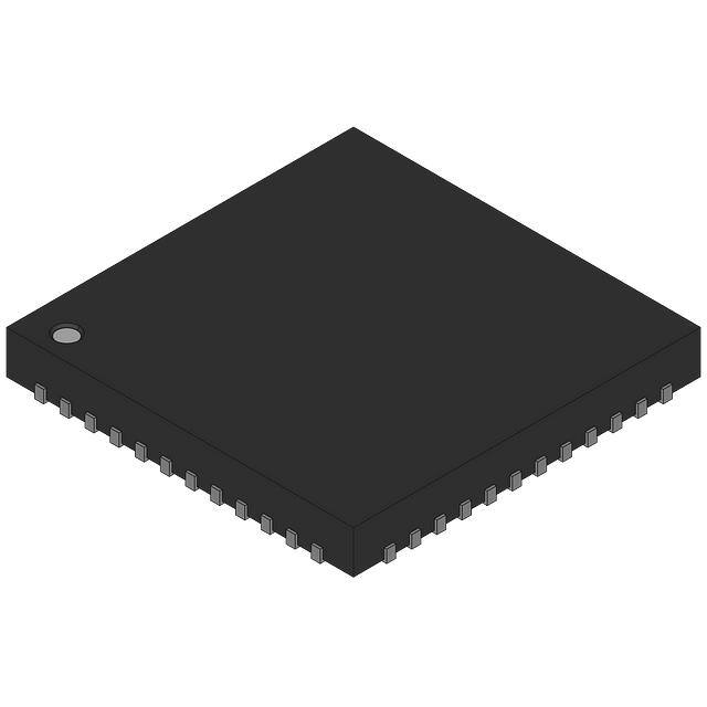
Figure 6-1. 48-Pin VQFN RGZ Package (Top View)
Submit Document Feedback
Copyright © 2022 Texas Instruments Incorporated
Product Folder Links: TPS65400
3
�TPS65400
www.ti.com
SLVSCQ9E – NOVEMBER 2014 – REVISED MARCH 2022
Table 6-1. Pin Functions
PIN
NAME
CB1
DESCRIPTION
NO.
1
Bootstrap pin for the high-side MOSFET gate drive for SW1
2
SW1
3
Switch pin for SW1
4
PVIN1
5
Power input for the buck switching regulator SW1
PVIN2
6
Power input for SW2
PGND1
7
Power ground for buck converters
PGND2
8
Power ground for buck converters
SW2
10
CB2
12
Bootstrap pin for the SW2 high-side MOSFET gate drive
ENSW2
13
Enable input pin for SW2. Active high. A 2-µA internal pullup current is inside.
VFB2
14
Feedback input pin for SW2
COMP2
15
Compensation pin for external compensation network for SW2. Pulling this line high to VDDA configures the
SW1 controller to control both SW1 and SW2.
SS2/PG2
16
Soft start for SW2 (default). A capacitor is used to set the start-up time. This pin can also be reconfigured
through I2C to display the PGOOD2 signal instead.
PGOOD
17
Default PGOOD signal is for all switchers. It can be changed according to (D2h) PIN_CONFIG_00. If all
switchers are disabled, PGOOD is low.
VDDG
18
Supply for gate drives. Bypass locally to PGND.
VDDA
19
Output of internal regulator for analog controls
VDDD
20
3.3-V output of internal regulator digital controls
AGND
21
Ground connection for analog controls
VIN
22
Analog VIN. Power input pin for the VDDD, VDDA, and VGATE subregulator power
CE
23
Chip enables. Internal pullup current will default to high if the pin is left floating. Connect to an open-drain
output to pull low to disable. Driving with a push-pull output is not recommended. When low, internal regulators
are shutdown to minimize power, and functions are disabled. Configuration is reloaded from EEPROM as part
of the power-up sequence when CE goes high.
SS3/PG3
24
Soft-start for SW3 (default). A capacitor is used to set the startup time. This pin can also be reconfigured
through I2C to display the PGOOD3 signal instead.
COMP3
25
Compensation pin for external compensation network for SW3
VFB3
26
Feedback input pin for SW3
ENSW3
27
Enable input pin for SW3. Active high. A 2-µA internal pullup current is inside.
CB3
28
Bootstrap pin for SW3 high-side MOSFET gate drive
SW3
29
Switch pin for SW3. The maximum rated output current is 2 A.
PVIN3
30
Power input for buck switching regulator SW3
PVIN4
31
Power input for SW4
SW4
32
Switch pin for SW4. The maximum rated output current is 2 A.
CB4
33
Bootstrap pin for SW4 high-side MOSFET gate drive
ENSW4
34
Enable input pin for SW4. Active high. A 2-µA internal pullup current is inside.
VFB4
35
Feedback input pin for SW4
COMP4
36
Compensation pin for external compensation network for SW4. Pulling this line high to VDDA configures the
SW3 controller to control both SW3 and SW4.
SS4/PG4
37
Soft start for SW4 (default). A capacitor is used to set the start-up time. This pin can also be reconfigured
through I2C to display the PGOOD4 signal instead.
I2CADDR
38
Select I2C address with a resistor to AGND.
9
Switch pin for SW2
11
4
Submit Document Feedback
Copyright © 2022 Texas Instruments Incorporated
Product Folder Links: TPS65400
�TPS65400
www.ti.com
SLVSCQ9E – NOVEMBER 2014 – REVISED MARCH 2022
Table 6-1. Pin Functions (continued)
PIN
NAME
DESCRIPTION
NO.
RST_N
39
Reset of digital logic. When low, all switchers are disabled. Configuration is reloaded from EEPROM when
RESET_N is deasserted.
RCLOCK_SYNC
40
Resistor for setting primary clock frequency from 275 kHz to 2.2 MHz or for clock sync
I2CALERT
41
Open-drain output that is pulled low for 200 µs when a timeout condition is detected by the I2C watchdog on
either SDA or SCL.
SDA
42
Data input/output pin for I2C bus
SCL
43
Clock input pin for I2C bus
CLK_OUT
44
Clock output signal. Open-collector output, requires pull up
SS1/PG1
45
Soft start for SW1 (default). A capacitor is used to set the start-up time. This pin can also be reconfigured
through I2C to display the PGOOD1 signal instead.
COMP1
46
Compensation pin for external compensation network for SW1
VFB1
47
Feedback input pin for SW1
ENSW1/ENSEQ
48
Enable input pin for SW1. Active high. A 2-µA internal pullup current is inside.
Submit Document Feedback
Copyright © 2022 Texas Instruments Incorporated
Product Folder Links: TPS65400
5
�TPS65400
www.ti.com
SLVSCQ9E – NOVEMBER 2014 – REVISED MARCH 2022
7 Specifications
7.1 Absolute Maximum Ratings
over operating free-air temperature (unless otherwise noted) (1)
MIN
MAX
UNIT
PVIN1, PVIN2, PVIN3, PVIN4, VIN
–0.3
20.0
V
CB1, CB2, CB3, CB4 referenced to SWx
–0.3
7.5
V
CLK_OUT, VFB1, VFB2, VFB3, VFB4, RST_N, I2CALERT, CLK_OUT,
I2CADDR, RCLOCK_SYNC
–0.3
VDDD or 3.6
V
SW1, SW2, SW3, SW4
–1.0
20.0
V
VDDA, VDDG
–0.3
7.5
V
PGOOD, SS1/PG1, SS2/PG2, SS3/PG3, SS4/PG4, COMP1, COMP2,
COMP3, COMP4, CE
–0.3
VDDA or 7.5
V
VDDD
–0.3
3.6
V
SCL, SDA, ENSW1, ENSW2, ENSW3, ENSW4
–0.3
4.0
V
Junction temperature, TJ-max
150
°C
Maximum lead temperature (soldering, 10 s)
260
°C
150
°C
Input voltage
Storage temperature, Tstg
(1)
–55
Stresses beyond those listed under Absolute Maximum Ratings may cause permanent damage to the device. These are stress
ratings only, which do not imply functional operation of the device at these or any other conditions beyond those indicated under
Recommended Operating Conditions. Exposure to absolute-maximum-rated conditions for extended periods may affect device
reliability.
7.2 ESD Ratings
VALUE
V(ESD)
(1)
(2)
Electrostatic
discharge
Human body model (HBM), per ANSI/ESDA/JEDEC JS-001, all
pins(1)
UNIT
±2000
Charged device model (CDM), per JEDEC specification JESD22-C101, all pins(2)
V
±750
JEDEC document JEP155 states that 500-V HBM allows safe manufacturing with a standard ESD control process.
JEDEC document JEP157 states that 250-V CDM allows safe manufacturing with a standard ESD control process.
7.3 Recommended Operating Conditions
over operating free-air temperature range (unless otherwise noted)
Input voltage
MIN
MAX
UNIT
PVIN1, PVIN2, PVIN3, PVIN4, VIN
–0.3
18.0
V
CB1, CB2, CB3, CB4 referenced to SWx
–0.3
7.0
V
ENSW1, ENSW2, ENSW3, ENSW4, SCL, SDA, CLK_OUT, RST_N,
SCL, SDA, I2CALERT, CLK_OUT, I2CADDR, RCLOCK_SYNC, VDDD
–0.3
3.3
V
SW1, SW2, SW3, SW4
–1.0
18.0
V
VDDA, VDDG
–0.3
7.0
V
PGOOD, SS1/PG1, SS2/PG2, SS3/PG3, SS4/PG4, COMP1, COMP2,
COMP3, COMP4, CE
–0.3
7.0
V
0.6
1.87
V
VFB1, VFB2, VFB3, VFB4
Load current
IOUT1, IOUT2
0
4
A
Load current
IOUT3, IOUT4
0
2
A
–40
125
°C
Junction temperature
6
Submit Document Feedback
Copyright © 2022 Texas Instruments Incorporated
Product Folder Links: TPS65400
�TPS65400
www.ti.com
SLVSCQ9E – NOVEMBER 2014 – REVISED MARCH 2022
7.4 Thermal Information
TPS65400
THERMAL
METRIC(1)
UNIT
RGZ (VQFN)
48 PINS
RθJA
Junction-to-ambient thermal resistance
29.8
°C/W
RθJC(top)
Junction-to-case (top) thermal resistance
14.9
°C/W
RθJB
Junction-to-board thermal resistance
6.3
°C/W
ψJT
Junction-to-top characterization parameter
0.2
°C/W
ψJB
Junction-to-board characterization parameter
6.3
°C/W
RθJC(bot)
Junction-to-case (bottom) thermal resistance
0.8
°C/W
(1)
For more information about traditional and new thermal metrics, see the Semiconductor and IC Package Thermal Metrics application
report, SPRA953.
7.5 Electrical Characteristics
VIN = 12 V, Frequency = 500 kHz, TJ = –40°C to 125°C, typical values are at TJ = 25°C, unless otherwise indicated
PARAMETER
TEST CONDITIONS
MIN
TYP
MAX
UNIT
SWITCHER 1 AND SWITCHER 2
Ilimit1, Ilimit2
SW1, SW2 high-side current limit
adjustment range
Ilimit-accuracy
Accuracy to nominal current limit value
Rdson HS
SW1, SW2 HS Rds(on)
66
mΩ
Rdson LS
SW1, SW2 LS Rds(on)
42
mΩ
2
Ilimit = 4 A, 5 A, 6 A
6
–25%
A
25%
SWITCHER 3 AND SWITCHER 4
Ilimit3, Ilimit4
SW3 and SW4 current limit
Ilimit accuracy
Accuracy to nominal current limit value
Rdson HS
SW3 and SW4 HS Rds(on)
Rdson LS
SW3/4 LS Rds(on)
Ilimit = 1 A, 2 A, 3 A
0.5
3
–25%
25%
A
120
mΩ
90
mΩ
FEEDBACK AND ERROR AMPLIFIERS FOR SW1 – SW4
VFB
Accuracy
VREF = 1 V
–1%
VREFn
Error amplifier reference voltage
Default value
VREF_STEP
I2C programmable VREF step size
Gm
Error amplifier transconductance
Isink
Sink
12
µA
Isource
Source
12
µA
95
1%
800
mV
10
mV
133
165
µS
PWM SWITCHING CHARACTERISTICS
Phase_err12(1) Phase error between SW1 and SW2
Fsw = 1.1 MHz
5⁰
Phase_err34(1) Phase error between SW3 and SW4
Fsw = 1.1 MHz
5⁰
Fsw
Resistor-configurable PWM switching
configuration
Fsw-accuracy
PWM switching frequency accuracy
Vrclock_sync
Voltage reference for RCLOCK_SYNC
0.8
tON_min
Lower duty cycle limit
80
tOFF_min
Minimum off-time limit (constrains the
maximum achievable duty cycle)
ROSC = 165 kΩ
(Fsw = 1.1 MHz)
275
2200
–10%
10%
kHz
V
150
150
ns
ns
CLOCK SYNC
V_HSYNC
High signal threshold
V_LSYNC
Low signal threshold
2.6
V
1
V
Submit Document Feedback
Copyright © 2022 Texas Instruments Incorporated
Product Folder Links: TPS65400
7
�TPS65400
www.ti.com
SLVSCQ9E – NOVEMBER 2014 – REVISED MARCH 2022
VIN = 12 V, Frequency = 500 kHz, TJ = –40°C to 125°C, typical values are at TJ = 25°C, unless otherwise indicated
PARAMETER
TEST CONDITIONS
ICLKOUT
Max current sink/source for CLK_OUT
tmin_ SYNC
Minimum detectable time for sync pulse
FSYNC
Frequency synchronization range
TSYNC_DELAY
Delay between input pulse to
RCLOCK_SYNC and rising edge of
CLK_OUT and PWM output
MIN
TYP
MAX
2
275
UNIT
mA
150
ns
2200
kHz
20
ns
20
ms
TIMING CHARACTERISTICS
Delay for restart during repeated OCP
condition
trestart
INTERNAL REGULATORS AND UVLO
VDDA
Internal subregulator output
VDDD
Output of internal subregulator
Vin > 6.6 V
6.1
4.5 V < Vin 6.6 V
V
Vin – 0.1
3.2
Vin > 6.6 V
VDDG
Output of internal regulator for gate
drivers
IVIN
Quiescent non-switching, no load current
CE high, VFB >> VREF, (no
switching)
ISD
Quiescent shutdown current
CE low
VIN_UVLO
Input voltage UVLO
Rising
VIN_UVLO
Input voltage UVLO
Falling
V
6.1
4.5 V < Vin 6.6 V
V
Vin – 0.1
8
3.4
mA
12
27
µA
4.25
4.48
V
3.75
V
PGOOD, ENSWx, RST_N, SSx, PG
R_LPGOOD
Resistance of PGOOD outputs when low
V_OLPGOOD
Logic output low voltage
500
ISS
Soft-start current
4.1
VEN
Enable logic high threshold (for ENSW1,
VEN rising
ENSW2, ENSW3, ENSW4)
VEN_L
Enable logic low threshold (for ENSW1,
EN_L ENSW2, ENSW3, ENSW4)
VEN_HYS
Enable hysteresis (for ENSW1, ENSW2,
VEN falling
ENSW3, ENSW4)
IEN
ENSWx pin pullup current
VEN = 0
ICE
CE pin pullup current
VCE = 0
VIH_CE
Logic input high for CE
VIL_CE
Logic input low CE
VIH_RSTN
Logic input high RST_N
VIL_RSTN
Logic input low RST_N
I_OL = 100 µA
VEN falling
Ω
0.1
V
5.6
7.3
µA
1.12
1.20
1.28
V
0.97
1.07
V
130
mV
2
µA
2
µA
1.3
V
0.4
1.3
V
V
0.4
V
0.8
V
I2C MODULE (SDA, SCL, I2CALERT, I2CADDR)
V_ILI2C
Logic input low SCL, SDA
V_IHI2C
Logic input high for SCL, SDA
R_LI2C
ON resistance of I2C pins (SDA, SCL,
I2CALERT) to GND
I2CALERT = 1
V_OLI2C
Logic output low voltage for SCL, SDA,
I2CALERT pins
I_OL = 350 µA
ILEAK
Input leakage current
SDA, SCL = 3.3 V
II2CADDR
Source current of I2CADDR pin
VDDD = 3.3 V, VIN > 4.5 V
tTIMEOUT
Timeout detection on SDA or SCL low
2.1
tTIMEOUT_PULSE Duration of timeout pulse on I2CALERT
8
Submit Document Feedback
V
85
Ω
0.1
V
1
µA
20
µA
30
ms
200
µs
Copyright © 2022 Texas Instruments Incorporated
Product Folder Links: TPS65400
�TPS65400
www.ti.com
SLVSCQ9E – NOVEMBER 2014 – REVISED MARCH 2022
VIN = 12 V, Frequency = 500 kHz, TJ = –40°C to 125°C, typical values are at TJ = 25°C, unless otherwise indicated
PARAMETER
TEST CONDITIONS
MIN
TYP
MAX
UNIT
FAULTS
TTSD (2)
Thermal shutdown threshold
160
⁰C
TTSD_restart (2)
Thermal shutdown hysteresis
20
⁰C
VFB_OVP
tOVPSDOWN
VFB UVP
tUVPSDOWN
(1)
(2)
OVP threshold rising (fault latched,
PGOOD asserted)
0.6V < VREF < 1.87 V
111
% of VREF
OVP threshold falling (fault cleared,
PGOOD deasserted)
0.6 V < VREF < 1.87 V
104
% of VREF
Time after OVP before protection
activation and PGOOD fall
55
95
µs
Undervoltage threshold (PGOOD
deasserted)
0.6 V < VREF < 1.87 V
92
% of VREF
Undervoltage threshold (PGOOD
asserted)
0.6 V < VREF < 1.87 V
83
% of VREF
Time after UVP before PGOOD fall
55
95
µs
Specified by design
Specified by lab validation
7.6 System Characteristics
The following specification table entries are specified by the design (component values provided in the typical application
circuit are used). These parameters are not specified by production testing. minimum and max values apply over the full
operating ambient temperature range (–40°C ≤ TJ ≤ 125°C), over the VIN range = 5 to 12 V, and IOUT range unless otherwise
specified. L = 3.3 µH, DCR = 10.4 mΩ, VOUT = 1.2 V, 1% FB resistor.
PARAMETER
TEST CONDITIONS
MIN
TYP
MAX
UNIT
VLINEREG
Line regulation
VLOADREG
Load regulation
tr
VOUT step duration (tr)
For 50-mV step
ts
VOUT step settling time (ts)
For 50-mV step
30
µs
VOVUV
VOUT step overshoot/undershoot
For 50-mV step
6
mV
Efficiency (SW1 and SW2)
Efficiency (SW3 and SW4)
%/A
30
µs
VIN = 12 V, VO = 1.2 V, IOUT = 4 A,
ƒsw = 500 kHz
76%
VIN = 5 V, VO = 1.2 V, IOUT = 2 A,
ƒsw= 500 kHz
77%
VIN = 12 V, VO = 1.2 V, IOUT = 2 A,
ƒsw= 500 kHz
74%
IPKmatch
Peak current ((2)) sharing accuracy
(SW1 and SW2, SW3 and SW4)
tacc
Timing accuracy for delays and
restarts
treset_delay
Time after RSTn or CE is released
for power sequence to begin
Default value
Minimum delay after reset is
released for power sequence to
begin
treset_delay set to 0 ms
(1)
(2)
0.1
77%
IOUTmatch
0
%/V
VIN = 5 V, VO = 1.2 V, IOUT = 4 A,
ƒsw = 500 kHz
Average ((1)) current sharing
accuracy (SW1 and SW2, SW3 and Iload = IOUTmax
SW4)
treset_delay_max
0.1
20%
Iload = IOUTmax
20%
–10%
10%
1
ms
1.1
ms
Average current sharing accuracy is highly dependent on the matching of the inductor and capacitor.
Peak current sharing accuracy refers to the max inductor current in each phase.
Submit Document Feedback
Copyright © 2022 Texas Instruments Incorporated
Product Folder Links: TPS65400
9
�TPS65400
www.ti.com
SLVSCQ9E – NOVEMBER 2014 – REVISED MARCH 2022
7.7 Operational Parameters
Values recommended that ensure proper system behavior
PARAMETER
MIN
TYP
MAX
UNIT
CA
Stabilization capacitor to be connected to VDDA
4.7
µF
CD
Stabilization capacitor to be connected to VDDD
3.3
µF
CG
Stabilization capacitor to be connected to VDDG
Vin1, Vin2, Vin3, Vin4
SW1 to SW4 input voltage
4.5
18
V
Vout1, Vout2, Vout3, Vout4
SW1 to SW4 output voltage
0.6
90% of
VIN
V
10
µF
7.8 Package Dissipation Ratings
(1)
PACKAGE
RθJA (°C/W)(1)
TA = 25°C
TA = 55°C
TA = 85°C
RGZ
29.8
4.5 W
3.14 W
1.77 W
For more information about traditional and new thermal metrics, see the Semiconductor and IC Package Thermal Metrics application
report, SPRA953.
100%
100%
90%
90%
80%
80%
70%
70%
60%
60%
Efficiency
Efficiency
7.9 Typical Characteristics: System Efficiency
50%
40%
VIN = 12 V; VOUT = 1V8
VIN = 12 V; VOUT = 1V5
VIN = 12 V; VOUT = 1V2
VIN = 12 V; VOUT = 1V
20%
10%
0
0.5
1
1.5
2
2.5
3
3.5
IOUT
VIN = 5 V; VOUT = 1V8
VIN = 5 V; VOUT = 1V5
VIN = 5 V; VOUT = 1V2
VIN = 5 V; VOUT = 1V
20%
10%
0
0
0
4
0.5
1
1.5
D001
Figure 7-1. Buck1 and Buck2 Power Efficiency, VIN
= 12 V
90%
80%
80%
70%
70%
60%
60%
Efficiency
100%
90%
40%
30%
2.5
3
3.5
4
D002
Figure 7-2. Buck1 and Buck2 Power Efficiency, VIN
=5V
100%
50%
2
IOUT
With 500 kHz and XAL6060-472 4.7-µH, 13.2-mΩ inductor
With 500 kHz and XAL6060-472 4.7-µH, 13.2-mΩ inductor
Efficiency
40%
30%
30%
50%
40%
30%
VIN = 12 V; VOUT = 1V8
VIN = 12 V; VOUT = 1V5
VIN = 12 V; VOUT = 1V2
VIN = 12 V; VOUT = 1V
20%
10%
VIN = 5 V; VOUT = 1V8
VIN = 5 V; VOUT = 1V5
VIN = 5 V; VOUT = 1V2
VIN = 5 V; VOUT = 1V
20%
10%
0
0
0
0.25
0.5
0.75
1
1.25
1.5
1.75
IOUT
2
0
0.25
D004
With 500 kHz FSW and 4.7-µH, 34-mΩ inductor
Figure 7-3. Buck3 and Buck4 Power Efficiency, VIN
= 12 V
10
50%
0.5
0.75
1
IOUT
1.25
1.5
1.75
2
D001
With 500 kHz FSW and 4.7-µH, 34-mΩ inductor
Figure 7-4. Buck3 and Buck4 Power Efficiency, VIN
=5V
Submit Document Feedback
Copyright © 2022 Texas Instruments Incorporated
Product Folder Links: TPS65400
�TPS65400
www.ti.com
SLVSCQ9E – NOVEMBER 2014 – REVISED MARCH 2022
8 Detailed Description
8.1 Overview
The TPS65400 is an integrated PMU optimized for applications that require small form factor and high-power
conversion efficiency enabling small space-constrained equipment with high-ambient operating temperature
without cooling. It provides high-power efficiency at a system level by enabling a single-stage conversion from an
intermediate distribution bus with an optimized combination of regulators.
The TPS65400 consists of four high-current buck-switching regulators (SW1, SW2, SW3, and SW4) with
integrated FETs. The switching power supplies are intended for powering high-current digital circuits such as
the processor, FPGA, ASIC, memory, and digital I/Os. SW1 and SW2 support 4 A each, and SW3 and SW4
support 2 A each. Each regulator’s switching frequency is independently adjustable up to 2.2 MHz.
Current limit programmability on each switcher enables optimization of inductor ratings for a particular
application configuration not requiring the maximum current capability.
The TPS65400 can be powered from a single-input voltage rail between 4.5 and 18 V, making it suitable for
applications running off a 5- or 12-V intermediate power distribution bus.
Sequencing requirements can be met using the individual enable pins or by programming the sequence through
the I2C bus into the onboard EEPROM. Output voltages can be set through external resistor networks and VREF
can be programmed from 0.6 to 1.87 V in 10-mV steps. All control and status info can be accessed through a
PMBus-compatible I2C bus.
The TPS65400 provides a high level of flexibility for monitoring and control through the I2C bus while providing
the option of programmability through the use of external components and voltage levels for systems not using
I2C.
Submit Document Feedback
Copyright © 2022 Texas Instruments Incorporated
Product Folder Links: TPS65400
11
�TPS65400
www.ti.com
SLVSCQ9E – NOVEMBER 2014 – REVISED MARCH 2022
8.2 Functional Block Diagrams
COMP2
COMP1
PVIN1
SS DAC VREF DAC
SDA
SCL
I2C
I2CADDR
EEPROM
and
Charge Pump
PWM Controller
CB1
Gate Driver
SW1
I2CALERT
RCLOCK_SYNC
CLOCK
(Adj Fsw and )
OVP
UVP
OCP
ISENSE
VFB1
CLK_OUT
PVIN2
ENSW1
ENSW2
ENSW3
ENSW4
PGND1
Enable
and
PGOOD
Sequencing
Controller
SS DAC VREF DAC
PWM Controller
CB2
Gate Driver
SW2
PGOOD
OVP
UVP
SS1/PG1
SS2/PG2
SS3/PG3
Soft-Start
or
PGOOD#
OCP
ISENSE
PGND2
VFB2
TPS65400
SS4/PG4
PVIN3
CB3
SS DAC VREF DAC
RST_N
PWM Controller
CE
VIN
OVP
UVP
VDDD
VDDA
VDDG
Internal
Sub-Reg
and
Bias
AGND
Gate Driver
OCP
ISENSE
PWM Controller
OVP
UVP
COMP3
PGND (Thermal Pad)
VFB3
PVIN4
CB4
SS DAC VREF DAC
VREF
UVLO
OTP
SW3
Gate Driver
OCP
ISENSE
SW4
PGND (Thermal Pad)
VFB4
COMP4
Figure 8-1. TPS65400 Functional Block Diagram
12
Submit Document Feedback
Copyright © 2022 Texas Instruments Incorporated
Product Folder Links: TPS65400
�TPS65400
www.ti.com
SLVSCQ9E – NOVEMBER 2014 – REVISED MARCH 2022
INPUT+
VDDG
VIN
VDDA
VDDD
VDDA
Regulator
RCLOCK_SYNC
VDDG
Regulator
0
PVIN1
Oscillator
CB1
VDDD
Regulator
UVLO
VREF1
Generator
VREF1
SS1
OUTPUT+
UVLO
COMP
Precharge
OVP1
SW1
Logic
GM1
FB1
0.5V
COMP1
OVP1/UVP1
Detector
Slope
Comp.1
OCP1
High Side
Current
Sense
Zero Cross
Detect
High Side
Current
Limit
Low Side
Current
Limit
OCP1
Control
AGND
A.
UVP1
PGND1
Soft-Start
Control 1
SS1/PG1
SS1/PG1
Function
OVP1
All other switchers follow the same pattern
Figure 8-2. Simplified Control Block Diagram for Switcher1
8.3 Feature Description
8.3.1 Startup Timing and Power Sequencing
8.3.1.1 Startup Timing
Figure 8-3 shows the startup timing of the TPS65400. Upon power-up or the rising edge of CE, the internal
power rails VDDA, VDDG, and VDDD startup during the time labeled tstart. Following tstart, a delay of t1 follows
(which is defined by the user through the timing of RST_N). During time tstart and t1, the COMP terminal is
internally discharged through a 2-kΩ resistor. At the rising edge of RST_N, the TPS65400 begins two actions:
1. The TPS65400 begins its precharge of the COMP terminal (indicated by tprecharge). The length of tprecharge
needed to precharge the COMP terminal depends on the time constant of the R and C components. The
internal precharge voltage source remains on even during normal operation, preventing the COMP terminal
from falling below 0.6 V except during faults (OVP, OCP, and so forth).
2. The TPS65400 begins its configuration sequence (indicated by tconfig), and loads parameters from the
EEPROM. Parameters to be set include Vout, switching frequency, soft-start timing, and current limit.
After tconfig is complete, treset_delay begins. The length of treset_delay is user-configurable through PMBus register
DCh. After treset_delay is complete, the TPS65400 begins its startup sequence. The startup sequence is
EEPROM-configurable, so any of the four switchers could be the first to startup with a configurable delay. In
this particular example, SW1 is configured to startup first after a delay of tSW1_TON_DELAY, which is configurable
through PMBus register (DDh) TON_TOFF_DELAY.
Submit Document Feedback
Copyright © 2022 Texas Instruments Incorporated
Product Folder Links: TPS65400
13
�TPS65400
www.ti.com
SLVSCQ9E – NOVEMBER 2014 – REVISED MARCH 2022
VIN
CE
VDDA
VDDG
VDDD
tstart
t1
RST_N
tconfig
treset_delay
COMP
ENSW1
VOUT1
tprecharge
t2
tSW1_TON_DELAY
t
A.
PGOOD1 and ENSW2 are tied together externally, and tON_DELAY1 and tON_DELAY2 are configured through PMBus.
Figure 8-3. Timing Showing Startup from CE
To summarize, the length of time from rising edge of CE to soft-start of the first switcher in the sequence is:
tCE_to_SS = tstart + t1 + tconfig + treset_delay + t2 + tSW1_ON_DELAY
(1)
The delays, treset_delay and tSW1_ON_DELAY, are both configurable through PMBus. The delay, tconfig, is typically 1.1
ms. The delays, t1 and t2, are determined by the user-defined timing of RST_N and ENSW1. They can both be
set to 0 by pulling RST_N high before the end of tstart and ENSW1 high before the end of treset_delay. One simple
way to do this would be to tie both signals to VDDD.
8.3.1.2 External Sequencing
To use external sequencing, either connect all the enable pins (ENSW1, ENSW2, ENSW3, and ENSW4) to an
external sequencing controller, or connect them to PGOOD outputs as shown in Figure 8-4. By default, tON_DELAY
and tOFF_DELAY are both set to 5 ms. This allows the user complete flexibility of sequencing order and timing with
the ENSWx pins without modifying any of the default settings in the TPS65400.
14
Submit Document Feedback
Copyright © 2022 Texas Instruments Incorporated
Product Folder Links: TPS65400
�TPS65400
www.ti.com
SLVSCQ9E – NOVEMBER 2014 – REVISED MARCH 2022
ENSW1
ENSW2
ENSW3
ENSW4
VOUT1
1
2
VOUT2
3
VOUT3
4
VOUT4
PGOOD1
PGOOD2
PGOOD3
PGOOD4
PGOOD
t
1. tSS1
A.
2. tSS2
3. tSS3
4. tSS4
Default behavior (external sequencing)
Figure 8-4. Example of Sequencing Where Timing is Controlled by an External Sequencer With ENSWx
Pins
8.3.1.3 Internal Sequencing
The default settings for SEQUENCE_ORDER (see (D5h SEQUENCE_ORDER)) effectively disable sequencing
by setting all switchers to start at the same time. Therefore, to use internal sequencing, the default values for
SEQUENCE_ORDER must be changed to the desired sequence. In addition, the user can configure the start or
stop sequence to have a dependence on the PGOOD output of the previous switcher, or to wait for a set delay.
If configured to have a dependence on PGOOD, the soft-start for the next switcher begins after PGOOD of the
previous goes high and the wait time determined by tON_DELAY is complete. If configured to wait for a set delay,
the wait time determined by tON_DELAY begins immediately upon the enabling of the previous switcher.
In addition, each supply can be disabled such that it is bypassed in the power-up sequence. For example, if the
sequence is SW1-SW2-SW3-SW4, and SW2 is disabled, then SW3 will be powered up after SW1. The initial
configuration of the TPS65400 (for first-time power-up) needs to be done using one of the methods described in
Section 8.3.14.
8.3.2 UVLO and Precision Enables
The TPS65400 implements a UVLO function that prevents startup when the voltage at VIN (terminal 22) is below
4 V. In most applications, VIN and all of the power rails (PVIN1, PVIN2, PVIN3, and PVIN4) are tied to the same
source and this single UVLO function is sufficient. However, in some applications, the power rails may be tied
to different input voltages, and there is the possibility that the TPS65400 may attempt to startup a switcher even
when its associated PVINx rail has not reached a high-enough voltage. In these cases, the precision enable
threshold on each ENSWx can be used to precisely set the startup threshold for each individual switcher with a
simple resistor divider to PVINx.
In cases where a single UVLO threshold is needed for all four switchers, but at a different level than 4 V, the
TPS65400 can be configured for single-terminal enable (PMBus register D2h, bits 0:1 = 10) where the ENSW1/
ENSEQ terminal is used as a sequence enable terminal. Then, a resistor divider to the appropriate PVINx rail
can be used to set a precise UVLO threshold that applies to all four switchers.
Submit Document Feedback
Copyright © 2022 Texas Instruments Incorporated
Product Folder Links: TPS65400
15
�TPS65400
www.ti.com
SLVSCQ9E – NOVEMBER 2014 – REVISED MARCH 2022
8.3.3 Soft-Start and Prebiased Startup
The TPS65400 implements a soft-start function that minimizes discharge of the output when starting up in
a prebiased condition. Soft-start time, tSS, is set by tON_TRANSITION_RATE (digital soft-start) or by a capacitor
connected to the corresponding SSx pin (analog soft-start). In this setup, the SSx pin sources a 5-µA current
charging the capacitor, and the voltage at the SSx pin limits the reference voltage at the input of the error
amplifier.
At the beginning of the soft-start, the soft-start input to the error amplifier is set to 0. The SSx input is raised
gradually and reaches its target value during the time tss. If VFB > VSS, then no switching occurs. After the
Soft-Start signal crosses VFB, the switching begins. The first switching pulse is on the low-side FET, which
charges the high-side bootstrap capacitor. The unit runs in discontinuous conduction mode (DCM) with the
zero-cross detector enabled on the low side (diode emulation). The high-side FET is pulsed according to the
error amplifier output on the COMP pin. If the IC is configured for continuous conduction mode (CCM) operation
(default), the low-side FET pulses gradually transition to normal CCM operation; at each successive switching
cycle, the low-side gate pulse is gradually ramped until full synchronous switching occurs. At this point, the
switcher enters normal CCM operation.
VREF
FB
SS
tss
HS_GATE
LS_GATE
Initial bootstrap capacitor
charge pulse
Pulse extension into regular CCM operation
Figure 8-5. Soft-Start Under Prebiased Condition and CCM Mode Programmed
16
Submit Document Feedback
Copyright © 2022 Texas Instruments Incorporated
Product Folder Links: TPS65400
�TPS65400
www.ti.com
SLVSCQ9E – NOVEMBER 2014 – REVISED MARCH 2022
VREF
FB
SS
HS_GATE
LS_GATE
Initial Bootstrap capacitor
charge pulse
tss
Figure 8-6. Soft-Start Under Prebiased Condition and DCM Mode Programmed
8.3.3.1 Analog Soft-Start (Default) and Digital Soft-Start
The TPS65400 has the ability to use an analog-based soft-start ramp based on external capacitors (one input for
each switcher) or to use internal signals based on digital logics and DACs to perform the soft-start function.
When using external soft-start configuration (default configuration), the SSx pins are connected to the soft-start
input of the error amplifier.
When using the internal digital soft-start signal, the soft-start input to the error amplifier increases step-by-step at
a rate set according to the value set in TON_RAMP_RATE (see (DEh) TON_TRANSITION_RATE).
VREF
tss_step
¨9ss_step
Soft-Start
Done
Figure 8-7. Internal Soft-Start Input to Error Amplifier When Digital Soft-Start is Selected
ΔVSS_step is 10 mV. Tss_step depends
TON_TRANSITION_RATE for more details.
on
the
soft-start
time
option
selected.
See
(DEh)
8.3.3.2 Soft-Start Capacitor Selection
When using external soft-start capacitor to set the soft-start time, use Equation 2.
Submit Document Feedback
Copyright © 2022 Texas Instruments Incorporated
Product Folder Links: TPS65400
17
�TPS65400
www.ti.com
SLVSCQ9E – NOVEMBER 2014 – REVISED MARCH 2022
t ss
Css
u Vref
Iss
(2)
Css is the value of the capacitor connected between the SSx pin and AGND. VREF is the value of the reference
voltage (default is 0.8 V). ISS is the current sourced by the SS1/PG1 pin during soft-start.
8.3.4 PWM Switching Frequency Selection
The master clock frequency, FOSC, can be set by external resistor on the RCLOCK_SYNC terminal, or by
synchronizing with an external clock. To set using an external resistor, use this formula.
FSW (kHz) = 138664 ROSC (kΩ)–0.948
(3)
2500
Frequency (kHz)
2000
1500
1000
500
0
0
80
160
240
320 400
ROSC (k:)
480
560
640
720
D003
Figure 8-8. Frequency vs Rosc
To sync to an external source, an AC-coupled signal should be applied to the terminal. A fixed resistor should
still be connected to set a minimum frequency. The frequency of the input signal to synchronize with should
always be higher than the minimum frequency. If the internal PLL cannot synchronize, the switchers will fall back
to the minimum frequency set by the resistor. The CLK_OUT terminal outputs the master clock FOSC.
The PWM frequency of each switcher is determined by this master clock frequency and an I2C-programmable
choice of 4 divider ratios (1, 2, 4, or 8) by setting CLK_DIV (see (D7h) FREQUENCY_PHASE).
18
Submit Document Feedback
Copyright © 2022 Texas Instruments Incorporated
Product Folder Links: TPS65400
�TPS65400
www.ti.com
SLVSCQ9E – NOVEMBER 2014 – REVISED MARCH 2022
CLK_OUT
SW1
CLK_DIV
To clock input
SW1
DELAY_SELECT
VFreq_ref
ROSC
OSCILLATOR
4 × Master CLK
/4
/1, 2, 4, 8
4
Delay
SW1 FREQ
RCLOCK_SYNC
Frequency
Modulator
SW2
CLK_DIV
SW2
DELAY_SELECT
Delay
SW3
CLK_DIV
SW3
DELAY_SELECT
Delay
SW4
CLK_DIV
SW3 FREQ
SW4
DELAY_SELECT
Delay
A.
SW2 FREQ
SW4 FREQ
The frequency modulator is used for external clock synchronization.
Figure 8-9. Diagram of PWM Clock Generation
The intent of the individual divider ratios is to allow users to set the frequency of each switcher independently.
For example, with a master clock FOSC of 1.1 MHz, SW1 and SW2 have a divider ratio of 4 for a 275-kHz PWM,
and SW3 and SW4 have a divider ratio of 1 for a PWM frequency of 1.1 MHz. Select the divider ratio so that the
PWM frequency stays within the range of 275 kHz to 2.2 MHz for whichever master clock frequency is set.
In addition to selecting the frequency, each switcher can have its PWM frequency delayed. This enables the
designer to minimize ripple current by properly selecting the delays so that the switching frequencies are out
of phase. The default switching frequency is at CLK_DIV = FOSC / 1 with PHASE_DELAY for SW1 at 0°, SW2
at 180°, SW3 at 90°, and SW4 at 270°. More information on frequency selection and delay is given in (D7h)
FREQUENCY_PHASE.
8.3.5 Clock Synchronization
The RCLOCK_SYNC terminal can be used to synchronize the master clock switching frequency, FOSC, with an
external clock source or another TPS65400. The external clock signal (which can come from another TPS65400
CLK_OUT terminal) should be AC coupled to the RCLOCK_SYNC terminal as shown in Figure 8-10. Choose the
ROSC value so that the fixed frequency is nominally 30% lower than the external synchronizing clock frequency.
An internal protection diode clamps the low level of the synchronizing signal to approximately –0.5 V. The
internal clock synchronizes to the rising edge of the external clock.
Submit Document Feedback
Copyright © 2022 Texas Instruments Incorporated
Product Folder Links: TPS65400
19
�TPS65400
www.ti.com
SLVSCQ9E – NOVEMBER 2014 – REVISED MARCH 2022
CCLK
To RCLOCK_SYNC
ROSC
AGND
Figure 8-10. AC-Coupled Clock Synchronization
TI recommends to choose an AC-coupling capacitance in the range of 50 to 100 pF. Exceeding the
recommended capacitance may inject excessive energy through the internal clamping diode structure present
on the RCLOCK_SYNC terminal. The typical trip level of the synchronization terminal is 1.5 V. To ensure proper
synchronization and to avoid damaging the IC, the peak-to-peak value (amplitude) should be between 2.5 V and
VDDA. The minimum duration of this pulse must be greater than 200 ns, and its maximum duration must be 200
ns less than the period of the switching cycle.
The external clock synchronization process begins after the TPS65400 is enabled and an external clock signal
is detected. The frequency modulator adjusts the oscillator frequency to match the frequency of the pulses into
the RCLOCK_SYNC terminal. It generally takes 50 cycles before the PWM frequency locks. If the external clock
signal is removed after frequency synchronization, the master clock FOSC drifts to the frequency selected by
ROSC.
8.3.6 Phase Interleaving
The TPS65400 offers the ability to output rails of higher currents by connecting SW1 and SW2 in parallel, or by
connecting SW3 and SW4 in parallel. To configure this option, the COMP2 or COMP4 terminal must be tied to
VDDA through a 1-kΩ resistor.
Upon the initialization sequence after a reset, the TPS65400 attempts to discharge the COMP terminal through
a 2-kΩ internal resistor. When it detects that the COMP terminal is pulled high, it configures itself to operate in
current sharing mode. If SW2 is set to current sharing mode, its PWM output is controlled by the error amplifier
and COMP1 terminal of SW1 and set to the same frequency as SW1. Likewise, if SW4 is set to current sharing
mode, its PWM output is controlled by the error amplifier and COMP3 terminal of SW3 and set to the same
frequency as SW3. This means that the frequency settings for SW2 and SW4 in the EEPROM are ignored in that
mode of operation.
When current sharing mode is detected on a particular pair, the output slave’s I2C access is invalid and the
output slave’s default settings follow that of its master (see (00h) PAGE). The only exception is that the slave
switcher PWM is a fixed 180° phase-shift from its master.
Table 8-1. Programmable Options When Current Sharing Enabled
Pair
SW1-SW2
SW3-SW4
Output
Current Sharing Relationship
Switching Frequency
Switching Phase
SW1
SW2
Master
Programmable
Programmable
Slave
Follows master
Master + 180°
SW3
SW4
Master
Programmable
Programmable
Slave
Follows master
Master + 180°
8.3.7 Fault Handling
OVP, OCP, and undervoltage protection (UVP) are handled for each switcher independently. OVP or OCP faults
that occur on one switcher do not affect the other outputs. There are two exceptions:
• If current-sharing mode (ISHARE) is detected for a switcher that faults, both switchers in parallel have the
same response to OVP or OCP.
20
Submit Document Feedback
Copyright © 2022 Texas Instruments Incorporated
Product Folder Links: TPS65400
�TPS65400
www.ti.com
•
SLVSCQ9E – NOVEMBER 2014 – REVISED MARCH 2022
When using internal sequencing, in the case of faults occurring during the initial power-up sequence, all
switchers are disabled for 500 ms, after which, the startup sequence is restarted.
During the soft-start time for a switcher, all fault signals (OVP, OCP, and UVP) are disabled and reset to the
unfaulted condition. The first moment when faults can be triggered is after the end of the soft-start sequence.
OVP thresholds are set as a percentage of VREF. A deglitching time of 50 μs is used for the overvoltage. When
an overvoltage occurs at the OVP upper threshold limit, the high-side FET and the low-side FET are disabled for
that switcher until the OVP falling threshold is reached. When the OVP falling threshold is reached, the low-side
FET turns on for 200 ns to ensure that the bootstrap capacitor is recharged before resuming normal operation of
the converter.
Output voltage falling below the UVP thresholds causes the corresponding PGOOD output to fall, but the
switcher continues to operate as it tries to increase the output voltage. However, if the PGOOD terminal is
tied to the enable ENSWx signal of another switcher on the PCB (for external sequencing), the output for that
ENSWx-PGOOD-tied switcher is disabled until output voltage is nominal and PGOOD is good.
OTP shuts down all switchers. When the temperature drops below the hysteresis level, a soft reset is triggered
and the chip restarts from the startup sequence.
Section 8.5.2.4 describes fault reporting and clearing of fault status registers.
The OVP and UVP sensing is deglitched to prevent unwanted tripping. The faults need to be sustained for more
than 55 μs typically (60 μs max) to be registered and trigger protection circuits and PGOOD output to fall. Fault
detection is disabled on a given switcher when its VREF is being ramped (as result of an I2C command to
change VREF). An additional 100-μs fault blanking time results after VREF has been adjusted to its target level.
8.3.8 OCP for SW1 to SW4
The OCP is I2C-programmable and set by the IOUT_MAX command. By default, the peak current IOUT_MAX
for SW1 and SW2 is 6 A, and for SW3 and SW4 it is 3 A. When the current reaches this threshold, the unit
immediately turns off the high-side FET and keeps the low-side FET off for the remainder of the switching cycle.
The following cycle are skipped (high-side FET off, low-side FET off) regardless of the inductor current. If the
current in the inductor is still higher than the IOUT_MAX after the skipped cycle, the following cycles are also
skipped until the current reach below the IOUT_MAX.
If the IOUT_MAX is reached more than 256 active cycles continuously, the switcher shut downs for 20 ms
and restarts. If the switcher is running in interleaved operation, both the switcher that tripped the IOUT_MAX
threshold and its interleaved counterpart shut down for 20 ms. After that period of time, the unit restarts and
goes through soft-start operation. For very-low duty cycle operation and faulty operation with very-fast current
increase during the high-side FET on-time (due to inductor saturation and so forth), OCP is also enforced on the
low side to ensure no runaway condition exists.
Table 8-2. Current Limit
Options
SWITCHER
IOUT_MAX
2A
3A
SW1, SW2
4A
5A
6 A (default)
0.5 A
SW3, SW4
1A
2A
3 A (default)
While the converter is shut down following an OCP event spanning more than 256 cycles, the COMP terminal
is pulled low for 1.1 ms prior to precharge and re-enabling of the converter. At the same time, the SSx pin is
Submit Document Feedback
Copyright © 2022 Texas Instruments Incorporated
Product Folder Links: TPS65400
21
�TPS65400
www.ti.com
SLVSCQ9E – NOVEMBER 2014 – REVISED MARCH 2022
discharged to AGND for 1.1 ms. If the soft-start is digital (SSx pins used as PGOODx outputs), the soft-start
value is reset.
256th consecutive OCP detect
First OCP detect
A
OCP Limit
t
Figure 8-11. Inductor Current During Overcurrent Event
At high switching frequency (>1 MHz) and particularly when there is a fault in the converter such as saturation
of the inductor, the current sensor might not sense the overcurrent event. To ensure that current protection is
provided in all operating scenarios, low-side current sensing is also present to provide overcurrent detection and
protection when the low-side FET is on. If over-current is detected when the low-side FET is on, the low-side
FET stays on (and the high-side FET off) until the current drops below the threshold. A new cycle will then begin
(high side on, low side off) when the next switching cycle occurs as driven by the internal clock derived from
the oscillator (internal or external synchronization). A dedicated counter records the low-side OCP events and
initiates a shutdown of the converter after 256 OCP event counts. Six consecutive cycles without a low-side OCP
event resets the counter.
A
Triggered Low Side OC
Low Side OCP Limit
t
Figure 8-12. Inductor Current During Overcurrent Event With Low-Side Detection
8.3.9 Overcurrent Protection for SW1 to SW4 in Current Sharing Operation
When the converter is running in interleaved operation, an OCP event will not trigger the COMP terminal to be
pulled low to 0.6 V. Instead, the error amplifier is switched off (tri-stated). This ensures that the COMP terminal
voltage remains constant so that the other phase continues to operate during the OCP event. An OCP event on
one switcher lasting more than 256 cycles triggers the shutdown of both switchers running in interleaved mode.
8.3.10 Recovery on Power Loss
All contents of the registers are saved and stored in the data store (non-volatile memory) with the exceptions
listed in Table 8-6 (Supported PMBus Commands) when STORE_DEFAULT_ALL is issued. Contents of the
registers are copied from the data store when power is restored. This allows the system processor to turn on the
power supplies as needed with the same default settings before power was lost.
22
Submit Document Feedback
Copyright © 2022 Texas Instruments Incorporated
Product Folder Links: TPS65400
�TPS65400
www.ti.com
SLVSCQ9E – NOVEMBER 2014 – REVISED MARCH 2022
8.3.11 Feedback Compensation
Current Sense Gmps = 10 A/V (default)
and Peak
Current Control
VOUT
IL
RFB1
C1
FB
EA VREF
+
COMP
Rc
RLoad
RESR
RFB2
Gm = 120 µA/V
CRoll
Co
Cc
Figure 8-13. Simplified Equivalent Feedback Compensation Network
A typical compensation circuit could be type II (RC and CC) to have a phase margin between 60° and 90°,
or type III (RC, CC, and Cff) to improve the converter transient response. CRoll adds a high-frequency pole to
attenuate high-frequency noise when needed. CRoll should be set to at least twice the crossover frequency to
avoid interacting with the feedback compensation. It may also prevent noise coupling from other rails if there is
possibility of cross coupling in between rails when layout is very compact.
Table 8-3 shows the recommended values for the compensation network components as an initial start. These
result in the compensating zero of the Type II to match the dominant pole of the converter.
Table 8-3. Compensation Calculation Table
TYPE II
Select cross over frequency to be less than 1/5 of
switching frequency (typical is 1/10)
FC
RC
Set RC
FSW
10
FC
FSW
10
2S u FC u VOUT u CO
Gm u GmPS u VREF
RC
2S u FC u CO
Gm u GmPS
RLOAD u CO
RC
CC
RLOAD u CO
RC
Set CC
CC
Add CRoll if needed to remove large signal coupling to
high impedance COMP node.
CRoll
Cff compensating capacitor for type III compensation
network. Choose ƒzff same as FC.
TYPE III
Resr u Co
RC
N/A
CRoll
Cff
Resr u Co
RC
1
2S u fz ff u RFB1
8.3.12 Adjusting Output Voltage
The output voltage of each buck is set with a resistor divider from BUCK output to FB pin and ground. TI
recommends to use a 1% tolerance resistor or better one to get higher output voltage accuracy.
Submit Document Feedback
Copyright © 2022 Texas Instruments Incorporated
Product Folder Links: TPS65400
23
�TPS65400
www.ti.com
SLVSCQ9E – NOVEMBER 2014 – REVISED MARCH 2022
Vout
Vref
RFB1
RFB2
EA
FB Pin
±
TPS65400
Figure 8-14.
With RFB1 and RFB2, output voltage is determined by:
Vout
§
Vref u ¨ 1
©
RFB1 ·
RFB2 ¸¹
(4)
Default Vref in TPS65400 is 0.8 V. It can be programed from 0.6 to 1.87 V by digital interface PMBus. See (D8h)
VREF_COMMAND for more detailed information.
8.3.13 Digital Interface – PMBus
TPS65400 implements a PMBus-compatible I2C digital interface. The PMBus specification referenced by this
section is PMBus Power System Management Protocol Specification Part I – General Requirements, Transport
and Electrical Interface, Revision 1.2, dated 6 September 2010. The specification is published by the Power
Management Bus Implementers Forum and is available from http://pmbus.org/Specifications. See details in
Section 8.5.1 and Section 8.6.
8.3.14 Initial Configuration
The recommended method of configuring the TPS65400 the first time is through an external programmer
through a separate I2C programming header (as shown in Figure 8-15). The programming header needs to
connect to the SCL, SDA, CE, VDDD, and DGND lines, and can be done using a USB-to-I2C tool. This enables
the user to tailor the settings of the TPS65400 for each PCB specifically after PCB assembly, before the first
power-up of the board.
An alternative method is to use the firmware in an on-board microcontroller to do the initial configuration. To do
this, the user has two options:
•
•
Power the microcontroller and the TPS65400 (VDDD, CE, and DGND connections needed) from an external
source not controlled by the TPS65400.
Design the PCB so that the default settings of the TPS65400 allow the microcontroller to be powered when
power is applied to the TPS65400 the first time. The designer also needs to ensure that the default power-up
sequence, ramp-rates, and other default parameters do not damage any components when power is applied
the first time. After configuration, the microcontroller should pull CE low, and then all future power-ups result
in the newly configured power-up scheme to occur.
Using either method for the microcontroller requires the firmware to check if the TPS65400 has been previously
configured, or if a modification needs to be made to an already programmed configuration. Users may use
USER_DATA_BYTE_00 and/or USER_DATA_BYTE_01 to store a version number to identify which version of
the configuration is stored in the TPS65400.
A hybrid option may also be done where the initial configuration is done using an external programmer, and
the subsequent revisions are done through the microcontroller firmware. This eliminates the risk from damage
caused by the default configuration during the first power-up, but still allows the microcontroller firmware to
modify settings such as the VREF settings for subsequent power-ups.
24
Submit Document Feedback
Copyright © 2022 Texas Instruments Incorporated
Product Folder Links: TPS65400
�TPS65400
www.ti.com
SLVSCQ9E – NOVEMBER 2014 – REVISED MARCH 2022
User-Issued ON
OPERATION
User-Issued Soft-OFF
PAGE = 0xFF
VOUT1
1
VOUT2
2
VOUT3
5
3
VOUT4
4
PGOOD1
8
PGOOD2
PGOOD3
7
PGOOD4
6
t
1.
2.
3.
4.
A.
SW1 TON_DELAY
SW2 TON_DELAY
SW3 TON_DELAY
SW4 TON_DELAY
5.
6.
7.
8.
SW4 TOFF_DELAY
SW3 TOFF_DELAY
SW2 TOFF_DELAY
SW1 TOFF_DELAY
Configuration:
1.
2.
3.
Enable pins ENSWx set to inactive in PIN_CONFIG_00
Start sequence order SW1-SW2-SW3-SW4 in SEQUENCE_ORDER
Stop sequence order SW4-SW3-SW2-SW1 in SEQUENCE_ORDER
Figure 8-15. Example of Internal On Sequencing and Off Sequencing With the Default START_PGOOD
Dependence
OPERATION (SWx) refers to OPERATION register in the corresponding PMBus PAGE. See (01h) OPERATION
for more information on the OPERATION register.
Submit Document Feedback
Copyright © 2022 Texas Instruments Incorporated
Product Folder Links: TPS65400
25
�TPS65400
www.ti.com
SLVSCQ9E – NOVEMBER 2014 – REVISED MARCH 2022
ENSW1
PVIN1
ENSW2
12 V
CB1
ENSW3
VOUT1
ENSW4
VDDD
PGOOD1
VDDD
PGOOD2
VDDD
PGOOD3
VDDD
PGOOD4
SW1
SS1/PG1
PGND1
SS2/PG2
VFB1
SS3/PG3
PVIN2
12 V
SS4/PG4
CB2
VOUT2
VDDD
Host
(Optional)
PGOOD(Global)
SW2
PGOOD
VDDD
PGND2
SDA
VDDD
SCL
TPS65400
VFB2
VDDD
PVIN3
I2CALERT
I2CADDR
CB3
RCLOCK_SYNC
SW3
12 V
VOUT3
CLK_OUT
VDDD
PGND (Thermal Pad)
RST_N
VFB3
CE
PVIN4
12 V
VIN
12 V
CB4
VDDD
SW4
VDDA
VDDG
PGND (Thermal Pad)
AGND
VFB4
COMP3
COMP1
COMP4
COMP2
Figure 8-16. Internal Sequencing Schematic With Host
26
Submit Document Feedback
Copyright © 2022 Texas Instruments Incorporated
Product Folder Links: TPS65400
�TPS65400
www.ti.com
SLVSCQ9E – NOVEMBER 2014 – REVISED MARCH 2022
ENSW1
PVIN1
ENSW2
VIN1
CB1
ENSW3
VOUT1
ENSW4
SW1
SS1/PG1
PGND1
SS2/PG2
VFB1
SS3/PG3
PVIN2
VIN2
SS4/PG4
CB2
VOUT2
SW2
PGOOD
VDDD
PGND2
SDA
Programmer
VDDD
TPS65400
SCL
VFB2
PVIN3
I2CALERT
I2CADDR
CB3
RCLOCK_SYNC
SW3
VIN3
VOUT3
CLK_OUT
VDDD
PGND (Thermal Pad)
RST_N
VFB3
CE
PVIN4
VIN
VIN
CB4
VDDD
SW4
VDDA
VDDG
PGND (Thermal Pad)
AGND
VFB4
COMP3
COMP1
COMP4
COMP2
Figure 8-17. Internal Sequencing Schematic Without Host
Submit Document Feedback
Copyright © 2022 Texas Instruments Incorporated
Product Folder Links: TPS65400
27
�TPS65400
www.ti.com
SLVSCQ9E – NOVEMBER 2014 – REVISED MARCH 2022
8.4 Device Functional Modes
8.4.1 CCM Operation Mode
When the VIN/PVINx are above UVLO threshold and ENSWx are above the threshold, all four switchers operate
in continuous current mode(CCM) with IOUT_MODE (see (D6h) IOUT_MODE) setting default. In CCM, the
converters work in peak current mode for easy loop compensation and cycle-by-cycle high side MOSFET current
limit.
8.4.2 CCM/DCM Operation Mode
When DCM mode is enabled by setting IOUT_MODE (see (D6h) IOUT_MODE), the switchers transition to DCM
operation at light loads. During DCM mode, the low-side FET is turned off to prevent negative inductor current.
This increases light-load efficiency, but output ripple and transient response during DCM or during transitions
between DCM and CCM mode can be degraded.
At light load, the COMP terminal is driven by the error amplifier to the minimum clamp voltage. When the
COMP voltage reaches below 0.6 V and the error amplifier is sinking more than 5 μA, both the high-side and
low-side FET will be tri-stated to prevent the output voltage from rising above the set value. The FET function
is re-enabled when the GM amplifier sinks less than 3 μA. This results in a burst mode operation at light load.
The low-side FET has a 200-ns one-shot ON-time to ensure that the bootstrap capacitor is charged before the
normal function of the converter is resumed.
8.4.3 Current Sharing Mode
When SW1/SW2 pair output and/or SW3/SW4 pair output are shared, the responding pairs current sharing
mode is enabled and the ENABLE_PIN_CONFIG is set to single ENABLE. For the detail configuration, see
Section 9.2.2.
28
Submit Document Feedback
Copyright © 2022 Texas Instruments Incorporated
Product Folder Links: TPS65400
�TPS65400
www.ti.com
SLVSCQ9E – NOVEMBER 2014 – REVISED MARCH 2022
8.5 Programming
8.5.1 PMBus
8.5.1.1 Overview
The TPS65400 implements a lightweight PMBus-compliant layer supporting packet error checking, high-speed
bus, and group commands.
8.5.1.2 PMBus Protocol
The PMBus specification follows SMBus version 2.0. Figure 8-18 through Figure 8-25 show all supported
command transactions.
8.5.1.2.1 PMBus Protocol
Figure 8-18. Send Byte Protocol With PEC
1
7
1
1
8
1
8
1
1
Start
Slave address
Wr
Ack
Command
code
Ack
PEC
Ack
Stop
Figure 8-19. Write Byte Protocol With PEC
1
7
1
1
8
1
8
1
8
1
1
Start
Slave
address
Wr
Ack
Command
code
Ack
Data byte
Ack
PEC
Ack
Stop
Figure 8-20. Read Byte Protocol With PEC
1
7
1
1
8
1
1
Start
Slave address
Wr
Ack
Command code
Ack
Restart
7
1
1
8
1
8
1
1
Slave address
Rd
Ack
Data byte
Ack
PEC
Nack
Stop
Figure 8-21. Read Word Protocol With PEC
1
7
1
1
8
1
1
7
1
1
Start
Slave
address
Wr
Ack
Command
code
Ack
Restart
Slave
address
Rd
Ack
8
1
8
1
8
1
1
Data word (low)
Ack
Data word (high)
Ack
PEC
Nack
Stop
8.5.1.2.2 Transactions (No PEC)
Figure 8-22. Send Byte Protocol
1
7
1
1
8
1
1
Start
Slave address
Wr
Ack
Command code
Ack
Stop
Figure 8-23. Write Byte Protocol
1
7
1
1
8
1
8
1
1
Start
Slave address
Wr
Ack
Command
code
Ack
Data byte
Ack
Stop
Submit Document Feedback
Copyright © 2022 Texas Instruments Incorporated
Product Folder Links: TPS65400
29
�TPS65400
www.ti.com
SLVSCQ9E – NOVEMBER 2014 – REVISED MARCH 2022
Figure 8-24. Read Byte Protocol
1
7
1
1
8
1
1
Start
Slave address
Wr
Ack
Command code
Ack
Restart
7
1
1
8
1
1
Slave address
Rd
Ack
Data byte
Nack
Stop
Figure 8-25. Read Word Protocol
1
7
1
1
8
1
8
7
1
1
Start
Slave
address
Wr
Ack
Command
code
Ack
Restart
Slave
address
Rd
Ack
8
1
8
1
1
Data word (low)
Ack
Data word (high)
Nack
Stop
8.5.1.2.3 Addressing
The 7-bit I2C address is set through the I2CADDR terminal with a resistor RADDR connected to AGND. Table
8-4 shows the connection between the voltage at the I2CADDR terminal and the set I2C address at VDDD =
3 V. The I2C address is determined only upon startup during tRESET_DELAY after rising edge of CE or RST_N.
This makes it immune to noise that may occur during normal operation. TI recommends resistors with 5% or
lower tolerance. If I2C is not necessary in the application, TI recommends to tie the I2CADDR terminal directly to
VDDD.
Table 8-4. I2C Address Selection
RADDR
7-BIT ADDRESS
180 kΩ
1101 111
120 kΩ
1101 110
82 kΩ
1101 101
56 kΩ
1101 100
39 kΩ
1101 011
22 kΩ
1101 010
10 kΩ
1101 001
2 kΩ
Test mode (factory-use only)
8.5.1.2.4 Startup
After CE is asserted and VDDD has reached 3.3 V, there is approximately a 320 μs delay before the PMBus
interface is active. During this time the TPS65400 is restoring its configuration from the EEPROM.
8.5.1.2.5 Bus Speed
100- and 400-kHz bus speeds are supported.
8.5.1.2.6 I2CALERT Terminal
When a timeout condition occurs, the I2CALERT terminal is pulsed low for 200 μs. A timeout condition is
defined as per SMBUS 2.0, tTIMEOUT. In addition to SCL, a timeout condition also occurs when the SDA line
is asserted low. If the timeout condition persists, I2CALERT continues to pulse every tTIMEOUT. The TPS65400
never intentionally pulls the SCL low beyond tLOW:SEXT 1, as that violates timing specifications. Therefore, the
I2CALERT terminal acts as a watchdog for other devices sharing the same bus that violate the cumulative clock
low extend time. On a system level, it can be seen as a non-maskable interrupt (NMI) signal for the I2C bus.
1
30
tLOW:SEXT: Cumulative clock low extend time (slave device). See more details on SMBus specification http://smbus.org/specs/.
Submit Document Feedback
Copyright © 2022 Texas Instruments Incorporated
Product Folder Links: TPS65400
�TPS65400
www.ti.com
SLVSCQ9E – NOVEMBER 2014 – REVISED MARCH 2022
Table 8-5. Timeout Specifications
PARAMETER
MIN
MAX
tTIMEOUT:SCL
Detect clock low timeout
25
35
UNIT
ms
tTIMEOUT:SDA
Detect data low timeout
25
35
ms
8.5.1.2.7 CONTROL Terminal
The TPS65400 enable terminals ENSWx are equivalent to the CONTROL terminals in the fault handling. The
enable terminals behave as follows:
•
•
•
•
Unit does not power up until commanded by the enable terminal and OPERATION command. By default, the
OPERATION command is ON, so the powering up of the unit depends on the enable terminal state.
To start, the unit requires that the on/off portion of the OPERATION command is instructing the unit to run.
Depending on PIN_CONFIG_00, the unit may also require the enable terminal to be asserted for the unit to
start and energize the output.
Polarity of the enable terminal is active high. If unconnected, the terminal goes high.
When commanding the unit to turn on or off through the enable terminals, the programmed turn on delays,
turn off delays are always observed.
There are differences in enable terminal functionality depending on terminal configuration PIN_CONFIG_00. For
more information, refer to OPERATION and PIN_CONFIG_00.
8.5.1.2.8 Packet Error Checking
The TPS65400 supports an optional PEC code to be validated at the end of every write and to be appended to
the end of every read. TI highly recommends it, but it is not required.
8.5.1.2.9 Group Commands
Fully-compliant group commands are supported.
8.5.1.2.10 Unsupported Features
All undocumented, optional features are not supported. Extended commands are not supported.
8.5.2 PMBus Register Descriptions
The PMBus specification referenced by this section is PMBus Power System Management Protocol
Specification Part II – Command Language, Revision 1.2, dated 6 September 2010. The specification
is published by the Power Management Bus Implementers Forum and is available from http://pmbus.org/
specifications.
8.5.2.1 Overview
The following parameters can be programmed and read. These are individually available for each power supply
output (SW1-SW4):
•
•
•
•
•
•
•
•
•
•
Voltage reference
Start sequencing
Stop sequencing
Switching frequency
Switching phase
Soft-start time
Current limit
Current sharing operation with SW1-SW2 and/or SW3-SW4 pairs
Power Good
Fault status
Each power supply has its own set of PMBus commands. Paging is supported to allow device selection for a
PMBus session ((00h) PAGE). Table 8-6 lists supported PMBus commands and paging values.
Submit Document Feedback
Copyright © 2022 Texas Instruments Incorporated
Product Folder Links: TPS65400
31
�TPS65400
www.ti.com
SLVSCQ9E – NOVEMBER 2014 – REVISED MARCH 2022
8.5.2.2 Memory Model
Supported PMBus Commands describes the memory model for PMBus devices. Values used by the PMBus
device are loaded into volatile operating memory from the following places:
•
•
•
•
Values hard-coded into an IC design
Values programmed from hardware terminals
A non-volatile memory called the default store
Communications from the PMBus
On-board data flash memory is used to implement the hard-coded values and the default store values.
Values in the default store may be changed using the STORE_DEFAULT_ALL command described in (11h)
STORE_DEFAULT_ALL. The user store is not supported. Table 8-6 describes the ordering of memory loading
and precedence. In general, the hard-coded parameters are loaded into operating memory first. Second, any
terminal-programmable settings take effect. Third, values from the default store are loaded. Later, commands
issued from the PMBus take effect. In all cases, an operation on a parameter overwrites any prior value that was
already in the operating memory.
Power
Up
Reset
Idle
Communications
from PMBUS
Real-Time Changes
Hard-Coded Values
Read-Only Register
Bits
User Issues
STORE_DEFAULT_ALL?
Hardware Pins
Pin Configuration and
Electrical States
Non-Volatile Memory
Default Store
(EEPROM)
Yes
Store Supported
Registers to Default
Store
No
User Issues
SOFT_RESET?
Yes
No
Figure 8-26. Memory Model
32
Submit Document Feedback
Copyright © 2022 Texas Instruments Incorporated
Product Folder Links: TPS65400
�TPS65400
www.ti.com
SLVSCQ9E – NOVEMBER 2014 – REVISED MARCH 2022
8.5.2.3 Data Formats
Data is sent as a byte, an 8-bit binary value, a word, a 16-bit binary value, or a block of bytes whose length is
specified by a length byte.
8.5.2.4 Fault Monitoring
Registers (78h) STATUS_BYTE, (79h) STATUS_WORD, (7Ah) STATUS_VOUT of the PMBus specification
describe fault monitoring for PMBus devices. The TPS65400 only supports reporting faults. Fault conditions are
set in the corresponding status register and the host or power system manager can poll it. Any bits set in the
status register remain set even if the fault condition is removed or corrected. The fault bits in the status register
remain set until one of the following occur:
•
•
•
The device receives a CLEAR_FAULTS command.
A RESET signal is asserted by either issuing a SOFT_RESET or by asserting/deasserting the CE terminal.
Bias power is removed from the PMBus device.
Section 8.3.7 describes fault thresholds and specific response behaviors.
Submit Document Feedback
Copyright © 2022 Texas Instruments Incorporated
Product Folder Links: TPS65400
33
�TPS65400
www.ti.com
SLVSCQ9E – NOVEMBER 2014 – REVISED MARCH 2022
8.6 Register Maps
Table 8-6 lists the PMBus commands. Commands 00h through CFh are defined in the PMBus Specification and are considered to be core commands
that are standardized for all manufacturers and products. Commands D0h through FEh are manufacturer-specific and may be unique for each
manufacturer and product. Commands that are not supported by the device are not listed.
Table 8-6. Supported PMBus Commands
CODE
34
NAME
SMBUS TRANSACTION
TYPE: WRITING DATA
SMBUS TRANSACTION
TYPE: READING DATA
DATA
PAGE
BYTES SUPPORT
SAVED TO DATA
FLASH
DESCRIPTION
00h
PAGE
Write byte
Read byte
1
—
No
Selects output rail (see (00h) PAGE)
01h
OPERATION
Write byte
Read byte
1
00-03, FF
No
Starts or stops output (see (01h)
OPERATION)
03h
CLEAR_FAULTS
Send byte
—
0
00-03, FF
—
Clears all faults (see (03h)
CLEAR_FAULTS)
10h
WRITE_PROTECT
Write byte
Read byte
1
—
No
Used to lock bus writes (see (10h)
WRITE_PROTECT)
11h
STORE_DEFAULT_ALL
Send byte
—
0
—
—
Stores operating memory to
default store (see (11h)
STORE_DEFAULT_ALL)
19h
CAPABILITY
—
Read byte
1
—
—
Describes PMBUS capabilities (see
(19h) CAPABILITY)
78h
STATUS_BYTE
—
Read byte
1
00-03, FF
—
Fault register (see (78h)
STATUS_BYTE)
79h
STATUS_WORD
—
Read word
2
00-03, FF
—
Fault register (see (79h)
STATUS_WORD)
7Ah
STATUS_VOUT
—
Read byte
1
00-03, FF
—
Output fault register (see (7Ah)
STATUS_VOUT)
80h
STATUS_MFR_SPECIFIC
—
Read byte
1
—
—
Status register (PGOOD#_N) (see
(80h) STATUS_MFR_SPECIFIC)
98h
PMBUS_REVISION
—
Read byte
1
—
—
PMBUS revision support (see (98h)
PMBUS_REVISION)
ADh
IC_DEVICE_ID
—
Read block
7
—
—
IC part number in ASCII (see (ADh)
IC_DEVICE_ID)
AEh
IC_DEVICE_REV
—
Read block
2
—
—
IC part revision code (see (AEh)
IC_DEVICE_REV)
D0h
USER_DATA_BYTE_00
Write byte
Read byte
1
—
Yes
User-defined data (see (D0h)
USER_DATA_BYTE_00)
D1h
USER_DATA_BYTE_01
Write byte
Read byte
1
—
Yes
User-defined data (see (D1h)
USER_DATA_BYTE_01)
D2h
PIN_CONFIG_00
Write byte
Read byte
1
—
Yes
Configures pin behavior (see (D2h)
PIN_CONFIG_00)
Submit Document Feedback
Copyright © 2022 Texas Instruments Incorporated
Product Folder Links: TPS65400
�TPS65400
www.ti.com
SLVSCQ9E – NOVEMBER 2014 – REVISED MARCH 2022
Table 8-6. Supported PMBus Commands (continued)
CODE
NAME
SMBUS TRANSACTION
TYPE: WRITING DATA
SMBUS TRANSACTION
TYPE: READING DATA
DATA
PAGE
BYTES SUPPORT
SAVED TO DATA
FLASH
DESCRIPTION
D3h
PIN_CONFIG_01
Write byte
Read byte
1
00-03
Yes
Configures rail-specific pin behavior
(see (D3h) PIN_CONFIG_01)
D4h
SEQUENCE_CONFIG
Write byte
Read byte
1
—
Yes
Configures sequence behavior (see
(D4h) SEQUENCE_CONFIG)
D5h
SEQUENCE_ORDER
Write byte
Read byte
1
00-03
Yes
Configures sequence order (see
(D5h) SEQUENCE_ORDER)
D6h
IOUT_MODE
Write byte
Read byte
1
00-03
Yes
Sets CCM / DCM, current sharing
status (see (D6h) IOUT_MODE)
D7h
FREQUENCY_PHASE
Write byte
Read byte
1
00-03
Yes
Sets switcher frequency and phase
(see (D7h) FREQUENCY_PHASE)
D8h
VREF_COMMAND
Write byte
Read byte
1
00-03
Yes
Sets reference voltage (VREF) (see
(D8h) VREF_COMMAND)
D9h
IOUT_MAX
Write byte
Read byte
1
00-03
Yes
Sets current limit (see (D9h)
IOUT_MAX)
DAh
USER_RAM_00
Write byte
Read byte
1
—
No
RESET notification (see (DAh)
USER_RAM_00)
DBh
SOFT_RESET
Send byte
—
0
—
—
Soft resets device (see (DBh)
SOFT_RESET)
DCh
RESET_DELAY
Write byte
Read byte
1
—
Yes
Sets delay after reset (see (DCh)
RESET_DELAY)
DDh
TON_TOFF_DELAY
Write byte
Read byte
1
00-03
Yes
Sets delay before output begins
to turn ON/OFF (see (DDh)
TON_TOFF_DELAY)
DEh
TON_TRANSITION_RATE
Write byte
Read byte
1
00-03
Yes
Sets soft-start time (see (DEh)
TON_TRANSITION_RATE)
DFh
VREF_TRANSITION_RATE
Write byte
Read byte
1
00-03
Yes
Sets ramping parameters for real-time
Vref settings in output (see (DFh)
VREF_TRANSITION_RATE)
—
—
—
—
—
E0h to
—
EFh
Reserved
F0h
SLOPE_COMPENSATION
Write byte
Read byte
1
00-03
Yes
Adjusts control loop
compensation (see (F0h)
SLOPE_COMPENSATION)
F1h
ISENSE_GAIN
Write byte
Read byte
1
00-03
Yes
Adjusts control loop current sense
(see (F1h) ISENSE_GAIN)
FCh
DEVICE_CODE
—
Read word
2
—
—
IC part revision code (see (FCh)
DEVICE_CODE)
Submit Document Feedback
Copyright © 2022 Texas Instruments Incorporated
Product Folder Links: TPS65400
35
�TPS65400
www.ti.com
SLVSCQ9E – NOVEMBER 2014 – REVISED MARCH 2022
Table 8-7. Command Bit-Mapping
CODE
NAME
DEFAULT VALUE
BYTE
00h
PAGE
0xFF
0
01h
OPERATION
0x80
0
03h
CLEAR_FAULTS
10h
WRITE_PROTECT
11h
STORE_DEFAULT_ALL
19h
6
4
3
OPERATION
CAPABILITY
0xA0
0
PEC
78h
STATUS_BYTE
0b0XXXX0XX
0
x
OFF
79h
STATUS_WORD
0b0XXXX0XX
0
x
0bX00XX000
1
7Ah
STATUS_VOUT
0bX00X0000
0
80h
STATUS_MFR_
SPECIFIC
0b0000XXXX
1
x
98h
PMBUS_REVISION
0x22
0
x
IC_DEVICE_REV
BUS
x
x
x
SMB_ALERT
x
x
x
x
VOUT_OV
IOUT_OC
TEMPERATURE
x
CML
NONE OF THE
ABOVE
OFF
VOUT_OV
IOUT_OC
TEMPERATURE
x
CML
NONE OF THE
ABOVE
VOUT
x
x
MFR
POWER_GOOD_N
x
x
x
VOUT_OV
x
x
VOUT_UV
x
x
x
x
x
x
x
POWER_GOOD4_N
POWER_GOOD3_N
POWER_GOOD2_N
POWER_GOOD1_N
Part I Revision
Part II Revision
0x07
0
0x4C
1
Length
‘L’
0x4D
2
‘M’
0x32
3
‘2’
0x36
4
‘6’
0x34
5
‘4’
0x33
6
‘3’
0x30
7
‘0’
0x02
0
Length
0xFX
1
0x00
2
DEVICE_CODE_ID
USER_DATA_BYTE_00
DEVICE_CODE_ID
DEVICE_CODE_REV
USER_DATA_BYTE_00
0x00
0
D1h
USER_DATA_BYTE_01
0x00
0
D2h
PIN_CONFIG_00
0x3C
0
x
D3h
PIN_CONFIG_01
0x00
0
x
x
x
x
x
D4h
SEQUENCE_CONFIG
0x00
0
x
x
x
x
x
D5h
SEQUENCE_ORDER
0x00
0
x
x
x
x
D6h
IOUT_MODE
0
x
x
x
x
0
x
0
x
0b000000X1
PAGE
Val
0x00
0x00
0x01
0x08
0x02
0x04
0x03
D8h
0 (LSB)
—
IC_DEVICE_ID
FREQUENCY_PHASE
1
WRITE_PROTECT
D0h
D7h
2
—
0
AEh
5
PAGE
0x40
ADh
36
BITS
7 (MSB)
VREF_COMMAND
USER_DATA_BYTE_01
PGOOD_PIN_CONFIG
ENABLE_PIN_CONFIG
x
x
x
x
STOP_ORDER
x
PHASE_DELAY
SSPG_PIN_
CONFIG
START_PGOOD
START_ORDER
x
IOUT_SHARE
CCM
CLK_DIV
0x0C
0x14
VREF_COMMAND
Submit Document Feedback
Copyright © 2022 Texas Instruments Incorporated
Product Folder Links: TPS65400
�TPS65400
www.ti.com
SLVSCQ9E – NOVEMBER 2014 – REVISED MARCH 2022
Table 8-7. Command Bit-Mapping (continued)
CODE
D9h
NAME
IOUT_MAX
DEFAULT VALUE
PAGE
Val
0x00
0x04
0x01
0x04
0x02
0x03
0x03
DAh
USER_RAM_00
DBh
SOFT_RESET
BYTE
BITS
7 (MSB)
6
5
4
3
0
x
x
x
x
x
0
x
x
x
x
2
0x03
0x00
x
x
x
USER_RAM_00
—
DCh
RESET_DELAY
0x00
0
x
x
TON_TOFF_DELAY
0x01
0
x
x
DEh
TON_TRANSITION_
RATE
0x02
0
x
x
DFh
VREF_TRANSITION_
RATE
0x98
0
VREF_RAMP_
ENABLE
x
F0h
SLOPE_
COMPENSATION
0x01
0
x
x
x
x
x
x
F1h
ISENSE_GAIN
x
x
x
x
x
x
DEVICE_CODE
0 (LSB)
IOUT_MAX
DDh
FCh
1
0x01
0
0xFX
0
0x00
1
x
x
x
RESET_DELAY
TON_DELAY
x
x
TOFF_DELAY
x
x
VREF_RAMP_TIMESTEP
TON_RAMP_RATE
VREF_RAMP_BITSTEP
DEVICE_CODE_ID
SLOPE_
COMPENSATION
ISENSE_GAIN
DEVICE_CODE_REV
DEVICE_CODE_ID
Submit Document Feedback
Copyright © 2022 Texas Instruments Incorporated
Product Folder Links: TPS65400
37
�TPS65400
www.ti.com
SLVSCQ9E – NOVEMBER 2014 – REVISED MARCH 2022
8.6.1 PMBus Core Commands
These PMBus core commands are defined in the PMBus Specification. This section describes details that are
unique to the TPS65400 implementation.
8.6.1.1 (00h) PAGE
The PAGE command provides the ability to configure, control, and monitor multiple outputs on a single
TPS65400 using a single PMBus physical address. All subsequent commands that depend on PAGE are applied
to the rail selected by the PAGE command.
Rails are numbered starting with one, while pages are numbered starting at 0. Table 8-8 shows the relationship
between the PMBus PAGE value and the rail number.
Table 8-8. PAGE Data Byte Contents
BITS
7:0
NAME
PAGE
DEFAULT
VALUE
READ / WRITE
R/W
OUTPUT RAIL
0x00
SW1
0x01
SW2
0x02
SW3
0x03
SW4
0x04 to 0xFE
Invalid
—
—
0xFF
All
—
—
0xFF
PAIRING
CURRENT
SHARING
RELATIONSHIP
VALUE
SW1-SW2
SW3-SW4
Master
Slave
Master
Slave
On the TPS65400, current share is organized in pairs (PAGE = 0x00, 0x01 and PAGE = 0x02, 0x03). When
current sharing mode is detected on a particular pair, the slave PAGE is invalid and the slave’s default settings
follow that of its master PAGE. The only exception is that the slave switcher PWM will be a fixed 180° phase-shift
from its master (see (D7h) FREQUENCY_PHASE). Additionally, the ISHARE bit will be asserted (see (D6h)
IOUT_MODE).
(00h_ PAGE of the register map describes the PAGE command in more detail.
Note
The PAGE parameter is not stored in the default store in data flash.
8.6.1.2 (01h) OPERATION
The OPERATION command in conjunction with input from the enable pins ENSWx is used to turn on or off
(enable or disable) the currently selected switching regulator as determined by the current PAGE. Margins are
not supported. Data byte contents are given in Table 8-9.
Table 8-9. Operation Data Byte Contents
PAGE SUPPORT
SEQUENCING
OUTPUT ON OR OFF
DELAY
0x00 to 0x03, 0xFF
00
XX
XX
XX
No
Immediate off
None
0x00 to 0x03
01
XX
XX
XX
No
Soft off
tOFF_DELAY
0xFF
01
XX
XX
XX
Yes
Soft off
tOFF_DELAY
0x00 to 0x03
10
00
XX
XX
No
On with soft-start (default)
0xFF
(1)
BITS [7:6] BITS [5:4] BITS [3:2] BITS [1:0]
10
00
XX
XX
Yes
On with soft-start
(default(1))
tON_DELAY
tON_DELAY
This is also the default behavior upon reset with active ENABLE selected (see (D2h) PIN_CONFIG_00)
Input from the enable pin overrides the off state of the corresponding output. The pin function configuration
command PIN_CONFIG_00 can accept or ignore enable pins as well as disable OPERATION sequencing
command support (see (01h_ OPERATION). If the OPERATION state is on, and PIN_CONFIG_00 is set to
accept enable pins, action from enable pins would result in a delay specified by TON_TOFF_DELAY. Figure 8-27
shows how the on/off states are triggered.
38
Submit Document Feedback
Copyright © 2022 Texas Instruments Incorporated
Product Folder Links: TPS65400
�TPS65400
www.ti.com
SLVSCQ9E – NOVEMBER 2014 – REVISED MARCH 2022
Immediate OFF
OPERATION [7:4]
PIN_CONFIG_00 [1:0]
PIN_CONFIG_00
and
OPERATION
Logic
Soft OFF or ON
ON/OFF
Delay
Block
Fault
Logic
ENABLE Pin
Figure 8-27. On/Off Configuration (Per Output)
When a fault occurs, the output state will turn OFF and possibly attempt to turn ON repeatedly for persistent
faults. Specific fault response behaviors are described in Section 8.3.7.
Note
TI recommends that if OPERATION is to be used exclusively, all outputs should be set to the
same order and enable pins should be ignored (see (D5h) SEQUENCE_ORDER, and (D2h)
PIN_CONFIG_00).
The OPERATION parameter is not stored in the default store in data flash.
8.6.1.3 (03h) CLEAR_FAULTS
The CLEAR_FAULTS command clears all faults for the selected output. If PAGE 0xFF is selected, all faults for
all PAGE outputs are cleared.
Note
POWER_GOOD_N and OFF indicate the current state of the outputs and cannot be cleared.
8.6.1.4 (10h) WRITE_PROTECT
The WRITE_PROTECT command disables writes on the PMBus. It has one data byte, described in Table 8-10.
Table 8-10. WRITE_PROTECT Command Data Byte Contents
DATA BYTE VALUE
MEANING
1000 0000
Disable all writes except to the WRITE_PROTECT command
0100 0000
(default)
Disable all writes except to the WRITE_PROTECT, OPERATION, and PAGE commands
0010 0000
Disable all writes except to the WRITE_PROTECT, OPERATION, PAGE, and VREF_COMMAND commands
0000 0000
Enable writes to all commands
If an invalid command is received, a communications fault is set. WRITE_PROTECT does not protect against
CLEAR_FAULTS. The user is able to CLEAR_FAULTS anytime regardless of the WRITE_PROTECT state.
This command has no PAGE support.
Note
The WRITE_PROTECT parameter is not stored in the default store in data flash.
Submit Document Feedback
Copyright © 2022 Texas Instruments Incorporated
Product Folder Links: TPS65400
39
�TPS65400
www.ti.com
SLVSCQ9E – NOVEMBER 2014 – REVISED MARCH 2022
8.6.1.5 (11h) STORE_DEFAULT_ALL
The STORE_DEFAULT_ALL command saves the PMBus parameters from operating memory into the default
store in data flash (EEPROM). The TPS65400 uses the most recently written set of default store values at
startup. The maximum time it takes for the data flash to be written is 70 ms.
This command has no PAGE support.
Note
The OPERATION, PAGE, and WRITE_PROTECT parameters are not stored in the default store in
data flash.
CAUTION
When STORE_DEFAULT_ALL is issued, operating memory should not be written to during the save.
8.6.1.6 (19h) CAPABILITY
The CAPABILITY command is a read-only command.
This command has no PAGE support.
Table 8-11. CAPABILITY COMMAND Data Byte Contents
BIT
READ / WRITE
DEFAULT VALUE
7
R
1
Packet error checking is supported
MEANING
6:5
R
01
Maximum supported bus speed is 400 kHz
4
R
0
Device does not have a SMBALERT pin and does not support the SMBus alert
response protocol
3:0
R
0000
Reserved
8.6.1.7 (78h) STATUS_BYTE
The STATUS_BYTE command is a read-only command. Write mask is not supported. The bits are listed in Table
8-12.
Table 8-12. STATUS_BYTE Data Byte Contents
PAGE SUPPORT
BIT
NAME
READ / WRITE
DEFAULT
VALUE
MEANING
—
7
Not supported
R
0
—
Yes
6
OFF
R
—
Output is off
Yes
5
VOUT_OV
R
—
Output overvoltage fault
Yes
4
IOUT_OC
R
—
Output overcurrent fault
No
2
TEMPERATURE
R
—
Overtemperature fault
—
3
Not supported
R
0
—
No
1
CML
R
—
Invalid command code, data, or packet
0
NONE OF THE
ABOVE
R
—
A fault or warning not listed in bits [7:1] has
occurred
Yes
Overtemperature fault and CML is independent of PAGE. When there is PAGE support, the meaning of the bits
applies only for the selected output PAGE. For PAGE = 0xFF, STATUS_BYTE is a logical OR of all PAGE = 0x00
to 0x03 STATUS_BYTE values.
An exception to NONE OF THE ABOVE is that the MFR bit in STATUS_WORD is ignored due to no PAGE
support.
PAGE support is for outputs 0x00 to 0x03, 0x0FF.
40
Submit Document Feedback
Copyright © 2022 Texas Instruments Incorporated
Product Folder Links: TPS65400
�TPS65400
www.ti.com
SLVSCQ9E – NOVEMBER 2014 – REVISED MARCH 2022
8.6.1.8 (79h) STATUS_WORD
The STATUS_WORD command is a read-only command. Write mask is not supported. Only the parameters in
Table 8-13 are supported.
Table 8-13. STATUS_WORD Data Word Contents (Upper Byte)
READ / WRITE
DEFAULT
VALUE
MEANING
VOUT
R
—
Output voltage fault set if any bit in
STATUS_VOUT is asserted (for the same page)
6
Not supported
R
0
—
—
5
Not supported
R
0
—
No
4
MFR
R
—
Set if any bit in STATUS_MFR_SPECIFIC is
asserted
Yes
3
POWER_GOOD_N
R
—
Output voltage is within PGOOD range, negated
—
2
Not supported
R
0
—
—
1
Not supported
R
0
—
—
0
Not supported
R
0
—
PAGE SUPPORT
BIT
Yes
7
—
NAME
The lower byte of STATUS_WORD is STATUS_BYTE.
The MFR bit is independent of PAGE. When there is PAGE support, the meaning of the bits applies only for
the selected output PAGE. For PAGE = 0xFF, STATUS_WORD is a logical OR of all PAGE = 0x00 to 0x03
STATUS_WORD values.
PAGE support is for outputs 0x00 to 0x03, 0x0FF.
8.6.1.9 (7Ah) STATUS_VOUT
The STATUS_VOUT command is a read-only command. Write mask is not supported. Only the parameters in
Table 8-14 are supported.
Table 8-14. STATUS_VOUT Data Byte Contents
BIT
NAME
READ / WRITE
DEFAULT VALUE
MEANING
7
VOUT_OV
R
—
VOUT overvoltage fault
6
Not supported
R
0
—
5
Not supported
R
0
—
4
VOUT_UV
R
—
VOUT undervoltage fault
3
Not supported
R
0
—
2
Not supported
R
0
—
1
Not supported
R
0
—
0
Not supported
R
0
—
STATUS_VOUT shows the voltage output status for the PAGE selected output. For PAGE = 0xFF,
STATUS_VOUT is a logical OR of all PAGE = 0x00-0x03 STATUS_ VOUT values. VOUT_OV in STATUS_VOUT
is identical to VOUT_OV in STATUS_BYTE for the same PAGE.
PAGE support is for outputs 0x00 to 0x03, 0x0FF.
Submit Document Feedback
Copyright © 2022 Texas Instruments Incorporated
Product Folder Links: TPS65400
41
�TPS65400
www.ti.com
SLVSCQ9E – NOVEMBER 2014 – REVISED MARCH 2022
8.6.1.10 (80h) STATUS_MFR_SPECIFIC
The STATUS_MFR_SPECIFIC command is a read-only command. Write mask is not supported. Only the
parameters in Table 8-15 are supported.
Table 8-15. STATUS_MFR_SPECIFIC Data Byte Contents
BIT
NAME
READ / WRITE DEFAULT VALUE
MEANING
7
Not supported
R
0
—
6
Not supported
R
0
—
5
Not supported
R
0
—
4
Not supported
R
0
—
3
POWER_GOOD4_N
R
—
SW4 output voltage is within PGOOD range, negated
2
POWER_GOOD3_N
R
—
SW3 output voltage is within PGOOD range, negated
1
POWER_GOOD2_N
R
—
SW2 output voltage is within PGOOD range, negated
0
POWER_GOOD1_N
R
—
SW1 output voltage is within PGOOD range, negated
STATUS_MFR_SPECIFIC reports the individual output negated PGOODs. These bit values also can be
retrieved from POWER_GOOD_N if an individual output is selected through PAGE.
This command has no PAGE support.
8.6.1.11 (98h) PMBUS_REVISION
The PMBUS_REVISION command is a read-only command.
Table 8-16. PMBUS_REVISION Data Byte Contents
BITS
NAME
READ / WRITE
DEFAULT VALUE
MEANING
7:4
Part I revision
R
0010
Supports version 1.2
3:0
Part II revision
R
0010
Supports version 1.2
This command has no PAGE support.
8.6.1.12 (ADh) IC_DEVICE_ID
The IC_DEVICE_ID command is a read-only block command and returns the ASCII characters of the part
number TPS65400.
Table 8-17. IC_DEVICE_ID Data Block Contents
BYTE
DEFAULT VALUE
ASCII VALUE
7
0x30
0
6
0x33
3
5
0x34
4
0x36
6
4
NAME
IC_DEVICE_ID
READ / WRITE
R
3
0x32
2
2
0x4D
M
1
0
Length byte
R
0x4C
L
0x07
—
This command has no PAGE support.
8.6.1.13 (AEh) IC_DEVICE_REV
The IC_DEVICE_REV command is a read-only block command and returns the 2-byte device code of the part.
The device code is identical to the 2-byte DEVICE_CODE. Refer to DEVICE_CODE for details (see (FCh)
DEVICE_CODE).
42
Submit Document Feedback
Copyright © 2022 Texas Instruments Incorporated
Product Folder Links: TPS65400
�TPS65400
www.ti.com
SLVSCQ9E – NOVEMBER 2014 – REVISED MARCH 2022
Table 8-18. IC_DEVICE_REV Data Block Contents
BYTE
NAME
READ / WRITE
DEFAULT VALUE
2:1
DEVICE_CODE
R
See DEVICE_CODE
0
Length byte
R
0x02
This command has no PAGE support.
8.6.2 Manufacturer-Specific Commands
8.6.2.1 (D0h) USER_DATA_BYTE_00
The USER_DATA_BYTE_00 command contains 8 bits for reading and writing user-defined data. Upon issuing
STORE_DEFAULT_ALL, contents of this command are saved to the default store in data flash.
Table 8-19. USER_DATA_BYTE_00 Data Byte Contents
BITS
NAME
READ / WRITE
DEFAULT VALUE
7:0
USER_DATA_BYTE_00
R/W
0x00
This command has no PAGE support.
8.6.2.2 (D1h) USER_DATA_BYTE_01
The USER_DATA_BYTE_01 command contains 7 bits, USER_DATA_BITS_01, for reading and writing userdefined data. Upon issuing STORE_DEFAULT_ALL, contents of this command are saved to the default store in
data flash.
The most significant bit, STORED, is a read-only bit that indicates whether the user has written to the default
store through STORE_DEFAULT_ALL. This indicator bit cannot be cleared.
Table 8-20. USER_DATA_BYTE_01 Data Byte Contents
BITS
NAME
READ / WRITE
DEFAULT VALUE
7
STORED
R
0
6:0
USER_DATA_BYTE_01
R/W
0000000
This command has no PAGE support.
8.6.2.3 (D2h) PIN_CONFIG_00
The PIN_CONFIG_00 command selects pin function and behavior for enable pins ENSWx and the global
PGOOD pin.
ENABLE_PIN_CONFIG selects between active ENABLE, inactive ENABLE, or single ENABLE behavior for
ENSWx pins.
•
•
•
When active ENABLE is selected, each pin in conjunction with OPERATION controls its respective switcher
on/off. For details, see (01h) OPERATION and (DDh) TON_TOFF_DELAY.
When inactive ENABLE is selected, the state of all ENSWx pins is ignored.
When single ENABLE is selected, ENSW1 pin acts as a sequence start and sequence stop pin, with all
other ENSWx pins ignored. This allows the device to emulate classic sequencing behavior. A start sequence
begins when ENSW1 is asserted, and a stop sequence begins when ENSW1 is deasserted. If ENSW1 were
to de-assert before a start sequence were complete, a stop-sequence would begin immediately.
PGOOD_PIN_CONFIG sets the function of the global PGOOD pin.
•
•
By default, the global PGOOD pin is configured to output a logical AND of each individual power supply’s
PGOOD. If all supplies were to turn off, the global PGOOD pin would be de-asserted.
The global PGOOD pin can be selected to output the status of any individual power supply’s PGOOD, or
any OR/AND combination thereof. If an individual supply’s PGOOD#_MASK bit is masked, its PGOOD status
would be masked from the global PGOOD pin. If all PGOOD#_MASK pins were masked, the output of the
global PGOOD pin would be at logic zero regardless of the PGOOD_LOGIC selected.
Submit Document Feedback
Copyright © 2022 Texas Instruments Incorporated
Product Folder Links: TPS65400
43
�TPS65400
www.ti.com
SLVSCQ9E – NOVEMBER 2014 – REVISED MARCH 2022
•
•
PGOOD#_MASK only applies to the output pin logic and does not affect STATUS_WORD or sequencing.
In current sharing mode, slave channel PGOOD must be masked, otherwise, global PGOOD would be
asserted to low.
Table 8-21. PIN_CONFIG_00 Data Byte Contents
BITS
NAME
READ /
WRITE
7
—
R
0
6
PGOOD_PIN_CONFIG:
PGOOD_LOGIC
R/W
0
5
PGOOD_PIN_CONFIG:
PGOOD4_MASK
R/W
1
R/W
1
4
3
2
1:0
PGOOD_PIN_CONFIG:
PGOOD3_MASK
PGOOD_PIN_CONFIG:
PGOOD2_MASK
PGOOD_PIN_CONFIG:
PGOOD1_MASK
ENABLE_PIN_CONFIG
R/W
R/W
R/W
DEFAULT
VALUE
BINARY VALUE
—
—
0
AND of all unmasked PGOODs
1
OR of all unmasked PGOODs
0
PGOOD4 is masked
1
PGOOD4 is unmasked
0
PGOOD3 is masked
1
PGOOD3 is unmasked
0
PGOOD2 is masked
1
PGOOD2 is unmasked
0
PGOOD1 is masked
1
PGOOD1 is unmasked
00
Active ENABLE
Enable pins ENSWx control each
switcher independently
01
Inactive ENABLE
All enable pins ENSWx are
ignored
1X
Single ENABLE
ENSW1 starts and stops
sequencing. All other enable pins
are ignored.
1
1
00
MEANING
PINS AFFECTED
—
Global PGOOD
pin
ENSW# pins
Table 8-22 shows example configurations for PGOOD_PIN_CONFIG.
Table 8-22. PGOOD_PIN_CONFIG Example Configurations
PGOOD_PIN_CONFIG BINARY VALUE
GLOBAL PGOOD PIN
01111 (default)
PGOOD1 and PGOOD2 and PGOOD3 and
PGOOD4
COMMENTS
11111
PGOOD1 or PGOOD2 or PGOOD3 or
PGOOD4
00101
PGOOD1 and PGOOD3
Buck1,2 current sharing mode, Buck3,4
current sharing mode
01101
PGOOD1 and PGOOD3 and PGOOD4
Buck1,2 current sharing mode
00111
PGOOD1 and PGOOD2 and PGOOD3
Buck3,4 current sharing mode
X0001
PGOOD1
Only monitor Buck1's status
X0010
PGOOD2
Only monitor Buck2's status
X0100
PGOOD3
Only monitor Buck3's status
X1000
PGOOD4
Only monitor Buck4's status
This command has no PAGE support.
CAUTION
Changing PIN_CONFIG_00 during normal operation has no effect. The configuration can only be
modified by storing into EEPROM and then reloading the configuration upon reset.
44
Submit Document Feedback
Copyright © 2022 Texas Instruments Incorporated
Product Folder Links: TPS65400
�TPS65400
www.ti.com
SLVSCQ9E – NOVEMBER 2014 – REVISED MARCH 2022
8.6.2.4 (D3h) PIN_CONFIG_01
PIN_CONFIG_01 command selects pin function and behavior for the selected output’s SSx/ PG pin.
SSPG_PIN_CONFIG sets the selected power supply’s SSx/ PG pin to a soft-start time input pin or a power good
output pin.
•
•
When selected as soft-start time input pin SSx, the internal soft-start ramp rate TON_TRANSITION_RATE is
ignored. A 5-µA current source will be connected internally and an external capacitor can be used to set the
soft-start delay.
When selected as a power good output pin PG ( PGOOD), the pin outputs the status of the selected power
supply’s power good.
Table 8-23. PIN_CONFIG_01 Data Byte Contents
BITS
NAME
READ / WRITE
DEFAULT VALUE
BINARY VALUE
MEANING
PINS AFFECTED
7:1
—
R
0000000
—
—
—
0
SSPG_PIN_CON
FIG
R/W
0
0
SSx pin
SSx/ PG pin
1
PG pin
PAGE support is for outputs 0x00 through 0x03.
CAUTION
Changing PIN_CONFIG_01 during normal operation will have no effect. The configuration can only
be modified by storing into EEPROM and then reloading the configuration upon reset.
8.6.2.5 (D4h) SEQUENCE_CONFIG
The SEQUENCE_CONFIG command determines sequencing behavior.
START_PGOOD determines whether the next output in sequence looks at the previous output’s PGOOD before
turning on. For turning on, the previous output’s PGOOD must be good. For the first in sequence, there is no
PGOOD reference so START_PGOOD for those particular switchers are ignored. START_PGOOD applies to all
switchers.
Table 8-24. SEQUENCE_CONFIG Data Byte Contents
BITS
NAME
READ / WRITE
DEFAULT VALUE
BINARY VALUE
MEANING
7:1
—
R
0000000
—
—
0
START_PGOOD
R/W
0
0
PGOOD is checked
1
PGOOD is ignored
This command has no PAGE support.
CAUTION
TI does not recommend changing SEQUENCE_CONFIG during start sequencing or stop
sequencing.
8.6.2.6 (D5h) SEQUENCE_ORDER
The SEQUENCE_ORDER command determines the order in which each output starts and stops. If two or
more supplies are assigned the same sequence number, they start/stop at the same time. If sequencing is
not used, all sequence bits should be set to the same value. For PGOOD sequencing options, see (D4h)
SEQUENCE_CONFIG.
Submit Document Feedback
Copyright © 2022 Texas Instruments Incorporated
Product Folder Links: TPS65400
45
�TPS65400
www.ti.com
SLVSCQ9E – NOVEMBER 2014 – REVISED MARCH 2022
Table 8-25. SEQUENCE_ORDER Data Byte Contents
BITS
NAME
READ / WRITE
DEFAULT VALUE
BINARY VALUE
VALUE
MEANING
7:4
—
R
0000
—
—
—
3:2
STOP_ORDER
R/W
00
00
1 (first to stop)
01
2
Stop sequence
order number
1:0
START_ORDER
R/W
00
10
3
11
4 (last to stop)
00
1 (first to start)
01
2
10
3
11
4 (last to start)
Start sequence
order number
CAUTION
TI does not recommend changing SEQUENCE_ORDER during start sequencing or stop
sequencing.
PAGE support is for outputs 0x00 to 0x03.
8.6.2.7 (D6h) IOUT_MODE
The IOUT_MODE command configures the selected output to be:
•
•
Operating in CCM
Operating in Mixed CCM/DCM
There is a read-only bit, IOUT_SHARE, that indicates that the current selected output:
•
•
Shares its current
Does not share its current
On the TPS65400, current share is organized in pairs (PAGE = 0x00, 0x01 and PAGE = 0x02, 0x03). When
current sharing mode is detected on a particular pair, the slave PAGE is invalid and the slave’s default settings
follow that of its master PAGE. The only exception is that the slave switcher PWM is a fixed 180° phase-shift
from its master (see (D7h) FREQUENCY_PHASE).
Table 8-26. IOUT_MODE Data Byte Contents
(1)
BITS
NAME
READ / WRITE
DEFAULT VALUE
BINARY VALUE
7:2
—
R
000000
—
—
0
Current is not shared
1(1)
Current is shared(1)
0
Mixed CCM/DCM
1
CCM
1
IOUT_SHARE
R
—
0
CCM
R/W
1
MEANING
This bit is only observable from the master PAGEs (see (00h) PAGE).
PAGE support is for outputs 0x00 through 0x03.
CAUTION
Changing IOUT_MODE during normal operation has no effect. The configuration can only be
modified by storing into EEPROM and then reloading the configuration upon reset.
8.6.2.8 (D7h) FREQUENCY_PHASE
The FREQUENCY_PHASE command sets the output switching frequency and phase of the selected output. The
switching frequency is a quotient from the division of the master clock, FOSC, by the selected divisor CLK_DIV.
46
Submit Document Feedback
Copyright © 2022 Texas Instruments Incorporated
Product Folder Links: TPS65400
�TPS65400
www.ti.com
SLVSCQ9E – NOVEMBER 2014 – REVISED MARCH 2022
PHASE_DELAY determines the phase shift as a multiple of the internal PLL period, which is scaled at 4× less
than the master clock period 1 / FOSC.
Table 8-27. FREQUENCY_PHASE Data Byte Contents
BITS
NAME
READ / WRITE
DEFAULT VALUE
7
—
R
0
6:2
1:0
PHASE_DELAY
R/W
CLK_DIV
BINARY VALUE
VALUE
MEANING
—
See Table 8-28
R/W
00
—
—
00000
0
00001
1 / (4 × FOSC)
..
..
11110
30 / (4 × FOSC)
11111
31 / (4 × FOSC)
00
FOSC / 1
01
FOSC / 2
10
FOSC / 4
11
FOSC / 8
Switching delay time
(phase)
Switching frequency
Table 8-28. PHASE_DELAY Default Data Bit Values
PAGE
PHASE_DELAY BINARY VALUE
PHASE SHIFT (°)
0x00
00000
0
0x01
00010
180
0x02
00001
90
0x03
00011
270
The phase shift in degrees is calculated by Equation 5.
Phase shift
PHASE _ DELAY
2CLK _ DIV
(degrees)
(5)
When current sharing mode is detected on a particular pair, the slave PAGE is invalid and the slave’s default
settings follow that of its master PAGE. The only exception is that the slave switcher PWM is a fixed 180°
phase-shift from its master. Additionally, the ISHARE bit is asserted (see (D6h) IOUT_MODE).
PAGE support is for outputs 0x00 through 0x03.
CAUTION
Changing the FREQUENCY_PHASE during normal operation has no effect. The configuration can
only be modified by storing into EEPROM and then reloading the configuration upon reset.
Submit Document Feedback
Copyright © 2022 Texas Instruments Incorporated
Product Folder Links: TPS65400
47
�TPS65400
www.ti.com
SLVSCQ9E – NOVEMBER 2014 – REVISED MARCH 2022
8.6.2.9 (D8h) VREF_COMMAND
The VREF_COMMAND command sets the voltage reference (VREF) for the selected output. Values range from
0.6 to 1.87 V with a bit resolution of 10 mV per LSB.
Table 8-29. VREF_COMMAND Data Byte Contents
BITS
NAME
READ / WRITE
DEFAULT VALUE
BINARY VALUE
VALUE
MEANING
7
—
R
0
—
—
—
0000000
0.60 V
0000001
0.61 V
6:0
VREF_COMMAND
R/W
0010100
…
…
0010100
0.8 V
…
…
1111110
1.86 V
1111111
1.87 V
Reference voltage
The voltage reference can be changed while one or more voltage outputs are enabled. To reduce the effect of
large transient steps, digital slew rate limiting is implemented. The larger the change in the voltage reference,
the greater the delay that is incurred as the voltage steps toward the new reference. For details, see (DFh)
VREF_TRANSITION_RATE.
Faults are blanked during transition. A 100-s fault blanking time results after a transition completes.
PAGE support is for outputs 0x00 through 0x03.
8.6.2.10 (D9h) IOUT_MAX
The IOUT_MAX command sets the current limit for the selected output.
Table 8-30. IOUT_MAX Data Byte Contents, PAGE = 0x00, 0x01
BITS
NAME
READ / WRITE
DEFAULT VALUE
7:3
—
R
00000
2:0
IOUT_MAX
R/W
BINARY VALUE
100
VALUE
MEANING
—
—
—
000
2A
001
3A
010
4A
011
5A
1XX
6A
Current limit
Table 8-31. IOUT_MAX Data Byte Contents, PAGE = 0x02, 0x03
BITS
NAME
READ / WRITE
DEFAULT VALUE
BINARY VALUE
VALUE
MEANING
7:2
—
R
000000
—
—
—
00
0.5 A
01
1A
10
2A
11
3A
1:0
IOUT_MAX
R/W
11
Current limit
The limit set by the IOUT_MAX byte sets both the high-side and low-side current limit.
PAGE support is for outputs 0x00 through 0x03.
48
Submit Document Feedback
Copyright © 2022 Texas Instruments Incorporated
Product Folder Links: TPS65400
�TPS65400
www.ti.com
SLVSCQ9E – NOVEMBER 2014 – REVISED MARCH 2022
8.6.2.11 (DAh) USER_RAM_00
The USER_RAM_00 command is a reset notification status. Upon any RESET condition, the device clears this
value to 0x00. This value can only be set to 0x01 by the PMBus master.
Table 8-32. USER_RAM_00 Data Byte Contents
BITS
NAME
READ / WRITE
DEFAULT VALUE
7:1
—
R
0000000
0
USER_RAM_00
R/W
0
This command has no PAGE support.
8.6.2.12 (DBh) SOFT_RESET
The SOFT_RESET command triggers a software reset of the device. It is equivalent to sending an assertdeasserting pulse to the RST_N pin. Consequently, all switchers turn off and all faults are cleared.
This command has no PAGE support.
8.6.2.13 (DCh) RESET_DELAY
The RESET_DELAY command sets the delay time before any switcher can begin its soft-start after CE is
asserted. Thus, if the turn-on sequence or an individual switcher is enabled before this delay is over, no action
occurs until the delay is completed. After this delay period is passed, enabling the turn-on sequence of an
individual switcher would have an immediate effect subject to the tON_DELAY and soft-start time.
Table 8-33. RESET_DELAY Data Byte Contents(1)
BITS
NAME
READ / WRITE
DEFAULT VALUE
BINARY VALUE
VALUE
MEANING
7:3
—
R
00000
—
—
—
2:0
(1)
(2)
RESET_DELAY
R/W
000
ms(2)
000
1
001
50 ms
010
100 ms
011
250 ms
100
500 ms
101
1000 ms
110
1500 ms
111
2000 ms
Reset delay time
All the delay times are subject to the delay between the rising edge of CE and the stabilizing delay time of the VDDD supply, which
can be up to 1.1 ms, depending on the bypass capacitor sizing for these rails. The RESET_DELAY in the table is in addition to this
power-up delay and has an accuracy of ±62.5 μs.
When setting the RESET_DELAY to 1 ms, TI recommends that the tON_DELAY for the outputs starting up first be greater than 5 ms.
Because, the COMP pin precharge starts at the same time as the RESET_DELAY. If RESET_DELAY is 1 ms, and tON_DELAY is 0
ms, then the COMP pin precharge may not stabilize before the switcher soft-start begins. The time needed to stabilize the COMP pin
precharge depends on the RC compensation values connected to the COMP pin.
This command has no PAGE support.
Submit Document Feedback
Copyright © 2022 Texas Instruments Incorporated
Product Folder Links: TPS65400
49
�TPS65400
www.ti.com
SLVSCQ9E – NOVEMBER 2014 – REVISED MARCH 2022
8.6.2.14 (DDh) TON_TOFF_DELAY
The TON_TOFF_DELAY command sets the delay times after receiving an on or off command for the selected
output to begin turning on or off.
TON_DELAY of this command are lexically equivalent to TON_DELAY. If TON_DELAY is set to 0 ms, the
device would begin turning on immediately. If TOFF_DELAY is set to 0 ms, the device would begin turning off
immediately.
Table 8-34. TON_TOFF_DELAY Data Byte Contents
BITS
NAME
READ / WRITE DEFAULT VALUE
BINARY VALUE
VALUE
MEANING
7:6
—
R
00
—
—
—
5:3
TON_DELAY
R/W
010
000
0 ms
Delay time before starting
001
1 ms
010
5 ms
2:0
TOFF_DELAY
R/W
000
011
25 ms
100
100 ms
101
500 ms
110
1000 ms
111
2000 ms
000
0 ms
001
1 ms
010
5 ms
011
25 ms
100
100 ms
101
500 ms
110
1000 ms
111
2000 ms
Delay time before stopping
These delays are always in effect including when the outputs are internally or externally sequenced, or arbitrarily
turned on or off. The only exceptions are:
•
•
The device receives an immediate OFF from the OPERATION command.
The device turns its output off internally (such as in a fault condition).
PAGE support is for outputs 0x00 through 0x03.
8.6.2.15 (DEh) TON_TRANSITION_RATE
The TON_TRANSITION_RATE command sets the soft-start ramp rate for the selected output. This command is
ignored by default because soft-start is set externally through the SSx/ PG pin. Only when the SSx/ PG pin is
configured as PG through PIN_CONFIG_01 will TON_TRANSITION_RATE determine the soft-start rate.
The soft-start ramp rate refers to the rate at which the reference voltage is increased. The time to complete the
soft-start can be calculated from the target reference voltage as Equation 6.
t ss
Vref
Soft start ramp rate
(6)
For example, if VREF is set to 0.6 V and the default soft-start ramp rate of 0.5 V/ms is selected, then the
soft-start time would be 1.2 ms. If VREF is set to 1 V and the soft-start ramp rate of 0.25 V/ms is selected, then
the soft-start time would be 4 ms.
50
Submit Document Feedback
Copyright © 2022 Texas Instruments Incorporated
Product Folder Links: TPS65400
�TPS65400
www.ti.com
SLVSCQ9E – NOVEMBER 2014 – REVISED MARCH 2022
Table 8-35. TON_TRANSITION_RATE Data Byte Contents
BITS
NAME
READ / WRITE
DEFAULT
VALUE
7:2
—
R
000000
1:0
TON_RAMP_RATE
R/W
BINARY VALUE
10
VALUE
MEANING
—
—
—
00
2 V/ms
01
1 V/ms
10
0.5 V/ms
11
0.25 V/ms
Soft-start ramping rate
PAGE support is for outputs 0x00 through 0x03.
8.6.2.16 (DFh) VREF_TRANSITION_RATE
The VREF_TRANSITION_RATE command determines the stepping rate and stepping size when dynamically
switching the reference voltage VREF of the selected output.
Table 8-36. VREF_TRANSITION_RATE Data Byte Contents
BITS
NAME
READ / WRITE DEFAULT VALUE
7
VREF_RAMP_ENABLE
R/W
BINARY VALUE
VALUE
MEANING
0
—
Ramping disabled
1
—
Ramping enabled
1
6
—
R
0
—
—
—
5:3
VREF_RAMP_TIMESTEP
R/W
011
000
1 µs
001
2 µs
Delay time per ramping
step
010
3 µs
011
4 µs
100
6 µs
2:0
VREF_RAMP_BITSTEP
R/W
000
101
8 µs
110
12 µs
111
16 µs
See Table 8-37
See Table
8-37
Ramp up and ramp
down LSB increments /
decrements
Table 8-37. VREF_RAMP_BITSTEP Data Bit Values
VREF_RAMP_BITSTEP BINARY VALUE
RAMP UP (LSB increments)
RAMP DOWN (LSB decrements)
000 (default)
1
1
001
2
1
010
4
2
011
6
3
100
8
4
101
10
5
110
12
6
111
16
8
VREF_RAMP_BITSTEP sets the amount of voltage reference bits to ramp up and ramp down per
VREF_RAMP_TIMESTEP time. During ramping, if the target step is less than or equal to the
VREF_RAMP_BITSTEP setting, ramping reduces to a fine voltage step of 1 LSB per VREF_RAMP_TIMESTEP
time until the target voltage has been reached. For the actual voltage change per LSB, refer to (D8h)
VREF_COMMAND.
PAGE support is for outputs 0x00 through 0x03.
Submit Document Feedback
Copyright © 2022 Texas Instruments Incorporated
Product Folder Links: TPS65400
51
�TPS65400
www.ti.com
SLVSCQ9E – NOVEMBER 2014 – REVISED MARCH 2022
8.6.2.17 (F0h) SLOPE_COMPENSATION
The SLOPE_COMPENSATION command modifies control loop compensation parameters to compensate for
inductor ripple current harmonics from switching.
Table 8-38. SLOPE_COMPENSATION Data Byte Contents
BITS
NAME
READ / WRITE
DEFAULT VALUE
BINARY VALUE
VALUE
MEANING
7:2
—
R
000000
—
—
—
00
45 mV/µs
01
70 mV/µs
10
100 mV/µs
11
145 mV/µs
1:0
SLOPE_COMPENSATION
R/W
01
Slope
compensation
The default slope compensation will be adequate for most applications. The equivalent current slope
compensation ramp on the inductor can be found by the following formula:
ΔIL = –Gmps × SLcomp
(A/S)
(7)
Where Gmps is the current sense gain of the peak current control to COMP voltage in Amps per Volt and
SLcomp is the slope compensation voltage expressed in the table above.
Ideal slope compensation is achieved when:
'IL !
Vout
L
(8)
PAGE support is for outputs 0x00 through 0x03.
8.6.2.18 (F1h) ISENSE_GAIN
The ISENSE_GAIN command modifies the current sense Gmps of the feedback loop for the selected output.
(F0h) SLOPE_COMPENSATION describes the equivalent current slope compensation ramp on the inductor.
Table 8-39. ISENSE_GAIN Data Byte Contents, PAGE = 0x00, 0x01
BITS
NAME
READ / WRITE
DEFAULT VALUE
BINARY VALUE
VALUE
MEANING
7:2
—
R
000000
—
—
—
1:0
ISENSE_GAIN
R/W
01
00
20 A/V
Current sense gain
01
10 A/V
10
5 A/V
11
2.5 A/V
Table 8-40. ISENSE_GAIN Data Byte Contents, PAGE = 0x02, 0x03
BITS
NAME
READ / WRITE
DEFAULT VALUE
BINARY VALUE
VALUE
MEANING
7:2
—
R
000000
—
—
—
1:0
ISENSE_GAIN
R/W
01
00
10 A/V
Current sense gain
01
5 A/V
10
2.5 A/V
11
1.25 A/V
PAGE support is for outputs 0x00 through 0x03.
52
Submit Document Feedback
Copyright © 2022 Texas Instruments Incorporated
Product Folder Links: TPS65400
�TPS65400
www.ti.com
SLVSCQ9E – NOVEMBER 2014 – REVISED MARCH 2022
8.6.2.19 (FCh) DEVICE_CODE
The DEVICE_CODE command returns a 2-byte read-only device code. For the TPS65400, this is 0x00FX,
where 'X' is the revision/version number. This command has no PAGE support.
Table 8-41. DEVICE_CODE Data Word Contents
BITS
NAME
READ / WRITE
DEFAULT VALUE
15:4
DEVICE_CODE_ID
R
0x00F
3:0
DEVICE_CODE_REV
R
X
Submit Document Feedback
Copyright © 2022 Texas Instruments Incorporated
Product Folder Links: TPS65400
53
�TPS65400
www.ti.com
SLVSCQ9E – NOVEMBER 2014 – REVISED MARCH 2022
9 Application and Implementation
Note
Information in the following applications sections is not part of the TI component specification,
and TI does not warrant its accuracy or completeness. TI’s customers are responsible for
determining suitability of components for their purposes, as well as validating and testing their design
implementation to confirm system functionality.
9.1 Application Information
The TPS65400 PMU is designed to support the trend towards smaller space-constrained systems, which require
high-efficiency to limit power dissipation in a closed environment. The TPS65400 is intended to provide a
complete highly-efficiency power management solution in a small form factor while providing maximum control
through the I2C bus and ease of use.
The TPS65400 can support input voltages from 4.5 to 18 V, allowing it to be used in systems powered from a
single 5- or 12-V intermediate power bus. High system power conversion efficiency is achieved by providing a
single-stage conversion from, for example, the 12-V input voltage to the high-current voltage rails required by the
digital circuits.
The two buck regulators SW1 and SW2 can provide an output voltage in the range of 0.6 V to 90%Vin and up to
4-A peak continuous current.
The two buck regulators SW3 and SW4 can provide an output voltage in the range of 0.6 V to 90%Vin and up to
2-A peak continuous current. 2 3
2
3
54
ESD using the human body model, which is a 100-pF capacitor discharged through a 1.5-kΩ resistor into each terminal.
Maximum sustainable DC current depends on ambient temperature and IC power dissipation (see Section 7.4)
Submit Document Feedback
Copyright © 2022 Texas Instruments Incorporated
Product Folder Links: TPS65400
�TPS65400
www.ti.com
SLVSCQ9E – NOVEMBER 2014 – REVISED MARCH 2022
9.2 Typical Applications
9.2.1 Internal Operation Typical Application
ENSW1
PVIN1
ENSW2
12 V
CB1
ENSW3
ENSW4
SW1
SS1/PG1
PGND1
SS2/PG2
VFB1
SS3/PG3
CORE
PVIN2
12 V
SS4/PG4
CB2
PGOOD (Global)
PGOOD
SW2
VDDD
VDDD
PGND2
SDA
I2C Master
CORE
VDDD
TPS65400
SCL
VFB2
VDDD
I2CALERT
PVIN3
I2CADDR
CB3
RCLOCK_SYNC
Host
(Optional)
SW3
CLK_OUT
VDDD
ASIC/FPGA
12 V
Memory
PGND (Thermal Pad)
RST_N
VFB3
CE
PVIN4
12 V
12 V
VIN
CB4
PLL
VDDD
VDDA
SW4
VDDG
PGND (Thermal Pad)
AGND
VFB4
COMP3
COMP1
COMP4
COMP2
I/O
Figure 9-1. Typical Application Schematic
9.2.1.1 Design Requirements
Table 9-1 lists PMBus commands to configure this device.
Table 9-1. PMBus Commands Used for Internal Operation
COMMAND NAME
CODE
NAME
BITS
COMMENT
PAGE
00h
—
7:0
Selects output rail
STORE_DEFAULT_ALL
11h
—
—
Save settings as default
PIN_CONFIG_00
D2h
PGOOD_PIN_CONFIG
6:2
Configure PGOOD pin to mask PGOOD4
ENABLE_PIN_CONFIG(1)
1:0
Active ENABLE (manufacturer default)
PIN_CONFIG_01
D3h
SSPG_PIN_CONFIG
0
Set to PG for internal soft-start
SEQUENCE_CONFIG
D4h
START_PGOOD
0
Disable PGOOD dependence
SEQUENCE_ORDER
D5h
START_ORDER
3:2
Start sequence order
STOP_ORDER
1:0
Stop sequence order
RESET_DELAY(1)
2:0
Reset delay time
TON_DELAY
5:3
Delay time before starting
TOFF_DELAY
2:0
Delay time before stopping
RESET_DELAY
TON_TOFF_DELAY
DCh
DDh
Submit Document Feedback
Copyright © 2022 Texas Instruments Incorporated
Product Folder Links: TPS65400
55
�TPS65400
www.ti.com
SLVSCQ9E – NOVEMBER 2014 – REVISED MARCH 2022
Table 9-1. PMBus Commands Used for Internal Operation (continued)
COMMAND NAME
CODE
NAME
BITS
TON_TRANSITION_RATE
DEh
TON_RAMP_RATE
1:0
(1)
COMMENT
Internal soft-start ramping rate
Only necessary if the defaults have been overwritten since device manufacture
To achieve the timing requirements shown in Table 9-1, an example configuration script is shown in Table 9-2.
Table 9-2. Example Configuration Script for Internal Operation
CODE
WRITE BYTE
PAGE
COMMAND NAME
00h
0xFF
Selects all
PIN_CONFIG_00
D2h
0x1C
PGOOD pin is a function of PGOOD1 and PGOOD2 and
PGOOD3
SEQUENCE_CONFIG
D4h
0x01
Disable PGOOD dependence
RESET_DELAY(1)
DCh
0x02
100-ms reset delay
PAGE
00h
0x00
Selects SW1
PIN_CONFIG_01
D3h
0x01
Configure SS1/PG1 pin to PG1 for internal soft-start
SEQUENCE_ORDER
D5h
0x08
First to Start, third to Stop
TON_TOFF_DELAY
DDh
0x04
0-ms turn-on delay
100-ms turn-off delay
TON_TRANSITION_RATE
DEh
TON_RAMP_RATE
PAGE
00h
0x02
Selects SW3
PIN_CONFIG_01
D3h
0x01
Configure SS3/PG3 pin to PG3 for internal soft-start
SEQUENCE_ORDER
D5h
0x05
Second to start, second to stop
TON_TOFF_DELAY
DDh
0x23
100-ms turn-on delay
25-ms turn-off delay
TON_TRANSITION_RATE
DEh
TON_RAMP_RATE
PAGE
00h
0x01
Selects SW2
PIN_CONFIG_01
D3h
0x01
Configure SS2/PG2 pin to PG2 for internal soft-start
SEQUENCE_ORDER
D5h
0x02
Third to start, first to stop
TON_TOFF_DELAY
DDh
0x23
100-ms turn-on delay
25-ms turn-off delay
TON_TRANSITION_RATE
DEh
TON_RAMP_RATE
STORE_DEFAULT_ALL
11h
—
(1)
COMMENT
Internal soft-start ramping rate
Internal soft-start ramping rate
Internal soft-start ramping rate
Save settings as default
Only necessary if the defaults have been overwritten after device manufacture.
9.2.1.2 Detailed Design Procedure
9.2.1.2.1 Component Selection
9.2.1.2.1.1 Output Inductor Selection
Equation 9 gives the current ripple flowing in the inductor in CCM.
'IL
§
Vout ·
Vout u ¨ 1
¸
Vin ¹
©
L u fsw
(9)
where
•
•
•
•
•
56
ΔIL is the current ripple in the inductor.
Vout is the output voltage.
Vin is the input voltage of the converter.
L is the value of the inductor in henry.
ƒSW is the switching frequency of the converter.
Submit Document Feedback
Copyright © 2022 Texas Instruments Incorporated
Product Folder Links: TPS65400
�TPS65400
www.ti.com
SLVSCQ9E – NOVEMBER 2014 – REVISED MARCH 2022
Typically, the value of L is chosen to have the ripple current be 0.1× to 0.3× the full-load current. Choose the
inductor so that the saturation current is higher than the maximum expected current plus half the current ripple at
maximum operating temperature.
9.2.1.2.1.2 Output Capacitor Selection
The output capacitor needs to be properly sized to reduce voltage ripple due to the switching action (ripple
voltage) and to reduce output voltage swings during transient load currents. Equation 10 gives the output voltage
ripple.
'Vout _ ripple
Vin
Vout u Vout
2
¦sw u & u / u 9in
(10)
Equation 11 gives the voltage variation during output current transients.
2
'Vout _ transient
'Iout _ transient u L
Co u Vout
(11)
9.2.1.2.2 Internal Operation With Some Switchers Disabled
For applications where the internal settings for sequencing and soft-start are sufficient, all used output rails
should have their enable terminals ENSWx tied high or floating and all unused output rails should have their
enable pins ENSWx tied low for the default active ENABLE setting of ENABLE_PIN_CONFIG. This prevents the
device from turning on an unused output by software default from an OPERATION ON request. This requirement
extends to unpowered switchers; if a pair of switchers is unused, then both ENSWx pins must be tied low.
9.2.1.2.3 Internal Operation With All Switchers Enabled
For applications where all outputs rails will be used, it is sufficient to leave all enable terminals ENSWx
disconnected and to set ENABLE_PIN_CONFIG to inactive.
9.2.1.2.4 Example Configuration
Figure 9-2 shows an internal sequencing schematic example where only switchers 1 to 3 are used for a
set of timing requirements. If the internal configuration and fault handling is sufficient, and provided that the
user configures the chip through SDA/SCL before placing it on a target board, then it is not necessary for a
supervisory and housekeeping host controller chip like a MCU or DSP to be connected to the TPS65400. In
such a case, digital terminals PGOOD, SSx/ PG, SDA/SCL, I2CALERT, and CLK_OUT can be left unconnected
with no pull-ups required, during normal operation. RST_N can be tied directly to VDDD (no pull-up required).
I2CADDR can be tied directly to VDDD after programming. Control line CE can be left unconnected if the chip is
constantly powered after VIN is provided.
Submit Document Feedback
Copyright © 2022 Texas Instruments Incorporated
Product Folder Links: TPS65400
57
�TPS65400
www.ti.com
SLVSCQ9E – NOVEMBER 2014 – REVISED MARCH 2022
CE
0+1a
100 ms
VOUT1
1b
3b
VOUT3
VOUT2
2b
25 ms 3c
3a
2a
100 ms
1c
25 ms 2c
100 ms
100 ms
PGOOD1
PGOOD3
PGOOD2
PGOOD
ON (default)
OPERATION
User-Issued Soft-OFF
PAGE = 0xFF
t
0. RESET_DELAY
a. TON_DELAY
1. SW1
2. SW2
3. SW3
b. VREF / TON_RAMP_RATE
c. TOFF_DELAY
PGOOD dependence disabled, switcher 4 disabled
Figure 9-2. Example Timing Diagram for Internal Sequencing
9.2.1.2.5 Unused Switchers
If the default setting active ENABLE of ENABLE_PIN_CONFIG is selected, ENSWx for unused switchers must
always be tied low.
58
Submit Document Feedback
Copyright © 2022 Texas Instruments Incorporated
Product Folder Links: TPS65400
�TPS65400
www.ti.com
SLVSCQ9E – NOVEMBER 2014 – REVISED MARCH 2022
9.2.1.3 Application Curves
Figure 9-3. Configurable Power-Up Sequence
Figure 9-4. Phase Shift Between Channels
11
1%
Vref3 Accuracy
Vref1 Accuracy
Vref2 Accuracy
Vref4 Accuracy
Vref1 Step
Vref2 Step
Vref3 Step
Vref4 Step
10.6
0.6%
VREF Step (mV)
VREF Accuracy (%)
0.8%
10.8
0.4%
0.2%
10.4
10.2
10
9.8
9.6
9.4
0
9.2
-0.2%
0
25
50
75
100
Code
9
125
0
25
50
D006
Figure 9-5. VREF Accuracy vs Code
75
Code
100
125
150
D007
Figure 9-6. VREF Step Accuracy vs Code
3.315
1.816
1.815
3.31
3.305
1.813
VOUT2 (V)
VOUT1 (V)
1.814
1.812
1.811
3.3
3.295
1.81
3.29
1.809
1.808
3.285
0
1
2
3
4
IOUT1 (A)
0
D008
Figure 9-7. VOUT1 Load Regulation
1
2
IOUT2 (A)
3
4
D009
Figure 9-8. VOUT2 Load Regulation
Submit Document Feedback
Copyright © 2022 Texas Instruments Incorporated
Product Folder Links: TPS65400
59
�TPS65400
www.ti.com
SLVSCQ9E – NOVEMBER 2014 – REVISED MARCH 2022
1.211
1.2095
1.209
1.2085
VOUT4 (V)
VOUT3 (V)
1.21
1.208
1.2075
1.209
1.207
1.2065
1.206
0
0.5
1
1.5
2
IOUT3 (A)
0
D010
Figure 9-9. VOUT3 Load Regulation
60
1.208
0.5
1
IOUT4 (A)
1.5
2
D011
Figure 9-10. VOUT4 Load Regulation
Submit Document Feedback
Copyright © 2022 Texas Instruments Incorporated
Product Folder Links: TPS65400
�TPS65400
www.ti.com
SLVSCQ9E – NOVEMBER 2014 – REVISED MARCH 2022
9.2.2 Current Sharing Typical Application
An example configuration is shown where both pairs of outputs are current shared. Soft-start time is configured
externally with capacitors (this is the default setting) and ENABLE_PIN_CONFIG is set to single ENABLE.
ENSW1
PVIN1
ENSW2
VIN1
CB1
ENSW3
VOUT1
ENSW4
SW1
SS1/PG1
PGND1
SS2/PG2
VFB1
SS3/PG3
PVIN2
VIN!
SS4/PG4
CB2
PGOOD(Global)
PGOOD
SW2
VDDD
VDDD
PGND2
SDA
VDDD
TPS65400
SCL
VFB2
VDDD
I2CALERT
PVIN3
I2CADDR
CB3
Host
(Optional)
VOUT3
RCLOCK_SYNC
CLK_OUT
VDDD
VIN3
SW3
PGND (Thermal Pad)
RST_N
VFB3
CE
PVIN4
VIN
VIN3
VIN
CB4
VDDD
VDDA
VDDA
SW4
VDDG
PGND (Thermal Pad)
AGND
VFB4
COMP3
COMP1
COMP4
COMP2
1k
VDDA
1k
Copyright © 2017, Texas Instruments Incorporated
Figure 9-11. Current Sharing Schematic
Submit Document Feedback
Copyright © 2022 Texas Instruments Incorporated
Product Folder Links: TPS65400
61
�TPS65400
www.ti.com
SLVSCQ9E – NOVEMBER 2014 – REVISED MARCH 2022
9.2.2.1 Design Requirements
Table 9-3 lists PMBus commands to configure this device.
Table 9-3. PMBus Commands Used for Current Sharing With Single-Pin Enable(1)
COMMAND NAME
CODE
NAME
PAGE
00h
—
STORE_DEFAULT_ALL
11h
BITS
COMMENT
7:0
Selects output rail
—
—
Save settings as default
PGOOD_PIN_CONFIG(1)
6:2
PGOOD pin and of all PGOOD (manufacturer default)
Single ENABLE
PIN_CONFIG_00
D2h
ENABLE_PIN_CONFIG
1:0
PIN_CONFIG_01
D3h
SSPG_PIN_CONFIG(1)
0
Set to SSx for external soft-start (manufacturer default)
D4h
START_PGOOD(1)
0
Enable PGOOD dependence (manufacturer default)
SEQUENCE_CONFIG
SEQUENCE_ORDER
TON_TOFF_DELAY
(1)
D5h
DDh
START_ORDER
3:2
Start sequence order
STOP_ORDER
1:0
Stop sequence order
TON_DELAY
5:3
Delay time before starting
TOFF_DELAY
2:0
Delay time before stopping
Only necessary if the defaults have been overwritten since device manufacture.
To achieve the timing requirements shown in Table 9-3, see the example configuration script in Table 9-4.
Table 9-4. Example Configuration Script for Current Sharing With Single-Pin Enable
COMMAND NAME
CODE
WRITE BYTE
COMMENT
PAGE
00h
Selects all
PIN_CONFIG_00
D2h
Single ENABLE
SEQUENCE_CONFIG(1)
D4h
Enable PGOOD dependence (manufacturer default)
PAGE
00h
Selects SW1 to SW2 pair
PIN_CONFIG_01(1)
D3h
Configure SS1/PG1 pin to SS1 for external soft-start
(manufacturer default)
SEQUENCE_ORDER
D5h
0x04
First to start, second to stop
TON_TOFF_DELAY
DDh
0x24
100-ms turn-on delay
100-ms turn-off delay
PAGE
00h
0x02
Selects SW3 to SW4 pair
PIN_CONFIG_01(1)
D3h
0x00
Configure SS2/PG2 pin to SS2 for external soft-start
(manufacturer default)
SEQUENCE_ORDER
D5h
0x01
Second to start, first to stop
TON_TOFF_DELAY
DDh
0x23
100-ms turn-on delay
25-ms turn-off delay
STORE_DEFAULT_ALL
11h
—
(1)
Save settings as default
Only necessary if the defaults have been overwritten since device manufacture.
9.2.2.2 Detailed Design Procedure
9.2.2.2.1 Current Sharing Timing Example
Figure 9-12 shows an example configuration in which both the SW1-SW2 pair and SW3-SW4 pair are current
shared. The enable pin of the slave converter can either follow the master converter or be floating. For the
PGOOD pin, the slave PGOOD follows the master PGOOD. Due to internal pull-ups to VDDD on ENSWx lines,
the user has an option to control ENSWx if an always on condition is desired.
62
Submit Document Feedback
Copyright © 2022 Texas Instruments Incorporated
Product Folder Links: TPS65400
�TPS65400
www.ti.com
SLVSCQ9E – NOVEMBER 2014 – REVISED MARCH 2022
ENSW1
1a
100 ms
1b
VOUT1
3b
VOUT3
25 ms 3c
3a
1c
100 ms
100 ms
PGOOD1
PGOOD3
PGOOD
t
1. SW1-SW2
3. SW3-SW4
a. tON_DELAY
b.
Css
Iss
A.
VREF
c. tOFF_DELAY
External soft-start, single ENABLE
Figure 9-12. Example Timing Diagram for Current Sharing With Single-Pin Enable
Submit Document Feedback
Copyright © 2022 Texas Instruments Incorporated
Product Folder Links: TPS65400
63
�TPS65400
www.ti.com
SLVSCQ9E – NOVEMBER 2014 – REVISED MARCH 2022
9.2.3 External Sequencing Application
Figure 9-13 shows an example configuration where the VOUT outputs are linked to enable terminal ENSWx
inputs in a daisy-chain configuration for start sequence SW1-SW2-SW3-SW4.
ENSW1
VOUT1
ENSW2
VOUT2
ENSW3
VOUT3
ENSW4
PVIN1
VIN1
CB1
VOUT1
SW1
SS1/PG1
PGND1
SS2/PG2
VFB1
SS3/PG3
PVIN2
VIN2
SS4/PG4
CB2
PGOOD(Global)
PGOOD
VOUT2
SW2
VDDD
VDDD
PGND2
SDA
VDDD
SCL
TPS65400
VFB2
VDDD
I2CALERT
PVIN3
I2CADDR
CB3
Host
(Optional)
VOUT3
RCLOCK_SYNC
CLK_OUT
VDDD
VIN3
SW3
PGND (Thermal Pad)
RST_N
VFB3
CE
PVIN4
VIN
VIN4
VIN
CB4
VDDD
VDDA
A.
VOUT4
VDDA
SW4
VDDG
PGND (Thermal Pad)
AGND
VFB4
COMP3
COMP1
COMP4
COMP2
Sequencing through VOUT
Figure 9-13. External Sequencing Schematic, VOUT > VEN
64
Submit Document Feedback
Copyright © 2022 Texas Instruments Incorporated
Product Folder Links: TPS65400
�TPS65400
www.ti.com
SLVSCQ9E – NOVEMBER 2014 – REVISED MARCH 2022
9.2.3.1 Design Requirements
Table 9-5 and Table 9-6 list PMBus commands to configure this device.
Table 9-5. PMBus Commands Used for External Sequencing through VOUT
COMMAND NAME
CODE
NAME
PAGE
00h
—
STORE_DEFAULT_ALL
11h
PIN_CONFIG_00
D2h
PIN_CONFIG_01
D3h
TON_TOFF_DELAY
DDh
RESET_DELAY
(1)
COMMENT
7:0
Selects output rail
—
—
Save settings as default
PGOOD_PIN_CONFIG(1)
6:2
PGOOD pin and of all PGOOD (manufacturer default)
ENABLE_PIN_CONFIG(1)
1:0
Active ENABLE (manufacturer default)
SSPG_PIN_CONFIG(1)
DCh
BITS
0
Set to SSx for external soft-start (manufacturer default)
TON_DELAY
5:3
Delay time before starting
TOFF_DELAY(1)
2:0
Delay time before stopping
RESET_DELAY(1)
2:0
Reset delay time
Only necessary if the defaults have been overwritten since device manufacture.
To achieve the timing requirements shown in Table 9-5, see Table 9-6 for an example configuration script.
Table 9-6. Example Configuration Script for External Sequencing through VOUT
COMMAND NAME
CODE
WRITE BYTE
00h
0xFF
Selects all
PIN_CONFIG_00(1)
D2h
0x3C
Active ENABLE (manufacturer default)
RESET_DELAY(1)
DCh
0x02
100-ms reset delay
PAGE
00h
0x00
Selects SW1
PIN_CONFIG_01(1)
D3h
0x00
Configure SS1/PG1 pin to SS1 for external soft-start
TON_TOFF_DELAY
DDh
0x20
100-ms turn-on delay
0-ms turn-off delay
PAGE
00h
0x01
Selects SW2
PIN_CONFIG_01(1)
D3h
0x00
Configure SS2/PG2 pin to SS2 for external soft-start
TON_TOFF_DELAY
DDh
0x20
100-ms turn-on delay
0-ms turn-off delay
PAGE
00h
0x02
Selects SW3
PIN_CONFIG_01(1)
D3h
0x00
Configure SS3/PG3 pin to SS3 for external soft-start
TON_TOFF_DELAY
DDh
0x20
100-ms turn-on delay
0-ms turn-off delay
PAGE
00h
0x03
Selects SW4
PIN_CONFIG_01(1)
D3h
0x00
Configure SS4/PG4 pin to SS4 for external soft-start
TON_TOFF_DELAY
DDh
0x20
100-ms turn-on delay
0-ms turn-off delay
STORE_DEFAULT_ALL
11h
—
PAGE
COMMENT
Save settings as default
9.2.3.2 Detailed Design Procedure
9.2.3.2.1 External Sequencing Through PG Pins
In an application where the programmable soft-start ramping rate is sufficient and where stop sequencing is
not required, it is possible to wire Power Good pins (global PGOOD, PG) to enable pins (ENSWx) according to
the desired start sequence. This is useful in cases where multiple PMUs are configured and the PG or global
PGOOD output of one PMU is required to turn on an output of another PMU.
9.2.3.2.2 External Sequencing Through SW
In an application where output voltages exceed the threshold voltage of the enable pins ENSWx, it is possible to
wire a properly divided VOUT directly to the enable pins according to the desired start sequence.
Submit Document Feedback
Copyright © 2022 Texas Instruments Incorporated
Product Folder Links: TPS65400
65
�TPS65400
www.ti.com
SLVSCQ9E – NOVEMBER 2014 – REVISED MARCH 2022
9.2.3.2.3 Example Configuration
CE
0+1a
100 ms
1b
VOUT1
2b
VOUT2
3b
VOUT3
VOUT4
4b
2a
3a
100 ms
4a
100 ms
100 ms
PGOOD1
PGOOD2
PGOOD3
PGOOD4
PGOOD
t
0. RESET_DELAY
a. tON_DELAY
1. SW1
b.
Css
Iss
2. SW2
3. SW3
4. SW4
VREF
Figure 9-14. Example Timing Diagram for External Sequencing Through VOUT
Note
Only necessary if the defaults have been overwritten since device manufacture.
66
Submit Document Feedback
Copyright © 2022 Texas Instruments Incorporated
Product Folder Links: TPS65400
�TPS65400
www.ti.com
SLVSCQ9E – NOVEMBER 2014 – REVISED MARCH 2022
10 Power Supply Recommendations
This device is designed to operate from an input voltage supply range between 4.5 and 18 V. This input power
supply should be well regulated. If the input supply is located more than a few inches from the TPS65400
converter, additional bulk capacitance may be required in addition to the ceramic bypass capacitors. An
electrolytic capacitor with a value of 47 μF is a typical choice.
Submit Document Feedback
Copyright © 2022 Texas Instruments Incorporated
Product Folder Links: TPS65400
67
�TPS65400
www.ti.com
SLVSCQ9E – NOVEMBER 2014 – REVISED MARCH 2022
11 Layout
11.1 Layout Guidelines
Layout is a critical portion of high-current multi-channel DC-DC. Follow these guidelines for layout. See Section
11.2 for a PCB layout example.
•
•
•
•
•
•
•
•
•
68
Place VOUT and SW on the top layer and an inner power plane for VIN.
Also on the top layer, fit connections for the remaining pins of TPS65400 and a large top-side area filled with
ground.
Connect the top layer ground area to the internal ground layer or layers using vias at the input bypass
capacitor, the output filter capacitor, and directly under the TPS65400 device to provide a thermal path from
the power pad to ground.
Tie the AGND pin directly to the power pad under the IC.
For operation at full-rated load, the top-side ground area together with the internal ground plane must provide
adequate heat dissipating area.
Several signals paths conduct fast-changing currents or voltages that can interact with stray inductance or
parasitic capacitance to generate noise or degrade the power supplies' performance. To help eliminate these
problems, bypass the VIN pin to ground with a low-ESR ceramic bypass capacitor with X5R or X7R dielectric.
Take care to minimize the loop area formed by the bypass capacitor connections, the VIN pins, and the
ground connections. Because the SW connection is the switching node, the output inductor should be located
close to the SW pins, and the area of the PCB conductor minimized to prevent excessive capacitive coupling.
The output filter capacitor ground should use the same power ground trace as the VIND input bypass
capacitor. Try to minimize this conductor length while maintaining adequate width.
The compensation should be as close as possible to the COMP pins. The COMP and ROSC pins are
sensitive to noise so the components associated to these pins should be located as close as possible to the
IC and routed with minimal lengths of trace.
The VFB node is a high-impedance analog node which is easier to pick noise on board. Keep FB node trace
as short as possible.
Submit Document Feedback
Copyright © 2022 Texas Instruments Incorporated
Product Folder Links: TPS65400
�TPS65400
www.ti.com
SLVSCQ9E – NOVEMBER 2014 – REVISED MARCH 2022
11.2 Layout Example
Figure 11-1. Layout Schematic
Submit Document Feedback
Copyright © 2022 Texas Instruments Incorporated
Product Folder Links: TPS65400
69
�TPS65400
www.ti.com
SLVSCQ9E – NOVEMBER 2014 – REVISED MARCH 2022
12 Device and Documentation Support
12.1 Documentation Support
12.1.1 Related Documentation
•
PMBus Power System Management Protocol Specification Part I – General Requirements, Transport and
Electrical Interface, Revision 1.2, dated 6 September 2010, published by the Power Management Bus
Implementers Forum (http://pmbus.org/Specifications).
12.1.2 Related Parts
PART NUMBER
DESCRIPTION
COMMENTS
TPS65262
4.5- to 18-V, triple buck with dual adjustable LDOs
Triple buck 3-A/1-A/1-A output current, dual LDOs 100-mA/
200-mA output current, automatic power sequencing
TPS65263
4.5- to 18-V, triple buck with I2C interface
Triple buck 3-A/2-A/2-A output current, I2C-controlled dynamic
voltage scaling (DVS)
TPS65651-1/2/3
4.5- to 18-V, triple buck with different PGOOD
deglitch time
Triple buck 3-A/2-A/2-A output current, support 1-s, 32-ms,
and 256-ms PGOOD deglitch time, adjustable current limit
setting by external resistor
TPS65287
4.5- to 18-V, triple buck with power switch and pushbutton control
Triple buck 3-A/2-A/2-A output current, up to 2.1-A USB power
with overcurrent setting by external resistor, push-button
control for intelligent system power-on/power-off operation
TPS65288
4.5- to 18-V, triple buck with dual power switches
Triple buck 3-A/2-A/2-A output current, 2 USB power switches
current limiting at typical 1.2 A (0.8/1/1.4/1.6/1.8/2/2.2 A
available with manufacture trim options)
12.2 Receiving Notification of Documentation Updates
To receive notification of documentation updates, navigate to the device product folder on ti.com. Click on
Subscribe to updates to register and receive a weekly digest of any product information that has changed. For
change details, review the revision history included in any revised document.
12.3 Glossary
TI Glossary
This glossary lists and explains terms, acronyms, and definitions.
12.4 Trademarks
All trademarks are the property of their respective owners.
12.5 Electrostatic Discharge Caution
This integrated circuit can be damaged by ESD. Texas Instruments recommends that all integrated circuits be handled
with appropriate precautions. Failure to observe proper handling and installation procedures can cause damage.
ESD damage can range from subtle performance degradation to complete device failure. Precision integrated circuits may
be more susceptible to damage because very small parametric changes could cause the device not to meet its published
specifications.
12.6 Glossary
TI Glossary
This glossary lists and explains terms, acronyms, and definitions.
13 Mechanical, Packaging, and Orderable Information
The following pages include mechanical, packaging, and orderable information. This information is the most
current data available for the designated devices. This data is subject to change without notice and revision of
this document. For browser-based versions of this data sheet, refer to the left-hand navigation.
70
Submit Document Feedback
Copyright © 2022 Texas Instruments Incorporated
Product Folder Links: TPS65400
�PACKAGE OPTION ADDENDUM
www.ti.com
16-Mar-2022
PACKAGING INFORMATION
Orderable Device
Status
(1)
Package Type Package Pins Package
Drawing
Qty
Eco Plan
(2)
Lead finish/
Ball material
MSL Peak Temp
Op Temp (°C)
Device Marking
(3)
(4/5)
(6)
TPS65400RGZR
ACTIVE
VQFN
RGZ
48
2500
RoHS & Green
NIPDAU
Level-3-260C-168 HR
-40 to 85
TPS65400
TPS65400RGZT
ACTIVE
VQFN
RGZ
48
250
RoHS & Green
NIPDAU
Level-3-260C-168 HR
-40 to 85
TPS65400
(1)
The marketing status values are defined as follows:
ACTIVE: Product device recommended for new designs.
LIFEBUY: TI has announced that the device will be discontinued, and a lifetime-buy period is in effect.
NRND: Not recommended for new designs. Device is in production to support existing customers, but TI does not recommend using this part in a new design.
PREVIEW: Device has been announced but is not in production. Samples may or may not be available.
OBSOLETE: TI has discontinued the production of the device.
(2)
RoHS: TI defines "RoHS" to mean semiconductor products that are compliant with the current EU RoHS requirements for all 10 RoHS substances, including the requirement that RoHS substance
do not exceed 0.1% by weight in homogeneous materials. Where designed to be soldered at high temperatures, "RoHS" products are suitable for use in specified lead-free processes. TI may
reference these types of products as "Pb-Free".
RoHS Exempt: TI defines "RoHS Exempt" to mean products that contain lead but are compliant with EU RoHS pursuant to a specific EU RoHS exemption.
Green: TI defines "Green" to mean the content of Chlorine (Cl) and Bromine (Br) based flame retardants meet JS709B low halogen requirements of