Product
Folder
Order
Now
Support &
Community
Tools &
Software
Technical
Documents
TPS735-Q1
SBVS252B – OCTOBER 2014 – REVISED FEBRUARY 2019
TPS735-Q1 500-mA, low quiescent current, low-noise, high PSRR,
low-dropout linear regulator
1 Features
2 Applications
•
•
•
•
•
•
•
1
•
•
•
•
•
•
•
•
•
•
•
•
Qualified for automotive applications
AEC-Q100 qualified with the following results:
– Device temperature grade 1: –40°C to 125°C
ambient operating temperature range
– Device HBM ESD classification level 2
– Device CDM ESD classification level C4B
Input voltage: 2.7 V to 6.5 V
500-mA low-dropout regulator with EN
Low IQ: 46 µA
Multiple output voltage versions available:
– Fixed outputs of 1 V to 4.3 V
– Adjustable outputs from 1.25 V to 6 V
High PSRR: 68 dB at 1 kHz
Low noise: 13.2 µVRMS
Fast startup time: 45 µs
Stable with a low-ESR, 2-µF output capacitor
Excellent load and line transient response
2% overall accuracy
(load, line, temperature, VOUT > 2.2 V)
Low dropout: 280 mV at 500 mA
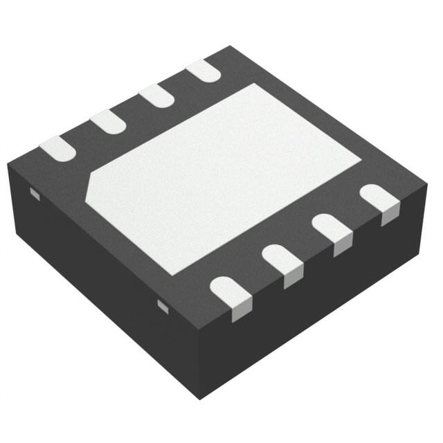
3-mm × 3-mm VSON-8 packages
Automotive infotainment
Navigation systems
WiFi, WiMax modules
Telematics systems
Microprocessor power
3 Description
The TPS735-Q1 family of low-dropout (LDO), lowpower linear regulators offers excellent ac
performance with very low ground current. High
power-supply rejection ratio (PSRR), low noise, fast
start-up, and excellent line and load transient
responses are provided while consuming a very low
46 µA (typical) ground current.
The TPS735-Q1 family of devices is stable with
ceramic capacitors and uses an advanced BiCMOS
fabrication process to yield a typical dropout voltage
of 280 mV at 500-mA output. The TPS735-Q1 family
of devices uses a precision voltage reference and
feedback loop to achieve overall accuracy of 2%
(VOUT > 2.2 V) over all load, line, process, and
temperature variations. This family of devices is fully
specified from TA = –40°C to 125°C and is offered in
a low-profile, 3-mm × 3-mm VSON package.
Device Information(1)
PART NUMBER
TPS735-Q1
PACKAGE
VSON (8)
BODY SIZE (NOM)
3.00 mm × 3.00 mm
(1) For all available packages, see the orderable addendum at
the end of the datasheet.
Typical Application
Optional input capacitor, CIN,
to improve source
impedance, noise, and PSRR.
VIN
IN
OUT
VOUT
TPS735-Q1
EN
VEN
GND
NR
2.2 µF
Ceramic
Optional bypass capacitor, CNR,
to reduce output noise
and increase PSRR.
1
An IMPORTANT NOTICE at the end of this data sheet addresses availability, warranty, changes, use in safety-critical applications,
intellectual property matters and other important disclaimers. PRODUCTION DATA.
�TPS735-Q1
SBVS252B – OCTOBER 2014 – REVISED FEBRUARY 2019
www.ti.com
Table of Contents
1
2
3
4
5
6
7
Features ..................................................................
Applications ...........................................................
Description .............................................................
Revision History.....................................................
Pin Configuration and Functions .........................
Specifications.........................................................
1
1
1
2
3
4
6.1
6.2
6.3
6.4
6.5
6.6
4
4
4
4
5
6
Absolute Maximum Ratings ......................................
ESD Ratings..............................................................
Recommended Operating Conditions.......................
Thermal Information ..................................................
Electrical Characteristics...........................................
Typical Characteristics ..............................................
Detailed Description .............................................. 8
7.1
7.2
7.3
7.4
Overview ................................................................... 8
Functional Block Diagram ......................................... 8
Feature Description................................................... 9
Device Functional Modes........................................ 10
8
Application and Implementation ........................ 11
8.1 Application Information............................................ 11
8.2 Typical Application .................................................. 11
9 Power Supply Recommendations...................... 14
10 Layout................................................................... 14
10.1 Layout Guidelines ................................................. 14
10.2 Layout Example .................................................... 17
11 Device and Documentation Support ................. 18
11.1
11.2
11.3
11.4
11.5
11.6
11.7
Device Support......................................................
Documentation Support ........................................
Receiving Notification of Documentation Updates
Community Resources..........................................
Trademarks ...........................................................
Electrostatic Discharge Caution ............................
Glossary ................................................................
18
18
18
18
18
18
18
12 Mechanical, Packaging, and Orderable
Information ........................................................... 19
4 Revision History
Changes from Revision A (January 2015) to Revision B
Page
•
Added title to first page figure ................................................................................................................................................ 1
•
Changed time scale from 10 ms to 10 µs in TPS73525-Q1 Turn-On Response (VIN = VEN) figure ................................... 13
•
Changed time scale from 10 ms to 10 µs in TPS73525-Q1 Turn-On Response Using EN figure ...................................... 13
Changes from Original (October 2014) to Revision A
•
2
Page
Made changes to product preview document......................................................................................................................... 1
Submit Documentation Feedback
Copyright © 2014–2019, Texas Instruments Incorporated
Product Folder Links: TPS735-Q1
�TPS735-Q1
www.ti.com
SBVS252B – OCTOBER 2014 – REVISED FEBRUARY 2019
5 Pin Configuration and Functions
OUT
1
NC
2
NR/FB
3
GND
4
Exposed
Thermal Pad
DRB Package
8-Pin VSON With Exposed Thermal Pad
Top View
8 IN
7 NC
6 NC
5 EN
NC = No internal connection.
Pin Functions
PIN
NAME
NO.
I/O
DESCRIPTION
EN
5
I
Driving the enable pin (EN) high turns on the regulator. Driving this pin low puts the regulator into shutdown
mode. The EN pin can be connected to the IN pin if not used.
FB
3
I
This pin is only available for the adjustable version. The FB pin is the input to the control-loop error amplifier,
and is used to set the output voltage of the device.
GND
4
—
IN
8
I
NC
2, 6, 7
—
Not internally connected
NR
3
—
This pin is only available for the fixed voltage versions. Connecting an external capacitor to this pin
bypasses noise generated by the internal band gap and allows the output noise to be reduced to very low
levels. The maximum recommended capacitor is 0.01 µF.
OUT
1
O
This pin is the output of the regulator. A small 2-µF ceramic capacitor is required from this pin to ground to
assure stability.
—
The pad must be tied to the GND pin.
Exposed thermal
pad
Ground
Input supply
Submit Documentation Feedback
Copyright © 2014–2019, Texas Instruments Incorporated
Product Folder Links: TPS735-Q1
3
�TPS735-Q1
SBVS252B – OCTOBER 2014 – REVISED FEBRUARY 2019
www.ti.com
6 Specifications
6.1 Absolute Maximum Ratings
At –40°C ≤ TJ and TA ≤ 125°C (unless otherwise noted). All voltages are with respect to GND. (1)
Voltage
MIN
MAX
UNIT
VIN
–0.3
7
V
VEN
–0.3
VIN + 0.3
V
VFB
–0.3
1.6
V
VOUT
–0.3
VIN + 0.3
V
Current
IOUT
Continuous total power dissipation
Continuous, PD(tot)
Internally limited
A
See the Power Dissipation section
Operating junction temperature, TJ
–40
150
°C
Storage temperature, Tstg
–55
150
°C
(1)
Stresses beyond those listed as absolute maximum ratings may cause permanent damage to the device. These are stress ratings only,
and functional operation of the device at these or any other conditions beyond those indicated as recommended operating conditions is
not implied. Exposure to absolute-maximum-rated conditions for extended periods may affect device reliability.
6.2 ESD Ratings
VALUE
Human body model (HBM), per AEC Q100-002
V(ESD)
(1)
Electrostatic discharge
Charged device model (CDM), per
AEC Q100-011
(1)
UNIT
±2000
Corner pins (1, 4, 5, and 8)
±750
Other pins
±500
V
AEC Q100-002 indicates HBM stressing is done in accordance with the ANSI/ESDA/JEDEC JS-001 specification.
6.3 Recommended Operating Conditions
over operating free-air temperature range (unless otherwise noted)
MIN
MAX
VIN
Input voltage
2.7
6.5
VOUT
Output voltage
VFB
6
IOUT
Output current (1)
0
500
mA
TA
Operating free-air temperature
–40
125
°C
(1)
UNIT
V
V
When operating at TJ near 125°C, IOUT(min) is 500 µA.
6.4 Thermal Information
TPS735-Q1
THERMAL METRIC
(1)
DRB (VSON)
UNIT
8 PINS
RθJA
Junction-to-ambient thermal resistance
54.1
°C/W
RθJC(top)
Junction-to-case (top) thermal resistance
71.0
°C/W
RθJB
Junction-to-board thermal resistance
28.4
°C/W
ψJT
Junction-to-top characterization parameter
2.3
°C/W
ψJB
Junction-to-board characterization parameter
28.5
°C/W
RθJC(bot)
Junction-to-case (bottom) thermal resistance
9.7
°C/W
(1)
4
For more information about traditional and new thermal metrics, see the Semiconductor and IC Package Thermal Metrics application
report.
Submit Documentation Feedback
Copyright © 2014–2019, Texas Instruments Incorporated
Product Folder Links: TPS735-Q1
�TPS735-Q1
www.ti.com
SBVS252B – OCTOBER 2014 – REVISED FEBRUARY 2019
6.5 Electrical Characteristics
Over operating temperature range (–40°C ≤ TJ, TA ≤ 125°C), VIN = VOUTnom + 0.5 V or 2.7 V (whichever is greater), IOUT =
1 mA, VEN = VIN, COUT = 2.2 μF, and CNR = 0.01 μF, unless otherwise noted.
For the adjustable version (TPS73501-Q1), VOUT = 3 V. Typical values are at TA = 25°C.
PARAMETER
TEST CONDITIONS
(1)
VIN
Input voltage
VFB
Internal reference (TPS73501-Q1)
VOUT
Output voltage range
(TPS73501-Q1)
1.196
6
V
±1%
2%
–3%
±1%
3%
ΔVOUT(ΔIOUT)
Load regulation
500 µA ≤ IOUT ≤ 500 mA
VDO
Dropout voltage (2)
(VIN = VOUTnom – 0.1 V)
IOUT = 500 mA
ILIM
Output current limit
VOUT = 0.9 × VOUTnom, VIN = VOUTnom + 0.9 V,
VIN ≥ 2.7 V
IGND
Ground pin current
10 mA ≤ IOUT ≤ 500 mA
ISHDN
Shutdown current
VEN ≤ 0 V
IFB
Feedback pin current
(TPS73501-Q1)
VOUTnom = 1.2 V
Power-supply rejection ratio
VIN = 3.85 V, VOUT = 2.85 V,
CNR = 0.01 µF,
IOUT = 100 mA
BW = 10 Hz to
100 kHz, VOUT = 2.8 V
800
UNIT
0.02
%/V
0.005
%/mA
280
500
mV
1170
1900
mA
45
65
μA
0.15
1
μA
0.5
μA
–0.5
f = 100 Hz
60
dB
f = 1k Hz
68
dB
f = 10 kHz
41
dB
f = 100 kHz
21
dB
CNR = 0.01 μF
11 × VOUT
μVRMS
CNR = none
95 × VOUT
μVRMS
CNR = none
45
μs
CNR = 0.001 μF
45
μs
CNR = 0.01 μF
50
μs
CNR = 0.047 μF
50
μs
VEN(HI)
Enable high (enabled)
VEN(LO)
Enable low (shutdown)
IEN(HI)
Enable pin current, enabled
Tsd
Thermal shutdown temperature
UVLO
Undervoltage lockout
VIN rising
Vhys
Hysteresis
VIN falling
(1)
(2)
V
–2%
VOUTnom + 0.5 V ≤ VIN ≤ 6.5 V
Startup time
V
1.220
VOUT ≤ 2.2 V
Line regulation (1)
tSTR
6.5
1.208
VOUT > 2.2 V
ΔVOUT(ΔVIN)
Output noise voltage
MAX
VFB
1 mA ≤ IOUT ≤ 500 mA,
VOUT + 0.5 V ≤ VIN < 6.5 V
Vn
TYP
2.7
TJ = 25°C
DC output accuracy (1)
PSRR
MIN
1.2
V
VEN = VIN = 6.5 V
0.03
Shutdown, temperature increasing
165
Reset, temperature decreasing
145
1.9
2.2
0.4
V
1
μA
°C
°C
2.65
70
V
mV
Minimum VIN = VOUT + VDO or 2.7 V, whichever is greater.
VDO is not measured for this family of devices with VOUTnom < 2.8 V because the minimum VIN = 2.7 V.
Submit Documentation Feedback
Copyright © 2014–2019, Texas Instruments Incorporated
Product Folder Links: TPS735-Q1
5
�TPS735-Q1
SBVS252B – OCTOBER 2014 – REVISED FEBRUARY 2019
www.ti.com
6.6 Typical Characteristics
0.5
0.5
0.4
0.4
0.3
0.2
0.1
0
-0.1
TJ = 125°C
TJ = 85°C
TJ = 25°C
TJ = 0°C
TJ = –40°C
-0.2
-0.3
-0.4
-0.5
3
3.5
4
4.5
5
5.5
6
Change in Output Voltage (%)
Change in Output Voltage (%)
Over operating temperature range (–40°C ≤ TJ, TA ≤ 125°C), VIN = VOUTnom + 0.5 V or 2.7 V (whichever is greater), IOUT =
1 mA, VEN = VIN, COUT = 2.2 μF, and CNR = 0.01 μF, unless otherwise noted. TA = 25°C, unless otherwise noted.
TJ = 125°C
TJ = 85°C
TJ = 25°C
TJ = 0°C
TJ = –40°C
0.3
0.2
0.1
0
-0.1
-0.2
-0.3
-0.4
-0.5
3
6.5
3.5
4
2.53
TJ = –40°C
2.83
2.82
2.81
2.8
2.79
2.78
2.77
6.5
2.52
2.51
2.5
2.49
2.48
2.47
2.76
2.46
2.75
2.45
2.74
0
50
100 150 200 250 300 350 400 450 500
0
50
100 150 200 250 300 350 400 450 500
Load (mA)
Load (mA)
The y-axis range is ±2% of 2.8 V
The y-axis range is ±2% of 2.5 V
Figure 3. TPS73501-Q1 Load Regulation
Figure 4. TPS73525-Q1 Load Regulation
500
60
VIN = 6.5 V
VIN = 5 V
VIN = 3.3 V
50
40
30
TJ = 125°C
TJ = 85°C
TJ = 25°C
TJ = 0°C
TJ = –40°C
20
10
0
0
50
100 150 200 250 300 350 400 450 500
Current on the GND Pin (nA)
450
Current on the GND Pin (mA)
6
TJ = 125°C
TJ = 85°C
TJ = 25°C
TJ = 0°C
TJ = –40°C
2.54
Output Voltage (V)
Output Voltage (V)
2.55
TJ = 125°C
TJ = 85°C
2.84
5.5
Figure 2. TPS73525-Q1 Line Regulation
Figure 1. TPS73501-Q1 Line Regulation
2.85
5
IOUT = 100 mA
IOUT = 100 mA
2.86
4.5
Input Voltage (V)
Input Voltage (V)
400
350
300
250
200
150
100
50
0
-40 -25 -10
5
20
35
50
65
80
95
110 125
Junction Temperature (°C)
Output Current (mA)
VEN = 0.4 V
Figure 5. TPS73525-Q1 Ground Pin Current vs
Output Current
6
Figure 6. TPS73525-Q1 Ground Pin Current (Disable) vs
Temperature
Submit Documentation Feedback
Copyright © 2014–2019, Texas Instruments Incorporated
Product Folder Links: TPS735-Q1
�TPS735-Q1
www.ti.com
SBVS252B – OCTOBER 2014 – REVISED FEBRUARY 2019
Typical Characteristics (continued)
Over operating temperature range (–40°C ≤ TJ, TA ≤ 125°C), VIN = VOUTnom + 0.5 V or 2.7 V (whichever is greater), IOUT =
1 mA, VEN = VIN, COUT = 2.2 μF, and CNR = 0.01 μF, unless otherwise noted. TA = 25°C, unless otherwise noted.
400
300
250
80
70
PSRR (dB)
350
Dropout Voltage (mV)
90
TJ = 125°C
TJ = 85°C
TJ = 25°C
TJ = 0°C
TJ = –40°C
200
150
60
50
40
IOUT = 1 mA
IOUT = 100 mA
IOUT = 200 mA
IOUT = 250 mA
IOUT = 500 mA
30
100
20
50
10
0
0
0
50
10
100 150 200 250 300 350 400 450 500
100
10k
1k
100k
1M
10M
Frequency (Hz)
Figure 7. TPS73501-Q1 Dropout Voltage vs Output Current
Figure 8. Power-Supply Ripple Rejection vs Frequency
(VIN – VOUT = 1 V)
90
90
80
80
70
70
60
60
PSRR (dB)
PSRR (dB)
Output Current (mA)
50
40
IOUT = 1 mA
IOUT = 100 mA
IOUT = 200 mA
IOUT = 250 mA
IOUT = 500 mA
30
20
10
40
30
IOUT = 1 mA
IOUT = 100 mA
IOUT = 200 mA
IOUT = 250 mA
IOUT = 500 mA
20
10
0
0
10
100
10k
1k
100k
1M
10M
10
100
10k
1k
100k
1M
10M
Frequency (Hz)
Frequency (Hz)
Figure 9. Power-Supply Ripple Rejection vs Frequency
(VIN – VOUT = 0.5 V)
Figure 10. Power-Supply Ripple Rejection vs Frequency
(VIN – VOUT = 0.3 V)
140
30
120
25
Total Noise (mVRMS)
Total Noise (mVRMS)
50
100
80
60
40
20
15
10
5
20
0
0
0.01
0.1
10
1
5
0
10
15
20
25
Output Capacitance (mF)
Capacitance on the NR Pin (nF)
CNR = 0.01 µF, IOUT = 1 mA
Figure 11. TPS73525-Q1 RMS Noise vs CNR
Figure 12. TPS73525-Q1 RMS Noise vs COUT
Submit Documentation Feedback
Copyright © 2014–2019, Texas Instruments Incorporated
Product Folder Links: TPS735-Q1
7
�TPS735-Q1
SBVS252B – OCTOBER 2014 – REVISED FEBRUARY 2019
www.ti.com
7 Detailed Description
7.1 Overview
The TPS735-Q1 family of low dropout (LDO) regulators combines the high performance required by many radio
frequency (RF) and precision analog applications with ultra-low current consumption. High PSRR is provided by
a high-gain, high-bandwidth error loop with good supply rejection and very low headroom (VIN – VOUT). Fixed
voltage versions provide a noise reduction pin to bypass noise generated by the band-gap reference and to
improve PSRR. A quick-start circuit fast-charges this capacitor at startup. The combination of high performance
and low ground current also make the TPS735-Q1 family of devices an excellent choice for portable applications.
All versions have thermal and overcurrent protection and are fully specified from –40°C ≤ TJ, TA ≤ 125°C.
7.2 Functional Block Diagram
IN
OUT
400
2 mA
Current
Limit
Overshoot
Detect
Thermal
Shutdown
EN
UVLO
Quickstart
1.208-V
Bandgap(1)
NR
500 k
GND
NOTE: Fixed voltage versions between 1 V to 1.2 V have a 1-V band-gap circuit instead of a 1.208-V band-gap circuit.
Figure 13. Fixed Voltage Versions
IN
OUT
400
3.3 M
Current
Limit
Overshoot
Detect
Thermal
Shutdown
EN
UVLO
1.208-V
Bandgap
FB
500 k
GND
Figure 14. Adjustable Voltage Versions
8
Submit Documentation Feedback
Copyright © 2014–2019, Texas Instruments Incorporated
Product Folder Links: TPS735-Q1
�TPS735-Q1
www.ti.com
SBVS252B – OCTOBER 2014 – REVISED FEBRUARY 2019
7.3 Feature Description
7.3.1 Internal Current-Limit
The TPS735-Q1 internal current-limit helps protect the regulator during fault conditions. During current-limit, the
output sources a fixed amount of current that is largely independent of the output voltage. For reliable operation,
do not operate the device in current-limit for extended periods of time.
The PMOS pass element in the TPS735-Q1 family of devices has a built-in body diode that conducts current
when the voltage at the OUT pin exceeds the voltage at the IN pin. This current is not limited, so if extended
reverse voltage operation is anticipated, external limiting can be appropriate.
7.3.2 Shutdown
The enable pin (EN) is active high and is compatible with standard and low-voltage TTL-CMOS levels. When
shutdown capability is not required, the EN pin can be connected to the IN pin.
7.3.3 Dropout Voltage
The TPS735-Q1 family of devices uses a PMOS pass transistor to achieve low dropout. When (VIN – VOUT) is
less than the dropout voltage (VDO), the PMOS pass device is in the linear region of operation and the input-tooutput resistance (R(IN/OUT)) of the PMOS pass element. VDO scales with the output current because the PMOS
device behaves like a resistor in dropout.
As with any linear regulator, PSRR and transient response are degraded when (VIN – VOUT) approaches dropout.
This effect is shown in the Typical Characteristics section (see Figure 8 through Figure 10).
7.3.4 Startup and Noise Reduction Capacitor
Fixed voltage versions of the TPS735-Q1 family of devices use a quick-start circuit to fast-charge the noise
reduction capacitor, CNR, if present (see the Functional Block Diagram section). This architecture allows the
combination of very-low output noise and fast startup times. The NR pin is high impedance so a low-leakage CNR
capacitor must be used. Most ceramic capacitors are appropriate in this configuration. A high-quality, COG-type
(NPO) dielectric ceramic capacitor is recommended for CNR when used in environments where abrupt changes in
temperature can occur.
Note that for fastest start-up, apply VIN first, then drive the enable pin (EN) high. If the EN pin is tied to the IN pin,
start-up is somewhat slower. Refer to the Typical Application section (see Figure 17 and Figure 18). The quickstart switch is closed for approximately 135 μs. To ensure that CNR is charged during the quick-start time, use a
capacitor with a value of no more than 0.01 μF.
7.3.5 Transient Response
As with any regulator, increasing the size of the output capacitor reduces overshoot and undershoot magnitude
but increases the transient response duration. In the adjustable version, adding CFB between the OUT and FB
pins improves stability and transient response performance. The transient response of the TPS735-Q1 family of
devices is enhanced by an active pulldown that engages when the output overshoots by approximately 5% or
more when the device is enabled. When enabled, the pull-down device behaves like a 400-Ω resistor to ground.
7.3.6 Undervoltage Lockout (UVLO)
The TPS735-Q1 family of devices uses an undervoltage lockout circuit to keep the output shut off until the
internal circuitry is operating properly. The UVLO circuit has a deglitch feature so that the UVLO typically ignores
undershoot transients on the input if the transients are less than 50 μs in duration.
7.3.7 Minimum Load
The TPS735-Q1 family of devices is stable and well-behaved with no output load. To meet the specified
accuracy, a minimum load of 500 μA is required. Below 500 μA and at junction temperatures near 125°C, the
output can drift up enough to cause the output pulldown to turn on. The output pulldown limits voltage drift to 5%
(typically) but ground current can increase by approximately 50 μA. In most applications, the junction does not
reach high temperatures at light loads because very little power is dissipated. Therefore, the specified ground
current is valid at no load in most applications.
Submit Documentation Feedback
Copyright © 2014–2019, Texas Instruments Incorporated
Product Folder Links: TPS735-Q1
9
�TPS735-Q1
SBVS252B – OCTOBER 2014 – REVISED FEBRUARY 2019
www.ti.com
7.4 Device Functional Modes
7.4.1 Normal Operation
The device regulates to the nominal output voltage under the following conditions:
•
The input voltage has previously exceeded the UVLO voltage and has not decreased below the UVLO
threshold minus Vhys.
The input voltage is greater than the nominal output voltage added to the dropout voltage.
The enable voltage has previously exceeded the enable rising threshold voltage and has not decreased
below the enable falling threshold.
The output current is less than the current limit.
The device junction temperature is less than the thermal shutdown temperature.
•
•
•
•
7.4.2 Dropout Operation
If the input voltage is lower than the nominal output voltage plus the specified dropout voltage, but all other
conditions are met for normal operation, the device operates in dropout mode. In this condition, the output
voltage is equal to the input voltage minus the dropout voltage. The transient performance of the device is
significantly degraded because the pass device is in a triode state and the LDO behaves like a resistor. Line or
load transients in dropout can result in large output voltage deviations.
7.4.3 Disabled
The device is disabled under the following conditions:
• The input voltage is less than the UVLO threshold minus Vhys, or has not yet exceeded the UVLO threshold.
• The enable voltage is less than the enable falling threshold voltage or has not yet exceeded the enable rising
threshold.
• The device junction temperature is greater than the thermal shutdown temperature.
Table 1 shows the conditions that lead to the different modes of operation.
Table 1. Device Functional Mode Comparison
PARAMETER
OPERATING MODE
VIN
VEN
IOUT
TJ
Normal mode
VIN > VOUTnom + VDO and VIN > UVLO
VEN > VEN(HI)
IOUT < ILIM
TJ < 165°C
Dropout mode
UVLO < VIN < VOUTnom + VDO
VEN > VEN(HI)
—
TJ < 165°C
VIN < UVLO – Vhys
VEN < VEN(LO)
—
TJ > 165°C
Disabled mode
(any true condition
disables the device)
10
Submit Documentation Feedback
Copyright © 2014–2019, Texas Instruments Incorporated
Product Folder Links: TPS735-Q1
�TPS735-Q1
www.ti.com
SBVS252B – OCTOBER 2014 – REVISED FEBRUARY 2019
8 Application and Implementation
NOTE
Information in the following applications sections is not part of the TI component
specification, and TI does not warrant its accuracy or completeness. TI’s customers are
responsible for determining suitability of components for their purposes. Customers should
validate and test their design implementation to confirm system functionality.
8.1 Application Information
The TPS735-Q1 family of automotive-qualified LDO regulators provides a design with an ultra-low noise, high
PSRR, low-dropout linear regulation with a very small ground current (46 µA, typical).
The devices are stable with ceramic capacitors, and have a dropout voltage of 280 mV at the full output rating of
500 mA. The features of the TPS735-Q1 family of devices enables the LDO regulators to be suitable for a wide
variety of applications, with minimal design complexity.
8.2 Typical Application
Figure 15 shows the basic circuit connections for fixed-voltage models. Figure 16 gives the connections for the
adjustable output version (TPS73501-Q1). Use the equation in Figure 16 to calculate the value of R1 and R2 for
any output voltage.
Optional input capacitor, CIN,
to improve source
impedance, noise, and PSRR.
VIN
IN
VOUT
OUT
TPS735-Q1
EN
GND
VEN
2.2 µF
Ceramic
NR
Optional bypass capacitor, CNR,
to reduce output noise
and increase PSRR.
Figure 15. Typical Application Circuit for Fixed Voltage Versions
Optional input capacitor, CIN,
to improve source
impedance, noise, and PSRR.
VIN
IN
VOUT(nom) =
(R1 + R2)
R2
VOUT
OUT
TPS73501-Q1
EN
GND
× 1.208 V
R1
FB
CFB
2.2 µF
Ceramic
R2
VEN
Figure 16. Typical Application Circuit for Adjustable Voltage Versions
Submit Documentation Feedback
Copyright © 2014–2019, Texas Instruments Incorporated
Product Folder Links: TPS735-Q1
11
�TPS735-Q1
SBVS252B – OCTOBER 2014 – REVISED FEBRUARY 2019
www.ti.com
Typical Application (continued)
8.2.1 Design Requirements
8.2.1.1 Input and Output Capacitor Requirements
Although an input capacitor is not required for stability, connecting a 0.1-μF to 1-μF low-equivalent seriesresistance (ESR) capacitor across the input supply near the regulator is good analog design practice. This
capacitor counteracts reactive input sources and improves transient response and ripple rejection. A higher-value
capacitor can be necessary if large, fast, rise-time load transients are anticipated or if the device is located
several inches from the power source. If source impedance is not sufficiently low, a 0.1-μF input capacitor can be
necessary to ensure stability.
The TPS735-Q1 family of devices is designed to be stable with standard ceramic output capacitors of values
2 μF or larger. X5R- and X7R-type capacitors are best because they have minimal variation in value and ESR
over temperature. Maximum ESR of the output capacitor is < 1 Ω and, therefore, the output capacitor type must
either be ceramic or conductive polymer electrolytic.
8.2.1.2 Feedback Capacitor Requirements (TPS73501-Q1 only)
The feedback capacitor (CFB), shown in Figure 16, is required for stability. For a parallel combination of R1 and
R2 equal to 250 kΩ, any value between 3 pF to 1 nF can be used. Fixed voltage versions have an internal 30-pF
feedback capacitor that is quick-charged at start-up. Larger value capacitors also improve noise slightly. The
TPS73501-Q1 device is stable in unity-gain configurations (the OUT pin is tied to the FB pin) without CFB.
8.2.2 Detailed Design Procedure
8.2.2.1 Output Noise
In most LDO regulators, the band gap is the dominant noise source. If a noise-reduction capacitor (CNR) is used
with the TPS735-Q1 family of devices, the band gap does not contribute significantly to noise. Instead, noise is
dominated by the output-resistor divider and the error-amplifier input. To minimize noise in a given application,
use a 0.01-μF noise reduction capacitor. For the adjustable version, smaller value resistors in the output resistor
divider reduce noise. A parallel combination that gives 2 μA of divider current has the same noise performance
as a fixed voltage version with a CNR. To further optimize noise, ESR of the output capacitor can be set to
approximately 0.2 Ω. This configuration maximizes phase margin in the control loop, reducing the total output
noise up to 10%. The maximum recommended capacitor is 0.01 µF.
Equation 1 calculates the approximate integrated output noise from 10 Hz to 100 kHz with a CNR value of
0.01 µF.
Vn (µVRMS) = 11 (µVRMS / V) × VOUT (V)
(1)
The TPS73501-Q1 adjustable version does not have the noise-reduction pin available, so ultra-low noise
operation is not possible. Noise can be minimized according to the previously listed recommendations.
12
Submit Documentation Feedback
Copyright © 2014–2019, Texas Instruments Incorporated
Product Folder Links: TPS735-Q1
�TPS735-Q1
www.ti.com
SBVS252B – OCTOBER 2014 – REVISED FEBRUARY 2019
Typical Application (continued)
8.2.3 Application Curves
3.5
3.5
3
3
2.5
2.5
2
2
Voltage (V)
Voltage (V)
At VIN = VOUTnom + 0.5 V or 2.7 V (whichever is greater), IOUT = 1 mA, VEN = VIN, COUT = 2.2 μF, CNR = 0.01 μF,
and TA = 25°C, unless otherwise noted.
1.5
1
0.5
1.5
1
0.5
VOUT, COUT = 10 mF
VOUT, COUT = 2.2 mF
VEN
0
VOUT, COUT = 10 mF
VOUT, COUT = 2.2 mF
VEN
0
-0.5
-0.5
10 μs/div
10 µs/div
Figure 17. TPS73525-Q1 Turn-On Response (VIN = VEN)
Figure 18. TPS73525-Q1 Turn-On Response Using EN
7
COUT = 470 mF OSCON
VOUT
6
200 mV/div
VIN = VEN
COUT = 10 mF
200 mV/div
Voltage (V)
5
4
COUT = 2.2 mF
200 mV/div
3
2
VOUT
1
500 mA
0
500 mA/div
IOUT
1 mA
-1
10 ms/div
10 ms/div
VIN = 3 V
RL = 5 Ω
Figure 20. TPS73525-Q1 Load Transient Response
Figure 19. TPS73525-Q1 Power-Up and Power-Down
(VIN = VEN)
COUT = 470 mF OSCON
50 mV/div
COUT = 10VmOUT
F
50 mV/div
COUT = 2.2 mF
50 mV/div
4V
VOUT
VIN
0.5 V/div
3V
10 ms/div
Figure 21. TPS73525-Q1 Line Transient Response
Submit Documentation Feedback
Copyright © 2014–2019, Texas Instruments Incorporated
Product Folder Links: TPS735-Q1
13
�TPS735-Q1
SBVS252B – OCTOBER 2014 – REVISED FEBRUARY 2019
www.ti.com
9 Power Supply Recommendations
The device is designed to operate from an input voltage supply range between 2.7 V and 6.5 V. The input
voltage range must provide adequate headroom in order for the device to have a regulated output. This input
supply must be well regulated. If the input supply is noisy, additional input capacitors with low ESR can help
improve output noise.
10 Layout
10.1 Layout Guidelines
For best overall performance, place all circuit components on the same side of the circuit board and as near as
practical to the respective LDO pin connections. Place ground return connections to the input and output
capacitor, and to the LDO ground pin as close to each other as possible, connected by a wide, component-side,
copper surface. The use of vias and long traces to create LDO component connections is strongly discouraged
and negatively affects system performance. This grounding and layout scheme minimizes inductive parasitics,
and thereby reduces load-current transients, minimizes noise, and increases circuit stability. A ground reference
plane is also recommended and is either embedded in the printed circuit board (PCB) itself or located on the
bottom side of the PCB opposite the components. This reference plane serves to assure accuracy of the output
voltage, shields the LDO from noise, and behaves similar to a thermal plane to spread (or sink) heat from the
LDO device when connected to the PowerPAD™. In most applications, this ground plane is necessary to meet
thermal requirements.
10.1.1 Board Layout Recommendations to Improve PSRR and Noise Performance
To improve ac performance (such as PSRR, output noise, and transient response), designing the board with
separate ground planes for VIN and VOUT is recommended, with each ground plane connected only at the GND
pin of the device. In addition, the ground connection for the bypass capacitor must connect directly to the GND
pin of the device.
10.1.2 Thermal Protection
Thermal protection disables the output when the junction temperature rises to approximately 165°C, allowing the
device to cool. When the junction temperature cools to approximately 145°C, the output circuitry is again
enabled. Depending on power dissipation, thermal resistance, and ambient temperature, the thermal protection
circuit can cycle on and off. This cycling limits the dissipation of the regulator, protecting it from damage as a
result of overheating.
Any tendency to activate the thermal protection circuit indicates excessive power dissipation or an inadequate
heatsink. For reliable operation, limit junction temperature to 125°C maximum. To estimate the thermal margin in
a complete design (including heatsink), increase the ambient temperature until the thermal protection is triggered;
use worst-case loads and signal conditions. For good reliability, trigger thermal protection at least 40°C above
the maximum expected ambient condition of a particular application. This configuration produces a worst-case
junction temperature of 125°C at the highest expected ambient temperature and worst-case load.
The internal protection circuitry of the TPS735-Q1 family of devices is designed to protect against overload
conditions. This protection circuitry is not intended to replace proper heatsinking. Continuously running the
TPS735-Q1 family of devices into thermal shutdown degrades device reliability.
10.1.3 Package Mounting
Solder pad footprint recommendations for the TPS735-Q1 family of devices are available from the Texas
Instruments web site at www.ti.com.
10.1.4 Power Dissipation
The ability to remove heat from the die is different for each package type, presenting different considerations in
the PCB layout. The PCB area around the device that is free of other components moves the heat from the
device to the ambient air. Performance data for JEDEC low- and high-K boards are given in the Thermal
Information table. Using heavier copper increases the effectiveness in removing heat from the device. The
addition of plated through-holes to heat-dissipating layers also improves the heatsink effectiveness.
14
Submit Documentation Feedback
Copyright © 2014–2019, Texas Instruments Incorporated
Product Folder Links: TPS735-Q1
�TPS735-Q1
www.ti.com
SBVS252B – OCTOBER 2014 – REVISED FEBRUARY 2019
Layout Guidelines (continued)
Power dissipation depends on input voltage and load conditions. Power dissipation is equal to the product of the
output current and the voltage drop across the output pass element, as shown in Equation 2.
PD = (VIN – VOUT) × IOUT
(2)
NOTE
When the device is used in a condition of high input and low output voltages, PD can
exceed the junction temperature rating even when the ambient temperature is at room
temperature.
Equation 3 is an example calculation for the power dissipation (PD) of the DRB package.
PD = (6.5 V – 1.2 V) × 500 mA = 2.65 W
(3)
Power dissipation can be minimized and greater efficiency can be achieved by using the lowest possible input
voltage necessary to achieve the required output performance.
On the DRB package, the primary conduction path for heat is through the exposed thermal pad to the PCB. The
pad can be connected to ground or left floating; however, the pad must be attached to an appropriate amount of
copper PCB area to ensure the device does not overheat. The maximum allowable junction-to-ambient thermal
resistance depends on the maximum ambient temperature, maximum device junction temperature, and power
dissipation of the device. Use Equation 4 to calculate the maximum junction-to-ambient thermal resistance.
125qC TA
RTJA
PD
(4)
Submit Documentation Feedback
Copyright © 2014–2019, Texas Instruments Incorporated
Product Folder Links: TPS735-Q1
15
�TPS735-Q1
SBVS252B – OCTOBER 2014 – REVISED FEBRUARY 2019
www.ti.com
Layout Guidelines (continued)
Knowing the maximum RθJA, the minimum amount of PCB copper area needed for appropriate heatsinking can
be estimated using Figure 22.
Junction-to-Ambient Thermal
Resistance (°C/W)
160
140
120
100
80
60
40
20
0
0
1
2
3
4
5
6
7
8
9
10
2
Board Copper Area (in )
NOTE: The RθJA value at a board size of 9 in2 (that is, 3 in × 3 in) is a JEDEC standard.
Figure 22. RθJA vs Board Size
Figure 22 shows the variation of RθJA as a function of copper area in the board that is connected to the thermal
pad. Figure 22 is intended only as a guideline to demonstrate the effects of heat spreading in the ground plane
and is not to be used to calculate actual thermal performance.
NOTE
When the device is mounted on an application PCB, TI strongly recommends using ΨJT
and ΨJB, as explained in the Estimating Junction Temperature section.
10.1.5 Estimating Junction Temperature
Using the thermal metrics ΨJT and ΨJB, as shown in the Thermal Information table, the junction temperature can
be estimated with the corresponding formulas (given in Equation 5).
< JT : TJ TT < JT u PD
< JB : TJ
TB
< JB u PD
where:
•
•
•
PD is the power dissipation calculated with Equation 2,
TT is the temperature at the center-top of the device package, and
TB is the PCB temperature measured 1 mm away from the device package on the PCB surface (as shown in
Figure 23).
(5)
TT on top
of IC
TB on PCB
surface
1 mm
Figure 23. Measuring Points for TT and TB
16
Submit Documentation Feedback
Copyright © 2014–2019, Texas Instruments Incorporated
Product Folder Links: TPS735-Q1
�TPS735-Q1
www.ti.com
SBVS252B – OCTOBER 2014 – REVISED FEBRUARY 2019
Layout Guidelines (continued)
NOTE
Both TT and TB can be measured on actual application boards using an infrared
thermometer.
For more information about measuring TT and TB, see the application note, Using New Thermal Metrics,
SBVA025.
According to Figure 24, the thermal metrics (ΨJT and ΨJB) have very little dependency on copper area. Using ΨJT
or ΨJB with Equation 5 is a good way to estimate TJ by simply measuring TT or TB on an application board.
35
JB
JT
25
20
15
JT
and
JB
(°C/W)
30
10
5
0
0
1
2
3
4
5
6
7
8
9
10
Board Copper Area (in2)
Figure 24. ΨJT and ΨJB vs Board Size
10.2 Layout Example
Input GND
Plane
VOUT
CIN(1)
COUT(1)
OUT
1
NC
2
NR/FB
3
GND
4
CNR(1)
Thermal
Pad
8
IN
7
NC
6
NC
5
EN
VIN
Output GND
Plane
(1)
CIN and COUT are 0603 capacitors and CNR is a 0402 capacitor. The footprint is shown to scale with package size.
Figure 25. TPS735-Q1 Fixed Version Layout Reference Diagram
Submit Documentation Feedback
Copyright © 2014–2019, Texas Instruments Incorporated
Product Folder Links: TPS735-Q1
17
�TPS735-Q1
SBVS252B – OCTOBER 2014 – REVISED FEBRUARY 2019
www.ti.com
11 Device and Documentation Support
11.1 Device Support
11.1.1 Device Nomenclature
Table 2. Device Nomenclature (1)
PRODUCT
TPS735xx(x)yyyz
(1)
VOUT
XX(X) is the nominal output voltage. For output voltages with a resolution of 100 mV, two
digits are used in the ordering number; otherwise, three digits are used (for example, 33 =
3.3 V; 125 = 1.25 V).
YYY is the package designator.
Z is the tape and reel quantity (R = 3000, T = 250).
01 is the adjustable version.
For the most current package and ordering information see the Package Option Addendum at the end of this document, or see the TI
web site at www.ti.com.
11.2 Documentation Support
11.2.1 Related Documentation
For related documentation see the following:
• Texas Instruments, Semiconductor and IC package thermal metrics application report
• Texas Instruments, TPS735xxEVM-276 user's guide
• Texas Instruments, Using new thermal metrics application report
11.3 Receiving Notification of Documentation Updates
To receive notification of documentation updates, navigate to the device product folder on ti.com. In the upper
right corner, click on Alert me to register and receive a weekly digest of any product information that has
changed. For change details, review the revision history included in any revised document.
11.4 Community Resources
The following links connect to TI community resources. Linked contents are provided "AS IS" by the respective
contributors. They do not constitute TI specifications and do not necessarily reflect TI's views; see TI's Terms of
Use.
TI E2E™ Online Community TI's Engineer-to-Engineer (E2E) Community. Created to foster collaboration
among engineers. At e2e.ti.com, you can ask questions, share knowledge, explore ideas and help
solve problems with fellow engineers.
Design Support TI's Design Support Quickly find helpful E2E forums along with design support tools and
contact information for technical support.
11.5 Trademarks
E2E is a trademark of Texas Instruments.
PowerPAD is a trademark of Texas Instruments, Inc.
All other trademarks are the property of their respective owners.
11.6 Electrostatic Discharge Caution
This integrated circuit can be damaged by ESD. Texas Instruments recommends that all integrated circuits be handled with
appropriate precautions. Failure to observe proper handling and installation procedures can cause damage.
ESD damage can range from subtle performance degradation to complete device failure. Precision integrated circuits may be more
susceptible to damage because very small parametric changes could cause the device not to meet its published specifications.
11.7 Glossary
SLYZ022 — TI Glossary.
This glossary lists and explains terms, acronyms, and definitions.
18
Submit Documentation Feedback
Copyright © 2014–2019, Texas Instruments Incorporated
Product Folder Links: TPS735-Q1
�TPS735-Q1
www.ti.com
SBVS252B – OCTOBER 2014 – REVISED FEBRUARY 2019
12 Mechanical, Packaging, and Orderable Information
The following pages include mechanical, packaging, and orderable information. This information is the most
current data available for the designated family of devices. This data is subject to change without notice and
revision of this document. For browser-based versions of this data sheet, refer to the left-hand navigation.
Submit Documentation Feedback
Copyright © 2014–2019, Texas Instruments Incorporated
Product Folder Links: TPS735-Q1
19
�TPS735-Q1
SBVS252B – OCTOBER 2014 – REVISED FEBRUARY 2019
www.ti.com
PACKAGE OUTLINE
DRB0008B
VSON - 1 mm max height
SCALE 4.000
PLASTIC SMALL OUTLINE - NO LEAD
3.1
2.9
A
B
PIN 1 INDEX AREA
3.1
2.9
C
1 MAX
SEATING PLANE
0.05
0.00
0.08 C
EXPOSED
THERMAL PAD
1.65 0.05
(0.2) TYP
4
5
2X
1.95
2.4 0.05
8
1
6X 0.65
8X
PIN 1 ID
(OPTIONAL)
8X
0.5
0.3
0.35
0.25
0.1
0.05
C A B
C
4218876/A 12/2017
NOTES:
1. All linear dimensions are in millimeters. Any dimensions in parenthesis are for reference only. Dimensioning and tolerancing
per ASME Y14.5M.
2. This drawing is subject to change without notice.
3. The package thermal pad must be soldered to the printed circuit board for thermal and mechanical performance.
www.ti.com
20
Submit Documentation Feedback
Copyright © 2014–2019, Texas Instruments Incorporated
Product Folder Links: TPS735-Q1
�TPS735-Q1
www.ti.com
SBVS252B – OCTOBER 2014 – REVISED FEBRUARY 2019
EXAMPLE BOARD LAYOUT
DRB0008B
VSON - 1 mm max height
PLASTIC SMALL OUTLINE - NO LEAD
(1.65)
SYMM
8X (0.6)
1
8
8X (0.3)
(2.4)
(0.95)
6X (0.65)
4
5
(R0.05) TYP
(0.575)
( 0.2) VIA
TYP
(2.8)
LAND PATTERN EXAMPLE
SCALE:20X
0.07 MIN
ALL AROUND
0.07 MAX
ALL AROUND
SOLDER MASK
OPENING
METAL
METAL UNDER
SOLDER MASK
NON SOLDER MASK
DEFINED
(PREFERRED)
SOLDER MASK
OPENING
SOLDER MASK
DEFINED
SOLDER MASK DETAILS
4218876/A 12/2017
NOTES: (continued)
4. This package is designed to be soldered to a thermal pad on the board. For more information, see Texas Instruments literature
number SLUA271 (www.ti.com/lit/slua271).
5. Vias are optional depending on application, refer to device data sheet. If any vias are implemented, refer to their locations shown
on this view. It is recommended that vias under paste be filled, plugged or tented.
www.ti.com
Submit Documentation Feedback
Copyright © 2014–2019, Texas Instruments Incorporated
Product Folder Links: TPS735-Q1
21
�TPS735-Q1
SBVS252B – OCTOBER 2014 – REVISED FEBRUARY 2019
www.ti.com
EXAMPLE STENCIL DESIGN
DRB0008B
VSON - 1 mm max height
PLASTIC SMALL OUTLINE - NO LEAD
SYMM
8X (0.6)
METAL
TYP
1
8
8X (0.3)
(0.63)
SYMM
(1.06)
6X (0.65)
5
4
(R0.05) TYP
(1.47)
(2.8)
SOLDER PASTE EXAMPLE
BASED ON 0.125 mm THICK STENCIL
EXPOSED PAD
81% PRINTED SOLDER COVERAGE BY AREA
SCALE:25X
4218876/A 12/2017
NOTES: (continued)
6. Laser cutting apertures with trapezoidal walls and rounded corners may offer better paste release. IPC-7525 may have alternate
design recommendations.
www.ti.com
22
Submit Documentation Feedback
Copyright © 2014–2019, Texas Instruments Incorporated
Product Folder Links: TPS735-Q1
�PACKAGE OPTION ADDENDUM
www.ti.com
10-Dec-2020
PACKAGING INFORMATION
Orderable Device
Status
(1)
Package Type Package Pins Package
Drawing
Qty
Eco Plan
(2)
Lead finish/
Ball material
MSL Peak Temp
Op Temp (°C)
Device Marking
(3)
(4/5)
(6)
TPS73501QDRBRQ1
ACTIVE
SON
DRB
8
3000
RoHS & Green
NIPDAU
Level-3-260C-168 HR
-40 to 125
501DRB
TPS73512QDRBRQ1
ACTIVE
SON
DRB
8
3000
RoHS & Green
NIPDAU
Level-3-260C-168 HR
-40 to 125
512DRB
TPS73515QDRBRQ1
ACTIVE
SON
DRB
8
3000
RoHS & Green
NIPDAU
Level-3-260C-168 HR
-40 to 125
515DRB
TPS73518QDRBRQ1
ACTIVE
SON
DRB
8
3000
RoHS & Green
NIPDAU
Level-3-260C-168 HR
-40 to 125
518DRB
TPS73525QDRBRQ1
ACTIVE
SON
DRB
8
3000
RoHS & Green
NIPDAU
Level-3-260C-168 HR
-40 to 125
525DRB
TPS73527QDRBRQ1
ACTIVE
SON
DRB
8
3000
RoHS & Green
NIPDAU
Level-3-260C-168 HR
-40 to 125
527DRB
TPS73530QDRBRQ1
ACTIVE
SON
DRB
8
3000
RoHS & Green
NIPDAU
Level-3-260C-168 HR
-40 to 125
530DRB
TPS73533QDRBRQ1
ACTIVE
SON
DRB
8
3000
RoHS & Green
NIPDAU
Level-3-260C-168 HR
-40 to 125
533DRB
(1)
The marketing status values are defined as follows:
ACTIVE: Product device recommended for new designs.
LIFEBUY: TI has announced that the device will be discontinued, and a lifetime-buy period is in effect.
NRND: Not recommended for new designs. Device is in production to support existing customers, but TI does not recommend using this part in a new design.
PREVIEW: Device has been announced but is not in production. Samples may or may not be available.
OBSOLETE: TI has discontinued the production of the device.
(2)
RoHS: TI defines "RoHS" to mean semiconductor products that are compliant with the current EU RoHS requirements for all 10 RoHS substances, including the requirement that RoHS substance
do not exceed 0.1% by weight in homogeneous materials. Where designed to be soldered at high temperatures, "RoHS" products are suitable for use in specified lead-free processes. TI may
reference these types of products as "Pb-Free".
RoHS Exempt: TI defines "RoHS Exempt" to mean products that contain lead but are compliant with EU RoHS pursuant to a specific EU RoHS exemption.
Green: TI defines "Green" to mean the content of Chlorine (Cl) and Bromine (Br) based flame retardants meet JS709B low halogen requirements of


 工商网监
湘ICP备2023018690号
工商网监
湘ICP备2023018690号
