Product
Folder
Order
Now
Support &
Community
Tools &
Software
Technical
Documents
TPS7A47-Q1
SBVS118 – AUGUST 2017
TPS7A47-Q1 35-V, 1-A, 4.2-µVRMS, RF LDO Voltage Regulator
1 Features
2 Applications
•
•
•
•
•
•
1
•
•
•
•
•
•
•
•
•
•
Qualified for Automotive Applications
AEC-Q100 Qualified With the Following Results:
– Device Temperature Grade 1: –40°C to 125°C
Ambient Operating Temperature Range
– Device HBM ESD Classification Level 2
– Device CDM ESD Classification Level C4A
Input Voltage: 3 V to 35 V
Operating Junction Temperature: –40°C to
+145°C
Output Voltage Noise:
4.2 µVRMS (10 Hz–100 kHz)
Power-Supply Rejection Ratio:
– 82 dB (100 Hz)
– ≥ 55 dB (10 Hz–10 MHz)
Two Output Voltage Modes:
– ANY-OUT™ Version (User-Programmable
Output via PCB Layout):
– Output Voltage: 1.4 V to 20.5 V
– Adjustable Operation:
– Output Voltage: 1.4 V to 34 V
Output Current: 1 A
Thermal resistance: θJA = 31.1°C/W
Dropout Voltage: 307 mV at 1 A
CMOS Logic Level-Compatible Enable Pin
Built-In Fixed Current Limit and
Thermal Shutdown
Voltage-Controlled Oscillators (VCO)
Rx, Tx, and PA Circuitry
Automotive Infotainment and Cluster
Supply Rails for Operational Amplifiers,
DACs, ADCs, and Other High-Precision Analog
Circuitry
3 Description
The TPS7A47-Q1 device is a positive voltage (35 V),
ultra-low-noise (4.2 µVRMS) low-dropout linear
regulator (LDO) capable of sourcing a 1-A load.
The TPS7A47-Q1 output voltage can be configured
with a user-programmable printed circuit board (PCB)
layout (up to 20.5 V), or adjustable (up to 34 V) with
external feedback resistors.
The TPS7A47-Q1 is designed with bipolar technology
primarily
for
high-accuracy,
high-precision
instrumentation applications where clean voltage rails
are critical to maximize system performance. This
feature makes the device ideal for powering
operational amplifiers, analog-to-digital converters
(ADCs), digital-to-analog converters (DACs), and
other high-performance analog circuitry.
In addition, the TPS7A47-Q1 is ideal for post dc-dc
converter regulation. By filtering out the output
voltage ripple inherent to dc-dc switching
conversions, maximum system performance is
ensured in sensitive instrumentation, audio, and RF
applications.
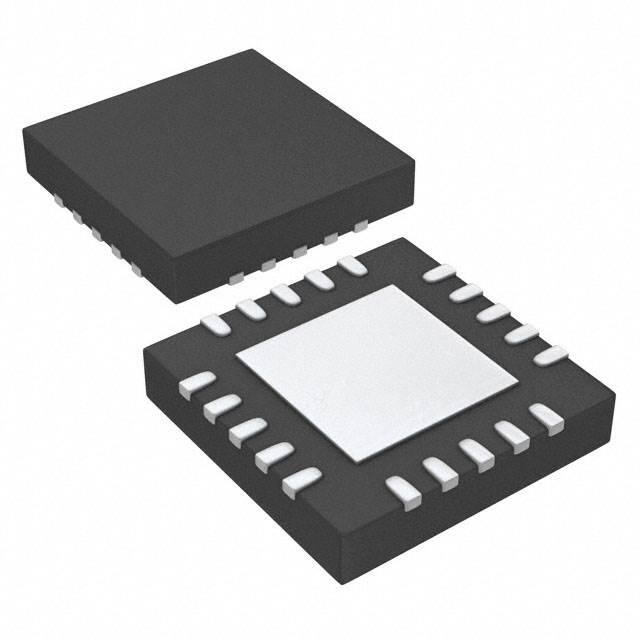
Device Information(1)
PART NUMBER
TPS7A47-Q1
PACKAGE
VQFN (20)
BODY SIZE (NOM)
5.00 mm × 5.00 mm
(1) For all available packages, see the orderable addendum at
the end of the datasheet.
Simplified Schematic
8V
VIN
IN
EN1
EN
5V
TPS7A47-Q1 OUT
VCC1
High-Performance DAC
VIN
IN
EN1
EN
3.3 V
TPS7A47-Q1 OUT
VDD
Copyright © 2017, Texas Instruments Incorporated
1
An IMPORTANT NOTICE at the end of this data sheet addresses availability, warranty, changes, use in safety-critical applications,
intellectual property matters and other important disclaimers. PRODUCTION DATA.
�TPS7A47-Q1
SBVS118 – AUGUST 2017
www.ti.com
Table of Contents
1
2
3
4
5
6
7
Features ..................................................................
Applications ...........................................................
Description .............................................................
Revision History.....................................................
Pin Configuration and Functions .........................
Specifications.........................................................
1
1
1
2
3
4
6.1
6.2
6.3
6.4
6.5
6.6
4
4
5
5
6
7
Absolute Maximum Ratings ......................................
ESD Ratings..............................................................
Recommended Operating Conditions.......................
Thermal Information ..................................................
Electrical Characteristics...........................................
Typical Characteristics ..............................................
8
8.1 Application Information............................................ 15
8.2 Typical Application ................................................. 15
9
Overview .................................................................
Functional Block Diagram .......................................
Feature Description.................................................
Device Functional Modes........................................
Programming...........................................................
Power Supply Recommendations...................... 19
9.1 Power Dissipation (PD)............................................ 19
10 Layout................................................................... 20
10.1
10.2
10.3
10.4
Layout Guidelines .................................................
Layout Example ....................................................
Thermal Protection................................................
Estimating Junction Temperature .........................
20
20
21
21
11 Device and Documentation Support ................. 22
11.1
11.2
11.3
11.4
11.5
11.6
Detailed Description ............................................ 11
7.1
7.2
7.3
7.4
7.5
Application and Implementation ........................ 15
11
11
11
12
12
Documentation Support ........................................
Receiving Notification of Documentation Updates
Community Resources..........................................
Trademarks ...........................................................
Electrostatic Discharge Caution ............................
Glossary ................................................................
22
22
22
22
22
22
12 Mechanical, Packaging, and Orderable
Information ........................................................... 22
4 Revision History
2
DATE
REVISION
NOTES
August 2017
*
Initial release.
Submit Documentation Feedback
Copyright © 2017, Texas Instruments Incorporated
Product Folder Links: TPS7A47-Q1
�TPS7A47-Q1
www.ti.com
SBVS118 – AUGUST 2017
5 Pin Configuration and Functions
OUT
NC
NC
NC
IN
20
19
18
17
16
RGW Package
5-mm × 5-mm, 20-Pin VQFN
Top View
OUT
1
15
IN
NC
2
14
NR
SENSE/FB
3
13
EN
6P4V2
4
12
0P1V
6P4V1
5
11
0P2V
6
7
8
9
10
3P2V
GND
1P6V
0P8V
0P4V
PowerPAD
Not to scale
Pin Functions
PIN
I/O
DESCRIPTION
NAME
NO.
0P1V
12
I
When connected to GND, this pin adds 0.1 V to the nominal output voltage of the regulator.
Do not connect any voltage other than GND to this pin. If not used, leave this pin floating.
0P2V
11
I
When connected to GND, this pin adds 0.2 V to the nominal output voltage of the regulator.
Do not connect any voltage other than GND to this pin. If not used, leave this pin floating.
0P4V
10
I
When connected to GND, this pin adds 0.4 V to the nominal output voltage of the regulator.
Do not connect any voltage other than GND to this pin. If not used, leave this pin floating.
0P8V
9
I
When connected to GND, this pin adds 0.8 V to the nominal output voltage of the regulator.
Do not connect any voltage other than GND to this pin. If not used, leave this pin floating.
1P6V
8
I
When connected to GND, this pin adds 1.6 V to the nominal output voltage of the regulator.
Do not connect any voltage other than GND to this pin. If not used, leave this pin floating.
3P2V
6
I
When connected to GND, this pin adds 3.2 V to the nominal output voltage of the regulator.
Do not connect any voltage other than GND to this pin. If not used, leave this pin floating.
6P4V1
5
I
When connected to GND, this pin adds 6.4 V to the nominal output voltage of the regulator.
Do not connect any voltage other than GND to this pin. If not used, leave this pin floating.
6P4V2
4
I
When connected to GND, this pin adds 6.4 V to the nominal output voltage of the regulator.
Do not connect any voltage other than GND to this pin. If not used, leave this pin floating.
EN
13
I
Enable pin. The device is enabled when the voltage on this pin exceeds the maximum
enable voltage, VEN(HI). If enable is not required, tie EN to IN.
GND
7
—
Ground
Input supply. A capacitor greater than or equal to 1 µF must be tied from this pin to ground to
assure stability.
A 10-µF capacitor is recommended to be connected from IN to GND (as close to the device
as possible) to reduce circuit sensitivity to printed circuit board (PCB) layout, especially when
long input traces or high source impedances are encountered.
IN
15, 16
I
NC
2, 17-19
—
This pin can be left open or tied to any voltage between GND and IN.
NR
14
—
Noise-reduction pin. When a capacitor is connected from this pin to GND, RMS noise can be
reduced to very low levels. A capacitor greater than or equal to 10 nF must be tied from this
pin to ground to assure stability. A 1-µF capacitor is recommended to be connected from NR
to GND (as close to the device as possible) to maximize ac performance and minimize noise.
Submit Documentation Feedback
Copyright © 2017, Texas Instruments Incorporated
Product Folder Links: TPS7A47-Q1
3
�TPS7A47-Q1
SBVS118 – AUGUST 2017
www.ti.com
Pin Functions (continued)
PIN
NAME
NO.
OUT
1, 20
I/O
DESCRIPTION
O
Regulator output. A capacitor greater than or equal to 10 µF must be tied from this pin to
ground to assure stability. A 47-µF ceramic output capacitor is highly recommended to be
connected from OUT to GND (as close to the device as possible) to maximize ac
performance.
Control-loop error amplifier input.
This pin is the SENSE pin if the device output voltage is programmed using ANY-OUT (no
external feedback resistors). This pin must be connected to OUT. Connect this pin to the
point of load to maximize accuracy.
This pin is the FB pin if the device output voltage is set using external resistors. See the
Adjustable Operation Adjustable Operation section for more details.
SENSE/FB
3
I
PowerPAD
Pad
—
Connect the PowerPAD to a large-area ground plane. The PowerPAD™ is internally
connected to GND.
6 Specifications
6.1 Absolute Maximum Ratings
over junction temperature range (unless otherwise noted) (1)
Voltage (2)
Current
(2)
(3)
MAX
–0.4
36
EN pin to GND pin
–0.4
36
EN pin to IN pin
–36
0.4
OUT pin to GND pin
–0.4
VI + 0.3
NR pin to GND pin
–0.4
VI + 0.3 (3)
SENSE/FB pin to GND pin
–0.4
VI + 0.3
0P1V pin to GND pin
–0.4
2.5
0P2V pin to GND pin
–0.4
2.5
0P4V pin to GND pin
–0.4
2.5
0P8V pin to GND pin
–0.4
2.5
1P6V pin to GND pin
–0.4
2.5
3P2V pin to GND pin
–0.4
2.5
6P4V1 pin to GND pin
–0.4
2.5
6P4V2 pin to GND pin
–0.4
2.5
Peak output
Temperature
(1)
MIN
IN pin (VI) to GND pin
UNIT
V
Internally limited
Operating virtual junction, TJ
–40
145
Storage, Tstg
–65
150
°C
Stresses beyond those listed under Absolute Maximum Ratings may cause permanent damage to the device. These are stress ratings
only, which do not imply functional operation of the device at these or any other conditions beyond those indicated under Recommended
Operating Conditions. Exposure to absolute-maximum-rated conditions for extended periods may affect device reliability.
All voltages are with respect to the network ground terminal.
The absolute maximum rating is VI + 0.3 V or 22 V, whichever is smaller.
6.2 ESD Ratings
VALUE
V(ESD)
(1)
4
Electrostatic discharge
Human-body model (HBM), per AEC Q100-002
(1)
Charged-device model (CDM), per AEC Q100-011
±2500
±500
UNIT
V
AEC Q100-002 indicates that HBM stressing shall be in accordance with the ANSI/ESDA/JEDEC JS-001 specification.
Submit Documentation Feedback
Copyright © 2017, Texas Instruments Incorporated
Product Folder Links: TPS7A47-Q1
�TPS7A47-Q1
www.ti.com
SBVS118 – AUGUST 2017
6.3 Recommended Operating Conditions
over junction temperature range (unless otherwise noted)
MIN
NOM
MAX
UNIT
VI
Input voltage
3.0
COUT
Output capacitor
10
35.0
V
V+EN(HI)
Enable high-level voltage
2.0
VI
V
V+EN(LO)
Enable low-level voltage
0
0.4
V
IO
Output current
TJ
Operating junction temperature
µF
0
1.0
A
–40
145
°C
6.4 Thermal Information
TPS7A47-Q1
THERMAL METRIC (1)
RGW (VQFN)
UNIT
20 PINS
RθJA
Junction-to-ambient thermal resistance
31.1
°C/W
RθJC(top)
Junction-to-case (top) thermal resistance
21.1
°C/W
RθJB
Junction-to-board thermal resistance
10.2
°C/W
ψJT
Junction-to-top characterization parameter
0.2
°C/W
ψJB
Junction-to-board characterization parameter
10.2
°C/W
RθJC(bot)
Junction-to-case (bottom) thermal resistance
1.9
°C/W
(1)
For more information about traditional and new thermal metrics, see the Semiconductor and IC Package Thermal Metrics application
report.
Submit Documentation Feedback
Copyright © 2017, Texas Instruments Incorporated
Product Folder Links: TPS7A47-Q1
5
�TPS7A47-Q1
SBVS118 – AUGUST 2017
www.ti.com
6.5 Electrical Characteristics
at –40°C ≤ TJ ≤ 145°C; VI = VO(nom) + 1.0 V or VI = 3.0 V (whichever is greater); VEN = VI; IO = 0 mA; CIN = 10 µF; COUT = 10
µF; CNR = 10 nF; SENSE/FB tied to OUT; and 0P1V, 0P2V, 0P4V, 0P8V, 1P6V, 3P2V, 6P4V1, 6P4V2 pins open (unless
otherwise noted)
PARAMETER
VUVLO
Undervoltage lockout threshold
V(REF)
Reference voltage
VUVLO(HYS)
Under-voltage lockout hysteresis
VNR
Noise reduction pin voltage
VO
Output voltage range
TEST CONDITIONS
MIN
TYP
VI rising
2.67
VI falling
2.5
V(REF) = V(FB),
MAX
UNIT
V
1.4
V
177
mV
Using ANY-OUT option
VOUT
In adjustable mode only
1.4
V
COUT = 20 µF, using ANY-OUT option
1.4
20.5
COUT = 20 µF, using adjustable option
1.4
34
V
Nominal VO accuracy
TJ = 25°C, COUT = 20 µF
–1.0
1.0
%VO
Overall VO accuracy
VO(nom) + 1.0 V ≤ VI ≤ 35 V,
0 mA ≤ IO ≤ 1 A, COUT = 20 µF
–2.5
2.5
%VO
ΔVO(ΔVI)
Line regulation
VO(nom) + 1.0 V ≤ VI ≤ 35 V
0.092
%VO
ΔVO(ΔIO)
Load regulation
0 mA ≤ IO ≤ 1 A
0.3
%VO
VI = 95% VO(nom), IO = 0.5 A
216
VI = 95% VO(nom), IO = 1 A
307
V(DO)
Dropout voltage
I(CL)
Current limit
I(GND)
Ground pin current
I(EN)
Enable pin current
I(SHDN)
Shutdown supply current
I(FB)
Feedback pin current
PSRR
Power-supply rejection ratio
Vn
Output noise voltage
Tsd
6
Thermal shutdown temperature
VO = 90% VO(nom)
IO = 0 mA
1
450
1.26
0.58
mV
A
1.0
IO = 1 A
6.1
VEN = VI
0.78
2
VI = VEN = 35 V
0.81
2
VEN = 0.4 V
2.55
8
VEN = 0.4 V, VI = 35 V
3.04
60
mA
µA
µA
350
nA
VI = 16 V, VO(nom) = 15 V, COUT = 50 µF,
IO = 500 mA, CNR = 1 µF, f = 1 kHz
78
dB
VI = 3 V, VO(nom) = 1.4 V, COUT = 50 µF,
CNR = 1 µF, BW = 10 Hz to 100 kHz
4.17
VIN = 6 V, VO(nom) = 5 V, COUT = 50 µF,
CNR = 1 µF, BW = 10 Hz to 100 kHz
4.67
Shutdown, temperature increasing
170
Reset, temperature decreasing
150
Submit Documentation Feedback
µVRMS
°C
Copyright © 2017, Texas Instruments Incorporated
Product Folder Links: TPS7A47-Q1
�TPS7A47-Q1
www.ti.com
SBVS118 – AUGUST 2017
6.6 Typical Characteristics
at TJ = 25°C; VI = VO(nom) + 1.0 V or VI = 3.0 V (whichever is greater); VEN = VI; IO = 0 mA; CIN = 10 µF; COUT = 10 µF; CNR =
1 µF; SENSE/FB tied to OUT; and 0P1V, 0P2V, 0P4V, 0P8V, 1P6V, 3P2V, 6P4V1, 6P4V2 pins open (unless otherwise
noted)
VOUT = 1.4 V, VNOISE = 4.17 mVRMS
VOUT = 5 V, VNOISE = 4.67 mVRMS
VOUT = 10 V, VNOISE = 7.25 mVRMS
VOUT = 15 V, VNOISE = 12.28 mVRMS
2
VOUT(NOM) (%)
Noise (mV
Hz)
10
−40°C
0°C
+25°C
+85°C
+125°C
3
1
1
0
−1
−2
0.1
−3
0.01
10
100
1k
10k
Frequency (Hz)
100k
−4
1M
0
5
10
15
20
25
Input Voltage (V)
30
35
40
IOUT = 500 mA, COUT = 50 µF, CNR = 1 µF,
BWRMSNOISE (10 Hz, 100 kHz)
Figure 1. Noise vs Output Voltage
−40°C
0°C
+25°C
+85°C
+125°C
3
2
1
0
2.8
2.7
−1
2.6
2.5
2.4
2.3
−2
2.2
−3
−4
UVLO Threshold Off
UVLO Threshold On
2.9
VIN (V)
VOUT(NOM) (%)
Figure 2. Line Regulation
2.1
0
2
−40 −25 −10
100 200 300 400 500 600 700 800 900 1000
Output Current (mA)
Figure 3. Load Regulation
5
20 35 50 65
Temperature (°C)
80
95
110 125
Figure 4. Input Voltage Threshold vs Temperature
2.7
800
2.4
1.8
IQ (µA)
VEN (V)
2.1
1.5
1.2
600
400
−40°C
0°C
+25°C
+105°C
+125°C
0.9
200
0.6
0.3
0
−40 −25 −10
5
20 35 50 65
Temperature (°C)
80
95
110 125
0
0
5
10
15
20
25
Input Voltage (V)
30
35
40
IOUT = 0 µA
Figure 5. Enable Voltage Threshold vs Temperature
Figure 6. Quiescent Current vs Input Voltage
Submit Documentation Feedback
Copyright © 2017, Texas Instruments Incorporated
Product Folder Links: TPS7A47-Q1
7
�TPS7A47-Q1
SBVS118 – AUGUST 2017
www.ti.com
Typical Characteristics (continued)
at TJ = 25°C; VI = VO(nom) + 1.0 V or VI = 3.0 V (whichever is greater); VEN = VI; IO = 0 mA; CIN = 10 µF; COUT = 10 µF; CNR =
1 µF; SENSE/FB tied to OUT; and 0P1V, 0P2V, 0P4V, 0P8V, 1P6V, 3P2V, 6P4V1, 6P4V2 pins open (unless otherwise
noted)
−40°C
0°C
+25°C
+85°C
+125°C
1.8
1.6
IEN (µA)
IGND (mA)
1.4
1
−40°C
0°C
+25°C
+85°C
+125°C
0.1
1
10
100
Output Current (mA)
1.2
1
0.8
0.6
0.4
0.2
0
1000
0
Figure 7. Ground Current vs Output Current
8
15
20
25
Input Voltage (V)
30
35
40
6
2.5
2
ICL (A)
ISHDN (µA)
7
10
Figure 8. Enable Current vs Input Voltage
−40°C
0°C
+25°C
+105°C
+125°C
9
5
5
1.5
4
1
3
2
−40°C
0°C
+25°C
+85°C
+125°C
0.5
1
0
0
5
10
15
20
25
Input Voltage (V)
30
35
0
40
0
4
8
12
Input Voltage (V)
16
20
VOUT = 90% VOUT(NOM)
90
90
80
80
70
70
60
50
40
30
CNR = 0.01 mF
CNR = 0.1 mF
CNR = 1 mF
CNR = 2.2 mF
20
10
0
10
100
1k
10k
100k
Frequency (Hz)
1M
IOUT = 1 A, COUT = 50 µF, VIN = 3 V, VOUT = 1.4 V
Figure 11. Power-Supply Rejection Ratio vs
Frequency and CNR
8
Figure 10. Current Limit vs Input Voltage
PSRR (dB)
PSRR (dB)
Figure 9. Shutdown Current vs Input Voltage
10M
60
50
40
30
CNR = 0.01 mF
CNR = 0.1 mF
CNR = 1 mF
CNR = 2.2 mF
20
10
0
10
100
1k
10k
100k
Frequency (Hz)
1M
10M
IOUT = 0.5 A, COUT = 50 µF, VIN = 3 V, VOUT = 1.4 V
Figure 12. Power-Supply Rejection Ratio vs
Frequency and CNR
Submit Documentation Feedback
Copyright © 2017, Texas Instruments Incorporated
Product Folder Links: TPS7A47-Q1
�TPS7A47-Q1
www.ti.com
SBVS118 – AUGUST 2017
Typical Characteristics (continued)
90
90
80
80
70
70
PSRR (dB)
PSRR (dB)
at TJ = 25°C; VI = VO(nom) + 1.0 V or VI = 3.0 V (whichever is greater); VEN = VI; IO = 0 mA; CIN = 10 µF; COUT = 10 µF; CNR =
1 µF; SENSE/FB tied to OUT; and 0P1V, 0P2V, 0P4V, 0P8V, 1P6V, 3P2V, 6P4V1, 6P4V2 pins open (unless otherwise
noted)
60
50
40
30
10
0
10
100
1k
10k
100k
Frequency (Hz)
1M
50
40
30
IOUT = 0 mA
IOUT = 50 mA
IOUT = 500 mA
IOUT = 1000 mA
20
60
VDO = 200 mV
VDO = 300 mV
VDO = 500 mV
VDO = 1 V
20
10
0
10M
CNR = 1 µF, COUT = 50 µF, VIN = 3 V, VOUT = 1.4 V
10
50
40
VDO = 500 mV
VDO = 1 V
60
50
40
30
30
20
20
10
10
10
100
1k
10k
100k
Frequency (Hz)
1M
0
10M
VOUT = 3.3 V, CNR = 1 µF, COUT = 50 µF, IOUT = 500 mA
10
80
70
70
PSRR (dB)
90
80
60
50
40
VOUT = 1.4 V
VOUT = 3.3 V
VOUT = 5 V
VOUT = 10 V
VOUT = 15 V
20
10
10
100
1k
Figure 17. Power-Supply Rejection Ratio vs
Frequency and VOUT
10M
40
VOUT = 1.4 V
VOUT = 3.3 V
VOUT = 5 V
VOUT = 10 V
VOUT = 15 V
10
CNR = 1 µF, COUT = 50 µF, IOUT = 500 mA
1M
50
20
1M
10k
100k
Frequency (Hz)
60
30
10k
100k
Frequency (Hz)
1k
Figure 16. Power-Supply Rejection Ratio vs
Frequency and VDO
90
30
100
VOUT = 3.3 V, CNR = 1 µF, COUT = 50 µF, IOUT = 1 A
Figure 15. Power-Supply Rejection Ratio vs
Frequency and VDO
PSRR (dB)
10M
70
60
0
1M
80
PSRR (dB)
PSRR (dB)
VDO = 200 mV
VDO = 300 mV
90
70
0
10k
100k
Frequency (Hz)
Figure 14. Power-Supply Rejection Ratio vs
Frequency and VDO
VDO = 200 mV
VDO = 300 mV
VDO = 500 mV
VDO = 1 V
80
1k
VOUT = 3.3 V, CNR = 1 µF, COUT = 50 µF, IOUT = 50 mA
Figure 13. Power-Supply Rejection Ratio vs
Frequency and IO
90
100
10M
0
10
100
1k
10k
100k
Frequency (Hz)
1M
10M
CNR = 1 µF, COUT = 50 µF, IOUT = 1000 mA
Figure 18. Power-Supply Rejection Ratio vs
Frequency and VOUT
Submit Documentation Feedback
Copyright © 2017, Texas Instruments Incorporated
Product Folder Links: TPS7A47-Q1
9
�TPS7A47-Q1
SBVS118 – AUGUST 2017
www.ti.com
Typical Characteristics (continued)
at TJ = 25°C; VI = VO(nom) + 1.0 V or VI = 3.0 V (whichever is greater); VEN = VI; IO = 0 mA; CIN = 10 µF; COUT = 10 µF; CNR =
1 µF; SENSE/FB tied to OUT; and 0P1V, 0P2V, 0P4V, 0P8V, 1P6V, 3P2V, 6P4V1, 6P4V2 pins open (unless otherwise
noted)
IOUT
(1 A/div)
VIN
(10 V/div)
VOUT
(10 mV/div)
VOUT
(10 mV/div)
Time (500 ms/div)
Time (5 ms/div)
VIN = 5 V, VOUT = 3.3 V, IOUT = 10 mA to 845 mA
VIN = 5 V to 15 V, VOUT = 3.3 V, IOUT = 845 mA
Figure 19. Load Transient
Figure 20. Line Transient
IOUT = 50 mA, VNOISE = 5 mVRMS
IOUT = 20 mA, VNOISE = 5.9 mVRMS
VEN
(2 V/div)
Hz)
10
Noise (mV
VOUT
(2 V/div)
IOUT
(200 mA/div)
1
0.1
0.01
Time (50 ms/div)
Startup time = 65 ms, VIN = 6 V, VOUT = 5V, IOUT = 500 mA,
CIN = 10 µF, COUT = 50 µF
10
100
1k
10k
Frequency (Hz)
100k
1M
VOUT = 4.7 V, COUT = 10 µF, CNR = 1 µF, BWRMSNOISE (10 Hz,
100 kHz)
Figure 21. Startup
Figure 22. Noise vs Output Current
10
Submit Documentation Feedback
Copyright © 2017, Texas Instruments Incorporated
Product Folder Links: TPS7A47-Q1
�TPS7A47-Q1
www.ti.com
SBVS118 – AUGUST 2017
7 Detailed Description
7.1 Overview
The TPS7A47-Q1 is a positive voltage (35 V), ultralow-noise (4.2 µVRMS) LDO capable of sourcing a 1-A load.
The TPS7A47-Q1 is designed with bipolar technology primarily for high-accuracy, high-precision instrumentation
applications where clean voltage rails are critical to maximize system performance. This feature makes the
device ideal for powering operational amplifiers, analog-to-digital converters (ADCs), digital-to-analog converters
(DACs), and other high-performance analog circuitry.
7.2 Functional Block Diagram
IN
OUT
Thermal
Shutdown
UVLO
IN
OUT
CIN
COUT
Current
Limit
100 kW
Band
Gap
265.5 kW
SENSE/FB
3.2 MW
0P1V
1.6 MW
1.572 MW
0P2V
800 kW
Fast
Charge
0P4V
Enable
EN
400 kW
50 kW
50 kW
100 kW
200 kW
0P8V
1P6V 3P2V 6P4V 6P4V
TI Device
NR
CNR
Copyright © 2016, Texas Instruments Incorporated
7.3 Feature Description
7.3.1 Internal Current Limit (ICL)
The internal current limit circuit is used to protect the LDO against high-load current faults or shorting events. The
LDO is not designed to operate at a steady-state current limit. During a current-limit event, the LDO sources
constant current. Therefore, the output voltage falls when load impedance decreases. Also, when a current limit
occurs while the resulting output voltage is low, excessive power is dissipated across the LDO, which results in a
thermal shutdown of the output.
7.3.2 Enable (EN) And Undervoltage Lockout (UVLO)
The TPS7A47-Q1 only turns on when both EN and UVLO are above the respective voltage thresholds. The
UVLO circuit monitors input voltage (VI) to prevent device turn-on before VI rises above the lockout voltage. The
UVLO circuit also causes a shutdown when VI falls below lockout. The EN signal allows independent logic-level
turn-on and shutdown of the LDO when the input voltage is present. EN can be connected directly to VI if
independent turn-on is not needed.
Submit Documentation Feedback
Copyright © 2017, Texas Instruments Incorporated
Product Folder Links: TPS7A47-Q1
11
�TPS7A47-Q1
SBVS118 – AUGUST 2017
www.ti.com
Feature Description (continued)
7.3.3 Soft-Start And Inrush Current
Soft-start refers to the ramp-up characteristic of the output voltage during LDO turn-on after EN and UVLO have
achieved the threshold voltage. The noise-reduction capacitor serves a dual purpose of both governing output
noise reduction and programming the soft-start ramp during turn-on.
Inrush current is defined as the current through the LDO from IN to OUT during the time of the turn-on ramp up.
Inrush current then consists primarily of the sum of load and charge current to the output capacitor. Use
Equation 1 to estimate in-rush current:
VOUT(t)
COUT ´ dVOUT(t)
IOUT(t) =
+
RLOAD
dt
where:
•
•
•
VOUT(t) is the instantaneous output voltage of the turn-on ramp
dVOUT(t) / dt is the slope of the VO ramp
RLOAD is the resistive load impedance
(1)
7.4 Device Functional Modes
The TPS7A47-Q1 has the following functional modes:
1. Enabled: when EN goes above V+EN(HI), the device is enabled.
2. Disabled: when EN goes below V+EN(LO), the device is disabled. During this time, OUT is high impedance,
and the current into IN does not exceed I(SHDN).
7.5 Programming
7.5.1 ANY-OUT Programmable Output Voltage
For ANY-OUT operation, do not use external resistors to set the output voltage, but use device pins 4, 5, 6, 8, 9,
10, 11, and 12 to program the regulated output voltage. Each pin is either connected to ground (active) or is left
open (floating). The ANY-OUT programming is set by Equation 2 as the sum of the internal reference voltage
(V(REF) = 1.4 V) plus the accumulated sum of the respective voltages assigned to each active pin; that is, 100 mV
(pin 12), 200 mV (pin 11), 400 mV (pin 10), 800 mV (pin 9), 1.6 V (pin 8), 3.2 V (pin 6), 6.4 V (pin 5), or 6.4 V
(pin 4). Table 1 summarizes these voltage values associated with each active pin setting for reference. By
leaving all program pins open, or floating, the output is thereby programmed to the minimum possible output
voltage equal to V(REF).
VOUT = VREF + (S ANY-OUT Pins to Ground)
(2)
Table 1. ANY-OUT Programmable Output Voltage
12
ANY-OUT PROGRAM PINS (Active Low)
ADDITIVE OUTPUT VOLTAGE LEVEL
Pin 4 (6P4V2)
6.4 V
Pin 5 (6P4V1)
6.4 V
Pin 6 (3P2)
3.2 V
Pin 8 (1P6)
1.6 V
Pin 9 (0P8)
800 mV
Pin 10 (0P4)
400 mV
Pin 11 (0P2)
200 mV
Pin 12 (0P1)
100 mV
Submit Documentation Feedback
Copyright © 2017, Texas Instruments Incorporated
Product Folder Links: TPS7A47-Q1
�TPS7A47-Q1
www.ti.com
SBVS118 – AUGUST 2017
Table 2 shows a list of the most common output voltages and the corresponding pin settings. The voltage setting
pins have a binary weight; therefore, the output voltage can be programmed to any value from 1.4 V to 20.5 V in
100-mV steps.
Table 2. Common Output Voltages and Corresponding Pin Settings
PIN NAMES AND VOLTAGE PER PIN
VO (V)
0P1V
(100 mV)
0P2V
(200 mV)
0P4V
(400 mV)
0P8V
(800 mV)
1P6V
(1.6 V)
3P2V
(3.2 V)
6P4V1
(6.4 V)
6P4V2
(6.4 V)
1.4
Open
Open
Open
Open
Open
Open
Open
Open
1.5
GND
Open
Open
Open
Open
Open
Open
Open
1.8
Open
Open
GND
Open
Open
Open
Open
Open
2.5
GND
GND
Open
GND
Open
Open
Open
Open
3
Open
Open
Open
Open
GND
Open
Open
Open
3.3
GND
GND
Open
Open
GND
Open
Open
Open
4.5
GND
GND
GND
GND
GND
Open
Open
Open
5
Open
Open
GND
Open
Open
GND
Open
Open
10
Open
GND
GND
Open
GND
Open
GND
Open
12
Open
GND
Open
GND
Open
GND
GND
Open
15
Open
Open
Open
GND
Open
Open
GND
GND
18
Open
GND
GND
Open
Open
GND
GND
GND
20.5
GND
GND
GND
GND
GND
GND
GND
GND
7.5.2 Adjustable Operation
The TPS7A47-Q1 has an output voltage range of 1.4 V to 34 V. For adjustable operation, set the nominal output
voltage of the device (as shown in Figure 23) using two external resistors.
VIN
CIN
10 mF
CNR/SS
1 mF
IN
VOUT
OUT
R1
TPS7A4701-Q1
EN
FB
NR
GND
R2
COUT
47 mF
Copyright © 2016, Texas Instruments Incorporated
Figure 23. Adjustable Operation for Maximum AC Performance
R1 and R2 can be calculated for any output voltage within the operational range. The current through feedback
resistor R2 must be at least 5 µA to ensure stability. Additionally, the current into the FB pin (I(FB), typically
350 nA) creates an additional output voltage offset that depends on the resistance of R1. For high-accuracy
applications, select R2 such that the current through R2 is at least 35 µA to minimize any effects of I(FB) variation
on the output voltage; 10 kΩ is recommended. Equation 3 calculates R1.
V
- VREF
R1 = OUT
V
IFB + REF
R2
where
•
•
VREF = 1.4 V
IFB = 350 nA
(3)
Use 0.1% tolerance resistors to minimize the effects of resistor inaccuracy on the output voltage.
Submit Documentation Feedback
Copyright © 2017, Texas Instruments Incorporated
Product Folder Links: TPS7A47-Q1
13
�TPS7A47-Q1
SBVS118 – AUGUST 2017
www.ti.com
Table 3 shows the resistor combinations to achieve some standard rail voltages with commercially available 1%
tolerance resistors. The resulting output voltages yield a nominal error of < 0.5%.
Table 3. Suggested Resistors for Common Voltage Rails
VOUT
R1, CALCULATED
R1, CLOSEST 1% VALUE
R2
1.4 V
0Ω
0Ω
∞
1.8 V
2.782 kΩ
2.8 kΩ
9.76 kΩ
3.3 V
13.213 kΩ
13.3 kΩ
9.76 kΩ
5V
25.650 kΩ
25.5 kΩ
10 kΩ
12 V
77.032 kΩ
76.8 kΩ
10.2 kΩ
15 V
101.733 kΩ
102 kΩ
10.5 kΩ
18 V
118.276 kΩ
118 kΩ
10 kΩ
24 V
164.238 kΩ
165 kΩ
10.2 kΩ
To achieve higher nominal accuracy, two resistors can be used in the place of R1. Select the two resistor values
such that the sum results in a value as close as possible to the calculated R1 value.
There are several alternative ways to set the output voltage. The program pins can be pulled low using external
general-purpose input/output pins (GPIOs), or can be hardwired by the given layout of the printed circuit board
(PCB) to set the ANY-OUT voltage. The TPS7A4701 evaluation module (EVM), available for purchase from the
TI eStore, allows the output voltage to be programmed using jumpers.
14
Submit Documentation Feedback
Copyright © 2017, Texas Instruments Incorporated
Product Folder Links: TPS7A47-Q1
�TPS7A47-Q1
www.ti.com
SBVS118 – AUGUST 2017
8 Application and Implementation
NOTE
Information in the following applications sections is not part of the TI component
specification, and TI does not warrant its accuracy or completeness. TI’s customers are
responsible for determining suitability of components for their purposes. Customers should
validate and test their design implementation to confirm system functionality.
8.1 Application Information
The TPS7A47-Q1 is a high-voltage, low-noise, 1-A LDO. Low-noise performance makes this LDO ideal for
providing rail voltages to noise-sensitive loads, such as PLLs, oscillators, and high-speed ADCs.
8.2 Typical Application
As shown in Figure 24, output voltage is set by grounding the appropriate control pins. When grounded, all
control pins add a specific voltage on top of the internal reference voltage (V(REF) = 1.4 V). For example, when
grounding pins 0P1V, 0P2V, and 1P6V, the voltage values 0.1 V, 0.2 V, and 1.6 V are added to the 1.4-V
internal reference voltage for VO(nom) equal to 3.3 V, as described in the Programming section.
VIN = 5 V
IN
VOUT = 3.3 V
OUT
10 mF
47 mF
EN
NR
1 mF
0P1V
TPS7A4701-Q1
SENSE
Load
GND
0P2V
0P4V 0P8V 1P6V 3P2V 6P4V1 6P4V2
Copyright © 2016, Texas Instruments Incorporated
Figure 24. Typical Application, VOUT = 3.3 V
8.2.1 Design Requirements
PARAMETER
DESIGN REQUIREMENT
Input voltage
5.0 V, ±10%
Output voltage
3.3 V, ±3%
Output current
500 mA
Peak-to-peak noise, 10 Hz to 100 kHz
50 µVPP
8.2.2 Detailed Design Procedure
8.2.2.1 Capacitor Recommendations
This LDO is designed to be stable using low equivalent series resistance (ESR), ceramic capacitors at the input,
output, and at the noise-reduction pin (NR, pin 14). Multilayer ceramic capacitors have become the industry
standard for these types of applications and are recommended here, but must be used with good judgment.
Ceramic capacitors that employ X7R-, X5R-, and COG-rated dielectric materials provide relatively good
capacitive stability across temperature, but the use of Y5V-rated capacitors is discouraged precisely because the
capacitance varies so widely. In all cases, ceramic capacitance varies a great deal with operating voltage and the
design engineer must be aware of these characteristics. TI recommends applying a 50% derating of the nominal
capacitance in the design.
Submit Documentation Feedback
Copyright © 2017, Texas Instruments Incorporated
Product Folder Links: TPS7A47-Q1
15
�TPS7A47-Q1
SBVS118 – AUGUST 2017
www.ti.com
Attention must be given to the input capacitance to minimize transient input droop during load current steps
because the TPS7A47-Q1 has a very fast load transient response. Large input capacitors are necessary for good
transient load response, and have no detrimental influence on the stability of the device. However, using large
ceramic input capacitances can also cause unwanted ringing at the output if the input capacitor, in combination
with the wire lead inductance, creates a high-Q peaking effect during transients. For example, a 5-nH lead
inductance and a 10-µF input capacitor form an LC filter with a resonance frequency of 712 kHz at the edge of
the control loop bandwidth. Short, well-designed interconnect leads to the up-stream supply minimize this effect
without adding damping. Damping of unwanted ringing can be accomplished by using a tantalum capacitor, with
a few hundred milliohms of ESR, in parallel with the ceramic input capacitor.
8.2.2.1.1 Input and Output Capacitor Requirements
The TPS7A47-Q1 is designed and characterized for operation with ceramic capacitors of 10 µF or greater at the
input and output. Optimal noise performance is characterized using a total output capacitor value of 50 µF. Input
and output capacitances must be located as near as practical to the respective input and output pins.
8.2.2.1.2 Noise-Reduction Capacitor (CNR)
The noise-reduction capacitor, connected to the NR pin of the LDO, forms an RC filter for filtering out noise that
might ordinarily be amplified by the control loop and appear on the output voltage. Larger capacitances, up to
1 µF, affect noise reduction at lower frequencies and also tend to further reduce noise at higher frequencies. CNR
also serves a secondary purpose in programming the turn-on rise time of the output voltage and thereby controls
the turn-on surge current.
8.2.2.2 Dropout Voltage (VDO)
Generally speaking, the dropout voltage often refers to the voltage difference between the input and output
voltage (V(DO) = VI – VO). However, in the Electrical Characteristics V(DO) is defined as the VI – VO voltage at the
rated current (I(RATED)), where the main current pass-FET is fully on in the Ohmic region of operation and is
characterized by the classic RDS(on) of the FET. V(DO) indirectly specifies a minimum input voltage above the
nominal programmed output voltage at which the output voltage is expected to remain within its accuracy
boundary. If the input falls below this V(DO) limit (VI < VO + V(DO)), then the output voltage decreases in order to
follow the input voltage.
Dropout voltage is always determined by the RDS(on) of the main pass-FET. Therefore, if the LDO operates below
the rated current, then V(DO) is directly proportional to the output current and can be reduced by the same factor.
Use Equation 4 to calculate RDS(on) for the TPS7A47-Q1:
VDO
RDS(ON) =
IRATED
(4)
8.2.2.3 Output Voltage Accuracy
The output voltage accuracy specifies minimum and maximum output voltage error, relative to the expected
nominal output voltage stated as a percent. This accuracy error typically includes the errors introduced by the
internal reference and the load and line regulation across the full range of rated load and line operating
conditions over temperature, unless otherwise specified by the Electrical Characteristics. Output voltage
accuracy also accounts for all variations between manufacturing lots.
8.2.2.4 Startup
The startup time for the TPS7A47-Q1 depends on the output voltage and the capacitance of the CNR capacitor.
Equation 5 calculates the startup time for a typical device.
5·
§V
tSS 100,000 ‡ CNR ‡ ln ¨ R
¸
5
©
¹
where
•
•
16
CNR = capacitance of the CNR capacitor
VR = VO voltage if using the ANY-OUT configuration, or 1.4 V if using the adjustable configuration
Submit Documentation Feedback
(5)
Copyright © 2017, Texas Instruments Incorporated
Product Folder Links: TPS7A47-Q1
�TPS7A47-Q1
www.ti.com
SBVS118 – AUGUST 2017
8.2.2.5 AC Performance
AC performance of the LDO is typically understood to include power-supply rejection ratio, load step transient
response, and output noise. These metrics are primarily a function of open-loop gain and bandwidth, phase
margin, and reference noise.
8.2.2.5.1 Power-Supply Rejection Ratio (PSRR)
PSRR is a measure of how well the LDO control loop rejects ripple noise from the input source to make the dc
output voltage as noise-free as possible across the frequency spectrum (usually 10 Hz to 10 MHz). Equation 6
gives the PSRR calculation as a function of frequency where input noise voltage [VS(IN)(f)] and output noise
voltage [VS(OUT)(f)] are understood to be purely ac signals.
VS(IN)(f)
PSRR (dB) = 20 Log10
VS(OUT)(f)
(6)
Noise that couples from the input to the internal reference voltage for the control loop is also a primary
contributor to reduced PSRR magnitude and bandwidth. This reference noise is greatly filtered by the noisereduction capacitor at the NR pin of the LDO in combination with an internal filter resistor (RSS) for optimal
PSRR.
The LDO is often employed not only as a dc/dc regulator, but also to provide exceptionally clean power-supply
voltages that are free of noise and ripple to power-sensitive system components. This usage is especially true for
the TPS7A47-Q1.
8.2.2.5.2 Load Step Transient Response
The load step transient response is the output voltage response by the LDO to a step change in load current
whereby output voltage regulation is maintained. The worst-case response is characterized for a load step of
10 mA to 1 A (at 1 A per microsecond) and shows a classic, critically-damped response of a very stable system.
The voltage response shows a small dip in the output voltage when charge is initially depleted from the output
capacitor and then the output recovers as the control loop adjusts itself. The depth of the charge depletion
immediately after the load step is directly proportional to the amount of output capacitance. However, to some
extent, the speed of recovery is inversely proportional to that same output capacitance. In other words, larger
output capacitances act to decrease any voltage dip or peak occurring during a load step but also decrease the
control-loop bandwidth, thereby slowing response.
The worst-case, off-loading step characterization occurs when the current step transitions from 1 A to 0 mA.
Initially, the LDO loop cannot respond fast enough to prevent a small increase in output voltage charge on the
output capacitor. Because the LDO cannot sink charge current, the control loop must turn off the main pass-FET
to wait for the charge to deplete, thus giving the off-load step its typical monotonic decay (which appears
triangular in shape).
8.2.2.5.3 Noise
The TPS7A47-Q1 is designed, in particular, for system applications where minimizing noise on the power-supply
rail is critical to system performance. This scenario is the case for phase-locked loop (PLL)-based clocking
circuits for instance, where minimum phase noise is all important, or in-test and measurement systems where
even small power-supply noise fluctuations can distort instantaneous measurement accuracy. Because the
TPS7A47-Q1 is also designed for higher voltage industrial applications, the noise characteristic is well designed
to minimize any increase as a function of the output voltage.
LDO noise is defined as the internally-generated intrinsic noise created by the semiconductor circuits alone. This
noise is the sum of various types of noise (such as shot noise associated with current-through-pin junctions,
thermal noise caused by thermal agitation of charge carriers, flicker or 1/f noise that is a property of resistors and
dominates at lower frequencies as a function of 1/f, burst noise, and avalanche noise).
To calculate the LDO RMS output noise, a spectrum analyzer must first measure the spectral noise across the
bandwidth of choice (typically 10 Hz to 100 kHz in units of µV/√Hz). The RMS noise is then calculated in the
usual manner as the integrated square root of the squared spectral noise over the band, then averaged by the
bandwidth.
Submit Documentation Feedback
Copyright © 2017, Texas Instruments Incorporated
Product Folder Links: TPS7A47-Q1
17
�TPS7A47-Q1
SBVS118 – AUGUST 2017
www.ti.com
8.2.3 Application Curves
VOUT (10 µV/DIV)
VEN (2 V/DIV)
VOUT (1 V/DIV)
ILOAD (500 mA/DIV)
Figure 25. Startup With EN Pin Rising
(10 ms per Division)
18
Figure 26. Output Noise Voltage, 10 Hz to 100 kHz
(10 ms per Division)
Submit Documentation Feedback
Copyright © 2017, Texas Instruments Incorporated
Product Folder Links: TPS7A47-Q1
�TPS7A47-Q1
www.ti.com
SBVS118 – AUGUST 2017
9 Power Supply Recommendations
The device is designed to operate from an input voltage supply range of 3 V to 35 V. If the input supply is noisy,
additional input capacitors with low ESR can help improve the output noise performance.
9.1 Power Dissipation (PD)
Power dissipation must be considered in the PCB design. In order to minimize risk of device operation above
145°C, use as much copper area as available for thermal dissipation. Do not locate other power-dissipating
devices near the LDO.
Power dissipation in the regulator depends on the input to output voltage difference and load conditions.
Equation 7 calculates PD:
PD = (VOUT - VIN) ´ IOUT
(7)
Power dissipation can be minimized, and thus greater efficiency achieved, by proper selection of the system
voltage rails. Proper selection allows the minimum input voltage necessary for output regulation to be obtained.
The primary heat conduction path for the VQFN (RGW) package is through the PowerPAD to the PCB. The
PowerPAD must be soldered to a copper pad area under the device. Thermal vias are recommended to improve
the thermal conduction to other layers of the PCB.
The maximum power dissipation determines the maximum allowable junction temperature (TJ) for the device.
According to Equation 8, power dissipation and junction temperature are most often related by the junction-toambient thermal resistance (θJA) of the combined PCB and device package and the temperature of the ambient
air (TA).
TJ = TA + (qJA ´ PD)
(8)
Unfortunately, this thermal resistance (θJA) depends primarily on the heat-spreading capability built into the
particular PCB design, and therefore varies according to the total copper area, copper weight, and location of the
spreading planes. The θJA recorded in the Thermal Information table is determined by the JEDEC standard, PCB,
and copper-spreading area and is to be used only as a relative measure of package thermal performance. For a
well-designed thermal layout, θJA is actually the sum of the VQFN package junction-to-case (bottom) thermal
resistance (θJCbot) plus the thermal resistance contribution by the PCB copper. By knowing θJCbot, the minimum
amount of appropriate heat sinking can be used with Figure 27 to estimate θJA. θJCbot can be found in the
Thermal Information table.
120
100
qJA (°C/W)
80
60
qJA (RGW)
40
20
0
0
1
2
3
4
5
7
6
8
9
10
2
Board Copper Area (in )
2
NOTE: θJA value at a board size of 9-in (that is, 3-in × 3-in) is a JEDEC standard.
Figure 27. θJA vs Board Size
Submit Documentation Feedback
Copyright © 2017, Texas Instruments Incorporated
Product Folder Links: TPS7A47-Q1
19
�TPS7A47-Q1
SBVS118 – AUGUST 2017
www.ti.com
10 Layout
10.1 Layout Guidelines
For best overall performance, all circuit components are recommended to be located on the same side of the
circuit board and as near as practical to the respective LDO pin connections. Ground return connections to the
input and output capacitor, and to the LDO ground pin, must also be as close to each other as possible and
connected by a wide, component-side, copper surface. The use of vias and long traces to create LDO circuit
connections is strongly discouraged and negatively affects system performance. This grounding and layout
scheme minimizes inductive parasitics and thereby reduces load-current transients, minimizes noise, and
increases circuit stability.
A ground reference plane is also recommended. This reference plane serves to assure accuracy of the output
voltage, shield noise, and behaves similar to a thermal plane to spread (or sink) heat from the LDO device when
connected to the PowerPAD. In most applications, this ground plane is necessary to meet thermal requirements.
Use the TPS7A4701 evaluation module (EVM), available for purchase from the TI eStore, as a reference for
layout and application design.
10.2 Layout Example
xxxxxxx
xxxxxxx
xxxxxxx
GND
Signal Ground
10
6
11
5
R1
CNR
EN
SN/FB
NR
NC
NC
NC
1
16
NC
15
R2
20
Power
Ground
Input
CIN
Output
Use R1 and R2
with adjustable
operation
Connect if
ANYOUT
operation is
used.
COUT
Orient input and output capacitors
vertically, so that the grounds are
separated.
Figure 28. Layout Example
20
Submit Documentation Feedback
Copyright © 2017, Texas Instruments Incorporated
Product Folder Links: TPS7A47-Q1
�TPS7A47-Q1
www.ti.com
SBVS118 – AUGUST 2017
10.3 Thermal Protection
The TPS7A47-Q1 contains a thermal shutdown protection circuit to turn off the output current when excessive
heat is dissipated in the LDO. Thermal shutdown occurs when the thermal junction temperature (TJ) of the main
pass-FET exceeds 170°C (typical). Thermal shutdown hysteresis assures that the LDO again resets (turns on)
when the temperature falls to 145°C (typical). Because the TPS7A47-Q1 is capable of supporting high input
voltages, a great deal of power can be expected to be dissipated across the device at low output voltages, which
causes a thermal shutdown. The thermal time-constant of the semiconductor die is fairly short, and thus the
output oscillates on and off at a high rate when thermal shutdown is reached until power dissipation is reduced.
For reliable operation, the junction temperature must be limited to a maximum of 145°C. To estimate the thermal
margin in a given layout, increase the ambient temperature until the thermal protection shutdown is triggered
using worst-case load and highest input voltage conditions. For good reliability, thermal shutdown must be
designed to occur at least 45°C above the maximum expected ambient temperature condition for the application.
This configuration produces a worst-case junction temperature of 145°C at the highest expected ambient
temperature and worst-case load.
The internal protection circuitry of the TPS7A47-Q1 is designed to protect against thermal overload conditions.
The circuitry is not intended to replace proper heat sinking. Continuously running the TPS7A47-Q1 into thermal
shutdown degrades device reliability.
10.4 Estimating Junction Temperature
JEDEC standards recommend the use of PSI thermal metrics to estimate the junction temperatures of the LDO
when in-circuit on a typical PCB board application. These metrics are not strictly speaking thermal resistances,
but rather offer practical and relative means of estimating junction temperatures. These PSI metrics are
determined to be significantly independent of copper-spreading area. The key thermal metrics (ΨJT and ΨJB) are
given in the Thermal Information table and are used in accordance with Equation 9.
YJT: TJ = TT + YJT ´ PD
YJB: TJ = TB + YJB ´ PD
where:
•
•
•
PD is the power dissipated as explained in Equation 7
TT is the temperature at the center-top of the device package
TB is the PCB surface temperature measured 1 mm from the device package and centered on the package
edge
(9)
Submit Documentation Feedback
Copyright © 2017, Texas Instruments Incorporated
Product Folder Links: TPS7A47-Q1
21
�TPS7A47-Q1
SBVS118 – AUGUST 2017
www.ti.com
11 Device and Documentation Support
11.1 Documentation Support
11.1.1 Related Documentation
For related documentation see the following:
• TPS7A33 –36-V, 1-A, Ultralow-Noise Negative Voltage Regulator
• TPS7A47XXEVM-094 Evaluation Module User Guide
• Pros and Cons of Using a Feed-Forward Capacitor with a Low Dropout Regulator
11.2 Receiving Notification of Documentation Updates
To receive notification of documentation updates, navigate to the device product folder on ti.com. In the upper
right corner, click on Alert me to register and receive a weekly digest of any product information that has
changed. For change details, review the revision history included in any revised document.
11.3 Community Resources
The following links connect to TI community resources. Linked contents are provided "AS IS" by the respective
contributors. They do not constitute TI specifications and do not necessarily reflect TI's views; see TI's Terms of
Use.
TI E2E™ Online Community TI's Engineer-to-Engineer (E2E) Community. Created to foster collaboration
among engineers. At e2e.ti.com, you can ask questions, share knowledge, explore ideas and help
solve problems with fellow engineers.
Design Support TI's Design Support Quickly find helpful E2E forums along with design support tools and
contact information for technical support.
11.4 Trademarks
ANY-OUT, PowerPAD, E2E are trademarks of Texas Instruments.
All other trademarks are the property of their respective owners.
11.5 Electrostatic Discharge Caution
This integrated circuit can be damaged by ESD. Texas Instruments recommends that all integrated circuits be handled with
appropriate precautions. Failure to observe proper handling and installation procedures can cause damage.
ESD damage can range from subtle performance degradation to complete device failure. Precision integrated circuits may be more
susceptible to damage because very small parametric changes could cause the device not to meet its published specifications.
11.6 Glossary
SLYZ022 — TI Glossary.
This glossary lists and explains terms, acronyms, and definitions.
12 Mechanical, Packaging, and Orderable Information
The following pages include mechanical, packaging, and orderable information. This information is the most
current data available for the designated devices. This data is subject to change without notice and revision of
this document. For browser-based versions of this data sheet, refer to the left-hand navigation.
22
Submit Documentation Feedback
Copyright © 2017, Texas Instruments Incorporated
Product Folder Links: TPS7A47-Q1
�PACKAGE OPTION ADDENDUM
www.ti.com
10-Dec-2020
PACKAGING INFORMATION
Orderable Device
Status
(1)
Package Type Package Pins Package
Drawing
Qty
Eco Plan
(2)
Lead finish/
Ball material
MSL Peak Temp
Op Temp (°C)
Device Marking
(3)
(4/5)
(6)
TPS7A4701QRGWRQ1
ACTIVE
VQFN
RGW
20
3000
RoHS & Green
NIPDAU
Level-2-260C-1 YEAR
-40 to 125
7A4701Q
TPS7A4701QRGWTQ1
ACTIVE
VQFN
RGW
20
250
RoHS & Green
NIPDAU
Level-2-260C-1 YEAR
-40 to 125
7A4701Q
(1)
The marketing status values are defined as follows:
ACTIVE: Product device recommended for new designs.
LIFEBUY: TI has announced that the device will be discontinued, and a lifetime-buy period is in effect.
NRND: Not recommended for new designs. Device is in production to support existing customers, but TI does not recommend using this part in a new design.
PREVIEW: Device has been announced but is not in production. Samples may or may not be available.
OBSOLETE: TI has discontinued the production of the device.
(2)
RoHS: TI defines "RoHS" to mean semiconductor products that are compliant with the current EU RoHS requirements for all 10 RoHS substances, including the requirement that RoHS substance
do not exceed 0.1% by weight in homogeneous materials. Where designed to be soldered at high temperatures, "RoHS" products are suitable for use in specified lead-free processes. TI may
reference these types of products as "Pb-Free".
RoHS Exempt: TI defines "RoHS Exempt" to mean products that contain lead but are compliant with EU RoHS pursuant to a specific EU RoHS exemption.
Green: TI defines "Green" to mean the content of Chlorine (Cl) and Bromine (Br) based flame retardants meet JS709B low halogen requirements of


 工商网监
湘ICP备2023018690号
工商网监
湘ICP备2023018690号
