TPS7H1101A-SP
TPS7H1101A-SP
SLVSDW6C – APRIL 2017 – REVISED
APRIL 2021
SLVSDW6C – APRIL 2017 – REVISED APRIL 2021
www.ti.com
TPS7H1101A-SP 1.5-V to 7-V Input, 3-A, Radiation-Hardened LDO Regulator
1 Features
•
•
•
•
•
•
•
•
•
•
•
•
•
•
•
5962R13202 (1):
– Radiation hardness assurance (RHA) qualified
up to total ionizing dose (TID) 100 krad(Si)
– ELDRS-free: 100 krad(Si)
– Dose rate: 10 mrad(Si)/s
– Single event latch-up (SEL) immune to
LET = 85 MeV-cm2/mg
– SEB and SEGR immune to
LET = 85 MeV-cm2/mg
– SET/SEFI onset threshold > 40 MeV-cm2/mg(2)
• Specifically designed to always upset low
to avoid damage to critical downstream
component
– SET/SEFI cross-section plot(2)
Ultra-low VIN range: 1.5 V to 7 V
3-A maximum output current
Current share/parallel operation to provide up to
6-A output current
Stable with ceramic output capacitor
±2% accuracy over line, load, and temperature
Programmable soft start through external capacitor
Input enable across all input voltages and powergood output for power sequencing
Ultra-low dropout LDO voltage:
62 mV at 1 A (25°C), VOUT = 1.8 V
Low noise:
20.33 µVRMS, VIN = 2 V, VOUT = 1.8 V at 3 A
PSRR: over 45 dB at 1 kHz
Excellent load/line transient response
Foldback current limit
See the Design and development tab
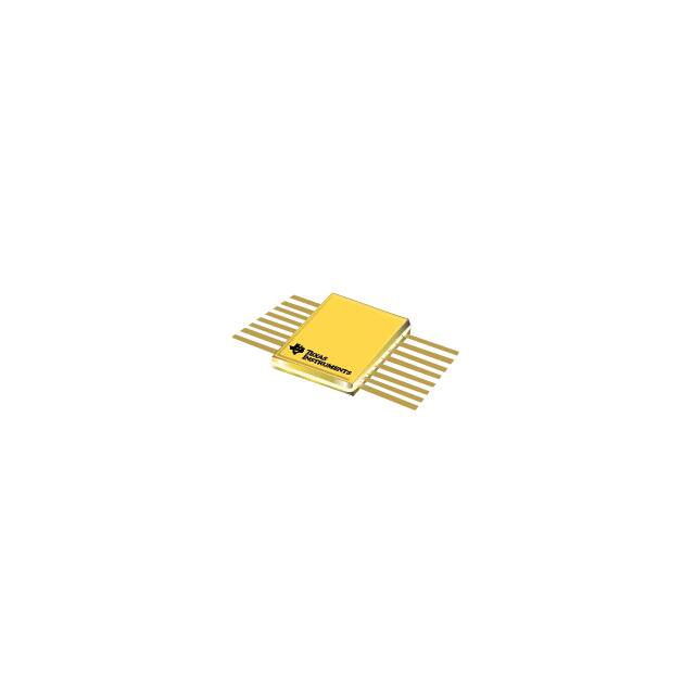
Thermally-enhanced CFP package, 0.4° C/W RθJC
2 Applications
•
•
•
•
•
•
•
Space satellite point of load supply for FPGAs,
microcontrollers, ASICs, and data converters
Radiation-hardened low-noise linear regulator
power supply for RF, VCOs, receivers, and
amplifiers
Clean analog supply requirements
Command and data handling (C&DH)
Optical imaging payload
Radar imaging payload
Satellite electrical power system (EPS)
PMOS pass element configuration. It operates over
a wide range of input voltage, from 1.5 V to 7 V
while offering excellent PSRR. The TPS7H1101A-SP
features a precise and programmable foldback current
limit implementation with a very-wide adjustment
range. To support the complex power requirements of
FPGAs, DSPs, or microcontrollers, the TPS7H1101ASP provides enable on and off functionality,
programmable soft start, current sharing capability,
and a Power Good open-drain output.
Device Information
PART NUMBER(1)
GRADE
5962R1320202V9A
KGD Flight Grade
RHA 100 krad(Si)
5962R1320202VXC
Flight Grade RHA
100 krad(Si)
TPS7H1101HKR/EM
Engineering
Modules(3) (5)
TPS7H1101AHKR/EM
Engineering
Modules(3)
TPS7H1101SPEVM
Ceramic
Evaluation Board
(1)
(2)
(3)
(4)
(5)
PACKAGE
16-Pin CFP
9.60 mm × 11.00 mm
Weight: 1.55 g(4)
EVM
For all available packages, see the orderable addendum at
the end of the data sheet.
See Radiation Report (SNAA257) for details.
These units are intended for engineering evaluation only.
They are processed to a noncompliant flow (that is, no
burn-in, and so forth) and are tested to a temperature
rating of 25°C only. These units are not suitable for
qualification, production, radiation testing or flight use. Parts
are not warranted for performance over the full MIL specified
temperature range of –55°C to 125°C or operating life.
Weight is accurate to ±10%.
TPS7H1101HKR/EM with device Date Code newer than 1705
is equivalent to TPS7H1101AHKR/EM using rev A silicon.
TPS7H1101A-SP
Power
Good
5V
VIN
CIN
RCS
COMP
EN
RT
PCL
Soft
Start
RPCL
CSS
3.3 V
VOUT
CS
GND
COUT
Feed
Back
RB
Copyright © 2017, Texas Instruments Incorporated
Typical Application Circuit
3 Description
The TPS7H1101A-SP is an improved version of
the TPS7H1101-SP allowing the use of the enable
feature across the entire input voltage range. It is a
radiation-hardened LDO linear regulator that uses a
An©IMPORTANT
NOTICEIncorporated
at the end of this data sheet addresses availability, warranty, changes, use in
safety-critical
applications,
Copyright
2021 Texas Instruments
Submit
Document
Feedback
intellectual property matters and other important disclaimers. PRODUCTION DATA.
Product Folder Links: TPS7H1101A-SP
1
�TPS7H1101A-SP
www.ti.com
SLVSDW6C – APRIL 2017 – REVISED APRIL 2021
Table of Contents
1 Features............................................................................1
2 Applications..................................................................... 1
3 Description.......................................................................1
4 Revision History.............................................................. 2
5 Pin Configuration and Functions...................................3
6 Specifications.................................................................. 6
6.1 Absolute Maximum Ratings........................................ 6
6.2 ESD Ratings............................................................... 6
6.3 Recommended Operating Conditions.........................6
6.4 Thermal Information....................................................6
6.5 Electrical Characteristics.............................................7
6.6 Typical Characteristics.............................................. 10
7 Detailed Description......................................................12
7.1 Overview................................................................... 12
7.2 Functional Block Diagram......................................... 12
7.3 Feature Description...................................................13
7.4 Device Functional Modes..........................................13
8 Application and Implementation.................................. 14
8.1 Application Information............................................. 14
8.2 Typical Application.................................................... 15
9 Power Supply Recommendations................................26
10 Layout...........................................................................26
10.1 Layout Guidelines................................................... 26
10.2 Layout Example...................................................... 26
11 Device and Documentation Support..........................27
11.1 Device Support........................................................27
11.2 Documentation Support.......................................... 27
11.3 Receiving Notification of Documentation Updates.. 27
11.4 Support Resources................................................. 27
11.5 Trademarks............................................................. 27
11.6 Electrostatic Discharge Caution.............................. 27
11.7 Glossary.................................................................. 27
12 Mechanical, Packaging, and Orderable
Information.................................................................... 27
4 Revision History
NOTE: Page numbers for previous revisions may differ from page numbers in the current version.
Changes from Revision B (June 2020) to Revision C (April 2021)
Page
• Updated the numbering format for tables, figures, and cross-references throughout the document..................1
• Added TPS7H1101AHKR/EM to Device Information table.................................................................................1
Changes from Revision A (August 2017) to Revision B (June 2020)
Page
• Added package weight to Device Information table............................................................................................1
• Added note to Pin Functions table for thermal pad and lid................................................................................. 3
• Added updated thermal metrics in Thermal Information table............................................................................ 6
• Changed and relaxed VCS operating range........................................................................................................ 7
• Added table note for VCS ................................................................................................................................... 7
• Changed CSR ratio. Added limits by temperature .............................................................................................7
• Added clarification for TEN ................................................................................................................................. 7
• Changed Overview section for improved clarity .............................................................................................. 12
• Changed and clarifed VREF voltage in CSS calculation .................................................................................... 13
• Changed Stability applications section............................................................................................................. 14
• Changed and corrected PCL section description............................................................................................. 16
• Changed and clarified High-Side Current Sense section description .............................................................. 17
• Changed and clarified Current Foldback section description........................................................................... 19
• Changed and improved Layout Example section............................................................................................. 26
Changes from Revision * (April 2017) to Revision A (August 2017)
Page
• Added Bare Die Information table.......................................................................................................................3
• Added Bond Pad Coordinates in Microns table.................................................................................................. 3
2
Submit Document Feedback
Copyright © 2021 Texas Instruments Incorporated
Product Folder Links: TPS7H1101A-SP
�TPS7H1101A-SP
www.ti.com
SLVSDW6C – APRIL 2017 – REVISED APRIL 2021
5 Pin Configuration and Functions
SS
1
16
FB
EN
2
15
COMP
VIN
3
14
VOUT
VIN
4
13
VOUT
12
VOUT
Thermal
VIN
5
VIN
6
11
VOUT
PCL
7
10
CS
GND
8
9
Pad
PG/OC
Not to scale
Figure 5-1. HKR Package
16-Pin CFP
Bottom View
Table 5-1. Pin Functions
PIN
NAME
NO.
I/O
DESCRIPTION
Soft-start terminal. Connecting an external capacitor slows down the output voltage ramp rate after enable
event.
SS
1
I/O
EN
2
I
Enable terminal. Driving this terminal to logic high enables the device; driving the terminal to logic low
disables the device.
I
Unregulated supply voltage. TI recommends to connect an input capacitor as a good analog circuit practice.
3
4
VIN
5
6
PCL
7
I/O
Programmable current limit. A resistor to GND sets the overcurrent limit activation point.
The range of resistor that can be used on the PCL terminal to GND is 8.2 kΩ to 160 kΩ.
GND
8
—
Ground/thermal pad.(1) (2)
PG/OC
9
O
Power Good terminal. PG is an open-drain output to indicate the output voltage reaches 90% of target. PG
terminal is also used as indicator when an overcurrent condition is activated. PG pin should have a pull-up
resistor to the VOUT pin.
I/O
Current sense terminal. Resistor connected from CS to VIN. CS terminal indicates voltage proportional to
output current.
CS terminal low: Foldback current limit disabled.
CS terminal high: Foldback current limit enabled.
O
Regulated output.
Internal compensation point for error amplifier.
CS
10
11
12
VOUT
13
14
COMP
15
I/O
FB
16
I
(1)
(2)
The output voltage feedback input through voltage dividers. See Section 8.2.1.1.
Thermal pad must be connected to GND.
Thermal pad and package lid are internally connected to GND.
Submit Document Feedback
Copyright © 2021 Texas Instruments Incorporated
Product Folder Links: TPS7H1101A-SP
3
�TPS7H1101A-SP
www.ti.com
SLVSDW6C – APRIL 2017 – REVISED APRIL 2021
Table 5-2. Bare Die Information
DIE THICKNESS
BACKSIDE FINISH
BACKSIDE
POTENTIAL
BOND PAD
METALLIZATION COMPOSITION
BOND PAD THICKNESS
15 mils
Silicon with backgrind
Ground
AlCu
30 kA
All dimensions are in microns.
4
Submit Document Feedback
Copyright © 2021 Texas Instruments Incorporated
Product Folder Links: TPS7H1101A-SP
�TPS7H1101A-SP
www.ti.com
SLVSDW6C – APRIL 2017 – REVISED APRIL 2021
Table 5-3. Bond Pad Coordinates in Microns
DESCRIPTION
PAD NUMBER
X MIN
Y MIN
X MAX
Y MAX
SS
1
109.89
4046.805
287.19
4224.105
EN
2
109.89
3493.35
287.19
3670.65
VIN
3
1359.99
3021.345
1537.29
3198.645
VIN
4
1359.99
2749.005
1537.29
2926.305
VIN
5
1359.99
2553.705
1537.29
2731.005
VIN
6
1359.99
2281.365
1537.29
2458.665
VIN
7
1359.99
2086.065
1537.29
2263.365
VIN
8
1359.99
1813.725
1537.29
1991.025
VIN
9
1359.99
1618.425
1537.29
1795.725
PCL
10
109.89
660.285
287.19
837.585
GND
11
109.89
319.455
287.19
496.755
GND
12
392.58
109.935
569.88
287.235
VIN
13
1359.99
1346.085
1537.29
1523.385
PG/OC
14
2898.945
379.62
3076.245
556.92
CS
15
2898.945
724.32
3076.245
901.62
VOUT
16
2829.105
1384.695
3006.405
1561.995
VOUT
17
2829.105
1579.815
3006.405
1757.115
VOUT
18
2829.105
1852.335
3006.405
2029.635
VOUT
19
2829.105
2047.455
3006.405
2224.755
VOUT
20
2829.105
2319.975
3006.405
2497.275
VOUT
21
2829.105
2515.095
3006.405
2692.395
VOUT
22
2829.105
2787.615
3006.405
2964.915
VOUT
23
2829.105
2982.735
3006.405
3160.035
COMP
24
2898.945
3519.72
3076.245
3697.02
FB
25
2898.945
3956.535
3076.245
4133.835
Submit Document Feedback
Copyright © 2021 Texas Instruments Incorporated
Product Folder Links: TPS7H1101A-SP
5
�TPS7H1101A-SP
www.ti.com
SLVSDW6C – APRIL 2017 – REVISED APRIL 2021
6 Specifications
6.1 Absolute Maximum Ratings
over operating free-air temperature range (unless otherwise noted) (1)
Input voltage
Output voltage
MIN
MAX
VIN, PG
–0.3
7.5
FB, COMP, PCL, CS, EN
–0.3
VIN + 0.3
VOUT, SS
–0.3
7.5
V
PG terminal sink current
UNIT
V
0.001
5
mA
Maximum operating junction temperature, TJ
–55
150
°C
Storage temperature, Tstg
–55
150
°C
(1)
Stresses beyond those listed under Absolute Maximum Ratings may cause permanent damage to the device. These are stress
ratings only, which do not imply functional operation of the device at these or any other conditions beyond those indicated under
Recommended Operating Conditions. Exposure to absolute-maximum-rated conditions for extended periods may affect device
reliability.
6.2 ESD Ratings
VALUE
V(ESD)
(1)
(2)
Electrostatic discharge
Human-body model (HBM), per ANSI/ESDA/JEDEC JS-001, all pins(1)
±2000
Charged-device model (CDM), per JEDEC specification JESD22-C101, all pins(2)
±1000
UNIT
V
JEDEC document JEP155 states that 500-V HBM allows safe manufacturing with a standard ESD control process.
JEDEC document JEP157 states that 250-V CDM allows safe manufacturing with a standard ESD control process.
6.3 Recommended Operating Conditions
over operating free-air temperature range (unless otherwise noted)
MIN
TJ
Operating junction temperature
NOM
–55
MAX
UNIT
125
°C
6.4 Thermal Information
TPS7H1101A-SP
THERMAL
METRIC(1) (2) (3)
HKR (CFP)
UNIT
16 PINS
Rθ JA
Junction-to-ambient thermal resistance
24.3
°C/W
Rθ JC(top)
Junction-to-case (top) thermal resistance
5.5
°C/W
Rθ JB
Junction-to-board thermal resistance
8.1
°C/W
ψJT
Junction-to-top characterization parameter
1.3
°C/W
ψJB
Junction-to-board characterization parameter
8.1
°C/W
RθJC(bot)
Junction-to-case (bottom) thermal resistance
0.4
°C/W
(1)
(2)
(3)
6
For more information about traditional and new thermal metrics, see the Semiconductor and IC Package Thermal Metrics application
report, SPRA953.
Do not allow package body temperature to exceed 265°C at any time or permanent damage may result.
Maximum power dissipation may be limited by overcurrent protection.
Submit Document Feedback
Copyright © 2021 Texas Instruments Incorporated
Product Folder Links: TPS7H1101A-SP
�TPS7H1101A-SP
www.ti.com
SLVSDW6C – APRIL 2017 – REVISED APRIL 2021
6.5 Electrical Characteristics
1.5 V ≤ VIN ≤ 7 V, VOUT(target) = VIN – 0.35 V, IOUT = 10 mA, VEN = 1.1 V, COUT = 22 µF, PG terminal pulled up to VIN with
50 kΩ, over operating temperature range (TJ = –55°C to 125°C), unless otherwise noted. Typical values are at TJ = 25°C.
PARAMETER
VIN
TEST CONDITIONS
Input voltage range
voltage(1)
VFB
Feedback terminal
VOUT
Output voltage range
0 A ≤ IOUT ≤ 3 A, 1.5 V ≤ VIN ≤ 7 V
0 A ≤ IOUT ≤ 3 A, 1.5 V ≤ VIN ≤ 7 V,
VOUT = 0.8 V, 1.2 V, 1.8 V, 6.65 V
ΔVOUT%/
ΔVIN
Line regulation
1.5 V ≤ VIN ≤ 7 V
ΔVOUT%/
ΔIOUT
Load regulation
0.8 V ≤ VOUT ≤ 6.65 V, 0 ≤ ILoad ≤ 3 A
DC input line regulation
TYP
1.5
Output voltage accuracy(1)
ΔVOUT
MIN
0.594
MAX
7
V
0.616
V
0.8
VIN
V
–2%
2%
–0.07
0.605
UNIT
0.01
0.07
0.08
%/V
%/A
1.5 V ≤ VIN ≤ 7 V, VOUT = 0.8 V, 1.2 V, 1.8 V,
IOUT = 10 mA, TJ = –55°C(2)
0.5
3
1.5 V ≤ VIN ≤ 7 V, VOUT = 0.8 V, 1.2 V, 1.8 V,
IOUT = 10 mA, TJ = 25°C(2)
0.2
0.6
1.5 V ≤ VIN ≤ 7 V, VOUT = 0.8 V, 1.2 V, 1.8 V,
IOUT = 10 mA, TJ = 125°C(2)
0.2
1
mV
Submit Document Feedback
Copyright © 2021 Texas Instruments Incorporated
Product Folder Links: TPS7H1101A-SP
7
�TPS7H1101A-SP
www.ti.com
SLVSDW6C – APRIL 2017 – REVISED APRIL 2021
6.5 Electrical Characteristics (continued)
1.5 V ≤ VIN ≤ 7 V, VOUT(target) = VIN – 0.35 V, IOUT = 10 mA, VEN = 1.1 V, COUT = 22 µF, PG terminal pulled up to VIN with
50 kΩ, over operating temperature range (TJ = –55°C to 125°C), unless otherwise noted. Typical values are at TJ = 25°C.
PARAMETER
TYP
MAX
VOUT = 0.8 V, 0 ≤ ILoad ≤ 1 A, TJ = –55°C(2)
TEST CONDITIONS
0.4
1
VOUT = 0.8 V, 0 ≤ ILoad ≤ 1 A, TJ = 25°C(2)
0.6
1.1
VOUT = 0.8 V, 0 ≤ ILoad ≤ 1 A, TJ = 125°C(2)
0.8
1.3
–55°C(2)
VOUT = 0.8 V, 0 ≤ ILoad ≤ 2 A, TJ =
MIN
0.8
1.8
VOUT = 0.8 V, 0 ≤ ILoad ≤ 2 A, TJ = 25°C(2)
1.3
1.8
VOUT = 0.8 V, 0 ≤ ILoad ≤ 2 A, TJ = 125°C(2)
1.6
2.4
–55°C(2)
1.1
1.9
1.9
2.6
125°C(2)
2.5
3.4
VOUT = 1.2 V, 0 ≤ ILoad ≤ 1 A, TJ = –55°C(2)
0.3
1.2
VOUT = 0.8 V, 0 ≤ ILoad ≤ 3 A, TJ =
VOUT = 0.8 V, 0 ≤ ILoad ≤ 3 A, TJ = 25°C(2)
VOUT = 0.8 V, 0 ≤ ILoad ≤ 3 A, TJ =
VOUT = 1.2 V, 0 ≤ ILoad ≤ 1 A, TJ =
25°C(2)
0.5
1.3
VOUT = 1.2 V, 0 ≤ ILoad ≤ 1 A, TJ = 125°C(2)
0.6
1.3
–55°C(2)
0.8
1.6
1.1
2.1
125°C(2)
1.5
2.1
VOUT = 1.2 V, 0 ≤ ILoad ≤ 3 A, TJ = –55°C(2)
1
1.7
VOUT = 1.2 V, 0 ≤ ILoad ≤ 2 A, TJ =
VOUT = 1.2 V, 0 ≤ ILoad ≤ 2 A, TJ = 25°C(2)
VOUT = 1.2 V, 0 ≤ ILoad ≤ 2 A, TJ =
VOUT = 1.2 V, 0 ≤ ILoad ≤ 3 A, TJ =
ΔVO
DC output load regulation(3)
25°C(2)
1.1
2.4
VOUT = 1.2 V, 0 ≤ ILoad ≤ 3 A, TJ = 125°C(2)
2.2
3.5
–55°C(2)
0.1
0.9
VOUT = 1.8 V, 0 ≤ ILoad ≤ 1 A, TJ =
VOUT = 1.8 V, 0 ≤ ILoad ≤ 1 A, TJ = 25°C(2)
0.3
0.9
125°C(2)
0.4
1.2
VOUT = 1.8 V, 0 ≤ ILoad ≤ 2 A, TJ = –55°C(2)
1.4
2.4
VOUT = 1.8 V, 0 ≤ ILoad ≤ 1 A, TJ =
VOUT = 1.8 V, 0 ≤ ILoad ≤ 2 A, TJ =
25°C(2)
0.7
1.4
VOUT = 1.8 V, 0 ≤ ILoad ≤ 2 A, TJ = 125°C(2)
0.6
1.9
–55°C(2)
2.5
3.9
1.2
2.1
1.2
2.5
1.5
2.9
VOUT = 1.8 V, 0 ≤ ILoad ≤ 3 A, TJ =
VOUT = 1.8 V, 0 ≤ ILoad ≤ 3 A, TJ = 25°C(2)
VOUT = 1.8 V, 0 ≤ ILoad ≤ 3 A, TJ =
125°C(2)
VOUT = 6.65 V, 0 ≤ ILoad ≤ 1 A, TJ = –55°C(2)
VOUT = 6.65 V, 0 ≤ ILoad ≤ 1 A, TJ =
25°C(2)
0.4
2.6
VOUT = 6.65 V, 0 ≤ ILoad ≤ 1 A, TJ = 125°C(2)
2.8
3.5
–55°C(2)
3.5
5.9
1.1
4.7
VOUT = 6.65 V, 0 ≤ ILoad ≤ 2 A, TJ =
VOUT = 6.65 V, 0 ≤ ILoad ≤ 2 A, TJ = 25°C(2)
125°C(2)
5.8
8
VOUT = 6.65 V, 0 ≤ ILoad ≤ 3 A, TJ = –55°C(2)
5.6
9.3
VOUT = 6.65 V, 0 ≤ ILoad ≤ 3 A, TJ = 25°C(2)
3.7
8
VOUT = 6.65 V, 0 ≤ ILoad ≤ 3 A, TJ = 125°C(2)
13
25
IOUT = 3 A, VOUT = 1.3 V, VIN = VOUT + VDO
210
335
VOUT = 6.65 V, 0 ≤ ILoad ≤ 2 A, TJ =
VDO
Dropout voltage(3)
ICL
VIN = 1.5 V, VOUT = 1.2 V,
Programmable output current PCL resistance = 47 kΩ
limit range
VIN = 1.5 V, VOUT = 1.2 V,
PCL resistance varies
VCS
8
Operating voltage range at
CS (see Section 7)(5)
Submit Document Feedback
500
750
200
3500(4)
0
VIN
UNIT
mV
mV
mA
V
Copyright © 2021 Texas Instruments Incorporated
Product Folder Links: TPS7H1101A-SP
�TPS7H1101A-SP
www.ti.com
SLVSDW6C – APRIL 2017 – REVISED APRIL 2021
6.5 Electrical Characteristics (continued)
1.5 V ≤ VIN ≤ 7 V, VOUT(target) = VIN – 0.35 V, IOUT = 10 mA, VEN = 1.1 V, COUT = 22 µF, PG terminal pulled up to VIN with
50 kΩ, over operating temperature range (TJ = –55°C to 125°C), unless otherwise noted. Typical values are at TJ = 25°C.
PARAMETER
CSR
Current sense ratio
MIN
TYP
MAX
ILOAD / ICS, VIN = 2.3 V, VOUT = 1.9 V, TJ =
–55°C, ILOAD ≥ 500 mA
TEST CONDITIONS
45000
55500
65000
LOAD
/ ICS, VIN = 2.3 V, VOUT = 1.9 V, TJ =
25°C, ILOAD ≥ 500 mA
45000
52000
59000
/ ICS, VIN = 2.3 V, VOUT = 1.9 V, TJ =
125°C, ILOAD≥ 500 mA
45000
51000
56000
10
16
mA
7
10
mA
26
230
µA
1
5
nA
20
150
nA
0.55
V
LOAD
IGND
GND terminal current
VIN = 1.5 V, VOUT = 1.2 V, IOUT = 2 A
IQ
Quiescent current (no load)
VIN = VOUT + 0.5 V, IOUT = 0 A
ISHDN
Shutdown current
1.5 V ≤ VIN ≤ 7 V, pre and post 100 krad(Si),
TJ = 25°C(6)
ISNS, IFB
FB/SNS terminal current
VIN = 7 V, VOUT = 6.65 V
IEN
EN terminal input current
VIN = 7 V, VEN = 7 V, VOUT = 6.65 V
VILEN
EN terminal input low
(disable)
1.5 V < VIN < 7 V
VIHEN
EN terminal input high
(enable)
1.5 V < VIN < 7 V
Eprop Dly
Enable terminal propagation
delay
VIN = 2.2 V, EN rise to IOUTrise
TEN
Enable terminal turn-on delay VIN = 2.2 V, VOUT = 1.8 V, ILOAD = 1 A,
(delay to PG assertion)
COUT = 220 µF, CSS = 2 nF
VTHPG
PG threshold
UNIT
A/A
VIN – 0.7
No load, 0.8 V ≤ VOUT ≤ 6.65 V
86%
V
650
1000
µs
1.4
1.6
ms
300
mV
90%
VTHPGHYS
PG hysteresis
1.5 V ≤ VIN ≤ 7 V
2%
VOL PG
PG terminal output low
IPG = 0 mA to –1 mA
120
ILKGPG
PG terminal leakage current
VOUT > VTHPG, VPG = 1.2 V
0.2
1.5
VOUT > VTHPG, VPG = 7 V
0.5
2.5
µA
ISS
SS terminal charge current
VIN = 1.5 V to 7 V
2.5
3.5
µA
ISSdisb
SS terminal disable current
VIN = 1.5 V to 7 V
5
10
µA
VSS
SS terminal voltage (device
enabled)(7)
VIN = 1.5 V to 7 V
1.232
V
VSSdisb
SS terminal low-level input
voltage to disable device
VIN = 1.5 V to 7 V
0.4
V
PSRR
Power-supply rejection ratio
VIN = 2.5 V, VOUT = 1.8 V,
COUT = 220 µF
VN
Output noise voltage
BW = 10 Hz to 100 kHz,
IOUT = 3 A, VIN = 2 V, VOUT = 1.8 V
TSD
Thermal shutdown
temperature
(1)
(2)
(3)
(4)
(5)
(6)
(7)
1 kHz
48
100 kHz
25
20.33
dB
µVRMS
185
°C
The output voltage accuracy of condition at IOUT = 2 A and IOUT = 3 A is specified by characterization, but not production tested.
Line and load regulations done under pulse condition for t < 10 ms.
The parameter is specified to the limit in characterization, but not production tested.
The maximum limit of the ICLparameter is specified to the limit in characterization, but not production tested.
To insure foldback is enabled, VCS must be > 0.9 · VFB.
This maximum limit applies to SMD 5962R13202 post 100-krad(Si) test at 25°C.
Any external pullup voltage should not exceed 1.188 V.
Submit Document Feedback
Copyright © 2021 Texas Instruments Incorporated
Product Folder Links: TPS7H1101A-SP
9
�TPS7H1101A-SP
www.ti.com
SLVSDW6C – APRIL 2017 – REVISED APRIL 2021
6.6 Typical Characteristics
0.608
10
Quiescent Current (mA)
Feedback Voltage (V)
0.607
0.606
0.605
VIN = 1.5 V
0.604
0.603
9
8
VIN = 7 V
7
VIN = 1.5 V
6
VIN = 7 V
0.602
-55
5
-35
-15
5
25
45
65
85
105
125
±55
±35
25
45
65
85
105
Junction Temperature (ƒC)
Figure 6-1. Feedback Voltage vs Temperature
125
C014
Figure 6-2. Quiescent Current vs Temperature
320
13
12
Load = 2 A
280
11
Dropout Voltage (mV)
Ground Current (mA)
5
±15
Junction Temperature (°C)
10
9
No Load
8
7
240
200
160
6
5
±55
±35
5
±15
25
45
65
85
105
Junction Temperature (ƒC)
125
120
-55
-35
C015
-15
5
25
45
65
Junction Temperature (°C)
VOUT = 1.8 V
125
Load = 3 A
100
100
80
95
VIN = 7 V
PG Threshold (%)
Shutdown Current (uA)
105
Figure 6-4. Dropout Voltage vs Temperature
Figure 6-3. Ground Current vs Temperature
60
40
VIN = 1.5 V
20
90
85
0
80
-55
-35
-15
5
25
45
65
85
105
Junction Temperature (°C)
125
-55
-35
-15
5
25
45
65
85
105
Junction Temperature (°C)
C017
Figure 6-5. Shutdown Current vs Temperature
10
85
125
C018
Figure 6-6. PG Threshold vs Temperature
Submit Document Feedback
Copyright © 2021 Texas Instruments Incorporated
Product Folder Links: TPS7H1101A-SP
�TPS7H1101A-SP
www.ti.com
SLVSDW6C – APRIL 2017 – REVISED APRIL 2021
6.6 Typical Characteristics (continued)
100
No load
1A
2A
3A
Ripple Rejection (dB)
80
60
40
20
0
10
100
1000
10000
100000
Frequency (Hz)
VIN = 2.5 V
VOUT = 1.8 V
Figure 6-7. Power Supply Ripple Rejection vs Frequency
Submit Document Feedback
Copyright © 2021 Texas Instruments Incorporated
Product Folder Links: TPS7H1101A-SP
11
�TPS7H1101A-SP
www.ti.com
SLVSDW6C – APRIL 2017 – REVISED APRIL 2021
7 Detailed Description
7.1 Overview
The TPS7H1101A-SP is 3-A, 1.5-V to 7-V LDO linear regulator that uses PMOS pass element configuration.
It uses TI’s proprietary process to achieve low noise, high PSRR combined with high-thermal performance in a
16-pin ceramic flatpack package (HKR).
A number of features are incorporated in the design to provide high reliability and system flexibility. Current
foldback, current limit, and thermal protection are incorporated in the design to make it viable for space
environments.
The device also has a current sense monitoring feature. A resistor connected from the current sense (CS)
terminal to VIN indicates voltage proportional to the output current. Section 8.2.1.3 provides a detailed
description of this feature. When CS is pulled high to voltage greater than 90% Vref (0.544 V), foldback current
limit is enabled. Pulling CS below 0.544 V disables the foldback current limit.
A resistor connected from the programmable current limit (PCL) terminal to ground sets the overcurrent limit
activation point. When overcurrent limit activation point is reached, it results in the LDO going into current
foldback mode. Output current is reduced to approximately 50% of the current limit set point. Section 8.2.1.2
provides a detailed description of this feature.
TPS7H1101A-SP incorporates thermal protection, which disables the output when the junction temperature rises
to approximately 185°C, allowing the device to cool. Cycling limits the dissipation of the regulator, protecting it
from catastrophic damage as a result of overheating.
To provide system flexibility for demanding current needs, the LDO can be configured in parallel operation as
indicated in Figure 8-12. Section 8.2.1.6 provides detailed parallel operation information.
An enable feature is incorporated in the design allowing the user to enable or disable the LDO. Power
Good (PG), is an open-drain connection, indicating status of the output voltage regulation. These provide the
customers system flexibility in monitoring and controlling the LDO operation.
7.2 Functional Block Diagram
CS
VIN
1.2 V
2 mA
EN
ISS
Thermal
Protection
OCP
RTOP
PCL
RBOT
VREF
1.1*VREF
PG
0.9*VREF
12
Submit Document Feedback
Copyright © 2021 Texas Instruments Incorporated
Product Folder Links: TPS7H1101A-SP
�TPS7H1101A-SP
www.ti.com
SLVSDW6C – APRIL 2017 – REVISED APRIL 2021
7.3 Feature Description
7.3.1 Soft Start
Connecting a capacitor (CSS) from the SS terminal to GND slows down the output voltage ramp rate. The
soft-start capacitor charges up to 1.2 V, with a threshold of VFB.
tSS · ISS
CSS = ¾
VFB
(1)
where
•
•
•
tss = soft-start time
Iss = 2.5 µA
VFB = VREF = 0.605 V
7.3.2 Power Good (PG)
Power Good terminal (9) is an open-drain connection and can be used to sequence multiple LDOs. Figure
7-1 shows typical connection. The PG terminal will be pulled low until the output voltage reaches 90% of its
maximum level. At that point, the PG pin will be pulled up. Since the PG pin is open drain, it can be pulled up to
any voltage as long as it does not exceed the absolute max of 7.5 V listed in Section 6.5.
TPS7H1101A-SP
EN
TPS7H1101A-SP
PG
SS
VIN
EN
PG
VIN
SS
Copyright © 2017, Texas Instruments Incorporated
Figure 7-1. Sequencing LDOs With Power Good
Note
For PSpice models, WEBENCH, and reference design, see the Design & development tab of the
product folder.
1. PSpice transient model (switching, transient, and stability simulations)
2. PSpice Worst Case Analysis (WCA) model (radiation and aging stability – Bode plot)
7.4 Device Functional Modes
7.4.1 Enable/Disable
For VIN from 1.5 V to 7 V, TPS7H1101A-SP can be disabled by pulling the enable terminal to logic low at a
minimum of 0.7 V. Enable cannot exceed VIN by more than 0.3 V, and in most cases, the enable terminal is
connected to VIN.
Submit Document Feedback
Copyright © 2021 Texas Instruments Incorporated
Product Folder Links: TPS7H1101A-SP
13
�TPS7H1101A-SP
www.ti.com
SLVSDW6C – APRIL 2017 – REVISED APRIL 2021
8 Application and Implementation
Note
Information in the following applications sections is not part of the TI component specification,
and TI does not warrant its accuracy or completeness. TI’s customers are responsible for
determining suitability of components for their purposes, as well as validating and testing their design
implementation to confirm system functionality.
8.1 Application Information
The TPS7H1101A-SP LDO linear regulator is targeted space environment applications. This regulator has
various features such as low dropout, soft start, output current foldback, high-side current sensing (where
sensing voltage at CS pin provides voltage proportional to output current), and current sharing.
8.1.1 Stability
Bode plots are a standard approach in assessing stability. This approach requires a single feedback path
where an AC signal is injected across a resistor (typically 50 Ω) and measurements are taken on either side
of the resistor as shown in Figure 8-1. From this measurement, loop gain and phase plots can be generated.
Crossover frequency, ƒC, is defined as the frequency where the magnitude of the loop gain is unity and phase
margin is evaluated at the crossover frequency ƒC.
Signal
injection
TPS7H1101A-SP
IN
OUT
50Ÿ
VIN
+
±
RESR
RESR
CCOMP
gm
COMP
RLOAD
RT
COUT
CIN
FB
RB
0.6V VREF
Figure 8-1. Conventional Bode Plot With Simplified Feedback Loops
However, it is important the AC signal is injected as shown in Figure 8-1. This injection point ensures that the
feedback signal goes through both the outer loop (consisting of the top feedback resistor, RT) and the inner loop
(consisting of the compensation capacitor, CCOMP). If the only the outer loop is measured, the resulting crossover
frequency will be lower which would indicate a poorer transient response than reality. Therefore, it is best to
inject the measurement signal at a point where it goes through both loops. If this is not possible, the two loops
may be measured independently and added using the superposition principle.
Furthermore, the stability of the device can be qualitatively validated by applying a step load to the output and
observing the response. The SPICE models for the device can be found on the TPS7H1101A-SP product page.
To simulate impedance measurements, the transient model should be used.
14
Submit Document Feedback
Copyright © 2021 Texas Instruments Incorporated
Product Folder Links: TPS7H1101A-SP
�TPS7H1101A-SP
www.ti.com
SLVSDW6C – APRIL 2017 – REVISED APRIL 2021
8.2 Typical Application
TPS7H1101A-SP
Power
Good
5V
VIN
CIN
RCS
COMP
EN
RT
PCL
RPCL
Soft
Start
CSS
3.3 V
VOUT
CS
GND
COUT
Feed
Back
RB
Copyright © 2017, Texas Instruments Incorporated
Figure 8-2. Typical Application Circuit
Submit Document Feedback
Copyright © 2021 Texas Instruments Incorporated
Product Folder Links: TPS7H1101A-SP
15
�TPS7H1101A-SP
www.ti.com
SLVSDW6C – APRIL 2017 – REVISED APRIL 2021
8.2.1 Detailed Design Procedure
8.2.1.1 Adjustable Output Voltage (Feedback Circuit)
The output voltage of the TPS7H1101A-SP can be set to a user-programmable level between 0.8 V and 6.65
V. Achieve this by using a resistor divider connected between VOUT, FB, and GND terminals. RTOP connected
between VOUT and VFB, and RBOTTOM connected between VFB and GND.
Use Equation 2 to determine VOUT.
(RTOP + RBOTTOM) · VFB
VOUT = ¾
RBOTTOM
(2)
where
•
VFB = 0.605 V
Table 8-1. Example Resistor Values for Typical
Voltages
VOUT
Standard 1% Resistors
Standard 0.1% Resistors
RTOP
RBOTTOM
RTOP
RBOTTOM
0.8 V
10.7 kΩ
33.2 kΩ
10.7 kΩ
33.2 kΩ
1V
13.7 kΩ
21 kΩ
12.6 kΩ
19.3 kΩ
1.2 V
11.3 kΩ
11.5 kΩ
11.8 kΩ
12 kΩ
1.5 V
15.8 kΩ
10.7 kΩ
18.2 kΩ
12.3 kΩ
1.8 V
23.2 kΩ
11.8 kΩ
32 kΩ
16.2 kΩ
2.5 V
10.7 kΩ
3.4 kΩ
37.9 kΩ
12.1 kΩ
3.3 V
51.1 kΩ
11.5 kΩ
10.2 kΩ
2.29 kΩ
4V
13.3 kΩ
2.37 kΩ
31.2 kΩ
5.56 kΩ
5V
11.5 kΩ
1.58 kΩ
16.2 kΩ
2.23 kΩ
5.5 V
17.4 kΩ
2.15 kΩ
89.8 kΩ
11.1 kΩ
6V
90.9 kΩ
10.2 kΩ
10.7 kΩ
1.2 kΩ
6.5 V
26.7 kΩ
2.74 kΩ
15.2 kΩ
1.56 kΩ
6.6 V
11.3 kΩ
1.15 kΩ
22.1 kΩ
2.23 kΩ
6.7 V
39.2 kΩ
3.92 kΩ
13.8 kΩ
1.37 kΩ
8.2.1.2 PCL
PCL resistor, RPCL, sets the overcurrent limit activation point and can be calculated per Equation 3.
RPCL = (CSR × VREF) / (ICL – 0.0403)
(3)
where
•
•
•
•
VREF = 0.605 V
ICL = Programmable current limit (A)
Current sense ratio (CSR) is the ratio of output load current to ICS; typical value of the CSR is 52000
Offset value 0.0403 is a fixed offset derived from internal keep-alive biasing
Figure 8-3 shows the output load current (ILOAD) versus PCL terminal current (IPCL) varied with minimum and
maximum range of CSR values by temperature. The RPCL resistor should be chosen to set the worst case ILOAD
across system normal operating load and temperature range without reaching overcurrent activation point of IPCL
· RPCL ≥ VREF.
Additionally, a suitable resistor RCS must be chosen to ensure the CS terminal is within its operating range of 0.3
V to VIN and VCS needs to be greater than 0.9 · VREF (0.544 V) to insure foldback remains enabled when current
activation point is triggered.
16
Submit Document Feedback
Copyright © 2021 Texas Instruments Incorporated
Product Folder Links: TPS7H1101A-SP
�TPS7H1101A-SP
www.ti.com
SLVSDW6C – APRIL 2017 – REVISED APRIL 2021
The maximum PCL is 3.5 A. The range of resistor that can be used on the PCL terminal to GND is 8.2 kΩ to 160
kΩ. It is not recommended to use overcurrent limit activation thresholds of less than 500 mA due to internal bias
offset currents representing a larger percentage of total IPCLcurrent and therefore additional error.
ILOAD Vs IPCL across CSR range
6
5
Min CSR: ILOAD = 45000 * IPCL +0.0403
25c Nom CSR: ILOAD = 52000 * IPCL +0.0403
125c Max CSR: ILOAD = 56000 * IPCL +0.0403
-55c Max CSR: ILOAD = 65000 * IPCL +0.0403
ILOAD (A)
4
3
2
1
0
0x100
10x10-6
20x10-6
30x10-6
40x10-6
50x10-6
60x10-6
70x10-6
IPCL (A)
80x10-6
CSR_
Figure 8-3. ILOAD (A) vs IPCL (A)
8.2.1.3 High-Side Current Sense
Figure 8-4 shows the cascode NMOS current mirror. VCS must be ≥ 0.3 V for proper biasing. Additionally VCS
must be greater than 0.9 · VREF (0.544 V) if foldback current limiting is intended to be enabled. The following
example shows the typical calculation of RCS.
I CS =
I LOAD + I offset
(4)
CSR
VIN - VCS
RCS = ¾¾
ICS
(5)
where
•
•
•
•
ILOAD is the output load current
CSR is the current sense ratio
Ioffset is internal keep-alive bias current times CSR
Ioffset = 5 µA · CSR
When VIN = 2.3 V, select VCS = 2.05 V, ILOAD = 3 A, CSR = 52000, and Ioffset = 0.26 A, then ICS = 62.69 µA and
RCS = 3.99 kΩ.
Submit Document Feedback
Copyright © 2021 Texas Instruments Incorporated
Product Folder Links: TPS7H1101A-SP
17
�TPS7H1101A-SP
www.ti.com
SLVSDW6C – APRIL 2017 – REVISED APRIL 2021
Vin
Iout
Ics
Rcs
Vcs
Vcs
Figure 8-4. Cascode NMOS Current Mirror
For TPS7H1101A-SP, Figure 8-5 shows a typical curve VCS vs IOUT for VIN = 2.28 V and RCS = 3.65 kΩ. A
resistor connected from the CS terminal to VIN indicates voltage proportional to the output current.
Monitoring current in the CS terminal (ICS vs ILOAD) indicates the current sense ratio between the main
PMOSFET and the current sense MOSFET as shown in Figure 8-6. Additionally Figure 8-6 shows the linearity
of the CSR ratio across VCS pin voltage range of 0.3 V to VIN. VCS must be ≥ 0.3-V minimum to keep circuit
properly biased.
2.35
3.5
2.30
3
2.25
2.5
2.20
ILOAD (A)
CS Pin Voltage (V)
Figure 8-7 shows ILOAD vs ICS across the full range of CSR values.
2.15
2.10
ICS (uA) vs ILOAD at VCS = 0.3V
ICS (uA) vs ILOAD at VCS = 2.3V
ICS (uA) vs ILOAD at VCS = 5V
2
1.5
1
2.05
0.5
2.00
0.0
0.5
1.0
1.5
2.0
2.5
3.0
Load Current (A)
VIN = 2.3 V
VOUT = 1.8 V
4.0
0
0
10
y = –0.078x + 2.2853
20
30
40
50
60
ICS (uA)
C003
Figure 8-5. VCS (V) vs I LOAD (A)
18
3.5
VIN = 2.3 V
70
80
VCS_
VOUT = 1.8 V
Figure 8-6. IOUT (A) vs ICS (A)
Submit Document Feedback
Copyright © 2021 Texas Instruments Incorporated
Product Folder Links: TPS7H1101A-SP
�TPS7H1101A-SP
www.ti.com
SLVSDW6C – APRIL 2017 – REVISED APRIL 2021
ILOAD Vs ICS across CSR range
6
5
Min CSR: ILOAD = 45000(ICS - 5uA)
25c Nom CSR: ILOAD = 52000(ICS - 5uA)
-55c Max CSR: ILOAD = 65000(ICS - 5uA)
125c Max CSR: ILOAD = 56000(ICS - 5uA)
ILOAD (A)
4
3
2
1
0
0x100
10x10-6
20x10-6
30x10-6
40x10-6
50x10-6
60x10-6
70x10-6
ICS (A)
80x10-6
CSR_
Figure 8-7. IOUT (A) vs ICS (A)
8.2.1.4 Current Foldback
1. The TPS7H1101A-SP has a current foldback feature which can be enabled when the CS terminal is greater
than 0.9 · VREF (0.544 V). Pulling CS below this threshold disables the foldback current limit. If the foldback
current limit is disabled, then the LDO will begin regulating again as soon as the current falls below the
clamp threshold.
2. With foldback current limit enabled, when current limit trip point is activated,
a. Output voltage drops low, and
b. Output current folds back to approximately 50% of the current limit trip point.
This results in minimizing the power loss under fault conditions. Monitoring the voltage at the CS terminal
indicates voltage proportional to the output current. It is important to note that the current sense voltage
range on CS pin must be designed to stay above the 0.9 · VREF threshold to insure foldback is not
inadvertently disabled at high currents.
Submit Document Feedback
Copyright © 2021 Texas Instruments Incorporated
Product Folder Links: TPS7H1101A-SP
19
�TPS7H1101A-SP
www.ti.com
SLVSDW6C – APRIL 2017 – REVISED APRIL 2021
8.2.1.5 Transient Response
Figure 8-8, Figure 8-9, and Figure 8-10 indicate the transient response behavior of the LDO for 50% step load
change.
Channel 1: Input voltage
Channel 3: Step load in current
Channel 4: Output voltage overshoot/undershoot
Figure 8-8. Load Transient Response: Step Load
0.1 to 1.6 A, VIN = 2.3 V, VOUT = 1.8 V
Figure 8-9. Expanded View Overshoot
Figure 8-10. Expanded View Undershoot
20
Submit Document Feedback
Copyright © 2021 Texas Instruments Incorporated
Product Folder Links: TPS7H1101A-SP
�TPS7H1101A-SP
www.ti.com
SLVSDW6C – APRIL 2017 – REVISED APRIL 2021
8.2.1.6 Current Sharing
For demanding load requirements, multiple LDOs can be paralleled as indicated in Figure 8-12. In parallel mode,
the CS terminal of LDO1 must be connected to the PCL terminal of LDO2 via a series resistor, RCL, and CS
terminal of LDO2 must be connected to PCL terminal of LDO1 via series resistor, RCL. The typical value of RCL
in parallel operation is 3.75 kΩ for current limit > 6 A. In parallel configuration, RCL (resistor from PCL to GND)
and RCS (resistor from CS terminal to VIN) must be left open (unpopulated). The RCL value must be selected so
that the operating condition of the CS terminal is maintained, as specified in Section 6.5. VCS must be greater
than 0.3 V to insure proper current sense operation. The current from PCL through RCL of LDO1 is determined
by the output load current of LDO2 divided by the CSR. Hence, the voltage at CS terminal of the LDO1 is 0.605
V – ((output load current of LDO2 + 0.2458) / CSR × RCL).
Alternately, it can also provide twice the output current to meet system needs. When using two LDOs in parallel
operation for higher output load current, use POL TPS50601-SP as an input source.
65.00
LDO1
LDO2
60.00
% of total Load
55.00
50.00
45.00
40.00
35.00
0
1
2
3
4
5
6
Output Current
Figure 8-11. LDO Current Share
Submit Document Feedback
Copyright © 2021 Texas Instruments Incorporated
Product Folder Links: TPS7H1101A-SP
21
�TPS7H1101A-SP
www.ti.com
SLVSDW6C – APRIL 2017 – REVISED APRIL 2021
RPG
Supply
Ccomp
PG
VIN
Comp
LDO1 VOUT
SS
FB PCL
CS
RTOP
COUT
CX
RCL
RCL
RLOAD
RBOT
RCL
Optional
Supply
VIN
CS
SS
FB
PCL
Comp
LDO1 VOUT
Ccomp
PG
RPG
CSS
Figure 8-12. Block Diagram (Parallel Operation)
22
Submit Document Feedback
Copyright © 2021 Texas Instruments Incorporated
Product Folder Links: TPS7H1101A-SP
�TPS7H1101A-SP
www.ti.com
SLVSDW6C – APRIL 2017 – REVISED APRIL 2021
8.2.1.7 Compensation
Figure 8-13 shows a generic block diagram for TPS7H1101A-SP LDO with external compensation components.
LDO incorporates nested loops, thus providing the high gain necessary to meet design performance.
Q1
CCOMP
+
RINESR
Buffer
-
RTOP
RESR
E/A
VIN
CFF
RL
+
CO
CIN
VREF = 0.605 V
+
VOUT
-
RBOT
CX
Figure 8-13. TPS7H1101A-SP Compensation
Resistor divider composed of Rtop and Rbottom determine the output voltage set points as indicated by Equation
2.
Output capacitor COUT introduces a pole and a zero as shown in the following.
1
Fp_co = 2¾
·p·Co·RL
(6)
1
Fz_co = 2¾
·p·Co·Cesr
(7)
The TPS7H1101A-SP was designed so that the ESR of the output capacitor will not have a strong influence on
the response of the LDO. However, an optional capacitor, Cx, can be added in parallel with the bottom feedback
resistor to introduce a pole to cancel Fz_co. Equation 8 shows how to calculate the location of the pole introduced
by Cx. To cancel the zero directly, Fp should be equal to Fz_co.
1
Fp = 2¾
·p·Cx·Rbottom
(8)
Cx is calculated to be 1000 pF for Co = 220 µF, Cesr = 45 mΩ, and Rbottom = 10 kΩ.
Figure 8-13 also includes a place holder for a feed forward capacitance Cff. Use of feed forward compensation
can be more advantageous than use of Cx. Please reference application note Pros and Cons of Using a
Feedforward Capacitor with a Low-Dropout Regulator for additional information on usage of CFF.
Internal compensation in the LDO cancels the output capacitor pole introduced by COUT and RL.
Ccomp introduces a dominant pole at low frequency. TI recommends that a Ccomp value of 10 nF.
8.2.1.8 Output Noise
Output noise is measured using an HP3495A. Figure 8-14 and Figure 8-15 show noise of the TPS7H1101A-SP
in µV/√ Hz vs frequency.
Submit Document Feedback
Copyright © 2021 Texas Instruments Incorporated
Product Folder Links: TPS7H1101A-SP
23
�TPS7H1101A-SP
www.ti.com
10
10
1
1
Noise ( μ V/√Hz)
Noise (µV/√Hz)
SLVSDW6C – APRIL 2017 – REVISED APRIL 2021
0.1
0.1
0.01
10
100
1,000
10,000
100,000
0.01
10
100
Frequency (Hz)
VIN = 2 V
CIN = 220 µF
1000
10000
100000
Frequency (Hz)
VOUT = 1.8 V at 3 A
CLOAD = 220 µF
VIN = 7 V
CIN = 220 µF
Figure 8-14. RMS Noise (10 Hz to 100 kHz) = 20.33
µVrms
VOUT = 6.7 V at ILOAD = 3 A
CLOAD = 220 µF
Figure 8-15. RMS Noise (10 Hz to 100 kHz) = 31.68
µVrms
8.2.1.9 Capacitors
TPS7H1101A-SP requires the use of a combination of tantalum and ceramic capacitors to achieve good volume
to capacitance ratio. Table 8-2 highlights some of the capacitors used in the device. TI recommends to follow
proper derating guidelines as recommended by the capacitor manufacturer based upon output voltage and
operating temperature.
Note that polymer-based tantalum capacitors must be derated to at least 60% of rated voltage, whereas
manganese oxide (MnO2) based tantalum capacitors should be derated to 33% of rated voltage depending
upon the operating temperature.
TI recommends to use a tantalum capacitor along with a 0.1-µF ceramic capacitor. The device is stable for input
and output tantalum capacitor values of 10 µF to 220 µF with the ESR range of 10 mΩ to 2 Ω. However, the
dynamic performance of the device varies based on load conditions and the capacitor values used.
TI recommends a minimum output capacitor of 22 µF with ESR of 1 Ω or less to prevent oscillations. X7R
dielectrics are preferred. See Table 8-2 for various capacitor recommendations.
24
Submit Document Feedback
Copyright © 2021 Texas Instruments Incorporated
Product Folder Links: TPS7H1101A-SP
�TPS7H1101A-SP
www.ti.com
SLVSDW6C – APRIL 2017 – REVISED APRIL 2021
Table 8-2. TPS7H1101A-SP Capacitors
(1)
CAPACITOR PART NUMBER
CAPACITOR DETAILS
(CAPACITOR, VOLTAGE, ESR)
TYPE
VENDOR
T493X107K016CH612A(1)
100 µF, 16 V, 100 mΩ
Tantalum - MnO2
Kemet
T493X226M025AH6x20(1)
22 µF, 25 V, 35 mΩ
Tantalum - MnO2
Kemet
T525D476M016ATE035(1)
47 µF, 10 V, 35 mΩ
Tantalum - Polymer
Kemet
T540D476M016AH6520(1)
47 µF, 16 V, 20 mΩ
Tantalum - Polymer
Kemet
T525D107M010ATE025(1)
100 µF, 10 V, 25 mΩ
Tantalum - Polymer
Kemet
T541X337M010AH6720(1)
330 µF, 10 V, 6 mΩ
Tantalum - Polymer
Kemet
T525D227M010ATE025(1)
220 µF, 10 V, 25 mΩ
Tantalum - Polymer
Kemet
T495X107K016ATE100(1)
100 µF, 16 V, 100 mΩ
Tantalum - MnO2
Kemet
CWR29FK227JTHC(1)
220 µF, 10 V, 180 mΩ
Tantalum - MnO2
AVX
THJE107K016AJH
100 µF, 16 V, 58 mΩ
Tantalum
AVX
THJE227K010AJH
220 µF, 10 V, 40 mΩ
Tantalum
AVX
SMX33C336KAN360
33 µF, 25 V
Stacked ceramic
AVX
SR2225X7R335K1P5#M123
3.3 µF, 25 V, 10 mΩ
Ceramic
Presidio Components Inc
Operating temperature is –55°C to 125°C.
8.2.2 Application Curves
350
125 °C
Dropout Voltage (mV)
300
250
25 °C
200
-55 °C
150
100
50
0
0
0.5
1
1.5
2
2.5
3
IOUT (A)
Figure 8-16. VDO vs IOUT
Submit Document Feedback
Copyright © 2021 Texas Instruments Incorporated
Product Folder Links: TPS7H1101A-SP
25
�TPS7H1101A-SP
www.ti.com
SLVSDW6C – APRIL 2017 – REVISED APRIL 2021
9 Power Supply Recommendations
This device is designed to operate with an input voltage supply up to 7 V. The minimum input voltage should
provide adequate headroom greater than the dropout voltage for the device to have a regulated output. If the
input supply is noisy, additional input capacitors with low ESR can help improve the output noise performance.
10 Layout
10.1 Layout Guidelines
•
•
•
For best performance, all traces should be as short as possible, and no longer than 5 cm.
Use wide traces for IN, OUT and GND to minimize the parasitic electrical effects.
Place the output capacitors (COUT) as close as possible to the OUT pin of the device.
10.2 Layout Example
R
C
R
EN
3
VIN
4
VIN
5
VIN
6
VIN
7
PCL
8
GND
16
COMP
15
VOUT
14
VOUT
13
VOUT
12
VOUT
11
CS
10
PG/OC
Cap
C
Vout plane
Cap
Cap
R
R
To CS sense
2
FB
R
VIN
plane
SS
TPS7H1101A-SP
Cap
R
Cap
1
9
To PG/OC sense
Main GND layer(s) plane
Vias from top layer
thermal pad GND to
main GND plane(s)
Via to GND
Figure 10-1. PCB Layout Example
26
Submit Document Feedback
Copyright © 2021 Texas Instruments Incorporated
Product Folder Links: TPS7H1101A-SP
�TPS7H1101A-SP
www.ti.com
SLVSDW6C – APRIL 2017 – REVISED APRIL 2021
11 Device and Documentation Support
11.1 Device Support
11.1.1 Third-Party Products Disclaimer
TI'S PUBLICATION OF INFORMATION REGARDING THIRD-PARTY PRODUCTS OR SERVICES DOES NOT
CONSTITUTE AN ENDORSEMENT REGARDING THE SUITABILITY OF SUCH PRODUCTS OR SERVICES
OR A WARRANTY, REPRESENTATION OR ENDORSEMENT OF SUCH PRODUCTS OR SERVICES, EITHER
ALONE OR IN COMBINATION WITH ANY TI PRODUCT OR SERVICE.
11.1.2 Device Nomenclature
KGD
Known good die
RHA
Radiation hardness assurance for space systems
5962R13202
Same device as TPS50601-SP, shown with standard microcircuit drawing (SMD)
TPS7H1101A-SP
Same device as 5962R10221, shown with TI package drawing
11.2 Documentation Support
11.2.1 Related Documentation
For related documentation see the following:
•
•
Texas Instruments, Pros and Cons of Using a Feedforward Capacitor with a Low-Dropout Regulator
application note (SBVA042)
Texas Instruments, TPS7H1101‐SP TID and SEE radiation report (SNAA257)
11.3 Receiving Notification of Documentation Updates
To receive notification of documentation updates, navigate to the device product folder on ti.com. Click on
Subscribe to updates to register and receive a weekly digest of any product information that has changed. For
change details, review the revision history included in any revised document.
11.4 Support Resources
TI E2E™ support forums are an engineer's go-to source for fast, verified answers and design help — straight
from the experts. Search existing answers or ask your own question to get the quick design help you need.
Linked content is provided "AS IS" by the respective contributors. They do not constitute TI specifications and do
not necessarily reflect TI's views; see TI's Terms of Use.
11.5 Trademarks
TI E2E™ is a trademark of Texas Instruments.
All trademarks are the property of their respective owners.
11.6 Electrostatic Discharge Caution
This integrated circuit can be damaged by ESD. Texas Instruments recommends that all integrated circuits be handled
with appropriate precautions. Failure to observe proper handling and installation procedures can cause damage.
ESD damage can range from subtle performance degradation to complete device failure. Precision integrated circuits may
be more susceptible to damage because very small parametric changes could cause the device not to meet its published
specifications.
11.7 Glossary
TI Glossary
This glossary lists and explains terms, acronyms, and definitions.
12 Mechanical, Packaging, and Orderable Information
The following pages include mechanical, packaging, and orderable information. This information is the most
current data available for the designated devices. This data is subject to change without notice and revision of
this document. For browser-based versions of this data sheet, refer to the left-hand navigation.
Submit Document Feedback
Copyright © 2021 Texas Instruments Incorporated
Product Folder Links: TPS7H1101A-SP
27
�PACKAGE OPTION ADDENDUM
www.ti.com
15-Apr-2021
PACKAGING INFORMATION
Orderable Device
Status
(1)
Package Type Package Pins Package
Drawing
Qty
Eco Plan
(2)
Lead finish/
Ball material
MSL Peak Temp
Op Temp (°C)
(3)
Device Marking
(4/5)
(6)
5962R1320202V9A
ACTIVE
XCEPT
KGD
0
70
RoHS & Green
Call TI
N / A for Pkg Type
-55 to 125
5962R1320202VXC
ACTIVE
CFP
HKR
16
1
RoHS & Green
NIAU
N / A for Pkg Type
-55 to 125
TPS7H1101AHKR/EM
ACTIVE
CFP
HKR
16
1
RoHS & Green
NIAU
N / A for Pkg Type
25 to 25
TPS7H1101AHKR/EM
EVAL ONLY
TPS7H1101HKR/EM
ACTIVE
CFP
HKR
16
1
RoHS & Green
NIAU
N / A for Pkg Type
25 to 25
TPS7H1101HKREM
5962R1320202VXC
TPS7H1101-RHA
(1)
The marketing status values are defined as follows:
ACTIVE: Product device recommended for new designs.
LIFEBUY: TI has announced that the device will be discontinued, and a lifetime-buy period is in effect.
NRND: Not recommended for new designs. Device is in production to support existing customers, but TI does not recommend using this part in a new design.
PREVIEW: Device has been announced but is not in production. Samples may or may not be available.
OBSOLETE: TI has discontinued the production of the device.
(2)
RoHS: TI defines "RoHS" to mean semiconductor products that are compliant with the current EU RoHS requirements for all 10 RoHS substances, including the requirement that RoHS substance
do not exceed 0.1% by weight in homogeneous materials. Where designed to be soldered at high temperatures, "RoHS" products are suitable for use in specified lead-free processes. TI may
reference these types of products as "Pb-Free".
RoHS Exempt: TI defines "RoHS Exempt" to mean products that contain lead but are compliant with EU RoHS pursuant to a specific EU RoHS exemption.
Green: TI defines "Green" to mean the content of Chlorine (Cl) and Bromine (Br) based flame retardants meet JS709B low halogen requirements of


 工商网监
湘ICP备2023018690号
工商网监
湘ICP备2023018690号
