TRF3761
www.ti.com ............................................................................................................................................... SLWS181J – OCTOBER 2005 – REVISED AUGUST 2008
INTEGER-N PLL WITH INTEGRATED VCO
FEATURES
REF
35 34
33
32 31
30
GND
AVDD
AVDD_REF
AVDD_CP
36
CPOUT
GND
37
GND
REF_IN
DVDD2
C2
39 38
MUX_OUT
C3
R1
GND
2
29
AVDD_BIAS
CLOCK
3
28
RBIAS1
27
GND
26
VCTRL_IN
25
AVDD_VCO
R3
2.37 kΩ
DATA
4
STROBE
5
DGND
6
DGND
7
24
AVDD_BUF
DVDD1
8
23
AVDD_CAPARRAY
AVDD_PRES
9
22
GND
R5
120 Ω
18
EXT_VCO_IN
21
19 20
C7
1000 pF
R6
120 Ω
AVDD
GND
16 17
RBIAS2
15
AVDD_VCOBUF
14
GND
Wireless Infrastructure
– WCDMA, CDMA, GSM
– Wideband Transceivers
– Wireless Local Loop
– RFID Transceivers
– Clock generation
– IF LO generation
12 13
AVDD_OUTBUF
10
11
VCO_OUTM
TRF3761
(TOP VIEW)
VCO_OUTP
GND
APPLICATIONS
•
C1
C4
1000 pF
(See Note A)
CHIP_EN
GND
•
•
•
•
•
•
40
1
PD_OUTBUF
R2
GND
•
•
•
Fully Integrated VCO
Low Phase Noise: –137dBc/Hz (at 600kHz, fVCO
of 1.9GHz )
Low Noise Floor: –158dBc/Hz at 10MHz Offset
Integer-N PLL
Input Reference Frequency range: 10MHz to
104MHz
VCO Frequency Divided by 2-4 Output
Output Buffer Enable Pin
Programmable Charge Pump Current
Hardware and Software Power Down
3-Wire Serial Interface
Single Supply: 4.5V to 5.25V Operation
To Microcontroller
•
•
To Microcontroller
1
R4
4.75 kΩ
VDD
VDD
C5
10 pF
C6
10 pF
LOAD
A.
See the Application Information section for
Loop Filter Design procedures.
AVAILABLE DEVICE OPTIONS
PART NUMBER
Div by 1
Div by 2
Div by 4
Fstart
Fstop
Fstart
Fstop
Fstart
TRF3761-A
1493
1608
746.5
804
373.25
Fstop
402
TRF3761-B
1595
1711
797.5
855.5
398.75
427.75
TRF3761-C
1660
1790
830
895
415
447.5
TRF3761-D
1740
1866
870
933
435
466.5
TRF3761-E
1805
1936
902.5
968
451.25
484
TRF3761-F
1850
1984
925
992
462.5
496
TRF3761-G
1920
2059
960
1029.5
480
514.75
TRF3761-H
2028
2175
1014
1087.5
507
543.75
TRF3761-J
2140
2295
1070
1147.5
535
573.75
DESCRIPTION
TRF3761 is a family of high performance, highly integrated frequency synthesizers, optimized for high
performance applications. The TRF3761 includes a low-noise, voltage-controlled oscillator (VCO) and an
integer-N PLL.
1
Please be aware that an important notice concerning availability, standard warranty, and use in critical applications of Texas
Instruments semiconductor products and disclaimers thereto appears at the end of this data sheet.
PRODUCTION DATA information is current as of publication date.
Products conform to specifications per the terms of the Texas
Instruments standard warranty. Production processing does not
necessarily include testing of all parameters.
Copyright © 2005–2008, Texas Instruments Incorporated
�TRF3761
SLWS181J – OCTOBER 2005 – REVISED AUGUST 2008 ............................................................................................................................................... www.ti.com
This integrated circuit can be damaged by ESD. Texas Instruments recommends that all integrated circuits be handled with
appropriate precautions. Failure to observe proper handling and installation procedures can cause damage.
ESD damage can range from subtle performance degradation to complete device failure. Precision integrated circuits may be more
susceptible to damage because very small parametric changes could cause the device not to meet its published specifications.
DESCRIPTION CONTINUED
TRF3761 integrates divide-by 1, 2, or 4 options for a more flexible output frequency range. It is controlled
through a 3-wire serial-programming-interface (SPI) interface. For power sensitive applications the TRF3761 can
be powered down by the SPI interface or externally via chip_en pin 2.
PACKAGE/ORDERING INFORMATION (1)
PRODUCT
PACKAGE
LEAD
PACKAGE
DESIGNATOR (2)
SPECIFIED
TEMPERATURE
RANGE
PACKAGE
MARKINGS
TRF3761-A
QFN-40
RHA
–40°C to 85°C
TRF3761-A
TRF3761-B
TRF3761-C
–40°C to 85°C
TRF3761-B
TRF3761-C
RHA
-40°C to 85°C
TRF3761-D
TRF3761-E
QFN-40
RHA
–40°C to 85°C
TRF3761-E
TRF3761-H
TRF3761-J
2
RHA
–40°C to 85°C
QFN-40
TRF3761-G
(2)
QFN-40
RHA
TRF3761-D
TRF3761-F
(1)
QFN-40
QFN-40
QFN-40
QFN-40
QFN-40
RHA
RHA
RHA
RHA
–40°C to 85°C
–40°C to 85°C
–40°C to 85°C
–40°C to 85°C
TRF3761-F
TRF3761-G
TRF3761-H
TRF3761-J
ORDERING
NUMBER
TRANSPORT MEDIA,
QUANTITY
TRF3761-AIRHAR
Tape and Reel, 2500
TRF3761-AIRHAT
Tape and Reel, 250
TRF3761-BIRHAR
Tape and Reel, 2500
TRF3761-BIRHAT
Tape and Reel, 250
TRF3761-CIRHAR
Tape and Reel, 2500
TRF3761-CIRHAT
Tape and Reel, 250
TRF3761-DIRHAR
Tape and Reel, 2500
TRF3761-DIRHAT
Tape and Reel, 250
TRF3761-EIRHAR
Tape and Reel, 2500
TRF3761-EIRHAT
Tape and Reel, 250
TRF3761-FIRHAR
Tape and Reel, 2500
TRF3761-FIRHAT
Tape and Reel, 250
TRF3761-GIRHAR
Tape and Reel, 2500
TRF3761-GIRHAT
Tape and Reel, 250
TRF3761-HIRHAR
Tape and Reel, 2500
TRF3761-HIRHAT
Tape and Reel, 250
TRF3761-JIRHAR
Tape and Reel, 2500
TRF3761-JIRHAT
Tape and Reel, 250
For the most current package and ordering information, see the Package Option Addendum at the end of this document, or see the TI
website at www.ti.com.
Thermal pad size: 177 × 177 mils.
Submit Documentation Feedback
Copyright © 2005–2008, Texas Instruments Incorporated
Product Folder Link(s): TRF3761
�TRF3761
www.ti.com ............................................................................................................................................... SLWS181J – OCTOBER 2005 – REVISED AUGUST 2008
39
3
Lock
Det
STROBE
DATA
CLOCK
MUX_OUT
Functional Block Diagram
4
5
Serial
Interface
38
R Div
REF_IN
PFD
Charge
Pump
34
CPOUT
N−Divider
B−
counter
A−
counter
26
Prescaler
div p/p+1
2
SPI
From
SPI
From
13
VCO_OUTM
VCO_OUTP
Power
Down
EXT_VCO_IN
18
1
PD_OUTBUF
CHIP_EN
SPI
From
14
Div1/2/4
VCTRL_IN
Submit Documentation Feedback
Copyright © 2005–2008, Texas Instruments Incorporated
Product Folder Link(s): TRF3761
3
�TRF3761
SLWS181J – OCTOBER 2005 – REVISED AUGUST 2008 ............................................................................................................................................... www.ti.com
GND
AVDD
37
36
35 34
33
32 31
30
GND
AVDD_CP
CPOUT
39 38
GND
40
1
AVDD_REF
PD_OUTBUF
REF_IN
DVDD2
MUX_OUT
RHA PACKAGE
(TOP VIEW)
GND
RBIAS1
DATA
4
27
GND
STROBE
5
26
VCTRL_IN
DGND
6
25
AVDD_VCO
DGND
7
24
AVDD_BUF
DVDD1
8
23
AVDD_CAPARRAY
AVDD_PRES
9
22
GND
16 17
18
AVDD
21
19 20
GND
15
RBIAS2
14
AVDD_VCOBUF
12 13
VCO_OUTP
10
11
GND
GND
EXT_VCO_IN
28
GND
3
AVDD_OUTBUF
AVDD_BIAS
CLOCK
VCO_OUTM
29
GND
CHIP_EN
2
TERMINAL FUNCTIONS
TERMINAL
NAME
(1)
NO.
I/O
DESCRIPTION
PD_OUTBUF
1
I
Once configured in register 1, this pin will control the output buffer. Logic level 0
turns on the buffer and logic level 1 turns off the buffer.
CHIP_EN
2
I
This pin requires 4.5 to 5.25v applied for normal operation. Grounding this pin will
disable the chip.
CLOCK
3
I
Serial-programming-interface clock
DATA
4
I/O
STROBE
5
I
Serial-programming-interface data, used for programming the frequency and other
features.
Serial-programming-interface strobe required to write the data to the chip
DGND
6, 7
DVDD1
8
Digital power supply, requires 4.5 to 5.25 V, Suggested decoupling, 0.1uF and
10pF capacitors in parallel.
AVDD_PRES
9
Power supply for prescaler circuit, requires 4.5 to 5.25 V, Suggested decoupling,
0.1uF and 10pF capacitors in parallel.
VCO_OUTP
13
O
VCO output, can be used single ended matched to 50 ohms or in conjuction with
VCO_OUTM (pin 14) with a balun.
VCO_OUTM
14
O
VCO output, can be used single ended matched to 50 ohms or in conjunction with
VCO_OUTP (pin 13) with a balun.
AVDD_OUTBUF
15
Power supply for output buffers, requires 4.5 to 5.25 V, Suggested decoupling,
0.1µF and 10pF capacitors in parallel.
AVDD_VCOBUF
17
Power supply for VCO buffers, requires 4.5 to 5.25 V, Suggested decoupling,
0.1µF and 10pF capacitors in parallel.
EXT_VCO_IN
18
(1)
4
Digital ground
I
External VCO input to prescaler, If using an external VCO instead of the internal
VCO.
Power Supply=VCC=(DVDD1, AVDD1, AVDD_PRES, AVDD_VCOBUF, AVDD, AVDD_CAPARRAY, AVDD_BUF, AVDD_VCO,
AVDD_BIAS, AVDD_CP, AVDD_REF, DVDD2)
Submit Documentation Feedback
Copyright © 2005–2008, Texas Instruments Incorporated
Product Folder Link(s): TRF3761
�TRF3761
www.ti.com ............................................................................................................................................... SLWS181J – OCTOBER 2005 – REVISED AUGUST 2008
TERMINAL FUNCTIONS (continued)
TERMINAL (1)
NAME
NO.
I/O
I/O
DESCRIPTION
External bias resistor for setting the internal reference current requires a 4.75K
ohm resister to ground.
RBIAS2
19
AVDD
21
Analog power supply, requires 4.5 to 5.25 V, Suggested decoupling, 0.1uF and
10µF capacitors in parallel.
AVDD_CAPARRAY
23
Power supply for VCO core and buffer, requires 4.5 to 5.25 V, Suggested
decoupling, 0.1µF and 10pF capacitors in parallel.
AVDD_BUF
24
Power supply for VCO core and buffer, requires 4.5 to 5.25 V, Suggested
decoupling, 0.1µF and 10pF capacitors in parallel.
AVDD_VCO
25
Power supply for VCO core and buffer, requires 4.5 to 5.25 V, Suggested
decoupling, 0.1uF and 10pF capacitors in parallel.
VCTRL_IN
26
I
RBIAS1
28
I/O
AVDD_BIAS
29
VCO control voltage, the output of the loop filter is applied to this pin.
External bias resistor for setting charge pump reference current, requires 2.37K
ohm resistor to ground.
Power supply for band gap current bias, requires 4.5 to 5.25 V, Suggested
decoupling, 0.1µF and 10pF capacitors in parallel.
GND
10, 11, 12, 16, 20, 22,
27, 30, 31, 33, 37
AVDD
32
CPOUT
34
AVDD_CP
35
Analog power supply for charge pump, requires 4.5 to 5.25 V, Suggested
decoupling, 0.1µF and 10pF capacitors in parallel
AVDD_REF
36
Power supply for REF_IN circuitry, requires 4.5 to 5.25 V, Suggested decoupling,
0.1µF and 10pF capacitors in parallel.
REF_IN
38
I
Reference signal input, reference oscillator input of 10MHz to 104MHz.
MUX_OUT
39
O
Generally used for digital lock detect, can be used to verify locked condition by
microcontroller, high = locked, low = unlocked.
DVDD2
40
Analog ground
Power supply for FUSE cell, requires 4.5 to 5.25V. Suggested decoupling, 0.1µF,
1nF and 1pF capacitors in parallel.
O
Charge pump output, connected to the input of loop filter.
Power supply for the digital regulator, requires 4.5 to 5.25 V, Suggested
decoupling, 0.1µF and 10pF capacitors in parallel.
THERMAL CHARACTERISTICS
over operating free-air temperature range (unless otherwise noted)
PARAMETER (1)
TEST CONDITIONS
MIN
Soldered slug, no airflow
θJA
(1)
Thermal derating, junction-to-ambient
TYP
MAX
UNIT
26
°C/W
Soldered slug, 200-LFM airflow
20.1
°C/W
Soldered slug, 400-LFM airflow
17.4
°C/W
Determined using JEDEC standard JESD-51 with High K board
ABSOLUTE MAXIMUM RATINGS
Over operating free-air temperature range (unless otherwise noted) (1)
VALUE
UNIT
Supply voltage range (2)
–0.3 to 5.5
V
Digital I/O voltage range
–0.3 to VCC +0.3
V
TJ
Operating virtual junction temperature range
–40 to 150
°C
Tstg
Storage temperature range
–65 to 150
°C
(1)
(2)
Stresses beyond those listed under absolute maximum ratings may cause permanent damage to the device. These are stress ratings
only, and functional operation of the device at these or any other conditions beyond those indicated under recommended operating
conditions is not implied. Exposure to absolute maximum rated conditions for extended periods may affect device reliability.
All voltage values are with respect to network ground terminal.
Submit Documentation Feedback
Copyright © 2005–2008, Texas Instruments Incorporated
Product Folder Link(s): TRF3761
5
�TRF3761
SLWS181J – OCTOBER 2005 – REVISED AUGUST 2008 ............................................................................................................................................... www.ti.com
RECOMMENDED OPERATING CONDITIONS
Over operating free-air temperature range (unless otherwise noted)
VCC
Power supply voltage
MIN
NOM
MAX
4.5
5
5.25
V
940
µVpp
Power supply voltage ripple
UNIT
TA
Operating free air temperature range
–40
85
°C
TJ
Operating virtual junction temperature range
–40
150
°C
ELECTRICAL CHARACTERISTICS
Supply voltage = VCC = 4.5V to 5.25V, TA = –40 to 85 °C (unless otherwise noted)
PARAMETER
TEST CONDITIONS
MIN
TYP
MAX
UNIT
DC Parameters
ICC
Total supply current
TA = 25°C
Divide by 1 output
130
mA
Divide by 2 output
140
mA
Divide by 4 output
150
mA
Reference Oscillator Parameters
fref
Reference frequency
10
104
MHz
Reference input sensitivity (REF_IN)
0.2
2.5
VPP
6.52
pF
Reference input impedance (REF_IN)
Parallel capacitance
5
Parallel resistance
Ω
3913
PFD Charge Pump
PFD frequency
Charge pump current (ICP_OUT )
30
SPI programmable
5.6
MHz
mA
Digital Interface (PD_OUTBUF, CHIP_EN, CLOCK, DATA, STROBE)
VIH
High-level input voltage
2.5
VCC
V
VIL
Low-level input voltage
0
0.8
V
VOH
High-level output voltage
VOL
Low-level output voltage
0.8VCC
V
0.2VCC
V
Output Power
Single ended
0
dBm
Differential
3
dBm
TIMING REQUIREMENTS
Supply voltage = VCC = 4.5V to 5.25V, TA = –40 to 85 °C
PARAMETER
TEST CONDITIONS
MIN
TYP
MAX
UNIT
t(CLK)
Clock period
50
ns
tsu1
Setup time, data
10
ns
th
Hold time, data
10
ns
tw
Pulse width, STROBE
20
ns
tsu2
Setup time, STROBE
10
ns
6
Submit Documentation Feedback
Copyright © 2005–2008, Texas Instruments Incorporated
Product Folder Link(s): TRF3761
�TRF3761
www.ti.com ............................................................................................................................................... SLWS181J – OCTOBER 2005 – REVISED AUGUST 2008
tsu1
th
1” Clock Pike
t(CLK)
CLOCK
DATA
DB0 (LSB)
Address bit 1
DB1
Address bit 2
DB2
Address bit 3
DB29
Cmd bit 30
DB30
Cmd bit 31
DB31 (MSB)
Cmd bit 32
tsu2
tw
STROBE
A.
The first 4 bits, DB(3-0), of data are Address bits. The 28 remaining bits, DB(31-4), are part of the command. The
command is little endian or lower bits first.
Figure 1. Serial Programming Timing Diagram
Submit Documentation Feedback
Copyright © 2005–2008, Texas Instruments Incorporated
Product Folder Link(s): TRF3761
7
�TRF3761
SLWS181J – OCTOBER 2005 – REVISED AUGUST 2008 ............................................................................................................................................... www.ti.com
TRF3761-A ELECTRICAL CHARACTERISTICS
Supply voltage = VCC = 5V, TA = –40 to 85 °C (unless otherwise noted)
PARAMETER
TEST CONDITIONS
MIN
TYP
MAX
UNIT
NOISE CHARACTERISTICS
100kHz offset
600kHz offset
VCO phase noise,
Free running VCO direct output
fVCO = 1554MHz,
fO = 1554MHz
VCO phase noise,
Free running VCO divide-by-2 output
fVCO = 1554MHz,
fO = 777 MHz
VCO phase noise,
Free running VCO divide-by-4 output
fVCO = 1554MHz,
fO = 388.5 MHz
VCO phase noise,
Closed loop phase noise direct output (1) (2) (3)
fVCO = 1554MHz,
fO = 1554MHz
RMS phase error
Closed loop phase noise direct output(3)
100Hz to 10MHz
VCO phase noise,
Closed loop phase noise divide-by-2 output (4) (2) (3)
fVCO = 1554MHz,
fO = 777 MHz
-141.6
6MHz offset
–156.1
10MHz offset
-158.1
100kHz offset
-122.8
600kHz offset
–142.7
1MHz offset
–147.5
6MHz offset
–157
10MHz offset
–158.1
100kHz offset
–127.7
600kHz offset
-148.4
1MHz offset
-151.8
6MHz offset
–156.3
10MHz offset
–155.9
1kHz offset
–83.4
600kHz offset
–135
1MHz offset
–140.2
10MHz offset
–158.2
fVCO = 1554MHz,
fO = 388.5 MHz
RMS phase error
Closed loop phase noise divide-by-4 output (3)
100Hz to 10MHz
VCO gain, Kv
VCO free running
600kHz offset
8
dBc/Hz
dBc/Hz
dBc/Hz
–90.4
–141
1MHz offset
–146.2
10MHz offset
–158.25
dBc/Hz
0.63°
1kHz offset
-95.0
600kHz offset
–147
1MHz offset
–151
10MHz offset
–156
Reference spur (2)
(1)
(2)
(3)
(4)
dBc/Hz
0.95°
100Hz to 10MHz
VCO phase noise,
Closed loop phase noise divide-by-4 output (1) (2) (3)
–136
1MHz offset
1kHz offset
RMS phase error
Closed loop phase noise divide-by-2 output (3)
–116.7
dBc/Hz
0.39°
23
MHz/V
–80
dBc
See Application Circuit Figure 87.
PFD = 200kHz, Loop Filter BW = 15kHz, Output frequency step = 200kHz.
Reference oscillator RMS phase error = 0.008250°, RMS jitter = 881.764 fs.
See Application Circuit Figure 87.
Submit Documentation Feedback
Copyright © 2005–2008, Texas Instruments Incorporated
Product Folder Link(s): TRF3761
�TRF3761
www.ti.com ............................................................................................................................................... SLWS181J – OCTOBER 2005 – REVISED AUGUST 2008
TRF3761-B ELECTRICAL CHARACTERISTICS
Supply voltage = VCC = 5V, TA = –40 to 85 °C (unless otherwise noted)
PARAMETER
TEST CONDITIONS
MIN
TYP
MAX
UNIT
NOISE CHARACTERISTICS
100kHz offset
600kHz offset
VCO phase noise,
Free running VCO direct output
fVCO = 1651MHz,
fO = 1651MHz
VCO phase noise,
Free running VCO divide-by-2 output
fVCO = 1651MHz,
fO = 825.5 MHz
VCO phase noise,
Free running VCO divide-by-4 output
fVCO = 1651MHz,
fO = 412.75 MHz
VCO phase noise,
Closed loop phase noise direct output (1) (2) (3)
fVCO = 1651MHz,
fO = 1651MHz
RMS phase error
Closed loop phase noise direct output(3)
100Hz to 10MHz
VCO phase noise,
Closed loop phase noise divide-by-2 output (1) (2) (3)
fVCO = 1651MHz,
fO = 825.5 MHz
-142.1
6MHz offset
–156.6
10MHz offset
-158.6
100kHz offset
-127.8
600kHz offset
–146.5
1MHz offset
–149
6MHz offset
–156.2
10MHz offset
–158.4
100kHz offset
–127.3
600kHz offset
-151.4
1MHz offset
-153
6MHz offset
–155.5
10MHz offset
–155.9
1kHz offset
–83.5
600kHz offset
–138
1MHz offset
–141.8
10MHz offset
–158.2
fVCO = 1651MHz,
fO = 412.75 MHz
RMS phase error
Closed loop phase noise divide-by-4 output (3)
100Hz to 10MHz
VCO gain, Kv
VCO free running
600kHz offset
dBc/Hz
dBc/Hz
dBc/Hz
–90.2
–146
1MHz offset
–147.39
10MHz offset
–158.25
dBc/Hz
0.53°
1kHz offset
-95.7
600kHz offset
–151
1MHz offset
–154
10MHz offset
–156
Reference spur (2)
(1)
(2)
(3)
dBc/Hz
0.85°
100Hz to 10MHz
VCO phase noise,
Closed loop phase noise divide-by-4 output (1) (2) (3)
–139
1MHz offset
1kHz offset
RMS phase error
Closed loop phase noise divide-by-2 output (3)
–119.34
dBc/Hz
0.33°
23
MHz/V
–80
dBc
See Application Circuit Figure 87.
PFD = 200kHz, Loop Filter BW = 15kHz, Output frequency step = 200kHz.
Reference oscillator RMS phase error = 0.008250°, RMS jitter = 881.764 fs.
Submit Documentation Feedback
Copyright © 2005–2008, Texas Instruments Incorporated
Product Folder Link(s): TRF3761
9
�TRF3761
SLWS181J – OCTOBER 2005 – REVISED AUGUST 2008 ............................................................................................................................................... www.ti.com
TRF3761-C ELECTRICAL CHARACTERISTICS
Supply voltage = VCC = 5V, TA = –40 to 85 °C (unless otherwise noted)
PARAMETER
TEST CONDITIONS
MIN
TYP
MAX
UNIT
NOISE CHARACTERISTICS
VCO phase noise,
Free running VCO direct output
fVCO = 1723MHz,
fO = 1700MHz
VCO phase noise,
Free running VCO divide-by-2 output
fVCO = 1723MHz,
fO = 861.5 MHz
100kHz offset
–119.5
600kHz offset
–138.8
1MHz offset
-143.9
6MHz offset
–155.3
10MHz offset
–157.5
100kHz offset
–126
600kHz offset
–145.2
1MHz offset
–149.5
6MHz offset
–157.2
10MHz offset
–158
100kHz offset
–133
600kHz offset
VCO phase noise,
Free running VCO divide-by-4 output
fVCO = 1723MHz,
fO = 430.75 MHz
-153.8
6MHz offset
–156
1kHz offset
VCO phase noise,
Closed loop phase noise direct output (1) (2) (3)
fVCO = 1723MHz,
fO = 1723MHz,
RMS phase error
Closed loop phase noise direct output (3)
100Hz to 10MHz
VCO phase noise,
Closed loop phase noise divide-by-2 output (1) (2) (3)
fVCO = 1723MHz,
fO = 861.5 MHz
1MHz offset
–142.68
10MHz offset
–157.3
RMS phase error
Closed loop phase noise divide-by-4 output (3)
100Hz to 10MHz
VCO gain, Kv
VCO free running
600kHz offset
1MHz offset
10
–90.1
–145
–148.6
dBc/Hz
–158
0.53°
1kHz offset
–96.2
600kHz offset
–151
1MHz offset
–153
10MHz offset
–156
Reference spur (2)
(1)
(2)
(3)
dBc/Hz
0.87°
100Hz to 10MHz
fVCO = 1723MHz,
fO = 430.75 MHz
–85
–138.34
10MHz offset
VCO phase noise,
Closed loop phase noise divide-by-4 output (1) (2) (3)
dBc/Hz
–156.5
600kHz offset
1kHz offset
RMS phase error
Closed loop phase noise divide-by-2 output (3)
dBc/Hz
-151
1MHz offset
10MHz offset
dBc/Hz
dBc/Hz
0.33°
23
MHz/V
–80
dBc
See Application Circuit Figure 87.
PFD = 200kHz, Loop Filter BW = 15kHz, Output frequency step = 200kHz.
Reference oscillator RMS phase error = 0.008250°, RMS jitter = 881.764 fs.
Submit Documentation Feedback
Copyright © 2005–2008, Texas Instruments Incorporated
Product Folder Link(s): TRF3761
�TRF3761
www.ti.com ............................................................................................................................................... SLWS181J – OCTOBER 2005 – REVISED AUGUST 2008
TRF3761-D ELECTRICAL CHARACTERISTICS
Supply voltage = VCC = 5V, TA = –40 to 85 °C (unless otherwise noted)
PARAMETER
TEST CONDITIONS
MIN
TYP
MAX
UNIT
NOISE CHARACTERISTICS
VCO phase noise,
Free running VCO direct output
VCO phase noise,
Free running VCO divide-by-2 output
VCO phase noise,
Free running VCO divide-by-4 output
fVCO = 1817MHz,
fO = 1817MHz
fVCO = 1817MHz,
fO = 908.5MHz
fVCO = 1817MHz,
fO = 454.25MHz
100kHz offset
–118
600kHz offset
–138.5
1MHz offset
-144
6MHz offset
–156
10MHz offset
–158
100kHz offset
–124.8
600kHz offset
–145.2
1MHz offset
–148
6MHz offset
–157.8
10MHz offset
–158.2
100kHz offset
–132
600kHz offset
-151
1MHz offset
-154
6MHz offset
–157
10MHz offset
1kHz offset
VCO phase noise,
Closed loop phase noise direct output (1) (2) (1)
fVCO = 1817MHz,
fO = 1817MHz
RMS phase error
Closed loop phase noise direct output (3)
100Hz to 10MHz
VCO phase noise,
Closed loop phase noise divide-by-2
output (1) (2) (3)
fVCO = 1817MHz,
fO = 908.5MHz
1MHz offset
–144
10MHz offset
–159
RMS phase error
Closed loop phase noise divide-by-4 output (3)
100Hz to 10MHz
VCO gain, Kv
VCO free running
–91
600kHz offset
–146
1MHz offset
–149
10MHz offset
–159
dBc/Hz
0.47°
–97
600kHz offset
–151
1MHz offset
–154
10MHz offset
–157
Reference spur (2)
(1)
(2)
(3)
dBc/Hz
0.85°
100Hz to 10MHz
fVCO = 1817MHz,
fO = 454.25MHz
dBc/Hz
–85
–139
1kHz offset
VCO phase noise,
Closed loop phase noise divide-by-4
output (1) (2) (3)
dBc/Hz
–157.5
600kHz offset
1kHz offset
RMS phase error
Closed loop phase noise divide-by-2 output (3)
dBc/Hz
dBc/Hz
0.34°
23
MHz/V
–80
dBc
See Application Circuit Figure 87.
PFD = 200kHz, Loop Filter BW = 15kHz, Output frequency step = 200kHz.
Reference oscillator RMS phase error = 0.008250°, RMS jitter = 881.764 fs.
Submit Documentation Feedback
Copyright © 2005–2008, Texas Instruments Incorporated
Product Folder Link(s): TRF3761
11
�TRF3761
SLWS181J – OCTOBER 2005 – REVISED AUGUST 2008 ............................................................................................................................................... www.ti.com
TRF3761-E ELECTRICAL CHARACTERISTICS
Supply voltage = VCC = 5V, TA = –40 to 85 °C (unless otherwise noted)
PARAMETER
TEST CONDITIONS
MIN
TYP
MAX
UNIT
NOISE CHARACTERISTICS
VCO phase noise,
Free running VCO direct output
fVCO = 1869MHz,
fO = 1869MHz
VCO phase noise,
Free running VCO divide-by-2 output
fVCO = 1869MHz,
fO = 934.5MHz
VCO phase noise,
Free running VCO divide-by-4 output
fVCO = 1869MHz,
fO = 467.25MHz
100kHz offset
–118
600kHz offset
–138
1MHz offset
–142
6MHz offset
–155
10MHz offset
–157.3
100kHz offset
–126
600kHz offset
–144
1MHz offset
–149
6MHz offset
–158
10MHz offset
–158.2
100kHz offset
–132
600kHz offset
–150
1MHz offset
–154
6MHz offset
-157
10MHz offset
VCO phase noise,
Closed loop phase noise direct output (1) (2) (3)
fVCO = 1869MHz,
fO = 1869MHz
–84.5
600kHz offset
–140
10MHz offset
RMS phase error
Closed loop phase noise direct output (3)
100Hz to 10MHz
VCO phase noise,
Closed loop phase noise divide-by-2 output (1) (2) (3)
fVCO = 1869MHz,
fO = 934.5MHz
600kHz offset
1MHz offset
10MHz offset
100Hz to 10MHz
fVCO = 1869MHz,
fO = 467.25MHz
RMS phase error
Closed loop phase noise divide-by-4 output (3)
100Hz to 10MHz
VCO gain, Kv
VCO free running
12
dBc/Hz
–157
–90.7
–144
–148.5
dBc/Hz
–158
–95
600kHz offset
–150
1MHz offset
–154
10MHz offset
–157
Reference spur (2)
(1)
(2)
(3)
–143.6
0.53°
1kHz offset
VCO phase noise,
Closed loop phase noise divide-by-4 output (1) (2) (3)
dBc/Hz
0.9°
1kHz offset
RMS phase error
Closed loop phase noise divide-by-2 output (3)
dBc/Hz
–157.3
1kHz offset
1MHz offset
dBc/Hz
dBc/Hz
0.35°
23
MHz/V
–80
dBc
See Application Circuit Figure 87.
PFD = 200kHz, Loop Filter BW = 15kHz, Output frequency step = 200kHz.
Reference oscillator RMS phase error = 0.008250°, RMS jitter = 881.764 fs.
Submit Documentation Feedback
Copyright © 2005–2008, Texas Instruments Incorporated
Product Folder Link(s): TRF3761
�TRF3761
www.ti.com ............................................................................................................................................... SLWS181J – OCTOBER 2005 – REVISED AUGUST 2008
TRF3761-F ELECTRICAL CHARACTERISTICS
Supply voltage = VCC = 5V, TA = –40 to 85 °C (unless otherwise noted)
PARAMETER
TEST CONDITIONS
MIN
TYP
MAX
UNIT
NOISE CHARACTERISTICS
VCO phase noise,
Free running VCO direct output
fVCO = 1916MHz,
fO = 1916MHz
VCO phase noise,
Free running VCO divide-by-2 output
fVCO = 1916MHz,
fO = 958MHz
VCO phase noise,
Free running VCO divide-by-4 output
fVCO = 1916MHz,
fO = 479MHz
VCO phase noise,
Closed loop phase noise direct output (1) (2) (3)
fVCO = 1916MHz,
fO = 1916MHz
RMS phase error
Closed loop phase noise direct output (3)
100Hz to 10MHz
VCO phase noise,
Closed loop phase noise divide-by-2 output (1) (2) (3)
fVCO = 1916MHz,
fO = 958MHz
100kHz offset
-116
600kHz offset
-137
1MHz offset
-141
6MHz offset
-155
10MHz offset
-157
100kHz offset
-113
600kHz offset
-136
1MHz offset
-147.5
6MHz offset
-155
10MHz offset
-157.5
100kHz offset
-128
600kHz offset
-148
1MHz offset
-150
6MHz offset
-155
10MHz offset
-156
1kHz offset
-82.5
600kHz offset
1MHz offset
-142
10MHz offset
-157
-142.6
1MHz offset
-148.2
100Hz to 10MHz
RMS phase error
Closed loop phase noise divide-by-4 output (3)
100Hz to 10MHz
VCO gain, Kv
VCO free running
dBc/Hz
-158
-95
600kHz offset
-148
1MHz offset
-152
10MHz offset
-156
Reference spur (2)
(1)
(2)
(3)
dBc/Hz
0.477°
1kHz offset
fVCO = 1916MHz,
fO = 479MHz
dBc/Hz
-88.6
600kHz offset
10MHz offset
VCO phase noise,
Closed loop phase noise divide-by-4 output (1) (2) (3)
dBc/Hz
0.947°
1kHz offset
RMS phase error
Closed loop phase noise divide-by-2 output (3)
-136.7
dBc/Hz
dBc/Hz
0.231°
23
MHz/V
–80
dBc
See Application Circuit Figure 87.
PFD = 200kHz, Loop Filter BW = 15kHz, Output frequency step = 200kHz.
Reference oscillator RMS phase error = 0.008250°, RMS jitter = 881.764 fs.
Submit Documentation Feedback
Copyright © 2005–2008, Texas Instruments Incorporated
Product Folder Link(s): TRF3761
13
�TRF3761
SLWS181J – OCTOBER 2005 – REVISED AUGUST 2008 ............................................................................................................................................... www.ti.com
TRF3761-G ELECTRICAL CHARACTERISTICS
Supply voltage = VCC = 5V, TA = –40 to 85 °C (unless otherwise noted)
PARAMETER
TEST CONDITIONS
MIN
TYP
MAX
UNIT
NOISE CHARACTERISTICS
100kHz offset
600kHz offset
VCO phase noise,
Free running VCO direct output
fVCO = 1989MHz,
fO = 1989MHz
VCO phase noise,
Free running VCO divide-by-2 output
fVCO = 1989MHz,
fO = 994.5MHz
VCO phase noise,
Free running VCO divide-by-4 output
fVCO = 1989MHz,
fO = 497.25MHz
-141.2
6MHz offset
-155.6
10MHz offset
-159
100kHz offset
-121.3
600kHz offset
-142.4
1MHz offset
-141.5
6MHz offset
-157.2
10MHz offset
-158
100kHz offset
-128
600kHz offset
-148
1MHz offset
-151
6MHz offset
-156.8
1kHz offset
fVCO = 1989MHz,
fO = 1989MHz
RMS phase error
Closed loop phase noise direct output (3)
100Hz to 10MHz
VCO phase noise,
Closed loop phase noise divide-by-2 output (1) (2) (3)
fVCO = 1989MHz,
fO = 994.5MHz
1MHz offset
-141
10MHz offset
-159
-141.9
1MHz offset
-147.5
VCO gain, Kv
VCO free running
14
-158
-95
600kHz offset
-147.9
1MHz offset
-151.3
Reference spur (2)
(1)
(2)
(3)
dBc/Hz
0.509°
10MHz offset
100Hz to 10MHz
dBc/Hz
-88.7
600kHz offset
1kHz offset
RMS phase error
Closed loop phase noise divide-by-4 output (3)
dBc/Hz
1°
100Hz to 10MHz
fVCO = 1989MHz,
fO = 497.25MHz
dBc/Hz
-83
-136
10MHz offset
VCO phase noise,
Closed loop phase noise divide-by-4 output (1) (2) (3)
dBc/Hz
-157
600kHz offset
1kHz offset
RMS phase error
Closed loop phase noise divide-by-2 output (3)
-136
1MHz offset
10MHz offset
VCO phase noise,
Closed loop phase noise direct output (1) (2) (3)
-115
dBc/Hz
-156
0.252°
23
MHz/V
–80
dBc
See Application Circuit Figure 87.
PFD = 200kHz, Loop Filter BW = 15kHz, Output frequency step = 200kHz.
Reference oscillator RMS phase error = 0.008250°, RMS jitter = 881.764 fs.
Submit Documentation Feedback
Copyright © 2005–2008, Texas Instruments Incorporated
Product Folder Link(s): TRF3761
�TRF3761
www.ti.com ............................................................................................................................................... SLWS181J – OCTOBER 2005 – REVISED AUGUST 2008
TRF3761-H ELECTRICAL CHARACTERISTICS
Supply voltage = VCC = 5V, TA = –40 to 85 °C (unless otherwise noted)
PARAMETER
TEST CONDITIONS
MIN
TYP
MAX
UNIT
NOISE CHARACTERISTICS
VCO phase noise,
Free running VCO direct output
fVCO = 2116MHz,
fO = 2116MHz
VCO phase noise,
Free running VCO divide-by-2 output
fVCO = 2116MHz,
fO = 1058
VCO phase noise,
Free running VCO divide-by-4 output
fVCO = 2116MHz,
fO = 529MHz
100kHz offset
–116
600kHz offset
–136
1MHz offset
-142
6MHz offset
–154.2
10MHz offset
–156
100kHz offset
–123.3
600kHz offset
–143
1MHz offset
–147.6
6MHz offset
–157
10MHz offset
–158.3
100kHz offset
–129.4
600kHz offset
-149.8
1MHz offset
-152.7
6MHz offset
–157.7
10MHz offset
1kHz offset
VCO phase noise,
Closed loop phase noise direct output (1) (2) (3)
fVCO = 2116MHz,
fO = 2116MHz
RMS phase error
Closed loop phase noise direct output (3)
100Hz to 10MHz
VCO phase noise,
Closed loop phase noise divide-by-2 output (1) (2) (3)
fVCO = 2116MHz,
fO = 1058MHz
1MHz offset
–141
10MHz offset
–157
RMS phase error
Closed loop phase noise divide-by-4 output (3)
100Hz to 10MHz
VCO gain, Kv
VCO free running
-89
600kHz offset
–143
1MHz offset
–148
10MHz offset
–159
dBc/Hz
0.54°
600kHz offset
–95
–149.5
1MHz offset
–153
10MHz offset
–158
Reference spur (2)
(1)
(2)
(3)
dBc/Hz
0.99°
1kHz offset
fVCO = 2116MHz,
fO = 529MHz
dBc/Hz
–84
–136
100Hz to 10MHz
VCO phase noise,
Closed loop phase noise divide-by-4 output (1) (2) (3)
dBc/Hz
–158
600kHz offset
1kHz offset
RMS phase error
Closed loop phase noise divide-by-2 output (3)
dBc/Hz
dBc/Hz
0.35°
23
MHz/V
–80
dBc
See Application Circuit Figure 87.
PFD = 200kHz, Loop Filter BW = 15kHz, Output frequency step = 200kHz.
Reference oscillator RMS phase error = 0.008250°, RMS jitter = 881.764 fs.
Submit Documentation Feedback
Copyright © 2005–2008, Texas Instruments Incorporated
Product Folder Link(s): TRF3761
15
�TRF3761
SLWS181J – OCTOBER 2005 – REVISED AUGUST 2008 ............................................................................................................................................... www.ti.com
TRF3761-J ELECTRICAL CHARACTERISTICS
Supply voltage = VCC = 5V, TA = –40 to 85 °C (unless otherwise noted)
PARAMETER
TEST CONDITIONS
MIN
TYP
MAX
UNIT
NOISE CHARACTERISTICS
VCO phase noise,
Free running VCO direct output
fVCO = 2289MHz,
fO = 2289MHz
VCO phase noise,
Free running VCO divide-by-2 output
fVCO = 2289MHz,
fO = 1144.5
VCO phase noise,
Free running VCO divide-by-4 output
fVCO = 2289MHz,
fO = 572.25MHz
100kHz offset
–116.7
600kHz offset
–135.4
1MHz offset
-141
6MHz offset
–153.8
10MHz offset
–156.4
100kHz offset
–123
600kHz offset
–142
1MHz offset
–147
6MHz offset
–156.2
10MHz offset
–157.5
100kHz offset
–129
600kHz offset
-149
1MHz offset
-153
6MHz offset
–157.5
10MHz offset
1kHz offset
VCO phase noise,
Closed loop phase noise direct output (1) (2) (3)
fVCO = 2289MHz,
fO = 2289MHz
RMS phase error
Closed loop phase noise direct output (3)
100Hz to 10MHz
VCO phase noise,
Closed loop phase noise divide-by-2 output (1) (2) (3)
fVCO = 2289MHz,
fO = 1144.5MHz
1MHz offset
–140
10MHz offset
–156
–89
600kHz offset
1MHz offset
VCO gain, Kv
VCO free running
16
–158
–95
600kHz offset
–148
1MHz offset
–152
Reference spur (2)
(1)
(2)
(3)
dBc/Hz
0.59°
10MHz offset
100Hz to 10MHz
-141
–145.7
1kHz offset
RMS phase error
Closed loop phase noise divide-by-4 output (3)
dBc/Hz
1.1°
100Hz to 10MHz
fVCO = 2289MHz,
fO = 572.25MHz
dBc/Hz
–83
–135
10MHz offset
VCO phase noise,
Closed loop phase noise divide-by-4 output (1) (2) (3)
dBc/Hz
–158
600kHz offset
1kHz offset
RMS phase error
Closed loop phase noise divide-by-2 output (3)
dBc/Hz
dBc/Hz
–158.1
0.37°
23
MHz/V
–80
dBc
See Application Circuit Figure 87.
PFD = 200kHz, Loop Filter BW = 15kHz, Output frequency step = 200kHz.
Reference oscillator RMS phase error = 0.008250°, RMS jitter = 881.764 fs.
Submit Documentation Feedback
Copyright © 2005–2008, Texas Instruments Incorporated
Product Folder Link(s): TRF3761
�TRF3761
www.ti.com ............................................................................................................................................... SLWS181J – OCTOBER 2005 – REVISED AUGUST 2008
TRF3761-A TYPICAL CHARACTERISTICS
(See Figure 87)
Closed Loop VCO Phase Noise
Open Loop VCO Phase Noise
-60
-60
OL = 1554 MHz
-80
-80
Phase Noise− dBc/Hz
Phase Noise− dBc/Hz
CL = 1554 MHz
-100
-120
-140
-160
1k
10k
100k
f − Frequency− Hz
1M
-100
-120
-140
-160
1k
10M
10k
Figure 2.
100k
f − Frequency− Hz
Closed Loop VCO Phase Noise
Open Loop VCO Phase Noise
-60
CL = 777 MHz
OL = 777 MHz
Phase Noise− dBc/Hz
-80
Phase Noise− dBc/Hz
10M
Figure 3.
-60
-100
-120
-140
-80
-100
-120
-140
-160
-160
1k
10k
100k
f − Frequency− Hz
1M
10M
1k
10k
Figure 4.
100k
f − Frequency− Hz
1M
10M
Figure 5.
Closed Loop VCO Phase Noise
Open Loop VCO Phase Noise
-60
-60
CL = 388 MHz
OL = 388 MHz
-80
Phase Noise− dBc/Hz
Phase Noise− dBc/Hz
1M
-100
-120
-140
-80
-100
-120
-140
-160
-160
1k
10k
100k
f − Frequency− Hz
1M
10M
1k
Figure 6.
10k
100k
f − Frequency− Hz
1M
10M
Figure 7.
Submit Documentation Feedback
Copyright © 2005–2008, Texas Instruments Incorporated
Product Folder Link(s): TRF3761
17
�TRF3761
SLWS181J – OCTOBER 2005 – REVISED AUGUST 2008 ............................................................................................................................................... www.ti.com
TRF3761-A TYPICAL CHARACTERISTICS
(See Figure 87) (continued)
Direct Output: PFD Frequency Spurs
Figure 8.
Direct-By-2 Output: PFD Frequency Spurs
Figure 9.
Divide-By-4 Output: PFD Frequency Spurs
Figure 10.
18
Submit Documentation Feedback
Copyright © 2005–2008, Texas Instruments Incorporated
Product Folder Link(s): TRF3761
�TRF3761
www.ti.com ............................................................................................................................................... SLWS181J – OCTOBER 2005 – REVISED AUGUST 2008
TRF3761-B TYPICAL CHARACTERISTICS
(See Figure 87)
Closed Loop VCO Phase Noise
Open Loop VCO Phase Noise
−60
−70
CL = 1651 MHz
−90
−100
−110
−120
−130
−140
−80
−90
−100
−110
−120
−130
−140
−150
−160
1k
−150
10k
100k
−160
1k
10M
1M
Figure 12.
10M
Open Loop VCO Phase Noise
−60
CL = 825.5 MHz
OL = 825.5 MHz
−70
−90
Phase Noise − dBc/Hz
Phase Noise − dBc/Hz
1M
Figure 11.
−80
−100
−110
−120
−130
−140
−80
−90
−100
−110
−120
−130
−140
−150
−150
10k
100k
−160
1k
10M
1M
10k
100k
1M
f − Frequency − Hz
f − Frequency − Hz
Figure 13.
Figure 14.
Closed Loop VCO Phase Noise
10M
Open Loop VCO Phase Noise
−70
−70
CL = 412.75 MHz
−80
OL = 412.75 MHz
−80
−90
Phase Noise − dBc/Hz
Phase Noise − dBc/Hz
100k
f − Frequency − Hz
Closed Loop VCO Phase Noise
−100
−110
−120
−130
−140
−150
−160
1k
10k
f − Frequency − Hz
−70
−160
1k
OL = 1651 MHz
−70
Phase Noise − dBc/Hz
Phase Noise − dBc/Hz
−80
−90
−100
−110
−120
−130
−140
−150
10k
100k
1M
10M
−160
1k
10k
100k
f − Frequency − Hz
f − Frequency − Hz
Figure 15.
Figure 16.
1M
Submit Documentation Feedback
Copyright © 2005–2008, Texas Instruments Incorporated
Product Folder Link(s): TRF3761
10M
19
�TRF3761
SLWS181J – OCTOBER 2005 – REVISED AUGUST 2008 ............................................................................................................................................... www.ti.com
TRF3761-B TYPICAL CHARACTERISTICS
(See Figure 87) (continued)
Direct Output: PFD Frequency Spurs
Figure 17.
Divide-By-2 Output: PFD Frequency Spurs
Figure 18.
Divide-By-4 Output: PFD Frequency Spurs
Figure 19.
20
Submit Documentation Feedback
Copyright © 2005–2008, Texas Instruments Incorporated
Product Folder Link(s): TRF3761
�TRF3761
www.ti.com ............................................................................................................................................... SLWS181J – OCTOBER 2005 – REVISED AUGUST 2008
TRF3761-C TYPICAL CHARACTERISTICS
(See Figure 87)
Closed Loop VCO Phase Noise
Open Loop VCO Phase Noise
−60
−70
CL = 1723 MHz
−90
−100
−110
−120
−130
−140
−80
−90
−100
−110
−120
−130
−140
−150
−160
1k
−150
10k
100k
−160
1k
10M
1M
Figure 21.
10M
Open Loop VCO Phase Noise
−60
CL = 861.5 MHz
OL = 861.5 MHz
−70
−90
Phase Noise − dBc/Hz
Phase Noise − dBc/Hz
1M
Figure 20.
−80
−100
−110
−120
−130
−140
−80
−90
−100
−110
−120
−130
−140
−150
−150
10k
100k
−160
1k
10M
1M
10k
100k
1M
f − Frequency − Hz
f − Frequency − Hz
Figure 22.
Figure 23.
Closed Loop VCO Phase Noise
10M
Open Loop VCO Phase Noise
−70
−60
CL = 430.75 MHz
−80
OL = 430.75 MHz
−70
−90
Phase Noise − dBc/Hz
Phase Noise − dBc/Hz
100k
f − Frequency − Hz
Closed Loop VCO Phase Noise
−100
−110
−120
−130
−140
−80
−90
−100
−110
−120
−130
−140
−150
−160
1k
10k
f − Frequency − Hz
−70
−160
1k
OL = 1723
MHz
−70
Phase Noise − dBc/Hz
Phase Noise − dBc/Hz
−80
−150
10k
100k
1M
10M
−160
1k
10k
100k
f − Frequency − Hz
f − Frequency − Hz
Figure 24.
Figure 25.
1M
Submit Documentation Feedback
Copyright © 2005–2008, Texas Instruments Incorporated
Product Folder Link(s): TRF3761
10M
21
�TRF3761
SLWS181J – OCTOBER 2005 – REVISED AUGUST 2008 ............................................................................................................................................... www.ti.com
TRF3761-C TYPICAL CHARACTERISTICS
(See Figure 87) (continued)
Direct Output: PFD Frequency Spurs
Figure 26.
Divide-By-2 Output: PFD Frequency Spurs
Figure 27.
Divide-By-4 Output: PFD Frequency Spurs
Figure 28.
22
Submit Documentation Feedback
Copyright © 2005–2008, Texas Instruments Incorporated
Product Folder Link(s): TRF3761
�TRF3761
www.ti.com ............................................................................................................................................... SLWS181J – OCTOBER 2005 – REVISED AUGUST 2008
TRF3761-D TYPICAL CHARACTERISTICS
(See Figure 87)
Closed Loop VCO Phase Noise
Open Loop VCO Phase Noise
−60
−70
CL = 1801 MHz
−90
−100
−110
−120
−130
−140
−80
−90
−100
−110
−120
−130
−140
−150
−160
1k
−150
10k
100k
−160
1k
10M
1M
Figure 30.
10M
Open Loop VCO Phase Noise
−60
CL = 900.5 MHz
OL = 900.5 MHz
−70
−90
Phase Noise − dBc/Hz
Phase Noise − dBc/Hz
1M
f − Frequency − Hz
−80
−100
−110
−120
−130
−140
−80
−90
−100
−110
−120
−130
−140
−150
−150
10k
100k
−160
1k
10M
1M
10k
100k
1M
f − Frequency − Hz
f − Frequency − Hz
Figure 31.
Figure 32.
Closed Loop VCO Phase Noise
10M
Open Loop VCO Phase Noise
−60
−70
CL = 450.25 MHz
−80
OL = 450.25 MHz
−70
−90
Phase Noise − dBc/Hz
Phase Noise − dBc/Hz
100k
Figure 29.
Closed Loop VCO Phase Noise
−100
−110
−120
−130
−140
−80
−90
−100
−110
−120
−130
−140
−150
−160
1k
10k
f − Frequency − Hz
−70
−160
1k
OL = 1801 MHz
−70
Phase Noise − dBc/Hz
Phase Noise − dBc/Hz
−80
−150
10k
100k
1M
10M
−160
1k
10k
100k
f − Frequency − Hz
f − Frequency − Hz
Figure 33.
Figure 34.
1M
Submit Documentation Feedback
Copyright © 2005–2008, Texas Instruments Incorporated
Product Folder Link(s): TRF3761
10M
23
�TRF3761
SLWS181J – OCTOBER 2005 – REVISED AUGUST 2008 ............................................................................................................................................... www.ti.com
TRF3761-D TYPICAL CHARACTERISTICS (Continued)
Direct Output: PFD Frequency Spurs
Figure 35.
Divide-By-2 Output: PFD Frequency Spur
Figure 36.
Divide-By-4 Output: PFD Frequency Spurs
Figure 37.
24
Submit Documentation Feedback
Copyright © 2005–2008, Texas Instruments Incorporated
Product Folder Link(s): TRF3761
�TRF3761
www.ti.com ............................................................................................................................................... SLWS181J – OCTOBER 2005 – REVISED AUGUST 2008
TRF3761-E TYPICAL CHARACTERISTICS
(See Figure 87)
Closed Loop VCO Phase Noise
Open Loop VCO Phase Noise
−60
−70
CL = 1869 MHz
−90
−100
−110
−120
−130
−140
−80
−90
−100
−110
−120
−130
−140
−150
−160
1k
−150
10k
100k
−160
1k
10M
1M
Figure 39.
10M
Open Loop VCO Phase Noise
−60
CL = 934.5 MHz
OL = 934.5 MHz
−70
−90
Phase Noise − dBc/Hz
Phase Noise − dBc/Hz
1M
Figure 38.
−80
−100
−110
−120
−130
−140
−80
−90
−100
−110
−120
−130
−140
−150
−150
10k
100k
−160
1k
10M
1M
10k
100k
1M
f − Frequency − Hz
f − Frequency − Hz
Figure 40.
Figure 41.
Closed Loop VCO Phase Noise
10M
Open Loop VCO Phase Noise
−70
−60
CL = 467.25 MHz
−80
OL = 467.25 MHz
−70
−90
Phase Noise − dBc/Hz
Phase Noise − dBc/Hz
100k
f − Frequency − Hz
Closed Loop VCO Phase Noise
−100
−110
−120
−130
−140
−80
−90
−100
−110
−120
−130
−140
−150
−160
1k
10k
f − Frequency − Hz
−70
−160
1k
OL = 1869 MHz
−70
Phase Noise − dBc/Hz
Phase Noise − dBc/Hz
−80
−150
10k
100k
1M
10M
−160
1k
10k
100k
f − Frequency − Hz
f − Frequency − Hz
Figure 42.
Figure 43.
1M
Submit Documentation Feedback
Copyright © 2005–2008, Texas Instruments Incorporated
Product Folder Link(s): TRF3761
10M
25
�TRF3761
SLWS181J – OCTOBER 2005 – REVISED AUGUST 2008 ............................................................................................................................................... www.ti.com
TRF3761-E TYPICAL CHARACTERISTICS
(See Figure 87) (continued)
Direct Output: PFD Frequency Spurs
Figure 44.
Divide-By-2 Output: PFD Frequency Spurs
Figure 45.
Divide-By-4 Output: PFD Frequency Spurs
Figure 46.
26
Submit Documentation Feedback
Copyright © 2005–2008, Texas Instruments Incorporated
Product Folder Link(s): TRF3761
�TRF3761
www.ti.com ............................................................................................................................................... SLWS181J – OCTOBER 2005 – REVISED AUGUST 2008
TRF3761-F TYPICAL CHARACTERISTICS
(See Figure 87)
Closed Loop VCO Phase Noise
Open Loop VCO Phase Noise
−60
−70
CL = 1916 MHz
−90
−100
−110
−120
−130
−140
−80
−90
−100
−110
−120
−130
−140
−150
−160
1k
−150
10k
100k
−160
1k
10M
1M
f − Frequency − Hz
Figure 48.
10M
Open Loop VCO Phase Noise
CL = 958 MHz
OL = 958 MHz
−70
−90
Phase Noise − dBc/Hz
Phase Noise − dBc/Hz
1M
−60
−80
−100
−110
−120
−130
−140
−80
−90
−100
−110
−120
−130
−140
−150
−150
10k
100k
−160
1k
10M
1M
10k
100k
f − Frequency − Hz
f − Frequency − Hz
Figure 49.
Figure 50.
Closed Loop VCO Phase Noise
1M
10M
Open Loop VCO Phase Noise
−60
−70
CL = 479 MHz
−80
OL = 479 MHz
−70
−90
Phase Noise − dBc/Hz
Phase Noise − dBc/Hz
100k
Figure 47.
Closed Loop VCO Phase Noise
−100
−110
−120
−130
−140
−80
−90
−100
−110
−120
−130
−140
−150
−160
1k
10k
f − Frequency − Hz
−70
−160
1k
OL = 1916 MHz
−70
Phase Noise − dBc/Hz
Phase Noise − dBc/Hz
−80
−150
10k
100k
1M
10M
−160
1k
10k
100k
f − Frequency − Hz
f − Frequency − Hz
Figure 51.
Figure 52.
1M
Submit Documentation Feedback
Copyright © 2005–2008, Texas Instruments Incorporated
Product Folder Link(s): TRF3761
10M
27
�TRF3761
SLWS181J – OCTOBER 2005 – REVISED AUGUST 2008 ............................................................................................................................................... www.ti.com
TRF3761-F TYPICAL CHARACTERISTICS
(See Figure 87) (continued)
Direct Output: PFD Frequency Spurs
Figure 53.
Divide-By-2 Output: PFD Frequency Spurs
Figure 54.
Divide-By-4 Output: PFD Frequency Spurs
Figure 55.
28
Submit Documentation Feedback
Copyright © 2005–2008, Texas Instruments Incorporated
Product Folder Link(s): TRF3761
�TRF3761
www.ti.com ............................................................................................................................................... SLWS181J – OCTOBER 2005 – REVISED AUGUST 2008
TRF3761-G TYPICAL CHARACTERISTICS
(See Figure 87)
Closed Loop VCO Phase Noise
Open Loop VCO Phase Noise
−60
−70
CL = 1989 MHz
−90
−100
−110
−120
−130
−140
−80
−90
−100
−110
−120
−130
−140
−150
−160
1k
−150
10k
100k
−160
1k
10M
1M
Figure 57.
10M
Open Loop VCO Phase Noise
−60
CL = 994.5 MHz
OL = 994.5 MHz
−70
−90
Phase Noise − dBc/Hz
Phase Noise − dBc/Hz
1M
f − Frequency − Hz
−80
−100
−110
−120
−130
−140
−80
−90
−100
−110
−120
−130
−140
−150
−150
10k
100k
−160
1k
10M
1M
10k
100k
1M
f − Frequency − Hz
f − Frequency − Hz
Figure 58.
Figure 59.
Closed Loop VCO Phase Noise
10M
Open Loop VCO Phase Noise
−70
−60
CL = 497.25 MHz
−80
OL = 497.25 MHz
−70
−90
Phase Noise − dBc/Hz
Phase Noise − dBc/Hz
100k
Figure 56.
Closed Loop VCO Phase Noise
−100
−110
−120
−130
−140
−80
−90
−100
−110
−120
−130
−140
−150
−160
1k
10k
f − Frequency − Hz
−70
−160
1k
OL = 1989 MHz
−70
Phase Noise − dBc/Hz
Phase Noise − dBc/Hz
−80
−150
10k
100k
1M
10M
−160
1k
10k
100k
f − Frequency − Hz
f − Frequency − Hz
Figure 60.
Figure 61.
1M
Submit Documentation Feedback
Copyright © 2005–2008, Texas Instruments Incorporated
Product Folder Link(s): TRF3761
10M
29
�TRF3761
SLWS181J – OCTOBER 2005 – REVISED AUGUST 2008 ............................................................................................................................................... www.ti.com
TRF3761-G TYPICAL CHARACTERISTICS
(See Figure 87) (continued)
Direct Output: PFD Frequency Spurs
Figure 62.
Divide-By-2 Output: PFD Frequency Spurs
Figure 63.
Divide-By-4 Output: PFD Frequency Spurs
Figure 64.
30
Submit Documentation Feedback
Copyright © 2005–2008, Texas Instruments Incorporated
Product Folder Link(s): TRF3761
�TRF3761
www.ti.com ............................................................................................................................................... SLWS181J – OCTOBER 2005 – REVISED AUGUST 2008
TRF3761-H TYPICAL CHARACTERISTICS
(See Figure 87)
Closed Loop VCO Phase Noise
Open Loop VCO Phase Noise
−60
−70
CL = 2100 MHz
−90
−100
−110
−120
−130
−140
−80
−90
−100
−110
−120
−130
−140
−150
−160
1k
−150
10k
100k
−160
1k
10M
1M
Figure 65.
Figure 66.
10M
Open Loop VCO Phase Noise
CL = 1050 MHz
OL = 1050 MHz
−70
−90
Phase Noise − dBc/Hz
Phase Noise − dBc/Hz
1M
−60
−80
−100
−110
−120
−130
−140
−80
−90
−100
−110
−120
−130
−140
−150
−150
10k
100k
−160
1k
10M
1M
10k
100k
f − Frequency − Hz
f − Frequency − Hz
Figure 67.
Figure 68.
Closed Loop VCO Phase Noise
1M
10M
Open Loop VCO Phase Noise
−70
−60
CL = 525 MHz
−80
OL = 525
MHz
−70
−90
Phase Noise − dBc/Hz
Phase Noise − dBc/Hz
100k
f − Frequency − Hz
Closed Loop VCO Phase Noise
−100
−110
−120
−130
−140
−80
−90
−100
−110
−120
−130
−140
−150
−160
1k
10k
f − Frequency − Hz
−70
−160
1k
OL = 2100 MHz
−70
Phase Noise − dBc/Hz
Phase Noise − dBc/Hz
−80
−150
10k
100k
1M
10M
−160
1k
10k
100k
f − Frequency − Hz
f − Frequency − Hz
Figure 69.
Figure 70.
1M
Submit Documentation Feedback
Copyright © 2005–2008, Texas Instruments Incorporated
Product Folder Link(s): TRF3761
10M
31
�TRF3761
SLWS181J – OCTOBER 2005 – REVISED AUGUST 2008 ............................................................................................................................................... www.ti.com
TRF3761-H TYPICAL CHARACTERISTICS
(See Figure 87) (continued)
Direct Output: PFD Frequency Spurs
Figure 71.
Divide-By-2 Output: PFD Frequency Spurs
Figure 72. Divide-By-2 Output: PFD Frequency Spurs
Divide-By-4 Output: PFD Frequency Spurs
Figure 73.
32
Submit Documentation Feedback
Copyright © 2005–2008, Texas Instruments Incorporated
Product Folder Link(s): TRF3761
�TRF3761
www.ti.com ............................................................................................................................................... SLWS181J – OCTOBER 2005 – REVISED AUGUST 2008
TRF3761-J TYPICAL CHARACTERISTICS
(See Figure 87)
Closed Loop VCO Phase Noise
Open Loop VCO Phase Noise
−60
−70
CL = 2216 MHz
−90
−100
−110
−120
−130
−140
−80
−90
−100
−110
−120
−130
−140
−150
−160
1k
−150
10k
100k
−160
1k
10M
1M
Figure 74.
Figure 75.
10M
Open Loop VCO Phase Noise
CL = 1108 MHz
OL = 1108 MHz
−70
−90
Phase Noise − dBc/Hz
Phase Noise − dBc/Hz
1M
−60
−80
−100
−110
−120
−130
−140
−80
−90
−100
−110
−120
−130
−140
−150
−150
10k
100k
−160
1k
10M
1M
10k
100k
f − Frequency − Hz
f − Frequency − Hz
Figure 76.
Figure 77.
Closed Loop VCO Phase Noise
1M
10M
Open Loop VCO Phase Noise
−70
−60
CL = 554 MHz
−80
OL = 554 MHz
−70
−90
Phase Noise − dBc/Hz
Phase Noise − dBc/Hz
100k
f − Frequency − Hz
Closed Loop VCO Phase Noise
−100
−110
−120
−130
−140
−80
−90
−100
−110
−120
−130
−140
−150
−160
1k
10k
f − Frequency − Hz
−70
−160
1k
OL = 2216 MHz
−70
Phase Noise − dBc/Hz
Phase Noise − dBc/Hz
−80
−150
10k
100k
1M
10M
−160
1k
10k
100k
f − Frequency − Hz
f − Frequency − Hz
Figure 78.
Figure 79.
1M
Submit Documentation Feedback
Copyright © 2005–2008, Texas Instruments Incorporated
Product Folder Link(s): TRF3761
10M
33
�TRF3761
SLWS181J – OCTOBER 2005 – REVISED AUGUST 2008 ............................................................................................................................................... www.ti.com
TRF3761-J TYPICAL CHARACTERISTICS
(See Figure 87) (continued)
Direct Output: PFD Frequency Spurs
Figure 80.
Divide-By-2 Output: PFD Frequency Spurs
Figure 81.
Divide-By-4 Output: PFD Frequency Spurs
Figure 82.
34
Submit Documentation Feedback
Copyright © 2005–2008, Texas Instruments Incorporated
Product Folder Link(s): TRF3761
�TRF3761
www.ti.com ............................................................................................................................................... SLWS181J – OCTOBER 2005 – REVISED AUGUST 2008
SERIAL INTERFACE PROGRAMMING REGISTERS DEFINITION
The TRF3761 features a 3-wire serial programming interface that controls an internal, 32-bit shift register. There
are a total of 3 signals that need to be applied: the CLOCK (pin 3), the serial DATA (pin 4) and the STROBE (pin
5). The DATA (DB0-DB31) is loaded LSB first and is read on the rising edge of the CLOCK. The STROBE is
asynchronous to the CLOCK and at its rising edge the data in the shift register gets loaded onto the selected
internal register. The first four bits (DB0-DB3) is the address to select the available internal registers.
tsu1
th
t(CLK)
1” Clock Pike
CLOCK
DATA
DB0 (LSB)
Address bit 1
DB1
Address bit 2
DB2
Address bit 3
DB29
Cmd bit 30
DB30
Cmd bit 31
DB31 (MSB)
Cmd bit 32
tsu2
tw
STROBE
A.
The first 4 bits, DB(3-0), of data are Address bits. The 28 remaining bits, DB(31-4), are part of the command. The
command is little endian or lower bits first.
Figure 83. Serial Programming Timing Diagram
Register Address
DB0
DB1
DB2
REST
DB3
DB4
Charge Pump Current
Select
DB5
DB6
DB7
Output Mode
DB8
DB9
Reference Clock Divider (RDiv)
DB16
DB17
DB18
DB19
DB20
DB21
DB22
OUTBUF
EN_SEL
PD
BUFOUT
DB10
DB11
Anti Backlash
DB23
DB24
DB25
DB26
DB27
Reference Clock Divider (RDiv)
DB12
DB13
DB14
DB15
PFD_P
OL
TRIS_C
P
CP_TE
ST
Full Cal
Req
DB28
DB29
DB30
DB31
Figure 84. Register 1
Submit Documentation Feedback
Copyright © 2005–2008, Texas Instruments Incorporated
Product Folder Link(s): TRF3761
35
�TRF3761
SLWS181J – OCTOBER 2005 – REVISED AUGUST 2008 ............................................................................................................................................... www.ti.com
Table 1. Register 1: Device Setup
REGISTER 1 MAPPING
Data Field
Address
Bits
DB31
FULL_CAL_REQ
This is a read only bit, that indicates if a
power-up cal is required
0 power-up cal is not required
1 power-up cal is required
DB30
CP_TEST
TI internal use only
1 test enabled
DB29
TRIS_CP
High-impedance state charge pump
output
1 CP high-impedance state
0 for normal operation
DB28
PFD_POL
Selects Polarity of PFD, should match
polarity of VCO gain. If using external
VCO with Negative gain then set to 0
and vise versa. The internal VCO has
positive gain so set to positve(1)
0 negative
1 positive
DB27
ABPW1
ABPW: anti-backlash pulse width
00
01
10
11
DB26
ABPW0
DB25
RDIV_13
14-bit reference clock divider
DB24
RDIV_12
RDIV:00...01: divide by 1
RDIV:00...10: divide by 2
RDIV:00...11: divide by 3
DB23
RDIV_11
DB22
RDIV_10
DB21
RDIV_9
DB20
RDIV_8
DB19
RDIV_7
DB18
RDIV_6
DB17
RDIV_5
DB16
RDIV_4
DB15
RDIV_3
DB14
RDIV_2
DB13
RDIV_1
DB12
RDIV_0
DB11
PD_BUFOUT
If DB10 = 0 then it controls power down
of output buffer
:
00 default; output buffer on
01 output buffer off
1x output buffer on/off controlled by
OUTBUF_EN pin
DB10
OUTBUF_EN_SEL
Select Output Buffer enable control:
0 internal
1 through OUTBUF_EN pin
DB9
OUT_MODE_1
DB8
OUT_MODE_0
OUTBUFMODE: Selection of RF
output buffer division ratio
00 divide by 1
01 divide by 2
10 divide by4
DB7
ICP2
DB6
ICP1
DB5
ICP0
DB4
RESET
DB3
1.5ns
0.9ns
3.8ns
2.7ns
delay
delay
delay
delay
ICP: select charge pump current
(1 mA step). From 1.4mA to 11.2mA
with Rbias set to 2.37Kohms.
Registers reset
1 high
0 low for normal operation
Address Bits =0000 for register 1
DB2
DB1
DB0
36
Submit Documentation Feedback
Copyright © 2005–2008, Texas Instruments Incorporated
Product Folder Link(s): TRF3761
�TRF3761
www.ti.com ............................................................................................................................................... SLWS181J – OCTOBER 2005 – REVISED AUGUST 2008
OUT_MODE: TRF3761 has an optional divide by 2 or 4 output, which is selectable by programming bits
of register 1 (see Table 1).
CP_TEST: By setting bit DB30 to 1 it is possible to test the PFD up or down pulses. Internal TI use only.
TRIS_CP: If bit DB29 is set to 1, the charge pump output goes in tri-state. For normal operation, DB29 must be
set to 0.
ABPW: Bits are used to program the width of the anti-backlash pulses of the PFD. The user
selects one of the following values: 0.9ns, 1.5ns, 2.7ns and 3.8ns. Backlash can occur when Fpfd becomes
phase aligned with Fout of the VCO. This will cause a high impedance state on the phase detector and allow the
output frequency to drift until the phase difference is enough to cause the phase detector to start sending signals
to the charge pump to correct the difference. This slight variation will show up as a sub harmonic of the pfd
signal in the passband of the loop filter which would result in a significant spur in the output of the VCO. It is
recommended that the anti-backlash pulse be set to the 1.5ns which gives the best spur reduction for the
TRF3761.
PFD_POL: Bit DB28 of register 1 sets the polarity of the PFD. A Low (0) selects a negative polarity, and a High
(1) selects a positive polarity. By choosing the correct polarity, the TRF3761 will works with an external VCO
having both positive and negative gain (Kv). For example if an external VCO has a Kv = –23MHz/V then the PFD
polarity would need to be negative, so DB28 would be set to a Low (0). When using the internal VCO with a Kv
of 23MHz/V, the PDF_POL should be set to 1.
RDiv: A 14-bit word programs the RDiv for the reference signal, DB25 is the MSB and DB12 is the LSB. RDiv
value is determined by dividing the reference frequency by the channel step size. For example if the reference
frequency is 10MHz and the channel step size is 200KHz then RDiv would be 50. This sets up the Fpfd for the
phase detector, in other words the reference frequency will be divided down by a factor of RDiv which in this
example is 50.
ICP: Bits set the charge pump current.
1.2 V
22.168
ICP =
× (N + 1) ×
Rbias1
8
(1)
which reduces to:
ICP =
3.3252 × (N + 1)
Rbias1
(2)
where N = decimal value of [Reg1 DB]. The range is set by N and Rbias2. It is recommended that Icp be
set to 7mA or =101.
OUTBUF_EN_SEL: Output buffer on/off state is controlled through serial interface or an external pin. If bit DB10
is a 0 (default state) the output buffers state is elected through bit DB11. If DB10 is a 1, the buffers on/off are
directly controlled by the OUTBU_EN pin.
RESET: Setting bit DB4 to 1, all registers are reset to default values.
Refer to Register 1 under the Application Information section.
Register Address
DB0
DB1
DB2
Reference Frequency (Integer Part)
DB3
DB4
DB5
DB6
Reference
Frequency
Continued
DB16
DB17
DB7
DB8
Refernece Frequency (Fractional Part)
DB9
DB10
DB11
DB12
DB13
DB14
VCO Frequency in MHz
DB18
DB19
DB20
DB21
DB22
DB23
DB24
DB25
DB15
START
_CAL
DB26
DB27
DB28
DB29
DB30
DB31
Figure 85. Register 2
Submit Documentation Feedback
Copyright © 2005–2008, Texas Instruments Incorporated
Product Folder Link(s): TRF3761
37
�TRF3761
SLWS181J – OCTOBER 2005 – REVISED AUGUST 2008 ............................................................................................................................................... www.ti.com
Table 2. Register 2: VCO Calibration
REGISTER 2 MAPPING
Data Field
Address
Bits
DB31
START_CAL
DB30
FOUT12
DB29
FOUT11
DB28
FOUT10
DB27
FOUT9
DB26
FOUT8
DB25
FOUT7
DB24
FOUT6
DB23
FOUT5
DB22
FOUT4
DB21
FOUT3
DB20
FOUT2
DB19
FOUT1
DB18
FOUT0
DB17
REF_FRAC6
DB16
REF_FRAC5
DB15
REF_FRAC4
DB14
REF_FRAC3
DB13
REF_FRAC2
DB12
REF_FRAC1
DB11
REF_FRAC0
DB10
REF6
DB9
REF5
DB8
REF4
DB7
REF3
DB6
REF2
DB5
REF1
DB4
REF0
DB3
0
DB2
0
DB1
0
DB0
1
1 start calibration
VCO frequency in MHz start calibration
Reference frequency in MHz (fractional
part)
Reference frequency in MHz (integer
part)
0000000
0000001
0000010
.....
1100011
= 0.00MHz
= 0.01MHz
= 0.02MHz
= 0.99MHz
0001010 =10MHz
0001011 =11MHz
.....
1101000 = 104MHz
Address Bits =0001 for register 2
Reference Frequency: The 14 bits are used to specify the input reference frequency as multiples
of 10kHz. Bits specify the integer part of the reference frequency expressed in MHz. Bits
set the fraction part. Those values are then used during the calibration of the internal VCO. For
example if using a 20MHz reference oscillator then bits would be 0010100 and bits
would be 0000000. If the reference oscillator is 13.1MHz then bits would be 0001101 and
bits would be 0001010.
Start Calibration: A 1 in DB31 starts the internal VCO calibration. When the calibration is complete, DB31 bit is
internally reset to 0.
FOUT: This 13-bit word specifies the VCO output frequency in MHz. If output frequency is
not a integer multiple of MHz, this value must be approximated to the closest integer in MHz.
Refer to Register 2 under the Application Information section.
38
Submit Documentation Feedback
Copyright © 2005–2008, Texas Instruments Incorporated
Product Folder Link(s): TRF3761
�TRF3761
www.ti.com ............................................................................................................................................... SLWS181J – OCTOBER 2005 – REVISED AUGUST 2008
Register Address
DB0
DB1
DB2
Dual-Modulus
Prescalar Mode
DB3
DB4
DB5
A-Counter
DB6
DB7
DB8
DB9
B-Counter
DB10
B-Counter
DB16
DB17
DB18
DB19
DB20
DB11
DB12
Test MUX
DB21
DB22
DB23
DB24
DB25
DB26
DB27
DB28
DB13
DB14
DB15
Lock
PLL
RSRV
RSRV
DB29
DB30
DB31
Figure 86. Register 3
Table 3. Register 3: A and B Counters
REGISTER 3 MAPPING
Data Field
Address
Bits
DB31
Rsrv
Reserved
DB30
Rsrv
Reserved
DB29
START_LK
Lock PLL to frequency
1 active
DB28
TEST_MUX_3
0001 = LOCK_DETECT enabled
DB27
TEST_MUX_2
See Table 4 for descriptions and
settings.
DB26
TEST_MUX_1
DB25
TEST_MUX_0
DB24
B_12
DB23
B_11
DB22
B_10
DB21
B_9
DB20
B_8
DB19
B_7
DB18
B_6
DB17
B_5
DB16
B_4
DB15
B_3
DB14
B_2
DB13
B_1
DB12
B_0
DB11
A_5
DB10
A_4
DB9
A_3
DB8
A_2
DB7
A_1
DB6
A_0
DB5
PRESC_MOD1
DB4
PRESC_MOD0
DB3
0
DB2
0
DB1
1
DB0
0
13-bit B counter
6-bit A counter
Dual-modulus prescaler mode
:00
:01
:10
:11
for
for
for
for
8/9
16/17
32/33
64/65
Address Bits
=0010 for register 3
Submit Documentation Feedback
Copyright © 2005–2008, Texas Instruments Incorporated
Product Folder Link(s): TRF3761
39
�TRF3761
SLWS181J – OCTOBER 2005 – REVISED AUGUST 2008 ............................................................................................................................................... www.ti.com
B: This 13-bit word controls the value of the B counter of the N divider. The valid range is
from 3 to 8191.
A: These 6 bits control the value of the A counter. The valid range is from 0 to 63.
PRESC_MOD: These bits define the mode of the dual-modulus prescaler according to
Table 3.
START_LK: TRF3761 does not load the serial interface registers values into the dividers registers until bit DB29
of register 3 is set to 1. After TRF3761 is locked to the new frequency, bit DB29 is internally reset to 0.
Refer to Register 3 under the Application Information section.
FUNCTIONAL DESCRIPTION
VCO
The TRF3761 integrates a high-performance, LC tank, voltage-controlled oscillator (VCO). For each of the
devices of the TRF3761 family, the inductance and capacitance of the tank are optimized to yield the best
phase-noise performance. The VCO output is fed externally and to the prescaler through a series of very low
noise buffers, that greatly reduce the effect of load pulling onto the VCO.
Divide by 2, by 4, and Output Buffer
To extend the frequency coverage, the TRF3761 integrates a divide by 2 and by 4 with a low noise floor. The
VCO signal is fed externally through a final open-collector differential-output buffer. This buffer is able to provide
up to 3dBm (typical) of power into a 200Ω differential resistive load. The open-collector structure gives the
flexibility to choose different load configurations to meet different requirements.
N-Divider
Prescaler Stage
This stage divides down the VCO frequency before the A and B counters. This is a dual-modulus prescaler
and the user can select any of the following settings: 8/9, 16/17, 32/33, and 64/65. Prescaling is used due to
the fact that the internal devices are limited in frequency operations of 200MHz. To determine the proper
prescaler value, Fout which is the frequency out of the VCO is divided by the numerator of the prescaler if
the answer is less than 200MHz then that is the prescalar to use, see Equation 3. If the value is higher than
200MHz then repeat this procedure with the next prescalar numerator until a value of 200MHz or less is
achieved. See the Synthesizing a Selected Frequency in the Section 10 Register 3.
FOUT
£ 200MHz
Prescalarnum
(3)
A and B Counter Stage
The TRF3761 includes a 6-bit A counter and a 13-bit B counter that operate on the output of the prescaler.
The A counter can take values from 0 to 63, while the B counter can take values from 3 to 8191. Also, the
value for the B counter must be greater than or equal to the value for the A counter. The A and B counter
with the prescaler stage create the VCO N-divider, see Equation 4 and Equation 5. Refer to Synthesizing a
Selected Frequency in the Section 10 Register 3.
40
Submit Documentation Feedback
Copyright © 2005–2008, Texas Instruments Incorporated
Product Folder Link(s): TRF3761
�TRF3761
www.ti.com ............................................................................................................................................... SLWS181J – OCTOBER 2005 – REVISED AUGUST 2008
N=
FOUT
= (A COUNTER + Prescalarnum × B COUNTER )
FPFD
(4)
N
= xinteger ´ y decimal , Þ
Prescalarnum
BCOUNTER = xinteger and A COUNTER = Prescalarnum × y decimal
(5)
Reference Divider
TRF3761 includes a 14-bit RDiv, also known as RDiv, that allows the input reference frequency to be divided
down to produce the reference clock to the phase frequency detector (PFD) this clock is also known as FPFD
which is also the channel step size. Division ratios from 1 to 16,383 are allowed. To determine RDiv use
Equation 6.
FREF_IN
RDIV =
FPFD
(6)
The output frequency (Fout) is determined using Equation 7.
FREF_IN
FOUT = FPFD × N =
× (A COUNTER + Prescalarnum × B COUNTER )
RDIV
(7)
Phase Frequency Detector (PFD) and Charge Pump Stage
The outputs of the RDiv and the N counter are fed into the PFD stage, where the two signals are compared in
frequency and phase. The TRF3761 features an anti-backlash pulse, whose width is controllable by the user
through the serial programming interface. The PFD feeds the charge pump, whose output current pulses are fed
into an external loop filter, which eventually produces the tuning voltage needed to control the integrated VCO to
the desired frequency.
Mux Out
MUX_OUT pin (39) provides a communication port to the microcontroller circuit. See Table 4 in the Application
Information section.
Div 1/2/4
Div 1/2/4 is the frequency divider for the TRF3761. This circuit can be programmed thru the serial programming
interface (SPI) to divide the output frequency of the VCO by 1, 2 or 4. This feature allows for the same loop filter
design to be used for any of the 3 divide by modes, 1, 2 and 4. For example, if the VCO is running at 1499MHz
to 1608MHz band then with the same exact circuit, run the output in the divide by 2 mode 749.5MHz to 804MHz
band or in the divide by 4 mode 374.75MHz to 402MHz.
Serial interface
The programming interface pins (3, 4, 5) to the chip are the serial programming interface (SPI). The interface
requires a Clock, Data, and Strobe signal to operate. See timing diagram Figure 83.
CHIP ENABLE
This feature provides a way to shut down the chip when not needed in order to conserve power. CHIP_EN Pin
(2) needs to be High for normal operation.
Buffer Power Down
PD_OUTBUFF pin (1), when enabled in software can provide a -40dB reduction in the output power while the
VCO is locked and running. This feature is to help with isolation between RX and TX.
External VCO IN
EXT_VCO_IN pin (18) allows for the use of an external VCO to use the phase lock loop circuit in the TRF3761.
This feature enables higher frequencies to be synthesized.
Submit Documentation Feedback
Copyright © 2005–2008, Texas Instruments Incorporated
Product Folder Link(s): TRF3761
41
�TRF3761
SLWS181J – OCTOBER 2005 – REVISED AUGUST 2008 ............................................................................................................................................... www.ti.com
APPLICATION INFORMATION
Initial Calibration and Frequency Setup at Power Up
The integrated high performance VCO requires an internal frequency calibration at power up. To perform such
calibration the following procedure is recommended:
• Apply 5V power supply to IC.
• Apply an input reference frequency to pin (38) and ensure the signal is stable.
• Turn on the TRF3761 using the chip enable pin (CHIP_EN, pin 2), by applying 5V.
Register 1
• Setup the device through Register 1 referencing Table 1.
a. The first 4 bits of the 32-bit code sent to the chip are set DB to 0000; which is the address of
register 1.
b. Bit 5, DB4, sets the soft reset for the chip. Soft reset allows for the registers to be reset without powering
down the chip. If a soft reset is used then write to register 1 twice: once with DB4 set high and once with
DB4 set low. Typically, this bit is only used when the chip has been powered up and registers 1, 2, and 3
have already been written to, so on power-up reset is not required, so DB4 is, by default, set low.
c. DB sets the charge pump current based on the resistor value on pin 28 of the TRF3761 and the
decimal value of Register 1, DB used in Equation 1. This equation reduces to Equation 2, where
N = decimal value of [Reg1 DB].
d. DB sets the mode of the chip. The mode is how the device will or will not divide down the VCO’s
frequency. There are 3 choices for the mode setting, divide by 1, 2 or 4 per Table 1. For example, if
393.75MHz is required from the TRF3761 which has a main frequency of 1575MHz then the divide-by-4
mode is chosen by setting DB to 10.
e. DB controls the output buffer. Both of these are set to 00 by default, so the buffer is controlled
internally. See Table 1 for more information.
f. DB sets the RDiv value. Once the calculations under the Synthesizing a Selected Frequency
section have been completed the value is known, based on the external reference oscillator. The value
for R is entered into the DB . For example, if the reference oscillator is at a frequency (FREF_IN) of
61.44MHz and a channel step size of 120kHz is required, which is also the frequency (FPFD) the phase
frequency detector will use to compare against the VCO's output frequency (FOUT), then FREF_IN /FPFD =
512, which is entered as follows: MSB: LSB 0001000000000.
g. By default, DB are set to 00 for a 1.5ns delay on the anti-backlash pulse width. See Table 1 for
more information.
h. DB 28 is set to 1 for positive by default. See Table 1 for more information.
i. DB 29 is set to 0 for normal operation. See Table 1 for more information.
j. DB 30 is set to 0 by default. See Table 1 for more information.
k. DB 31 is set to 0 by default. See Table 1 for more information.
Register 2
• Initiate calibration procedure by programming register 2 as follows: Reference Table 2
a. The first 4 bits of the 32-bit code sent to the chip are set DB to 0001; which is the address of
register 2.
b. Use bits DB of register 2 to specify the input reference frequency in MHz. The value is split into
an integer and a fraction part. For example: to insert a fREF of 30.72MHz, set:
– DB (integer part) equal to 0011110 (30) and
– DB (fraction part) equal to 1001000 (72).
42
Submit Documentation Feedback
Copyright © 2005–2008, Texas Instruments Incorporated
Product Folder Link(s): TRF3761
�TRF3761
www.ti.com ............................................................................................................................................... SLWS181J – OCTOBER 2005 – REVISED AUGUST 2008
•
c. Set DB of register 2 to the desired frequency. For example: 2200MHz would be 0100010011000
(2200).
d. Set DB31of register 2 to 1 to start the calibration. The VCO calibration runs for 5ms. During the cal
procedure it will not be possible to program register 2 and 3. At the end of the calibration, bit DB31 of
register 2 resets to 0.
e. Subsequent frequency programming requires DB31 to be set to 0.
Register 3
Completion of the frequency set up, on initial calibration, cannot proceed until 5ms has elapsed, due to full
calibration, then it will require that the A and B values, the prescalar ratio, be known. See Synthesizing a
Selected Frequency section below for calculation. Reference Table 3.
a. The first 4 bits of the 32-bit code sent to the chip are set DB to 0010; which is the address of
register 3.
b. DB sets the prescalar ratio, 8/9, 16/17, 32/33, 64/65. For example: if 16/17 are required, set the
register bits DB to 01.
c. DB sets the A value for the N counter. For example: if A is 4, set DB as follows: 000100 (4).
d. DB sets the B value for the N counter. For example: if B is 1156, set DB as follows:
0010010000100 (4).
e. DB sets the TEST_MUX. This allows the user to check via the microcontroller the state of the
TRF3761 by programming it to one of 6 states. The most common state to use is the Digital lock Detect
which places the pin in a logic high state with indicates the VCO is locked.
Table 4. MUX-Out Settings
STATE
DB
STATE
DB
3-state o/p ( High impedance state on Pin 39)
0000
RDiv o/p (Shows R-value on Pin 39)
0100
Digital lock Detect (High when locked on Pin 39)
0001
Analog lock detect (High when locked on Pin 39)
0101
N-Divider o/p (Shows N-value on Pin 39)
0010
Read back ( read back register settings)
0110
DVDD (internal TI use)
0011
DGND (internal TI use)
0111
f. DB29 sets the START LOCK, which is set to 0, on the initial frequency setup and then set to 1 on
additional frequency changes.
Once all registers are written, the TRF3761 will lock to the desired frequency. In order to change the frequency
once the initial calibration is complete, only registers 2 and 3 need to be reprogrammed. No calibration is
required.
Re-Calibration After Power Up
Assuming the TRF3761 is powered up and operational, a VCO calibration is also possible without powering
down the IC. To perform such calibration the following procedure is recommended:
• Set bit DB4 (RESET) of register 1 to 1. This performs a software reset and clears all registers of VCO
calibration data. Once the reset command is issued then DB4 of register 1 will need to be set to 0.
• Repeat the Initial Calibration and Frequency setup at Power up section, skipping the power up section and
performing the register programming sequence.
Submit Documentation Feedback
Copyright © 2005–2008, Texas Instruments Incorporated
Product Folder Link(s): TRF3761
43
�TRF3761
SLWS181J – OCTOBER 2005 – REVISED AUGUST 2008 ............................................................................................................................................... www.ti.com
Synthesizing a Selected Frequency
The TRF3761 is an integer-N PLL synthesizer, and because of its flexibility (14-bit RDiv, 6-bit A counter, 13-bit B
counter, and dual modulus prescaler), is ideal for synthesizing virtually any desired frequency. If synthesizing a
900MHz local oscillator, with spacing capability (minimum frequency increment) of 200kHz, as in a typical GSM
application, the choice of the external reference oscillator is beyond the scope of this section. However, if a
10MHz reference is selected, the settings are calculated to yield the desired output frequency and channel
spacing. There is more than one solution to a specific set of conditions, so below is one way of achieving the
desired result. First, select the appropriate RDiv counter value. Since a channel spacing of 200kHz is desired,
the FPFD is set to 200kHz. Calculate the RDiv value through:
RDiv = FREFIN/FPFD = 10MHz/ 200kHz = 50.
Assume a prescaler value of 8/9 is selected. This is a valid choice, since the prescaler output is well within the
200MHz limit (900MHz / 8 = 112.5MHz). Select the appropriate A and B counter values.
RFOUT = FPFD × N = (FREFIN / RDiv) × (A counter + Prescalar numerator × B counter).
Therefore, the following equation must be solved:
900MHz = 200kHz x (A + 8 × B).
There are many solutions to this single equation with two unknowns; there are some basic constraints on the
solution, since 3 ≤ B ≤ 8191, and also B ≥ A. So, if A = 4, solving the equation yields B = 562. One complete
solution would be to choose:
RDiv = 50, A counter = 4, Bcounter = 562 and Prescalar = 8/9
resulting in the desired N counter value = 4500. This is how the A counter, B counter and prescalar make up the
N counter.
When this procedure is complete the values for the N counter , R, and the prescalar ratio should be known.
Registers 2 and 3 need to be set up for operation of the chip. See Table 2 and Table 3 for this procedure.
Register 2 bits 12:0 set the output frequency of the device along with register 3. See the N-Divider
section under the Functional Description.
Application Schematic
Figure 87 shows a typical application schematic for the TRF3761. In this example, the output signal is taken
differential using the 2 resistive pull-up resistors of the final output buffer. A single-ended and tuned load
configuration is also available.
The loop filter components:
C1 = 303pF, R1 = 8.87kΩ, C2 = 1650pF, R2 = 3.4kΩ, C3 = 330pF
are typical ones used for the plots shown above. Those values can be optimized differently according to the
requirements of the different applications.
44
Submit Documentation Feedback
Copyright © 2005–2008, Texas Instruments Incorporated
Product Folder Link(s): TRF3761
�TRF3761
REF
C1
(See Note A)
C3
R1
C4
1000 pF
AVDD_REF
AVDD_CP
CPOUT
GND
AVDD
37
36
35 34
33
32 31
30
GND
GND
C2
39 38
GND
R3
2.37 kΩ
CHIP_EN
2
29
AVDD_BIAS
CLOCK
3
28
RBIAS1
DATA
4
27
GND
STROBE
5
26
VCTRL_IN
DGND
6
25
AVDD_VCO
DGND
7
24
AVDD_BUF
DVDD1
8
23
AVDD_CAPARRAY
AVDD_PRES
9
22
GND
R5
120 Ω
EXT_VCO_IN
21
19 20
C7
1000 pF
R6
120 Ω
AVDD
GND
18
RBIAS2
16 17
AVDD_VCOBUF
15
GND
14
AVDD_OUTBUF
12 13
VCO_OUTM
GND
10
11
VCO_OUTP
GND
TRF3761
(TOP VIEW)
GND
To Microcontroller
R2
REF_IN
40
1
PD_OUTBUF
MUX_OUT
DVDD2
To Microcontroller
www.ti.com ............................................................................................................................................... SLWS181J – OCTOBER 2005 – REVISED AUGUST 2008
R4
4.75 kΩ
VDD
VDD
C5
10 pF
C6
10 pF
LOAD
A.
Refer to the Application Information section Loop Filter Design.
Figure 87. TRF3761 Application Schematic
Submit Documentation Feedback
Copyright © 2005–2008, Texas Instruments Incorporated
Product Folder Link(s): TRF3761
45
�TRF3761
SLWS181J – OCTOBER 2005 – REVISED AUGUST 2008 ............................................................................................................................................... www.ti.com
Loop Filter Design
Numerous methodologies and design techniques exist for designing optimized loop filters for particular
applications. The loop filter design can affect the stability of the loop, the lock time, the bandwidth, the extra
attenuation on the reference spurs, etc. The role of the loop filter is to integrate and lowpass the pulses of the
charge pump and eventually yield an output tuning voltage that drives the VCO. Several filter topologies can be
implemented, including both passive and active. In this section, a third-order passive filter is used. For this
example, assume these several design parameters. The internal VCO has a value of 23MHz/V, meaning that in
the linear region, changing the tuning voltage of the VCO by 1V induces a change of the output frequency of
about 23MHz. It is known that N = 4500 and Fpfd = 200kHz from our previous example. It is assumed that
current setting in register 1 is set to 100 and sets a maximum current of 5.6mA.TI recommends an
Icp of 5.6mA, which give the best spur performance, but can be changed for different application. In addition, the
bandwidth of the loop filter must be determined. This is a critical consideration as it affects the lock time of the
system. Assuming an approximate bandwidth of around 20kHz is required and that for stability a phase margin of
about 45 degrees is desired, the following values for the components of the loop filter can be derived. There is
almost an infinite number of solutions to the problem of designing the loop filter and the designer is called to
make tradeoff decisions for each application. Texas Instruments has provided a loopfilter program in the product
folder for the TRF3761.
Some terms are interchangeable and are described and equated here:
• Fcom = FPDF which identify the comparing frequency or phase detector frequency which is also equal to the
system channel step size. FOUT must be a multiple of Fcom.
• Fmin is the lower frequency of the design band.
• Fmax is the upper frequency of the design band.
• Fref is the reference frequency for the PLL. Fref must be a multiple of Fcom.
• Kvco = Kv expressed in MHz per Volt (MHz/V) which is the gain of the VCO. The TRF3761 internal VCO has a
Kv = 23MHz/V.
• Icp is the charge pump current. The TRF3761 is typically set to 5.6mA.
• Fc is the loop filter bandwidth which should be no more than 1/10 Fcom.
• φ is phase margin in degrees. Values should be between 30 and 70. The higher the phase margin the better
the stability of the PLL but the slower the lock time. 45 degrees is a good tradeoff.
• T3/T1 in percent is the percentage of the poles in the loop filter. Usually set to 45%. The higher the value
(closer to 100%) the more the spurs are attenuated, but peaking occurs in the pass band of the loop filter.
46
Submit Documentation Feedback
Copyright © 2005–2008, Texas Instruments Incorporated
Product Folder Link(s): TRF3761
�TRF3761
www.ti.com ............................................................................................................................................... SLWS181J – OCTOBER 2005 – REVISED AUGUST 2008
FOUT = FminFmax
(8)
FOUT
F com
vc = 2πFc
(10)
æ 1 ö
ç
÷ - tanf
cosf ø
è
T1 =
T3 ö
æ
vc ç 1 +
T1 ÷ø
è
(11)
æ T3 ö
T3 = ç
÷ T1
è T1 ø
(12)
N=
T2 =
(9)
1
vc2 (T1+T3 )
é
K
Kf ê
T1
C1 =
× VCO
x ê
ê
T2
vc2N
ê
ë
(13)
1
ù2
2
ú
1 + (vc T2 )
ú
ú
2
2
2
2
1 + vc T1
1 + vc T3 ú
û
(
)(
)
(14)
C1
æ T2
ö
C2 = C1ç
- 1÷ , C3 =
T1
10
è
ø
(15)
T2
T3
R1 =
, R2 =
C2
C3
(16)
Submit Documentation Feedback
Copyright © 2005–2008, Texas Instruments Incorporated
Product Folder Link(s): TRF3761
47
�TRF3761
SLWS181J – OCTOBER 2005 – REVISED AUGUST 2008 ............................................................................................................................................... www.ti.com
Loop filter components:
C1 = 303pF
R1 = 8.87kW
R2 = 3.4kW
C2 = 1650pF
C3 = 330pF
Frequency jump from
1046MHz to 1085MHz:
Locktime freq ~ 250mS
Figure 88. Frequency Locktime
Loop Filter Design Example
Given these parameters which were used for the lock time plot Figure 88:
• Fmin = 2085 MHz
• Fmax = 2175 MHz
• Fcom = 400 KHz
• Icp = 4.2mA
• Kvco = 23 MHz
• Fc = 20 KHz
• Phase Margin = 45 degrees
• T3/T1 = 45%
Calculate FOUT of design
FOUT = FminFmax = 2130MHz (rounded up)
Next calculate N
F
N = OUT = 5325
F com
(17)
(18)
Then calculate ωc
vc = 2πFc = 125.66 x 10³
(19)
Now calculate T1-T3 to give the RC time constants.
æ 1 ö
ç
÷ - tanf
cosf ø
è
T1 =
= 2.3 x 10⁻⁶
T3 ö
æ
vc ç 1 +
T1 ÷ø
è
(20)
Use T1 to find T3
æT
ö
T3 = ç 3 ÷ T1 = 1 x 10⁻⁶
è T1 ø
(21)
48
Submit Documentation Feedback
Copyright © 2005–2008, Texas Instruments Incorporated
Product Folder Link(s): TRF3761
�TRF3761
www.ti.com ............................................................................................................................................... SLWS181J – OCTOBER 2005 – REVISED AUGUST 2008
Then use T1 and T3 to find T2
1
T2 =
= 19.2 x 10⁻⁶
2
v (T1 + T3 )
C
(22)
Now C1, C2, C3, R1, and R2 are calculated using T1, T2, and T3.
1
é
ù2
2
ê
ú
1 + (vc T2 )
K VCOKf
T1
ê
ú = 338.75pF
C1 =
×
×
ê
T2
2 2
2 2 ú
vc2 N
1 + vc T ú
ê 1 + vc T1
3 û
ë
(
)(
)
(23)
æT
ö
C2 = C1ç 2 - 1÷ = 2524.14pF
è T1
ø
C1
C3 =
= 33.87pF
10
(24)
(25)
Now using C2 and T2, find R2. Use C3 and T3 to find R3
T
R2 = 2 = 7.61kΩ
C2
(26)
T
R3 = 3 = 30.2kΩ
C3
(27)
R2 x C3 can be scaled using T3, so if C3 = 330pF, then R2 = 3.03 kΩ => 3.4 kΩ in the loop filter. R1 × C2 can
be scaled using T2. Scaling these values helps to improve the lock time. The actual values used in the lock time
plot were optimized for lock time as well as using real valued components. The values in figure 62 were taken
from the current EVM schematic.
Layout/PCB Considerations
This section of the design of the complete PLL is of paramount importance in achieving the desired performance.
Wherever possible, a multi-layer PCB board should be used, with at least one dedicated ground plane. A
dedicated power plane (split between the supplies if necessary) is also recommended. The impedance of all RF
traces (the VCO output and feedback into the PLL) should be controlled to 50Ω. All small value (10pF and 0.1uF)
decoupling capacitors should be placed as close to the device pins as possible. It is also recommended that both
top and bottom layers of the circuit board be flooded with ground, with plenty of ground vias dispersed as
appropriate. Because the digital lines are not in use during normal operation of the device and are only used to
program the device on start up and during frequency changes the analog grounds (GND) and digital grounds
(DGND) are tied to the same ground plane. The most sensitive part of any PLL is the section between the
charge pump output and the input to the VCO. This includes the loop filter components, and the corresponding
traces. The charge pump is a precision element of the PLL and any extra leakage on its path can adversely
affect performance. Extra care should be given to ensure that parasitics are minimized in the charge pump
output, and that the trace runs are short and optimized. Similarly, it is also recommend that extra care is taken in
ensuring that any flux residue is thoroughly cleaned and moisture baked out of the PCB. From an EMI
perspective, and since the synthesizer is typically a small portion of a bigger, complex circuit board, shielding is
recommended to minimize EMI effects.
Submit Documentation Feedback
Copyright © 2005–2008, Texas Instruments Incorporated
Product Folder Link(s): TRF3761
49
�TRF3761
SLWS181J – OCTOBER 2005 – REVISED AUGUST 2008 ............................................................................................................................................... www.ti.com
MUX_OUT
Via to bottom ground
BOTTOM
GND
TOP
GND
De-coupling
Capacitor’s
on back side
of board
De-coupling
Capacitor’s
on top side
of board
BOTTOM
GND
A.
See the Application Information section for Loop Filter Design procedures.
Figure 89. TRF3761 Layout
Application Example for a High Performance RF Transmit Signal Chain
Much in the same way as described above, the TRF3761 is an ideal synthesizer to use in implementing a
complete high performance RF transmitter chain such as the TSW3000 and TSW3003 Demonstration kits. Using
a complete suite of high performance Texas Instruments components, a state-of-the-art transmitter can be
implemented featuring excellent performance. Texas Instruments offers ideal solutions for the digital-to-analog
conversion portion of transmitter as well as the analog and RF components needed to complete the transmitter.
The baseband digital data is converted to I and Q signals through the dual DAC5687, which features a 16-bit
interpolating dual digital-to-analog converter (DAC). The device incorporates a digital modulator, independent
differential offset control, and I/Q amplitude control. The device is typically used in baseband mode or in low IF
mode in conjunction with an analog quadrature modulator. The DAC5687, after filtering, feeds a TRF3703, which
is a direct, upconversion IQ modulator. This device accepts a differential input voltage quadrature signal at
baseband or low IF frequencies and outputs a modulated RF signal based on the LO drive frequency. The LO
50
Submit Documentation Feedback
Copyright © 2005–2008, Texas Instruments Incorporated
Product Folder Link(s): TRF3761
�TRF3761
www.ti.com ............................................................................................................................................... SLWS181J – OCTOBER 2005 – REVISED AUGUST 2008
drive input of the IQ modulator is generated by the TRF3761. The TRF3761 is a family of high performance,
highly integrated frequency synthesizers, optimized for wireless infrastructure applications. The TRF3761
includes an integrated VCO and integer-N PLL. Different members of the TRF3761 family can be chosen for
application specific VCO frequency ranges. In addition, the CDC7005 clocking solution can be used to clock the
DAC and other portions of the transmitter. A block diagram of the proposed architecture is shown in Figure 90
and Figure 91. For more details, contact Texas Instruments directly.
Digital-to-RF Up Converter
Gain and Power Amplifier
DAC
TX
LPA
ANT
0°
90°
I/Q
Modulator
Diplexer
I/Q
Demod
A/D
RX
LNA
LO-to-Digital Conveter
Low Noise Amplifier and
RF-to-LO Down Converter
Figure 90. Transmit Chain Block Diagram
16
TRF3703
I/Q
Modulator
DAC5687
RF Out
16
CLK1
CLK2
CDCM7005
Clock Generator
VCXO
TRF3761
PLL
LO Generator
Ref Osc
Figure 91. Transmit Chain Block Diagram
Submit Documentation Feedback
Copyright © 2005–2008, Texas Instruments Incorporated
Product Folder Link(s): TRF3761
51
�TRF3761
SLWS181J – OCTOBER 2005 – REVISED AUGUST 2008 ............................................................................................................................................... www.ti.com
REVISION HISTORY
Changes from Revision I (March 2008) to Revision J .................................................................................................... Page
•
•
•
•
•
•
•
•
•
52
Changed Figure
Changed Figure
Changed Figure
Changed Figure
Changed Figure
Changed Figure
Changed Figure
Changed Figure
Changed Figure
2 ...............................................................................................................................................................
3 ...............................................................................................................................................................
4 ...............................................................................................................................................................
5 ...............................................................................................................................................................
6 ...............................................................................................................................................................
7 ...............................................................................................................................................................
8 ...............................................................................................................................................................
9 ...............................................................................................................................................................
10 .............................................................................................................................................................
Submit Documentation Feedback
17
17
17
17
17
17
18
18
18
Copyright © 2005–2008, Texas Instruments Incorporated
Product Folder Link(s): TRF3761
�PACKAGE OPTION ADDENDUM
www.ti.com
10-Jun-2014
PACKAGING INFORMATION
Orderable Device
Status
(1)
Package Type Package Pins Package
Drawing
Qty
Eco Plan
Lead/Ball Finish
MSL Peak Temp
(2)
(6)
(3)
Op Temp (°C)
Device Marking
(4/5)
TRF3761-AIRHAR
ACTIVE
VQFN
RHA
40
2500
Green (RoHS
& no Sb/Br)
CU NIPDAU
Level-3-260C-168 HR
-40 to 85
TRF3761
-A
TRF3761-AIRHAT
ACTIVE
VQFN
RHA
40
250
Green (RoHS
& no Sb/Br)
CU NIPDAU
Level-3-260C-168 HR
-40 to 85
TRF3761
-A
TRF3761-BIRHAR
ACTIVE
VQFN
RHA
40
2500
Green (RoHS
& no Sb/Br)
CU NIPDAU
Level-3-260C-168 HR
-40 to 85
TRF3761
-B
TRF3761-BIRHAT
ACTIVE
VQFN
RHA
40
250
Green (RoHS
& no Sb/Br)
CU NIPDAU
Level-3-260C-168 HR
-40 to 85
TRF3761
-B
TRF3761-CIRHAT
ACTIVE
VQFN
RHA
40
250
Green (RoHS
& no Sb/Br)
CU NIPDAU
Level-3-260C-168 HR
-40 to 85
TRF3761
-C
TRF3761-CIRHATG4
ACTIVE
VQFN
RHA
40
250
Green (RoHS
& no Sb/Br)
CU NIPDAU
Level-3-260C-168 HR
-40 to 85
TRF3761
-C
TRF3761-DIRHAR
ACTIVE
VQFN
RHA
40
2500
Green (RoHS
& no Sb/Br)
CU NIPDAU
Level-3-260C-168 HR
-40 to 85
TRF3761
-D
TRF3761-DIRHAT
ACTIVE
VQFN
RHA
40
250
Green (RoHS
& no Sb/Br)
CU NIPDAU
Level-3-260C-168 HR
-40 to 85
TRF3761
-D
TRF3761-EIRHAR
ACTIVE
VQFN
RHA
40
2500
Green (RoHS
& no Sb/Br)
CU NIPDAU
Level-3-260C-168 HR
-40 to 85
TRF3761
-E
TRF3761-EIRHAT
ACTIVE
VQFN
RHA
40
250
Green (RoHS
& no Sb/Br)
CU NIPDAU
Level-3-260C-168 HR
-40 to 85
TRF3761
-E
TRF3761-FIRHAR
ACTIVE
VQFN
RHA
40
2500
Green (RoHS
& no Sb/Br)
CU NIPDAU
Level-3-260C-168 HR
-40 to 85
TRF3761
-F
TRF3761-FIRHAT
ACTIVE
VQFN
RHA
40
250
Green (RoHS
& no Sb/Br)
CU NIPDAU
Level-3-260C-168 HR
-40 to 85
TRF3761
-F
TRF3761-GIRHAR
ACTIVE
VQFN
RHA
40
2500
Green (RoHS
& no Sb/Br)
CU NIPDAU
Level-3-260C-168 HR
-40 to 85
TRF3761
-G
TRF3761-GIRHAT
ACTIVE
VQFN
RHA
40
250
Green (RoHS
& no Sb/Br)
CU NIPDAU
Level-3-260C-168 HR
-40 to 85
TRF3761
-G
TRF3761-HIRHAR
ACTIVE
VQFN
RHA
40
2500
Green (RoHS
& no Sb/Br)
CU NIPDAU
Level-3-260C-168 HR
-40 to 85
TRF3761
-H
TRF3761-HIRHAT
ACTIVE
VQFN
RHA
40
250
Green (RoHS
& no Sb/Br)
CU NIPDAU
Level-3-260C-168 HR
-40 to 85
TRF3761
-H
TRF3761-JIRHAT
ACTIVE
VQFN
RHA
40
250
Green (RoHS
& no Sb/Br)
CU NIPDAU
Level-3-260C-168 HR
-40 to 85
TRF3761
-J
Addendum-Page 1
Samples
�PACKAGE OPTION ADDENDUM
www.ti.com
10-Jun-2014
(1)
The marketing status values are defined as follows:
ACTIVE: Product device recommended for new designs.
LIFEBUY: TI has announced that the device will be discontinued, and a lifetime-buy period is in effect.
NRND: Not recommended for new designs. Device is in production to support existing customers, but TI does not recommend using this part in a new design.
PREVIEW: Device has been announced but is not in production. Samples may or may not be available.
OBSOLETE: TI has discontinued the production of the device.
(2)
Eco Plan - The planned eco-friendly classification: Pb-Free (RoHS), Pb-Free (RoHS Exempt), or Green (RoHS & no Sb/Br) - please check http://www.ti.com/productcontent for the latest availability
information and additional product content details.
TBD: The Pb-Free/Green conversion plan has not been defined.
Pb-Free (RoHS): TI's terms "Lead-Free" or "Pb-Free" mean semiconductor products that are compatible with the current RoHS requirements for all 6 substances, including the requirement that
lead not exceed 0.1% by weight in homogeneous materials. Where designed to be soldered at high temperatures, TI Pb-Free products are suitable for use in specified lead-free processes.
Pb-Free (RoHS Exempt): This component has a RoHS exemption for either 1) lead-based flip-chip solder bumps used between the die and package, or 2) lead-based die adhesive used between
the die and leadframe. The component is otherwise considered Pb-Free (RoHS compatible) as defined above.
Green (RoHS & no Sb/Br): TI defines "Green" to mean Pb-Free (RoHS compatible), and free of Bromine (Br) and Antimony (Sb) based flame retardants (Br or Sb do not exceed 0.1% by weight
in homogeneous material)
(3)
MSL, Peak Temp. - The Moisture Sensitivity Level rating according to the JEDEC industry standard classifications, and peak solder temperature.
(4)
There may be additional marking, which relates to the logo, the lot trace code information, or the environmental category on the device.
(5)
Multiple Device Markings will be inside parentheses. Only one Device Marking contained in parentheses and separated by a "~" will appear on a device. If a line is indented then it is a continuation
of the previous line and the two combined represent the entire Device Marking for that device.
(6)
Lead/Ball Finish - Orderable Devices may have multiple material finish options. Finish options are separated by a vertical ruled line. Lead/Ball Finish values may wrap to two lines if the finish
value exceeds the maximum column width.
Important Information and Disclaimer:The information provided on this page represents TI's knowledge and belief as of the date that it is provided. TI bases its knowledge and belief on information
provided by third parties, and makes no representation or warranty as to the accuracy of such information. Efforts are underway to better integrate information from third parties. TI has taken and
continues to take reasonable steps to provide representative and accurate information but may not have conducted destructive testing or chemical analysis on incoming materials and chemicals.
TI and TI suppliers consider certain information to be proprietary, and thus CAS numbers and other limited information may not be available for release.
In no event shall TI's liability arising out of such information exceed the total purchase price of the TI part(s) at issue in this document sold by TI to Customer on an annual basis.
Addendum-Page 2
�PACKAGE MATERIALS INFORMATION
www.ti.com
21-Mar-2014
TAPE AND REEL INFORMATION
*All dimensions are nominal
Device
Package Package Pins
Type Drawing
TRF3761-AIRHAR
VQFN
RHA
40
SPQ
Reel
Reel
A0
Diameter Width (mm)
(mm) W1 (mm)
B0
(mm)
K0
(mm)
P1
(mm)
W
Pin1
(mm) Quadrant
2500
330.0
16.4
6.3
6.3
1.5
12.0
16.0
Q2
TRF3761-AIRHAT
VQFN
RHA
40
250
180.0
16.4
6.3
6.3
1.5
12.0
16.0
Q2
TRF3761-BIRHAR
VQFN
RHA
40
2500
330.0
16.4
6.3
6.3
1.5
12.0
16.0
Q2
TRF3761-BIRHAT
VQFN
RHA
40
250
180.0
16.4
6.3
6.3
1.5
12.0
16.0
Q2
TRF3761-CIRHAT
VQFN
RHA
40
250
180.0
16.4
6.3
6.3
1.5
12.0
16.0
Q2
TRF3761-DIRHAR
VQFN
RHA
40
2500
330.0
16.4
6.3
6.3
1.5
12.0
16.0
Q2
TRF3761-DIRHAT
VQFN
RHA
40
250
180.0
16.4
6.3
6.3
1.5
12.0
16.0
Q2
TRF3761-EIRHAR
VQFN
RHA
40
2500
330.0
16.4
6.3
6.3
1.5
12.0
16.0
Q2
TRF3761-EIRHAT
VQFN
RHA
40
250
180.0
16.4
6.3
6.3
1.5
12.0
16.0
Q2
TRF3761-FIRHAR
VQFN
RHA
40
2500
330.0
16.4
6.3
6.3
1.5
12.0
16.0
Q2
TRF3761-FIRHAT
VQFN
RHA
40
250
180.0
16.4
6.3
6.3
1.5
12.0
16.0
Q2
TRF3761-GIRHAR
VQFN
RHA
40
2500
330.0
16.4
6.3
6.3
1.5
12.0
16.0
Q2
TRF3761-GIRHAT
VQFN
RHA
40
250
180.0
16.4
6.3
6.3
1.5
12.0
16.0
Q2
TRF3761-HIRHAR
VQFN
RHA
40
2500
330.0
16.4
6.3
6.3
1.5
12.0
16.0
Q2
TRF3761-HIRHAT
VQFN
RHA
40
250
180.0
16.4
6.3
6.3
1.5
12.0
16.0
Q2
TRF3761-JIRHAT
VQFN
RHA
40
250
180.0
16.4
6.3
6.3
1.5
12.0
16.0
Q2
Pack Materials-Page 1
�PACKAGE MATERIALS INFORMATION
www.ti.com
21-Mar-2014
*All dimensions are nominal
Device
Package Type
Package Drawing
Pins
SPQ
Length (mm)
Width (mm)
Height (mm)
TRF3761-AIRHAR
VQFN
RHA
40
2500
336.6
336.6
28.6
TRF3761-AIRHAT
VQFN
RHA
40
250
213.0
191.0
55.0
TRF3761-BIRHAR
VQFN
RHA
40
2500
336.6
336.6
28.6
TRF3761-BIRHAT
VQFN
RHA
40
250
213.0
191.0
55.0
TRF3761-CIRHAT
VQFN
RHA
40
250
213.0
191.0
55.0
TRF3761-DIRHAR
VQFN
RHA
40
2500
336.6
336.6
28.6
TRF3761-DIRHAT
VQFN
RHA
40
250
213.0
191.0
55.0
TRF3761-EIRHAR
VQFN
RHA
40
2500
336.6
336.6
28.6
TRF3761-EIRHAT
VQFN
RHA
40
250
213.0
191.0
55.0
TRF3761-FIRHAR
VQFN
RHA
40
2500
336.6
336.6
28.6
TRF3761-FIRHAT
VQFN
RHA
40
250
213.0
191.0
55.0
TRF3761-GIRHAR
VQFN
RHA
40
2500
336.6
336.6
28.6
TRF3761-GIRHAT
VQFN
RHA
40
250
213.0
191.0
55.0
TRF3761-HIRHAR
VQFN
RHA
40
2500
336.6
336.6
28.6
TRF3761-HIRHAT
VQFN
RHA
40
250
213.0
191.0
55.0
TRF3761-JIRHAT
VQFN
RHA
40
250
213.0
191.0
55.0
Pack Materials-Page 2
����IMPORTANT NOTICE
Texas Instruments Incorporated and its subsidiaries (TI) reserve the right to make corrections, enhancements, improvements and other
changes to its semiconductor products and services per JESD46, latest issue, and to discontinue any product or service per JESD48, latest
issue. Buyers should obtain the latest relevant information before placing orders and should verify that such information is current and
complete. All semiconductor products (also referred to herein as “components”) are sold subject to TI’s terms and conditions of sale
supplied at the time of order acknowledgment.
TI warrants performance of its components to the specifications applicable at the time of sale, in accordance with the warranty in TI’s terms
and conditions of sale of semiconductor products. Testing and other quality control techniques are used to the extent TI deems necessary
to support this warranty. Except where mandated by applicable law, testing of all parameters of each component is not necessarily
performed.
TI assumes no liability for applications assistance or the design of Buyers’ products. Buyers are responsible for their products and
applications using TI components. To minimize the risks associated with Buyers’ products and applications, Buyers should provide
adequate design and operating safeguards.
TI does not warrant or represent that any license, either express or implied, is granted under any patent right, copyright, mask work right, or
other intellectual property right relating to any combination, machine, or process in which TI components or services are used. Information
published by TI regarding third-party products or services does not constitute a license to use such products or services or a warranty or
endorsement thereof. Use of such information may require a license from a third party under the patents or other intellectual property of the
third party, or a license from TI under the patents or other intellectual property of TI.
Reproduction of significant portions of TI information in TI data books or data sheets is permissible only if reproduction is without alteration
and is accompanied by all associated warranties, conditions, limitations, and notices. TI is not responsible or liable for such altered
documentation. Information of third parties may be subject to additional restrictions.
Resale of TI components or services with statements different from or beyond the parameters stated by TI for that component or service
voids all express and any implied warranties for the associated TI component or service and is an unfair and deceptive business practice.
TI is not responsible or liable for any such statements.
Buyer acknowledges and agrees that it is solely responsible for compliance with all legal, regulatory and safety-related requirements
concerning its products, and any use of TI components in its applications, notwithstanding any applications-related information or support
that may be provided by TI. Buyer represents and agrees that it has all the necessary expertise to create and implement safeguards which
anticipate dangerous consequences of failures, monitor failures and their consequences, lessen the likelihood of failures that might cause
harm and take appropriate remedial actions. Buyer will fully indemnify TI and its representatives against any damages arising out of the use
of any TI components in safety-critical applications.
In some cases, TI components may be promoted specifically to facilitate safety-related applications. With such components, TI’s goal is to
help enable customers to design and create their own end-product solutions that meet applicable functional safety standards and
requirements. Nonetheless, such components are subject to these terms.
No TI components are authorized for use in FDA Class III (or similar life-critical medical equipment) unless authorized officers of the parties
have executed a special agreement specifically governing such use.
Only those TI components which TI has specifically designated as military grade or “enhanced plastic” are designed and intended for use in
military/aerospace applications or environments. Buyer acknowledges and agrees that any military or aerospace use of TI components
which have not been so designated is solely at the Buyer's risk, and that Buyer is solely responsible for compliance with all legal and
regulatory requirements in connection with such use.
TI has specifically designated certain components as meeting ISO/TS16949 requirements, mainly for automotive use. In any case of use of
non-designated products, TI will not be responsible for any failure to meet ISO/TS16949.
Products
Applications
Audio
www.ti.com/audio
Automotive and Transportation
www.ti.com/automotive
Amplifiers
amplifier.ti.com
Communications and Telecom
www.ti.com/communications
Data Converters
dataconverter.ti.com
Computers and Peripherals
www.ti.com/computers
DLP® Products
www.dlp.com
Consumer Electronics
www.ti.com/consumer-apps
DSP
dsp.ti.com
Energy and Lighting
www.ti.com/energy
Clocks and Timers
www.ti.com/clocks
Industrial
www.ti.com/industrial
Interface
interface.ti.com
Medical
www.ti.com/medical
Logic
logic.ti.com
Security
www.ti.com/security
Power Mgmt
power.ti.com
Space, Avionics and Defense
www.ti.com/space-avionics-defense
Microcontrollers
microcontroller.ti.com
Video and Imaging
www.ti.com/video
RFID
www.ti-rfid.com
OMAP Applications Processors
www.ti.com/omap
TI E2E Community
e2e.ti.com
Wireless Connectivity
www.ti.com/wirelessconnectivity
Mailing Address: Texas Instruments, Post Office Box 655303, Dallas, Texas 75265
Copyright © 2014, Texas Instruments Incorporated
�
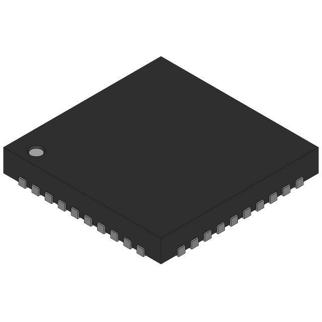


 工商网监
湘ICP备2023018690号
工商网监
湘ICP备2023018690号
