www.ti.com
Table of Contents
User’s Guide
TRF37x73 and TRF37x75 EVM
Chris Pearson
ABSTRACT
This document outlines the basic steps and functions that are required to ensure the proper operation and
quick setup of the TRF37x73 and TRF37x75 EVM. This document also includes a schematic diagram, a bill of
materials (BOM), printed-circuit board (PCB) layouts, board loss plots, and test block diagrams. Throughout this
document, the abbreviations EVM, TRF37x73/75 EVM, and the term evaluation module are synonymous with
the TRF37x73 and TRF37x75 EVM, unless otherwise noted.
Table of Contents
1 Contents.................................................................................................................................................................................. 2
2 EVM Overview......................................................................................................................................................................... 2
2.1 Schematic and BOM.......................................................................................................................................................... 2
2.2 TRF37x73/75 EVM Bill of Material..................................................................................................................................... 3
2.3 General Usage Information................................................................................................................................................ 4
3 EVM Layout............................................................................................................................................................................. 5
3.1 Description: Stack up and Material.................................................................................................................................... 5
3.2 PCB Layers........................................................................................................................................................................ 5
4 EVM Board Loss..................................................................................................................................................................... 7
5 Test Block Diagrams...............................................................................................................................................................8
5.1 Noise Figure.......................................................................................................................................................................8
5.2 Gain and P1dB...................................................................................................................................................................8
5.3 OIP3................................................................................................................................................................................... 9
6 Revision History......................................................................................................................................................................9
List of Figures
Figure 2-1. TRF37x73/75 EVM Schematic.................................................................................................................................. 2
Figure 3-1. Top Layer...................................................................................................................................................................5
Figure 3-2. Layers 2 and 3...........................................................................................................................................................5
Figure 3-3. Bottom Layer (Through Top Side)............................................................................................................................. 6
Figure 4-1. S11, S22 (Open), U1 Uninstalled.............................................................................................................................. 7
Figure 4-2. S11, S22 (Open), U1 and L1 Uninstalled, Copper Tape Replaced C1 and C2......................................................... 7
List of Tables
Table 2-1. TRF37x73/75 EVM BOM............................................................................................................................................ 3
SLAU546A – MARCH 2014 – REVISED OCTOBER 2021
Submit Document Feedback
Copyright © 2021 Texas Instruments Incorporated
TRF37x73 and TRF37x75 EVM
1
�Contents
www.ti.com
1 Contents
The TRF37x73/75 EVM consists of the following components:
•
TRF37x73/75 EVM board
2 EVM Overview
This section includes the schematic diagram, a bill of materials (BOM), and general usage information.
2.1 Schematic and BOM
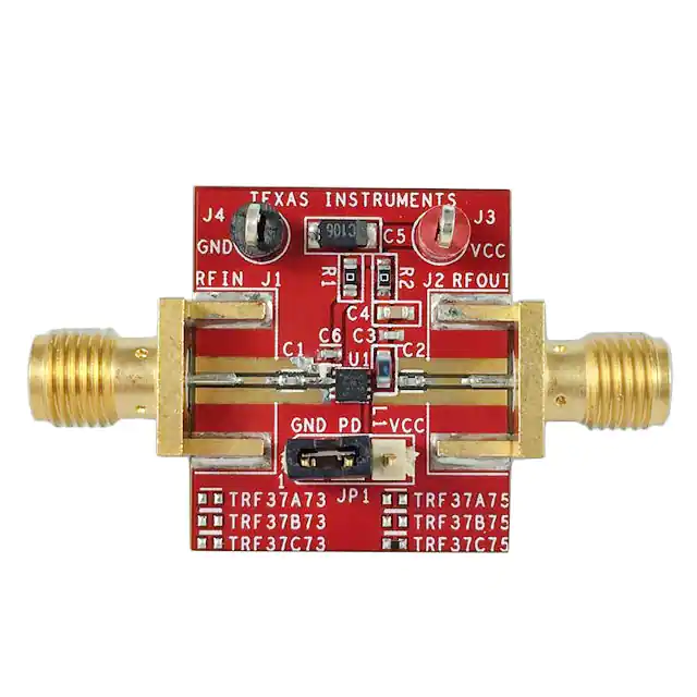
The TRF37x73/75 EVM for RF gain blocks comes in a 2 × 2 WSON package. The device type is visually
identified in component U1 by the 0402 selection resistors TRF37A73, TRF37B73, TRF37C73, TRF37A75,
TRF37B75, and TRF37C75.
The TRF37x73 are a family of 3.3-V, RF gain blocks that have 3 gain variants (A73 = 12 dB, B73 = 15 dB, and
C73 = 18 dB). The TRF37x75 are a family of 5-V, RF gain blocks that have 3 gain variants (A75 = 12 dB, B75 =
15 dB, and C75 = 18 dB).
The TRF37x73/75 EVM schematic is shown in Figure 2-1.
J4: GND
J3: VCC
C5
10 µF
R2 see BOM
R1 0Ω
C6
DNI
C3
10 pF
C4
0.01 µF
L1
100 nH
J1
RFIN
C1
1000 pF
1
8
2
7
3
6
4
5
J2
RFOUT
C2
1000 pF
U1: TRF37x7x
TRF37A73
TRF37A75
TRF37B73
TRF37B75
TRF37C73
TRF37C75
JP1: PWDN
Default Shunt 1-2
1
GND
2
3
VCC
Figure 2-1. TRF37x73/75 EVM Schematic
2
TRF37x73 and TRF37x75 EVM
SLAU546A – MARCH 2014 – REVISED OCTOBER 2021
Submit Document Feedback
Copyright © 2021 Texas Instruments Incorporated
�www.ti.com
EVM Overview
2.2 TRF37x73/75 EVM Bill of Material
Table 2-1. TRF37x73/75 EVM BOM
Common BOM
Component
Description (Footprint)
Value
Manufacturer
Part Number
C1, C2, C6
AC coupling capacitor (0402)
1000 pF
Murata
GRM1555C1H102JA01D
C3
Power Supply Decoupling (0402)
10 pF
Murata
GRM1555C1H100JZ01D
C4
Power Supply Decoupling (0603)
0.01 µF
Kemet
C0603C103K1RACTU
C5
Power Supply Decoupling
(Tantalum)
10 µF
Kemet
T494A106M016AS
J1, J2
AC signal SMA connector
Emerson Connectivity (Johnson)
142-0701-851
J3
Terminals for VCC (Clip)
Red
Keystone
5005
J4
Terminal for GND (Clip)
Black
Keystone
5006
JP1
Terminals for PWDN
L1
DC biasing inductor (0603)
100 nH
R1
DC Biasing resistor (0603)
0Ω
1:3 10 mil header
CoilCraft
0603HP-R10XJLW
TRF37A75-Specific BOM
R2
DC biasing resistor (0603)
1.8 Ω
U1
TRF37A75
5 V, 12 dB gain TI
Panasonic
TRF37A75
0402 BOM Identification resistor
0Ω
ERG-3GEYJ1R8V
TRF37A75
TRF37B75-Specific BOM
R2
DC biasing resistor (0603)
3.9 Ω
U1
TRF37B75
5 V, 15 dB gain TI
Panasonic
TRF37B75
0402 BOM Identification resistor
0Ω
ERG-3GEYJ3R9V
TRF37B75
TRF37C75-Specific BOM
R2
DC biasing resistor (0603)
6.8 Ω
U1
TRF37C75
5 V, 18 dB gain TI
Panasonic
TRF37C75
0402 BOM Identification resistor
0Ω
ERG-3GEYJ6R8V
TRF37C75
TRF37A73-Specific BOM
R2
DC biasing resistor (0603)
0Ω
U1
TRF37A73
3.3 V, 12 dB
gain
TRF37A73
0402 BOM Identification resistor
0Ω
R2
DC biasing resistor (0603)
0Ω
U1
TRF37B73
3.3 V, 15 dB
gain
TRF37B73
0402 BOM Identification resistor
0Ω
TI
TRF37A73
TRF37B73-Specific BOM
TI
TRF37B73
TRF37C73-Specific BOM
R2
DC biasing resistor (0603)
0Ω
U1
TRF37C73
3.3 V, 18 dB
gain
TRF37C73
0402 BOM Identification resistor
0Ω
TI
SLAU546A – MARCH 2014 – REVISED OCTOBER 2021
Submit Document Feedback
Copyright © 2021 Texas Instruments Incorporated
TRF37C73
TRF37x73 and TRF37x75 EVM
3
�EVM Overview
www.ti.com
2.3 General Usage Information
This section provides general usage information for the EVM.
1. Recommended power up sequence:
a. Connect GND to J4 (black – GND)
b. Connect Vcc to J3 (red – VCC)
c. Connect RF input signal to J1 (RFIN)
d. Connect measurement instrument to J2 (RFOUT)
e. Ensure the device is not in power-down mode by shorting JP1 terminals 1 and 2 or simply remove JP1
to take advantage of the TRF37x73/75’s internal pull-down resistor.
2. Power supply options:
a. For TRF37x73 devices, set VCC to 3.3 V
b. For TRF37x75 devices, set VCC to 5.0 V
3. PWDN option:
a. Short terminals 2 and 3 on JP1 to put the TRF37x73/75 in its power down state.
4. Tuning options:
a. Solder mask has been removed along the RF signal paths and VCC path allowing an easy method to
slide surface mount components along these traces for optimal tuning.
4
TRF37x73 and TRF37x75 EVM
SLAU546A – MARCH 2014 – REVISED OCTOBER 2021
Submit Document Feedback
Copyright © 2021 Texas Instruments Incorporated
�www.ti.com
EVM Layout
3 EVM Layout
3.1 Description: Stack up and Material
The TRF37x73/75 EVM is a 62-mil, 4-layer board whose material type is Isola® 370HR. The top layer routes the
power, ground, and signals to and from the device. The signal impedance is targeted at 49.9 Ω. The bottom 3
layers are ground layers.
3.2 PCB Layers
Figure 3-1 through Figure 3-3 illustrate the PCB layers for this EVM.
Figure 3-1. Top Layer
Figure 3-2. Layers 2 and 3
SLAU546A – MARCH 2014 – REVISED OCTOBER 2021
Submit Document Feedback
Copyright © 2021 Texas Instruments Incorporated
TRF37x73 and TRF37x75 EVM
5
�EVM Layout
www.ti.com
Figure 3-3. Bottom Layer (Through Top Side)
6
TRF37x73 and TRF37x75 EVM
SLAU546A – MARCH 2014 – REVISED OCTOBER 2021
Submit Document Feedback
Copyright © 2021 Texas Instruments Incorporated
�www.ti.com
EVM Board Loss
4 EVM Board Loss
Performance plots of the TRF37x73/75 EVM board are illustrated in Figure 4-1 and Figure 4-2, with the following
modifications to the BOM:
•
•
U1 gain block uninstalled
C1 and C2 removed, terminals shorted with strip of copper whose width equaled the trace width.
Figure 4-1 and Figure 4-2 show the S11 and S22 log magnitude responses to a –10-dBm input signal. These
measurements were taken with an Agilent E5071B vector network analyzer calibrated from 1 MHz to 6 GHz to
the end of the coaxial cables. The coaxial cables were connected directly to J1 and J2 on the EVM board. Port 1
refers to J1 in the schematic and Port 2 refers to J2 in the schematic.
0.0
±0.5
Sxx (dB)
±1.0
±1.5
±2.0
±2.5
S11 RFIN
S22 RFOUT
±3.0
0
1000
2000
3000
4000
5000
6000
Freq (MHz)
C001
Figure 4-1. S11, S22 (Open), U1 Uninstalled
0.0
±0.5
Sxx (dB)
±1.0
±1.5
±2.0
±2.5
S11 RFIN
S22 RFOUT
±3.0
0
1000
2000
3000
4000
5000
6000
Freq (MHz)
C002
Figure 4-2. S11, S22 (Open), U1 and L1 Uninstalled, Copper Tape Replaced C1 and C2
SLAU546A – MARCH 2014 – REVISED OCTOBER 2021
Submit Document Feedback
Copyright © 2021 Texas Instruments Incorporated
TRF37x73 and TRF37x75 EVM
7
�Test Block Diagrams
www.ti.com
5 Test Block Diagrams
This section includes recommendations, comments, and test block diagrams for noise figure, gain and P1dB,
and OIP3.
5.1 Noise Figure
Recommendations and comments:
1. Use the traditional Y-factor method
2. Take into account losses of coax to the EVM board
3. Take into account losses of traces on the board up to the input pin of the device under test (DUT)
TRF37x73/75
EVM
Spectrum or
Noise Figure
Analyzer
ENR
DIODE
5.2 Gain and P1dB
Recommendations and comments:
1. Take into account losses of coax and attenuators to and from the EVM board
2. Take into account losses of traces on the board up to the I/O pins of the DUT
3. Power meters are typically a few tenths of dB more accurate than a signal generator's level controls and
spectrum analyzer measurement capability. For precise measurements, use a power meter to measure the
output of the signal generator and output of the TRF37x73/75 EVM.
TRF37x73/75
EVM
Signal
Generator
Spectrum
Analyzer
3dB Attn
(Optional)
8
TRF37x73 and TRF37x75 EVM
3dB Attn
(Optional)
SLAU546A – MARCH 2014 – REVISED OCTOBER 2021
Submit Document Feedback
Copyright © 2021 Texas Instruments Incorporated
�www.ti.com
Test Block Diagrams
5.3 OIP3
Recommendations and comments:
1. This setup can also be used for gain and P1dB, if desired
2. For wideband measurements, the 30-dB gain stage and 10-dB attenuators are used to improve the input
IP3 level that is created from the interaction of the 2 signal generators via the isolation of the combiner.
For narrow band measurements, it maybe possible to create a setup with enough isolation using an isolator
and/or combiner. In this case the 10-dB pads could be reduced or removed.
3. Power meter A is used to ensure the amplitude of the two tones at the input of the TRF37x73/75 EVM are
within a certain tolerance. The gain stages will have unique gain characteristics and their gain can drift over
time
4. Power meter B can be used for measuring the amplitude of individual tones for more accurate
measurements.
5. Keep spectrum analyzer RBW and VBW settings identical for main tone and IM3 products
6. Take into account losses of coax and attenuators to and from the EVM board
7. Take into account losses of traces on the board up to the I/O pins of the DUT
Power Meter
Input B
Power Meter
Input A
Signal
Generator
A
30dB Gain
10dB Attn
3dB Attn
Combiner
Signal
Generator
B
3dB Attn
3dB Attn
30dB Gain
TRF37x73/75
EVM
3dB Attn
Coupler
Splitter or
Coupler
3dB Attn
Spectrum
Analyzer
10dB Attn
6 Revision History
NOTE: Page numbers for previous revisions may differ from page numbers in the current version.
Changes from Revision * (March 2014) to Revision A (October 2021)
Page
• Updated the numbering format for tables, figures, and cross-references throughout the document..................2
• Updated the L1 components part number from -6-3HP-F10XJLU to 0603HP-R10XJLW in the TRF37x73/75
EVM BOM table.................................................................................................................................................. 3
SLAU546A – MARCH 2014 – REVISED OCTOBER 2021
Submit Document Feedback
Copyright © 2021 Texas Instruments Incorporated
TRF37x73 and TRF37x75 EVM
9
�IMPORTANT NOTICE AND DISCLAIMER
TI PROVIDES TECHNICAL AND RELIABILITY DATA (INCLUDING DATA SHEETS), DESIGN RESOURCES (INCLUDING REFERENCE
DESIGNS), APPLICATION OR OTHER DESIGN ADVICE, WEB TOOLS, SAFETY INFORMATION, AND OTHER RESOURCES “AS IS”
AND WITH ALL FAULTS, AND DISCLAIMS ALL WARRANTIES, EXPRESS AND IMPLIED, INCLUDING WITHOUT LIMITATION ANY
IMPLIED WARRANTIES OF MERCHANTABILITY, FITNESS FOR A PARTICULAR PURPOSE OR NON-INFRINGEMENT OF THIRD
PARTY INTELLECTUAL PROPERTY RIGHTS.
These resources are intended for skilled developers designing with TI products. You are solely responsible for (1) selecting the appropriate
TI products for your application, (2) designing, validating and testing your application, and (3) ensuring your application meets applicable
standards, and any other safety, security, regulatory or other requirements.
These resources are subject to change without notice. TI grants you permission to use these resources only for development of an
application that uses the TI products described in the resource. Other reproduction and display of these resources is prohibited. No license
is granted to any other TI intellectual property right or to any third party intellectual property right. TI disclaims responsibility for, and you
will fully indemnify TI and its representatives against, any claims, damages, costs, losses, and liabilities arising out of your use of these
resources.
TI’s products are provided subject to TI’s Terms of Sale or other applicable terms available either on ti.com or provided in conjunction with
such TI products. TI’s provision of these resources does not expand or otherwise alter TI’s applicable warranties or warranty disclaimers for
TI products.
TI objects to and rejects any additional or different terms you may have proposed. IMPORTANT NOTICE
Mailing Address: Texas Instruments, Post Office Box 655303, Dallas, Texas 75265
Copyright © 2022, Texas Instruments Incorporated
�