www.ti.com
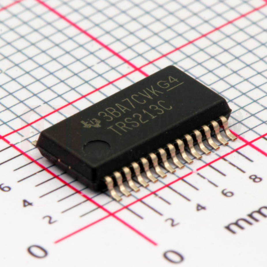
TRS213
5-V MULTICHANNEL RS-232 LINE DRIVER/RECEIVER
WITH ±15-kV ESD PROTECTION
FEATURES
•
•
•
•
•
•
•
•
•
ESD Protection for RS-232 Bus Pins
– ±15-kV Human-Body Model (HBM)
Meets or Exceeds the Requirements of
TIA/EIA-232-F and ITU v.28 Standards
Operates at 5-V VCC Supply
Four Drivers and Five Receivers
Operates up to 120 kbit/s
Low Supply Current in Shutdown
Mode . . . 15 μA Typ
External Capacitors . . . 4 × 0.1 F
Designed to Be Interchangeable With Industry
Standard '213 Devices
Latch-Up Performance Exceeds 100 mA Per
JESD 78, Class II
SLLS807 – JUNE 2007
DB, DW, OR PW PACKAGE
(TOP VIEW)
DOUT3
DOUT1
DOUT2
RIN2
ROUT2
DIN2
DIN1
ROUT1
RIN1
GND
VCC
C1+
V+
C1–
1
28
2
27
3
26
4
25
5
24
6
23
7
22
8
9
21
10
19
11
18
12
17
13
16
14
15
20
DOUT4
RIN3
ROUT3
SHDN
EN
RIN4
ROUT4
DIN4
DIN3
ROUT5
RIN5
V–
C2–
C2+
APPLICATIONS
•
•
•
•
•
•
Battery-Powered Systems
PDAs
Notebooks
Laptops
Palmtop PCs
Hand-Held Equipment
DESCRIPTION/ ORDER INFORMATION
The TRS213 device consists of four line drivers, five line receivers, and a dual charge-pump circuit with ±15-kV
ESD protection pin to pin (serial-port connection pins, including GND). The device meets the requirements of
TIA/EIA-232-F and provides the electrical interface between an asynchronous communication controller and the
serial-port connector. The charge pump and four small external capacitors allow operation from a single 5-V
supply. The devices operate at data signaling rates up to 120 kbit/s and a maximum of 30-V/μs driver output
slew rate.
The TRS213 has an active-low shutdown (SHDN) and an active-high enable control (EN). In shutdown mode,
the charge pumps are turned off, V+ is pulled down to VCC, V– is pulled to GND, and the transmitter outputs are
disabled. This reduces supply current typically to 1 μA. Two receivers of the TRS213 are active during
shutdown.
Please be aware that an important notice concerning availability, standard warranty, and use in critical applications of Texas
Instruments semiconductor products and disclaimers thereto appears at the end of this data sheet.
PRODUCTION DATA information is current as of publication date.
Products conform to specifications per the terms of the Texas
Instruments standard warranty. Production processing does not
necessarily include testing of all parameters.
Copyright © 2007, Texas Instruments Incorporated
�TRS213
5-V MULTICHANNEL RS-232 LINE DRIVER/RECEIVER
WITH ±15-kV ESD PROTECTION
www.ti.com
SLLS807 – JUNE 2007
ORDERING INFORMATION
TA
PACKAGE
SOIC – DW
0°C to 70°C
SSOP – DB
TSSOP – PW
SOIC – DW
–40°C to 85°C
SSOP – DB
TSSOP – PW
(1)
(2)
(1) (2)
ORDERABLE PART NUMBER
Tube of 20
TRS213CDW
Reel of 1000
TRS213CDWR
Tube of 50
TRS213CDB
Reel of 2000
TRS213CDBR
Tape and reel
TRS213CPWR
Tube of 20
TRS213IDW
Reel of 1000
TRS213IDWR
Tube of 50
TRS213IDB
Reel of 2000
TRS213IDBR
Tape and reel
TRS213IPWR
TOP-SIDE MARKING
TRS213C
TRS213C
TRS213C
TRS213I
TRS213I
TRS213I
Package drawings, standard packing quantities, thermal data, symbolization, and PCB design guidelines are available at
www.ti.com/sc/package.
For the most current package and ordering information, see the Package Option Addendum at the end of this document, or see the TI
website at www.ti.com.
FUNCTION TABLE
INPUTS
(1)
2
RECEIVER
EN
DRIVER
D1–D4
R1–R3
L
L
Z
Z
Z
Shutdown
L
H
Z
Z
Active (1)
Shutdown
H
L
All active
Z
Z
Normal operation
H
H
All active
Active
Active
Normal operation
SHDN
R4–R5
See the VIT+ and VIT– change in the Electrical Characteristics table.
Submit Documentation Feedback
DEVICE STATUS
�TRS213
5-V MULTICHANNEL RS-232 LINE DRIVER/RECEIVER
WITH ±15-kV ESD PROTECTION
www.ti.com
SLLS807 – JUNE 2007
LOGIC DIAGRAM (POSITIVE LOGIC)
7
2
DIN1
DOUT1
6
3
DIN2
TTL/CMOS
Inputs
DOUT2
20
RS-232
Outputs
1
DIN3
DOUT3
21
28
DIN4
DOUT4
25
24
SHDN
EN
89
ROUT1
RIN1
5
4
ROUT2
TTL/CMOS
Outputs
RIN2
26
27
ROUT3
RIN3
22
RS-232
Inputs
23
ROUT4
RIN4
19
18
ROUT5
RIN5
Submit Documentation Feedback
3
�TRS213
5-V MULTICHANNEL RS-232 LINE DRIVER/RECEIVER
WITH ±15-kV ESD PROTECTION
www.ti.com
SLLS807 – JUNE 2007
Absolute Maximum Ratings (1)
over operating free-air temperature range (unless otherwise noted)
VCC
Supply voltage range
V+
Positive charge-pump voltage range (2)
V–
Negative charge-pump voltage range
VI
Input voltage range
VO
Output voltage range
DOUT
Short-circuit duration
θJA
Package thermal impedance (3) (4)
(2)
Drivers
MIN
MAX
–0.3
6
V
VCC – 0.3
14
V
0.3
–14
V
–0.3
V+ + 0.3
±30
Receivers
Drivers
Receivers
V– – 0.3
V+ + 0.3
–0.3
VCC + 0.3
UNIT
V
V
Continuous
DB package
62
DW package
46
C°/W
150
C°
150
C°
PW package
TJ
Operating virtual junction temperature
Tstg
Storage temperature range
(1)
(2)
(3)
(4)
–65
Stresses beyond those listed under "absolute maximum ratings" may cause permanent damage to the device. These are stress ratings
only, and functional operation of the device at these or any other conditions beyond those indicated under "recommended operating
conditions" is not implied. Exposure to absolute-maximum-rated conditions for extended periods may affect device reliability.
All voltages are with respect to network GND.
Maximum power dissipation is a function of TJ(max),θJA, and TA. The maximum allowable power dissipation at any allowable ambient
temperature is PD = (TJ(max) – TA)/θJA. Operating at the absolute maximum TJ of 150°C can affect reliability.
The package thermal impedance is calculated in accordance with JESD 51-7.
Recommended Operating Conditions (1)
See Figure 4
Supply voltage
VIH
VIL
VI
TA
(1)
Driver high-level input voltage
DIN
Control high-level input voltage
EN, SHDN
Driver and control low-level input voltage
DIN, EN, SHDN
Driver and control input voltage
DIN, EN, SHDN
Receiver input voltage
RIN
MIN
NOM
MAX
4.5
5
5.5
2
TRS213I
V
V
2.4
0.8
0
5.5
–30
30
0
70
–40
85
TRS213C
Operating free-air temperature
UNIT
V
V
°C
Test conditions are C1–C4 = 0.1 μF at VCC = 5 V ± 0.5 V.
Electrical Characteristics (1)
over operating free-air temperature range (unless otherwise noted)
PARAMETER
MIN
TYP (2)
MAX
UNIT
ICC
Supply current
No load,
See Figure 6
14
20
mA
ISHDN
Shutdown supply current
TA = 25°C,
See Figure 1
15
50
μA
(1)
(2)
4
TEST CONDITIONS
Test conditions are C1–C4 = 0.1 μF at VCC = 5 V ± 0.5 V.
All typical values are at VCC = 5 V, and TA = 25°C.
Submit Documentation Feedback
�TRS213
5-V MULTICHANNEL RS-232 LINE DRIVER/RECEIVER
WITH ±15-kV ESD PROTECTION
www.ti.com
SLLS807 – JUNE 2007
DRIVER SECTION
Electrical Characteristics (1)
over operating free-air temperature range (unless otherwise noted) (see Figure 4)
PARAMETER
TEST CONDITIONS
MIN
TYP (2)
VOH
High-level output voltage
DOUT at RL = 3 kΩ to GND
5
9
VOL
Low-level output voltage
DOUT at RL = 3 kΩ to GND
–5
–9
IIH
Control high-level input current
EN, SHDN = 5 V
Driver low-level input current
DIN = 0 V
Control low-level input current
EN, SHDN = 0 V
IOS (3)
Short-circuit output current
VCC = 5.5 V,
VO = 0 V
ro
Output resistance
VCC, V+, and V– = 0 V,
VO = ±2 V
IIL
(1)
(2)
(3)
MAX
UNIT
V
V
3
10
–15
–200
–3
–10
±10
±60
μA
μA
mA
Ω
300
Test conditions are C1–C4 = 0.1 μF at VCC = 5 V ± 0.5 V
All typical values are at VCC = 5 V, and TA = 25°C.
Short-circuit durations should be controlled to prevent exceeding the device absolute power dissipation ratings, and not more than one
output should be shorted at a time.
Switching Characteristics (1)
over operating free-air temperature range (unless otherwise noted)
PARAMETER
TEST CONDITIONS
MIN TYP (2)
MAX
UNIT
Maximum data rate
CL = 50 pF to 1000 pF,
One DOUT switching,
RL = 3 kΩ to 7 kΩ,
See Figure 3
tPLH(D)
Propagation delay time,
low- to high-level output
CL = 2500 pF,
All drivers loaded,
RL = 3 kΩ,
See Figure 3
2
μs
tPHL(D)
Propagation delay time,
high- to low-level output
CL = 2500 pF,
All drivers loaded,
RL = 3 kΩ,
See Figure 3
2
μs
tsk(p)
Pulse skew (3)
CL = 150 pF to 2500 pF,
See Figure 3
RL = 3 kΩ to 7 kΩ,
300
ns
SR(tr)
Slew rate, transition region
(see Figure 2)
CL = 50 pF to 1000 pF,
VCC = 5 V
RL = 3 kΩ to 7 kΩ,
(1)
(2)
(3)
120
3
kbit/s
6
30
V/μs
Test conditions are C1–C4 = 0.1 μF at VCC = 5 V ± 0.5 V.
All typical values are at VCC = 5 V, and TA = 25°C.
Pulse skew is defined as (tPLH – tPHL) of each channel of the same device.
ESD Protection
over operating free-air temperature range (unless otherwise noted)
PIN
DOUT
TEST CONDITIONS
Human-Body Model
Submit Documentation Feedback
TYP
UNIT
±15
kV
5
�TRS213
5-V MULTICHANNEL RS-232 LINE DRIVER/RECEIVER
WITH ±15-kV ESD PROTECTION
www.ti.com
SLLS807 – JUNE 2007
RECEIVER SECTION
Electrical Characteristics (1)
over operating free-air temperature range (unless otherwise noted) (see Figure 6)
PARAMETER
TEST CONDITIONS
VOH
High-level output voltage
IOH = –1 mA
VOL
Low-level output voltage
IOH = 1.6 mA
TYP (2)
MAX
VCC – 0.4
Active mode
1.7
2.4
Shutdown mode (R4–R5)
1.5
2.4
Positive-going
input threshold voltage
VCC = 5 V, TA = 25°C
VIT–
Negative-going
input threshold voltage
VCC = 5 V, TA = 25°C
Vhys (3)
Input hysteresis (VIT+, VIT–)
VCC = 5 V
rI
Input resistance
VCC = 5 V, TA = 25°C
Output leakage current
EN = 0 V, 0 ≤ ROUT ≤ VCC, R1–R3
Active mode
0.8
1.2
Shutdown mode (R4–R5)
0.6
1.5
3
UNIT
V
0.4
VIT+
(1)
(2)
(3)
MIN
V
V
V
0.5
1
V
5
7
kΩ
±0.05
±10
μA
MIN TYP (2)
MAX
UNIT
0.5
10
4
40
10
Test conditions are C1–C4 = 0.1 μF at VCC = 5 V ± 0.5 V.
All typical values are at VCC = 5 V, and TA = 25°C.
No hysteresis in shudown mode
Switching Characteristics (1)
over operating free-air temperature range (unless otherwise noted)
PARAMETER
TEST CONDITIONS
SHDN = VCC
tPLH(R)
Propagation delay time,
low- to high-level output
CL = 150 pF,
See Figure 4
tPHL(R)
Propagation delay time,
high- to low-level output
CL = 150 pF,
See Figure 4
0.5
ten
Output enable time
CL = 150 pF,
See Figure 5
600
ns
tdis
Output disable time
CL = 150 pF,
See Figure 5
200
ns
(1)
(2)
SHDN = 0 V, R4–R5
μs
μs
Test conditions are C1–C4 = 0.1 μF at VCC = 5 V ± 0.5 V.
All typical values are at VCC = 5 V, and TA = 25°C.
ESD Protection
over operating free-air temperature range (unless otherwise noted)
PIN
RIN
6
TEST CONDITIONS
Human-Body Model
Submit Documentation Feedback
TYP
UNIT
±15
kV
�TRS213
5-V MULTICHANNEL RS-232 LINE DRIVER/RECEIVER
WITH ±15-kV ESD PROTECTION
www.ti.com
SLLS807 – JUNE 2007
PARAMETER MEASUREMENT INFORMATION
0.1 mF
+
–
ISHDN
5.5 V
0.1 mF
+
–
VCC
V+
C1+
0.1 mF
+
–
V–
0.1 mF
– +
C1–
C2+
0.1 mF
+
–
C2–
VCC
400 kΩ
5.5 V
DOUT
DIN
D1−D4
RIN
ROUT
0-V or 5.5-V Drive
5.5 V
3 kΩ
5.5 V
EN
5 kΩ
R1−R5
SHDN
GND
Figure 1. Shutdown Current Test Circuit
Submit Documentation Feedback
7
�TRS213
5-V MULTICHANNEL RS-232 LINE DRIVER/RECEIVER
WITH ±15-kV ESD PROTECTION
www.ti.com
SLLS807 – JUNE 2007
5-V
SHDN
Input
Generator
(see Note B)
RS-232
Output
3V
1.5 V
1.5 V
0V
50 Ω
RL
tTHL(D)
CL
(see Note A)
Output
tTLH(D)
3V
–3 V
TEST CIRCUIT
SR(tr) =
6V
tTHL(D) or tTLH(D)
VOH
3V
–3 V
VOL
VOLTAGE WAVEFORMS
NOTES: A. CL includes probe and jig capacitance.
B. The pulse generator has the following characteristics: ZO = 50 Ω, 50% duty cycle, tr ≤ 10 ns, tf ≤ 10 ns.
Figure 2. Driver Slew Rate
5-V
SHDN
3V
Generator
(see Note B)
RS-232
Output
Input
1.5 V
0V
50 Ω
RL
1.5 V
tPHL(D)
CL
(see Note A)
tPLH(D)
VOH
50%
50%
Output
VOL
TEST CIRCUIT
VOLTAGE WAVEFORMS
NOTES: A. CL includes probe and jig capacitance.
B. The pulse generator has the following characteristics: ZO = 50 Ω, 50% duty cycle, tr ≤ 10 ns, tf ≤ 10 ns.
Figure 3. Driver Pulse Skew and Propagation Delay Times
5-V
SHDN
3V
Input
1.5 V
1.5 V
–3 V
Output
Generator
(see Note B)
50 Ω
tPHL(R)
tPLH(R)
CL
(see Note A)
5-V
EN
VOH
50%
Output
50%
VOL
TEST CIRCUIT
VOLTAGE WAVEFORMS
NOTES: A. CL includes probe and jig capacitance.
B. The pulse generator has the following characteristics: ZO = 50 Ω, 50% duty cycle, tr ≤ 10 ns, tf ≤ 10 ns.
Figure 4. Receiver Propagation Delay Times
8
Submit Documentation Feedback
�TRS213
5-V MULTICHANNEL RS-232 LINE DRIVER/RECEIVER
WITH ±15-kV ESD PROTECTION
www.ti.com
SLLS807 – JUNE 2007
3V
5-V
SHDN
VCC
S1
GND
1.5 V
0V
tPZH
(S1 at GND)
tPHZ
(S1 at GND)
RL
3 V or 0 V
1.5 V
Input
Output
Output
VOH
3.5 V
VOH – 0.1 V
CL
(see Note A)
EN
Generator
(see Note B)
50 Ω
tPZL
(S1 at VCC)
tPLZ
(S1 at VCC)
VOL + 0.1 V
0.8 V
Output
TEST CIRCUIT
NOTES: A.
B.
C.
D.
VOL
VOLTAGE WAVEFORMS
CL includes probe and jig capacitance.
The pulse generator has the following characteristics: ZO = 50 Ω, 50% duty cycle, tr ≤ 10 ns, tf ≤ 10 ns.
tPLZ and tPHZ are the same as tdis.
tPZL and tPZH are the same as ten.
Figure 5. Receiver Enable and Disable Times
Submit Documentation Feedback
9
�TRS213
5-V MULTICHANNEL RS-232 LINE DRIVER/RECEIVER
WITH ±15-kV ESD PROTECTION
www.ti.com
SLLS807 – JUNE 2007
APPLICATION INFORMATION
DOUT3
DOUT1
DOUT2
RIN2
1
28
2
27
3
RIN3
5 kΩ
4
26
5 kΩ
ROUT2
DOUT4
25
ROUT3
SHDN = 5 V
24
5
EN
23
5V
RIN4
5 kΩ
400 kΩ
DIN2
6
22
ROUT4
5V
400 kΩ
DIN1
ROUT1
RIN1
GND
5V
7
400 kΩ
21
8
9
DIN4
5V
10
5 kΩ
400 kΩ
20
–
DIN3
CBYPASS
= 0.1 mF
+
11
VCC
C3(1) =
–
0.1 mF
6.3 V
+
18
12
13
C1 =
0.1 mF
6.3 V
19
VCC
C1+
C4 =
0.1 mF
16 V
5 kΩ
V–
14
RIN5
V+
+
–
ROUT5
C1–
C2–
17
–
16
–
+
C2+
+
C2 =
0.1 mF
16 V
15
(1) C3 can be connected to VCC or GND.
NOTES: A. Resistor values shown are nominal.
B. Nonpolarized ceramic capacitors are acceptable. If polarized tantalum or electrolytic capacitors are used, they
should be connected as shown.
Figure 6. Typical Operating Circuit and Capacitor Values
10
Submit Documentation Feedback
�PACKAGE OPTION ADDENDUM
www.ti.com
17-Mar-2017
PACKAGING INFORMATION
Orderable Device
Status
(1)
Package Type Package Pins Package
Drawing
Qty
Eco Plan
Lead/Ball Finish
MSL Peak Temp
(2)
(6)
(3)
Op Temp (°C)
Device Marking
(4/5)
TRS213CDBR
ACTIVE
SSOP
DB
28
2000
Green (RoHS
& no Sb/Br)
CU NIPDAU
Level-1-260C-UNLIM
0 to 70
TRS213C
TRS213IDB
ACTIVE
SSOP
DB
28
50
Green (RoHS
& no Sb/Br)
CU NIPDAU
Level-1-260C-UNLIM
-40 to 85
TRS213I
TRS213IDBR
ACTIVE
SSOP
DB
28
2000
Green (RoHS
& no Sb/Br)
CU NIPDAU
Level-1-260C-UNLIM
-40 to 85
TRS213I
TRS213IDWR
ACTIVE
SOIC
DW
28
1000
Green (RoHS
& no Sb/Br)
CU NIPDAU
Level-1-260C-UNLIM
-40 to 85
TRS213I
(1)
The marketing status values are defined as follows:
ACTIVE: Product device recommended for new designs.
LIFEBUY: TI has announced that the device will be discontinued, and a lifetime-buy period is in effect.
NRND: Not recommended for new designs. Device is in production to support existing customers, but TI does not recommend using this part in a new design.
PREVIEW: Device has been announced but is not in production. Samples may or may not be available.
OBSOLETE: TI has discontinued the production of the device.
(2)
Eco Plan - The planned eco-friendly classification: Pb-Free (RoHS), Pb-Free (RoHS Exempt), or Green (RoHS & no Sb/Br) - please check http://www.ti.com/productcontent for the latest availability
information and additional product content details.
TBD: The Pb-Free/Green conversion plan has not been defined.
Pb-Free (RoHS): TI's terms "Lead-Free" or "Pb-Free" mean semiconductor products that are compatible with the current RoHS requirements for all 6 substances, including the requirement that
lead not exceed 0.1% by weight in homogeneous materials. Where designed to be soldered at high temperatures, TI Pb-Free products are suitable for use in specified lead-free processes.
Pb-Free (RoHS Exempt): This component has a RoHS exemption for either 1) lead-based flip-chip solder bumps used between the die and package, or 2) lead-based die adhesive used between
the die and leadframe. The component is otherwise considered Pb-Free (RoHS compatible) as defined above.
Green (RoHS & no Sb/Br): TI defines "Green" to mean Pb-Free (RoHS compatible), and free of Bromine (Br) and Antimony (Sb) based flame retardants (Br or Sb do not exceed 0.1% by weight
in homogeneous material)
(3)
MSL, Peak Temp. - The Moisture Sensitivity Level rating according to the JEDEC industry standard classifications, and peak solder temperature.
(4)
There may be additional marking, which relates to the logo, the lot trace code information, or the environmental category on the device.
(5)
Multiple Device Markings will be inside parentheses. Only one Device Marking contained in parentheses and separated by a "~" will appear on a device. If a line is indented then it is a continuation
of the previous line and the two combined represent the entire Device Marking for that device.
(6)
Lead/Ball Finish - Orderable Devices may have multiple material finish options. Finish options are separated by a vertical ruled line. Lead/Ball Finish values may wrap to two lines if the finish
value exceeds the maximum column width.
Addendum-Page 1
Samples
�PACKAGE OPTION ADDENDUM
www.ti.com
17-Mar-2017
Important Information and Disclaimer:The information provided on this page represents TI's knowledge and belief as of the date that it is provided. TI bases its knowledge and belief on information
provided by third parties, and makes no representation or warranty as to the accuracy of such information. Efforts are underway to better integrate information from third parties. TI has taken and
continues to take reasonable steps to provide representative and accurate information but may not have conducted destructive testing or chemical analysis on incoming materials and chemicals.
TI and TI suppliers consider certain information to be proprietary, and thus CAS numbers and other limited information may not be available for release.
In no event shall TI's liability arising out of such information exceed the total purchase price of the TI part(s) at issue in this document sold by TI to Customer on an annual basis.
Addendum-Page 2
�PACKAGE MATERIALS INFORMATION
www.ti.com
12-Feb-2019
TAPE AND REEL INFORMATION
*All dimensions are nominal
Device
Package Package Pins
Type Drawing
TRS213CDBR
SSOP
TRS213IDBR
TRS213IDWR
SPQ
Reel
Reel
A0
Diameter Width (mm)
(mm) W1 (mm)
K0
(mm)
P1
(mm)
W
Pin1
(mm) Quadrant
10.5
2.5
12.0
16.0
Q1
DB
28
2000
330.0
16.4
SSOP
DB
28
2000
330.0
16.4
8.2
10.5
2.5
12.0
16.0
Q1
SOIC
DW
28
1000
330.0
32.4
11.35
18.67
3.1
16.0
32.0
Q1
Pack Materials-Page 1
8.2
B0
(mm)
�PACKAGE MATERIALS INFORMATION
www.ti.com
12-Feb-2019
*All dimensions are nominal
Device
Package Type
Package Drawing
Pins
SPQ
Length (mm)
Width (mm)
Height (mm)
TRS213CDBR
SSOP
DB
28
2000
367.0
367.0
38.0
TRS213IDBR
SSOP
DB
28
2000
367.0
367.0
38.0
TRS213IDWR
SOIC
DW
28
1000
350.0
350.0
66.0
Pack Materials-Page 2
��PACKAGE OUTLINE
DB0028A
SSOP - 2 mm max height
SCALE 1.500
SMALL OUTLINE PACKAGE
C
8.2
TYP
7.4
A
0.1 C
PIN 1 INDEX AREA
SEATING
PLANE
26X 0.65
28
1
2X
10.5
9.9
NOTE 3
8.45
14
15
28X
B
5.6
5.0
NOTE 4
SEE DETAIL A
(0.15) TYP
0.38
0.22
0.15
C A B
2 MAX
0.25
GAGE PLANE
0 -8
0.95
0.55
0.05 MIN
DETAIL A
A 15
TYPICAL
4214853/B 03/2018
NOTES:
1. All linear dimensions are in millimeters. Any dimensions in parenthesis are for reference only. Dimensioning and tolerancing
per ASME Y14.5M.
2. This drawing is subject to change without notice.
3. This dimension does not include mold flash, protrusions, or gate burrs. Mold flash, protrusions, or gate burrs shall not
exceed 0.15 mm per side.
4. This dimension does not include interlead flash. Interlead flash shall not exceed 0.25 mm per side.
5. Reference JEDEC registration MO-150.
www.ti.com
�EXAMPLE BOARD LAYOUT
DB0028A
SSOP - 2 mm max height
SMALL OUTLINE PACKAGE
SYMM
28X (1.85)
(R0.05) TYP
1
28X (0.45)
28
26X (0.65)
SYMM
15
14
(7)
LAND PATTERN EXAMPLE
EXPOSED METAL SHOWN
SCALE: 10X
SOLDER MASK
OPENING
SOLDER MASK
OPENING
METAL UNDER
SOLDER MASK
METAL
EXPOSED METAL
EXPOSED METAL
0.07 MAX
ALL AROUND
NON-SOLDER MASK
DEFINED
(PREFERRED)
0.07 MIN
ALL AROUND
SOLDER MASK
DEFINED
SOLDER MASK DETAILS
15.000
4214853/B 03/2018
NOTES: (continued)
6. Publication IPC-7351 may have alternate designs.
7. Solder mask tolerances between and around signal pads can vary based on board fabrication site.
www.ti.com
�EXAMPLE STENCIL DESIGN
DB0028A
SSOP - 2 mm max height
SMALL OUTLINE PACKAGE
28X (1.85)
SYMM
(R0.05) TYP
1
28X (0.45)
28
26X (0.65)
SYMM
14
15
(7)
SOLDER PASTE EXAMPLE
BASED ON 0.125 mm THICK STENCIL
SCALE: 10X
4214853/B 03/2018
NOTES: (continued)
8. Laser cutting apertures with trapezoidal walls and rounded corners may offer better paste release. IPC-7525 may have alternate
design recommendations.
9. Board assembly site may have different recommendations for stencil design.
www.ti.com
�IMPORTANT NOTICE AND DISCLAIMER
TI PROVIDES TECHNICAL AND RELIABILITY DATA (INCLUDING DATASHEETS), DESIGN RESOURCES (INCLUDING REFERENCE
DESIGNS), APPLICATION OR OTHER DESIGN ADVICE, WEB TOOLS, SAFETY INFORMATION, AND OTHER RESOURCES “AS IS”
AND WITH ALL FAULTS, AND DISCLAIMS ALL WARRANTIES, EXPRESS AND IMPLIED, INCLUDING WITHOUT LIMITATION ANY
IMPLIED WARRANTIES OF MERCHANTABILITY, FITNESS FOR A PARTICULAR PURPOSE OR NON-INFRINGEMENT OF THIRD
PARTY INTELLECTUAL PROPERTY RIGHTS.
These resources are intended for skilled developers designing with TI products. You are solely responsible for (1) selecting the appropriate
TI products for your application, (2) designing, validating and testing your application, and (3) ensuring your application meets applicable
standards, and any other safety, security, or other requirements. These resources are subject to change without notice. TI grants you
permission to use these resources only for development of an application that uses the TI products described in the resource. Other
reproduction and display of these resources is prohibited. No license is granted to any other TI intellectual property right or to any third
party intellectual property right. TI disclaims responsibility for, and you will fully indemnify TI and its representatives against, any claims,
damages, costs, losses, and liabilities arising out of your use of these resources.
TI’s products are provided subject to TI’s Terms of Sale (www.ti.com/legal/termsofsale.html) or other applicable terms available either on
ti.com or provided in conjunction with such TI products. TI’s provision of these resources does not expand or otherwise alter TI’s applicable
warranties or warranty disclaimers for TI products.
Mailing Address: Texas Instruments, Post Office Box 655303, Dallas, Texas 75265
Copyright © 2019, Texas Instruments Incorporated
�


 工商网监
湘ICP备2023018690号
工商网监
湘ICP备2023018690号