Product
Folder
Order
Now
Support &
Community
Tools &
Software
Technical
Documents
TS3A5223
SCDS339B – JANUARY 2013 – REVISED APRIL 2017
TS3A5223 0.45 Ω 2-Channel SPDT Bidirectional Analog Switch
1 Features
3 Description
•
The TS3A5223 is a high-speed 2-channel analog
switch with break-before-make and bi-directional
signal switching capability. The TS3A5223 can be
used as a dual 2:1 multiplexer or a 1:2 dual demultiplexer.
1
•
•
•
•
•
•
•
•
•
•
Low ON Resistance Switches
– 0.45 Ω (Typical) at 3.6 V
– 0.85 Ω (Typical) at 1.8 V
Wide Supply Range: 1.65 V to 3.6 V
1.0 V Compatible Logic Interface
High Switch Bandwidth 80 MHz
0.01% THD Across Entire Band
Specified min Break-before-make
Bi-directional Switching
–75 dB Channel-to-Channel Crosstalk
–70 dB Channel-to-Channel OFF Isolation of Very
Low Power Dissipation and Leakage Currents
Very Small QFN-10 Package: 1.8 mm × 1.4 mm
ESD Protection on all Pins
– 2 kV HBM, 500 V CDM
The TS3A5223 offers very low ON resistance, very
low THD, channel-to-channel crosstalk and very high
OFF isolation. These features make TS3A5223
suitable for application in Audio signal routing and
switching applications.
The TS3A5223 control logic supports 1 V – 3.6 V
CMOS logic levels. The logic interface allows direct
interface with a wide range of CPUs and
microcontrollers without increasing the current drawn
from supply (ICC) and thus lowering power
consumption.
Device Information(1)
PART NUMBER
PACKAGE
BODY SIZE (NOM)
2 Applications
TS3A5223
•
•
•
•
(1) For all available packages, see the orderable addendum at
the end of the data sheet.
Portable Electronics
Smartphones, Tablets
Home Electronics
Wireline Communication
µQFN (10)
1.80 mm x 1.40 mm
Functional Diagram
NC1
COM1
NO1
SEL1
Level
Shifter
NC2
COM2
NO2
SEL2
Level
Shifter
Copyright © 2017, Texas Instruments Incorporated
1
An IMPORTANT NOTICE at the end of this data sheet addresses availability, warranty, changes, use in safety-critical applications,
intellectual property matters and other important disclaimers. PRODUCTION DATA.
�TS3A5223
SCDS339B – JANUARY 2013 – REVISED APRIL 2017
www.ti.com
Table of Contents
1
2
3
4
5
6
7
8
Features ..................................................................
Applications ...........................................................
Description .............................................................
Revision History.....................................................
Pin Configuration and Functions .........................
Specifications.........................................................
1
1
1
2
3
4
6.1
6.2
6.3
6.4
6.5
6.6
4
4
4
4
5
6
Absolute Maximum Ratings ......................................
ESD Ratings ............................................................
Recommended Operating Conditions.......................
Thermal Information ..................................................
Electrical Characteristics...........................................
Typical Characteristics ..............................................
Parameter Measurement Information .................. 7
Detailed Description ............................................ 10
8.1 Overview ................................................................. 10
8.2 Functional Block Diagram ....................................... 10
8.3 Feature Description................................................. 10
8.4 Device Functional Modes........................................ 11
9
Application and Implementation ........................ 12
9.1 Application Information............................................ 12
9.2 Typical Application ................................................. 12
10 Power Supply Recommendations ..................... 13
11 Layout................................................................... 14
11.1 Layout Guidelines ................................................. 14
11.2 Layout Example .................................................... 14
12 Device and Documentation Support ................. 15
12.1
12.2
12.3
12.4
12.5
12.6
Documentation Support .......................................
Receiving Notification of Documentation Updates
Community Resources..........................................
Trademarks ...........................................................
Electrostatic Discharge Caution ............................
Glossary ................................................................
15
15
15
15
15
15
13 Mechanical, Packaging, and Orderable
Information ........................................................... 15
4 Revision History
NOTE: Page numbers for previous revisions may differ from page numbers in the current version.
Changes from Revision A (February 2013) to Revision B
Page
•
Added the Device Information table, ESD Ratings table, Thermal Information table, Feature Description section,
Device Functional Modes, Application and Implementation section, Power Supply Recommendations section,
Layout section, Device and Documentation Support section, and Mechanical, Packaging, and Orderable Information
section .................................................................................................................................................................................... 1
•
Changed the VMax MAX value From: 3.6 V To: VCC in the Recommended Operating Conditions table ................................ 4
•
Deleted: "dt/dv, SEL pin Input rise and fall time limit" from the Recommended Operating Conditions table......................... 4
•
Deleted the Dissipation Ratings table..................................................................................................................................... 4
Changes from Original (January 2013) to Revision A
•
2
Page
Changed the device status From: Preview To: Production ................................................................................................... 1
Submit Documentation Feedback
Copyright © 2013–2017, Texas Instruments Incorporated
Product Folder Links: TS3A5223
�TS3A5223
www.ti.com
SCDS339B – JANUARY 2013 – REVISED APRIL 2017
5 Pin Configuration and Functions
RSW Package
10 Pin UQFN
Top View
10
NO2
GND
COM2
6
9
NC2
SEL2
7
8
NC1
5
SEL1
4
COM1
3
2
1
NO1
VCC
TS3A5223
Pin Functions
NAME
PIN NUMBER
VCC
1
NC1
5
NO1
2
NC2
7
NO2
10
COM1, COM2
3, 9
GND
SEL1, SEL2
6
4, 8
DESCRIPTION
Positive supply Input – Connect 1.65 V to 3.6 V supply voltage
Signal path Input/Output signal pins
Common signal path Input/Output signal pins
Ground reference pin
Select digital logic pin. Logic low connects COM to NC, Logic high connects COM to NO
Submit Documentation Feedback
Copyright © 2013–2017, Texas Instruments Incorporated
Product Folder Links: TS3A5223
3
�TS3A5223
SCDS339B – JANUARY 2013 – REVISED APRIL 2017
www.ti.com
6 Specifications
6.1 Absolute Maximum Ratings (1)
Specified at TA= –40°C to 85°C unless otherwise noted.
VALUE
MIN
MAX
UNIT
VCC
Positive DC supply voltage
–0.3
4.3 (2)
V
VCOM
VNO
VNC
Analog voltage
–0.3
4.3 (2)
V
ICOM
INO
INC
On-state switch continuous current
±300
mA
ICOM
INO
INC
On-state switch peak current (1ms pulse at 10% duty cycle)
±500
mA
PD
Total device power dissipation at
TA = 85°C
430
mW
TA
Operating free-air ambient temperature range
–40
85
°C
TJ
Junction temperature range
–55
150
°C
Tstg
Storage temperature range
–55
150
°C
(1)
(2)
10-µQFN RSW
Stresses beyond those listed under "Absolute Maximum Ratings" may cause permanent damage to the device. These are stress ratings
only and functional operation of the device at these conditions is not implied. Exposure to absolute-maximum-rated conditions for
extended periods may affect device reliability.
Not rated for continuous operation, 0.5% duty cycle at 1 kHz recommended
6.2 ESD Ratings
VALUE
V(ESD)
(1)
(2)
Electrostatic discharge
Human-body model (HBM), per ANSI/ESDA/JEDEC JS-001 (1)
±2000
Charged-device model (CDM), per JEDEC specification JESD22-C101 (2)
±500
UNIT
V
JEDEC document JEP155 states that 500-V HBM allows safe manufacturing with a standard ESD control process.
JEDEC document JEP157 states that 250-V CDM allows safe manufacturing with a standard ESD control process.
6.3 Recommended Operating Conditions
over operating free-air temperature range (unless otherwise noted)
MIN
MAX
1.65
3.6
V
Analog voltage range
0
VCC
V
VSEL1
VSEL2
Digital logic voltage
0
VCC
V
TA
Operating free-air ambient temperature range
–40
85
ºC
VCC
Positive DC supply voltage
VCOM, VNO,
VNC
UNIT
6.4 Thermal Information
TS3A5223
THERMAL METRIC (1)
RSW (UQFN)
UNIT
10 PINS
RθJA
Junction-to-ambient thermal resistance
92.5
°C/W
RθJC(top)
Junction-to-case (top) thermal resistance
46.0
°C/W
RθJB
Junction-to-board thermal resistance
44.5
°C/W
ψJT
Junction-to-top characterization parameter
1.5
°C/W
ψJB
Junction-to-board characterization parameter
44.5
°C/W
RθJC(bot)
Junction-to-case (bottom) thermal resistance
31.2
°C/W
(1)
4
For more information about traditional and new thermal metrics, see the Semiconductor and IC Package Thermal Metrics application
report.
Submit Documentation Feedback
Copyright © 2013–2017, Texas Instruments Incorporated
Product Folder Links: TS3A5223
�TS3A5223
www.ti.com
SCDS339B – JANUARY 2013 – REVISED APRIL 2017
6.5 Electrical Characteristics
Specified over the recommended junction temperature range TA = TJ = –40°C to 85°C Typical values are at TA= TJ = 25°C
(unless otherwise noted).
PARAMETER
VCC (V)
TEST CONDITIONS
MIN
TYP
MAX
UNIT
DC CHARACTERISTICS
VIH
High-level Input voltage SEL1, SEL2 inputs
VIL
Low-level Input voltage SEL1, SEL2 inputs
3.6
0.8
2.3
0.8
1.8
0.8
3.6
0.3
2.3
0.3
1.8
0.3
3.6
RON
Switch ON Resistance
2.3
VS = 0 to VCC, IS = 100 mA,
VSEL = 1 V, 0 V
1.8
ΔRON
Difference of on-state resistance between
switches
RON-FLAT
ON resistance flatness
V
3.6
0.6
0.6
0.8
0.85
1.2
VS = 2 V, 0.8 V, IS = 100 mA,
VSEL = 1 V, 0 V
0.05
0.1
0.2
VS = 0 to VCC, IS = 100mA,
VSEL = 1 V, 0 V
0.15
0.35
0.4
0.65
3.6
2.3
0.45
1.8
V
Ω
Ω
Ω
IOFF
NC, NO pin leakage current when switch is off
3.6
VS = 0.3 or 3.0V, VCOM = 3 or 0.3 V
5
90
nA
IS(ON)
NC, NO pin leakage current when switch is on
3.6
VS = 0.3 or 3.0V, VCOM = No Load
4
60
nA
ISEL
Select pin input leakage current
VS
VS = 0 or 3.6 V
100
nA
ICC
Quiescent supply current
3.6
VSEL = 0 or VCC
2000
nA
ICCLV
Supply current change
3.6
VSEL = 1 V to VSEL = VCC
200
nA
700
SWITCHING PARAMETERS (1) (2)
3.6
tPHL
Logic high to low propagation delay
2.5
0.1
RL = 50 Ω, CL = 35 pF
0.2
1.8
3.6
tPLH
Logic low to high propagation delay
2.5
ns
0.2
0.1
RL = 50 Ω, CL = 35 pF
0.2
1.8
ns
0.2
tON
Turn-ON time
2.3 - 3.6
RL = 50 Ω, CL = 35 pF, VS = 1.5 V
70
ns
tOFF
Turn-OFF time
2.3 - 3.6
RL = 50 Ω, CL = 35 pF, VS = 1.5 V
75
ns
tBBM
Break-before-make time delay
3.6
RL = 50 Ω, CL = 35 pF, VS = 1.5 V
QINJ
Charge Injection
3.6
CL = 1 nF, VS = 0 V
2
8
ns
40
pC
AC CHARACTERISTICS
BW
-3 dB Bandwidth
1.65 - 3.6
RL = 50 Ω, CL = 35 pF
80
MHz
VISO
Channel OFF isolation
1.65 - 3.6
VS = 1 Vrms, f = 100 kHz
–70
dB
VXtalk
Channel-to-Channel Crosstalk
1.65 - 3.6
VS = 1 Vrms, f = 100kHz
–75
dB
1.65 - 3.6
RL = 600 Ω, VSEL = 2 Vpk-pk,
f = 20 Hz to 20 kHz
THD
Total harmonic distortion
CSEL
Select pin input capacitance
3.3
f = 1 MHz
3
pF
CON
NC, NO, and COM input capacitance when switch
is on
3.3
f = 1 MHz
115
pF
COFF
NC, NO, and COM input capacitance when switch
is off
3.3
f = 1 MHz
50
pF
(1)
(2)
0.01%
Rise and Fall propagation delays, tPHL and tPLH, are measured between 50% values of the input and the corresponding output signal
amplitude transition.
Specified by characterization only. Validated during qualification. Not measured in production testing.
Submit Documentation Feedback
Copyright © 2013–2017, Texas Instruments Incorporated
Product Folder Links: TS3A5223
5
�TS3A5223
SCDS339B – JANUARY 2013 – REVISED APRIL 2017
www.ti.com
6.6 Typical Characteristics
0.9
0.7
0.8
0.6
0.7
0.5
Rdson(Ÿ)
Rdson(Ÿ)
0.6
0.5
0.4
-40C
0.3
0.4
0.3
-40C
25C
25C
0.2
85C
0.2
85C
0.1
0.1
0
0
0
0.5
1
1.5
2
0
0.5
1
Vin(V)
1.5
2
2.5
Vin(V)
C003
VCC = 1.8 V
C003
VCC = 2.3 V
Figure 2. On-Resistance vs Switch Input Voltage
0.6
0.6
0.5
0.5
0.4
0.4
Rdson(Ÿ)
Rdson(Ÿ)
Figure 1. On-Resistance vs Switch Input Voltage
0.3
-40C
0.2
0.3
-40C
0.2
25C
25C
85C
85C
0.1
0.1
0
0
0
0.5
1
1.5
2
2.5
3
0
3.5
0.5
1
1.5
2
2.5
3
4
C003
C003
VCC = 3 V
VCC = 3.6 V
Figure 3. On-Resistance vs Switch Input Voltage
Figure 4. On-Resistance vs. Switch Input Voltage
0.014
0.9
0.8
0.012
1.8V
2.3V
0.7
0.01
3.0V
0.6
3.6V
THD(%)
Rdson(Ÿ)
3.5
Vin(V)
Vin(V)
0.5
0.4
0.3
1.8V
0.008
2.3V
0.006
3.6V
0.004
0.2
0.002
0.1
0
0
0
0.5
1
1.5
2
2.5
3
3.5
4
10
100
1k
10k
100k
Freq(Hz)
Vin(V)
C003
C003
TA = 25°C
Figure 5. On-Resistance vs. Switch Input Voltage
6
Submit Documentation Feedback
Figure 6. Total Harmonic Distortion
Copyright © 2013–2017, Texas Instruments Incorporated
Product Folder Links: TS3A5223
�TS3A5223
www.ti.com
SCDS339B – JANUARY 2013 – REVISED APRIL 2017
7 Parameter Measurement Information
VCC
VNO
NO
VCOM
+
Channel ON
COM
VNO - VCOM
ICOM
Ron
VSEL
+
ICOM
SEL
VSEL
VIH or VIL
GND
Figure 7. ON-State Resistance (RON)
VCC
RL
TEST
NO
VCOM
VSEL
Logic
Input
COM
VNO
CL
RL
CL
V COM
t ON
50
35 pF
VCC
t OFF
50
35 pF
VCC
SEL
VCC
Logic
Input
(VSEL)
GND
50%
50%
0V
t ON
90%
Switch
Output
(VNO)
t OFF
10%
Figure 8. Turn-On (tON) and Turn-Off Time (tOFF)
Submit Documentation Feedback
Copyright © 2013–2017, Texas Instruments Incorporated
Product Folder Links: TS3A5223
7
�TS3A5223
SCDS339B – JANUARY 2013 – REVISED APRIL 2017
www.ti.com
Parameter Measurement Information (continued)
VCC
VNC or V NO
VCOM
NC or NO
CL
SEL
Logic
Input
50%
0V
COM
RL
VSEL
VCC
Logic
Intput
(VSEL)
NC or NO
Switch Output
(VCOM)
90%
VNC or V NO = V+ /2
RL = 50
CL = 35 pF
GND
90%
V OH
tBBM
Figure 9. Break-Before-Make Time (tBBM)
Channel ON: COM to NO
V SOURCE = VCC P-P
VSEL = VIH or VIL
RL = 600
f SOURCE = 20 Hz to 20 kHz
VCC /2
Audio Analyzer
NO
600
COM
Source
Signal
VSEL
SEL
+
600
± VCC /2
Figure 10. TOTAL HARMONIC DISTORTION (THD)
8
Submit Documentation Feedback
Copyright © 2013–2017, Texas Instruments Incorporated
Product Folder Links: TS3A5223
�TS3A5223
www.ti.com
SCDS339B – JANUARY 2013 – REVISED APRIL 2017
Parameter Measurement Information (continued)
VCC
NETWORK ANALYZER
50
Source
Signal
VNC
NC
VNO
NO
50
Network Analyzer Setup
COM
50
VSEL
VCOM
Channel ON: NC to COM
Channel OFF: NO to COM
VSEL = VIH or VIL
Source Power = 0 dBm
(632- mV P-P at 50- load)
DC Bias = 350 mV
SEL
+
GND
Figure 11. Crosstalk (XTALK)
VCC
NETWORK ANALYZER
50
VNO
Channel OFF: NO to COM
VSEL = VIH or VIL
NO
VCOM
50
Source
Signal
COM
Network Analyzer Setup
50
VSEL
+
Source Power = 0 dBm
(632- mV P-P at 50- load)
DC Bias = 350 mV
SEL
GND
Figure 12. OFF Isolation (OISO)
Submit Documentation Feedback
Copyright © 2013–2017, Texas Instruments Incorporated
Product Folder Links: TS3A5223
9
�TS3A5223
SCDS339B – JANUARY 2013 – REVISED APRIL 2017
www.ti.com
8 Detailed Description
8.1 Overview
The TS3A5223 is a bidirectional, 2-channel, single-pole double-throw (2:1 SPDT) analog switch that is designed
to operate from 1.65 V to 3.6 V. This switch solution comes in a small 1.4mm x 1.8 mm QFN package while
maintaining excellent signal integrity, which makes the TS3A5223 suitable for a wide range of applications in
personal electronics, portable instrumentation, and test and home electronics. The device maintains the signal
integrity by its low ON-state resistance, excellent ON-state resistance matching, and total harmonic distortion
(THD) performance. To prevent signal distortion during the transferring of a signal from one channel to another,
the TS3A5223 device also has a specified break-before-make feature.
8.2 Functional Block Diagram
NC1
COM1
NO1
SEL1
Level
Shifter
NC2
COM2
NO2
SEL2
Level
Shifter
Copyright © 2017, Texas Instruments Incorporated
8.3 Feature Description
8.3.1 Digital Logic Translation
The TS3A5223 devices supports down to 1-V logic signals irrespective of the supply voltage. The device
accomplishes this with integrated level shifters on the digital input SEL1 and SEL2 pis.
8.3.2 Break-Before-Make
The TS3A5223 devices prevents signal distortions when switching signals between the NO and NC pins by
completely turning off one signal path before turning on the other signal path. The break-before-make timing
specifications are found in the Electrical Characteristics table.
10
Submit Documentation Feedback
Copyright © 2013–2017, Texas Instruments Incorporated
Product Folder Links: TS3A5223
�TS3A5223
www.ti.com
SCDS339B – JANUARY 2013 – REVISED APRIL 2017
8.4 Device Functional Modes
Logic low voltage on SEL1 or SEL2 pins connect the COM pin to NC pin.
Logic high voltage on SEL1 or SEL2 pins connect the COM pin to NO pin.
Table 1. TS3A5223 Function Table
SEL1
SEL2
COM1
COM2
0
0
NC1
NC2
1
1
NO1
NO2
1
0
NO1
NC2
0
1
NC1
NO2
Submit Documentation Feedback
Copyright © 2013–2017, Texas Instruments Incorporated
Product Folder Links: TS3A5223
11
�TS3A5223
SCDS339B – JANUARY 2013 – REVISED APRIL 2017
www.ti.com
9 Application and Implementation
NOTE
Information in the following applications sections is not part of the TI component
specification, and TI does not warrant its accuracy or completeness. TI’s customers are
responsible for determining suitability of components for their purposes. Customers should
validate and test their design implementation to confirm system functionality.
9.1 Application Information
The TS3A5223 switch is bidirectional, so the NO, NC and COM pins can be used as either inputs or outputs.
This switch is typically used when there is only one signal path that needs to be able to communicate to 2
different signal paths.
9.2 Typical Application
3.3 V
0.1 PF
0.1 PF
System
Controller
Switch
Control
Logic
VCC
TS3A5223
SEL1
SEL2
NO1
Device 1
COM1
NC1
Device 2
NO2
Device 3
NC2
Device 4
Signal
Path
COM2
GND
COM4
Copyright © 2017, Texas Instruments Incorporated
Figure 13. Typical Application
9.2.1 Design Requirements
The TS3A5223 can be properly operated without any external components.
Unused, pins COM, NC, and NO may be left floating or grounded.
Digital control pins IN must be pulled up to VCC or down to GND to avoid undesired switch positions that could
result from the floating pin and cause excess current consumption. For more information, refer to the application
note Implications of Slow or Floating CMOS Inputs (SCBA002).
9.2.2 Detailed Design Procedure
Ensure that all of the signals passing through the switch are within the ranges specified in Recommended
Operating Conditions to ensure proper performance.
12
Submit Documentation Feedback
Copyright © 2013–2017, Texas Instruments Incorporated
Product Folder Links: TS3A5223
�TS3A5223
www.ti.com
SCDS339B – JANUARY 2013 – REVISED APRIL 2017
Typical Application (continued)
9.2.3 Application Curves
0.6
0.5
Rdson(Ÿ)
0.4
0.3
-40C
0.2
25C
85C
0.1
0
0
0.5
1
1.5
2
2.5
3
3.5
4
Vin(V)
C003
VCC = 3.6 V
Figure 14. On-Resistance vs. Switch Input Voltage
10 Power Supply Recommendations
TI recommends proper power-supply sequencing for all CMOS devices. Do not exceed the absolute-maximum
ratings, because stresses beyond the listed ratings can cause permanent damage to the device. Always
sequence VCC on first, followed by NO, NC, or COM. Although it is not required, power-supply bypassing
improves noise margin and prevents switching noise propagation from the VCC supply to other components. A
0.1-μF capacitor, connected from VCC to GND, is adequate for most applications.
Submit Documentation Feedback
Copyright © 2013–2017, Texas Instruments Incorporated
Product Folder Links: TS3A5223
13
�TS3A5223
SCDS339B – JANUARY 2013 – REVISED APRIL 2017
www.ti.com
11 Layout
11.1 Layout Guidelines
•
•
•
TI recommends following common printed-circuit board layout guidelines to ensure reliability of the device.
Bypass capacitors should be used on power supplies.
Short trace lengths should be used to avoid excessive loading.
11.2 Layout Example
To Device 4
COM2
10
NO2
GND
9
6
SEL2
NC2
8
7
To Controller
To Device
NC1
5
SEL1
4
To Controller
NO1
To Device 1/2
3
2
1
To Device 3/4
VCC
To Device 3/4
0603
Cap
VCC
To Device 2
Figure 15. Layout Example
14
Submit Documentation Feedback
Copyright © 2013–2017, Texas Instruments Incorporated
Product Folder Links: TS3A5223
�TS3A5223
www.ti.com
SCDS339B – JANUARY 2013 – REVISED APRIL 2017
12 Device and Documentation Support
12.1 Documentation Support
12.2 Receiving Notification of Documentation Updates
To receive notification of documentation updates, navigate to the device product folder on ti.com. In the upper
right corner, click on Alert me to register and receive a weekly digest of any product information that has
changed. For change details, review the revision history included in any revised document.
12.3 Community Resources
The following links connect to TI community resources. Linked contents are provided "AS IS" by the respective
contributors. They do not constitute TI specifications and do not necessarily reflect TI's views; see TI's Terms of
Use.
TI E2E™ Online Community TI's Engineer-to-Engineer (E2E) Community. Created to foster collaboration
among engineers. At e2e.ti.com, you can ask questions, share knowledge, explore ideas and help
solve problems with fellow engineers.
Design Support TI's Design Support Quickly find helpful E2E forums along with design support tools and
contact information for technical support.
12.4 Trademarks
E2E is a trademark of Texas Instruments.
12.5 Electrostatic Discharge Caution
This integrated circuit can be damaged by ESD. Texas Instruments recommends that all integrated circuits be handled with
appropriate precautions. Failure to observe proper handling and installation procedures can cause damage.
ESD damage can range from subtle performance degradation to complete device failure. Precision integrated circuits may be more
susceptible to damage because very small parametric changes could cause the device not to meet its published specifications.
12.6 Glossary
SLYZ022 — TI Glossary.
This glossary lists and explains terms, acronyms, and definitions.
13 Mechanical, Packaging, and Orderable Information
The following pages include mechanical, packaging, and orderable information. This information is the most
current data available for the designated devices. This data is subject to change without notice and revision of
this document. For browser-based versions of this data sheet, refer to the left-hand navigation.
Submit Documentation Feedback
Copyright © 2013–2017, Texas Instruments Incorporated
Product Folder Links: TS3A5223
15
�PACKAGE OPTION ADDENDUM
www.ti.com
10-Dec-2020
PACKAGING INFORMATION
Orderable Device
Status
(1)
Package Type Package Pins Package
Drawing
Qty
Eco Plan
(2)
Lead finish/
Ball material
MSL Peak Temp
Op Temp (°C)
Device Marking
(3)
(4/5)
(6)
TS3A5223RSWR
ACTIVE
UQFN
RSW
10
3000
RoHS & Green
NIPDAU
Level-1-260C-UNLIM
-40 to 85
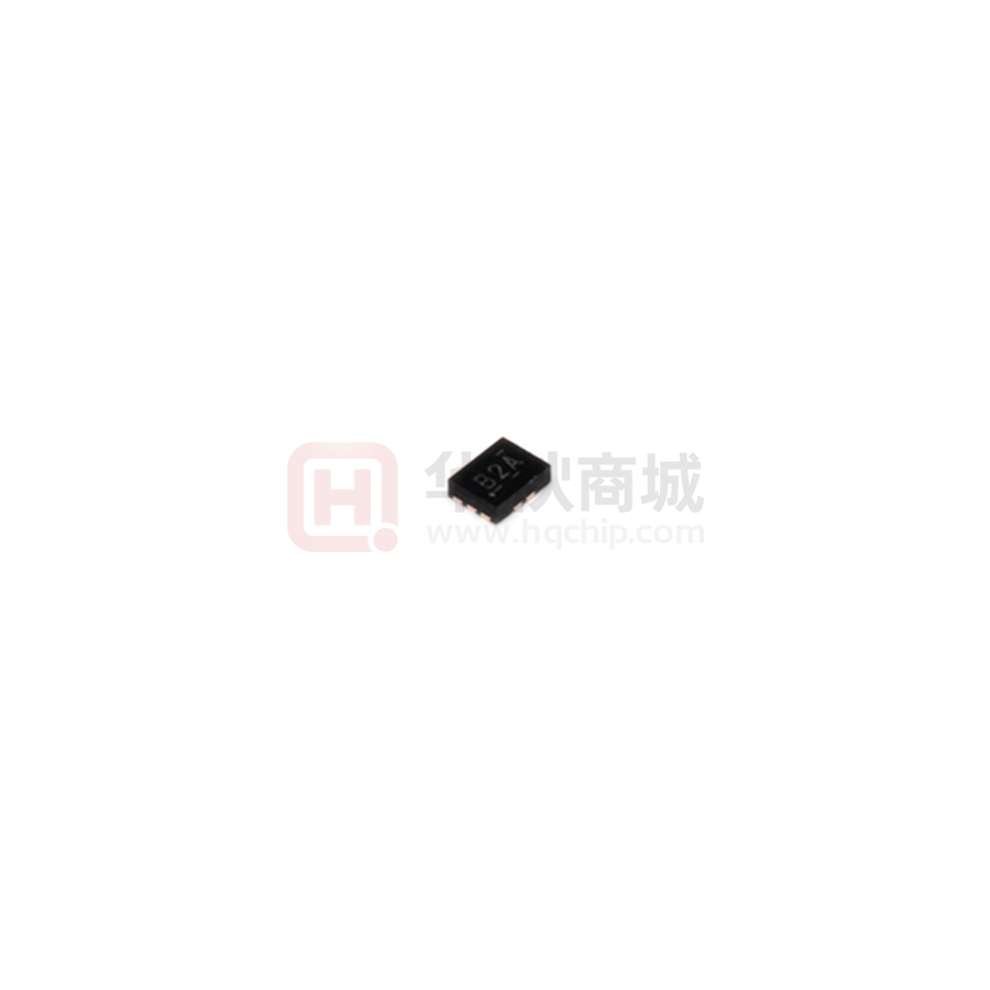
B2A
(1)
The marketing status values are defined as follows:
ACTIVE: Product device recommended for new designs.
LIFEBUY: TI has announced that the device will be discontinued, and a lifetime-buy period is in effect.
NRND: Not recommended for new designs. Device is in production to support existing customers, but TI does not recommend using this part in a new design.
PREVIEW: Device has been announced but is not in production. Samples may or may not be available.
OBSOLETE: TI has discontinued the production of the device.
(2)
RoHS: TI defines "RoHS" to mean semiconductor products that are compliant with the current EU RoHS requirements for all 10 RoHS substances, including the requirement that RoHS substance
do not exceed 0.1% by weight in homogeneous materials. Where designed to be soldered at high temperatures, "RoHS" products are suitable for use in specified lead-free processes. TI may
reference these types of products as "Pb-Free".
RoHS Exempt: TI defines "RoHS Exempt" to mean products that contain lead but are compliant with EU RoHS pursuant to a specific EU RoHS exemption.
Green: TI defines "Green" to mean the content of Chlorine (Cl) and Bromine (Br) based flame retardants meet JS709B low halogen requirements of


 工商网监
湘ICP备2023018690号
工商网监
湘ICP备2023018690号

