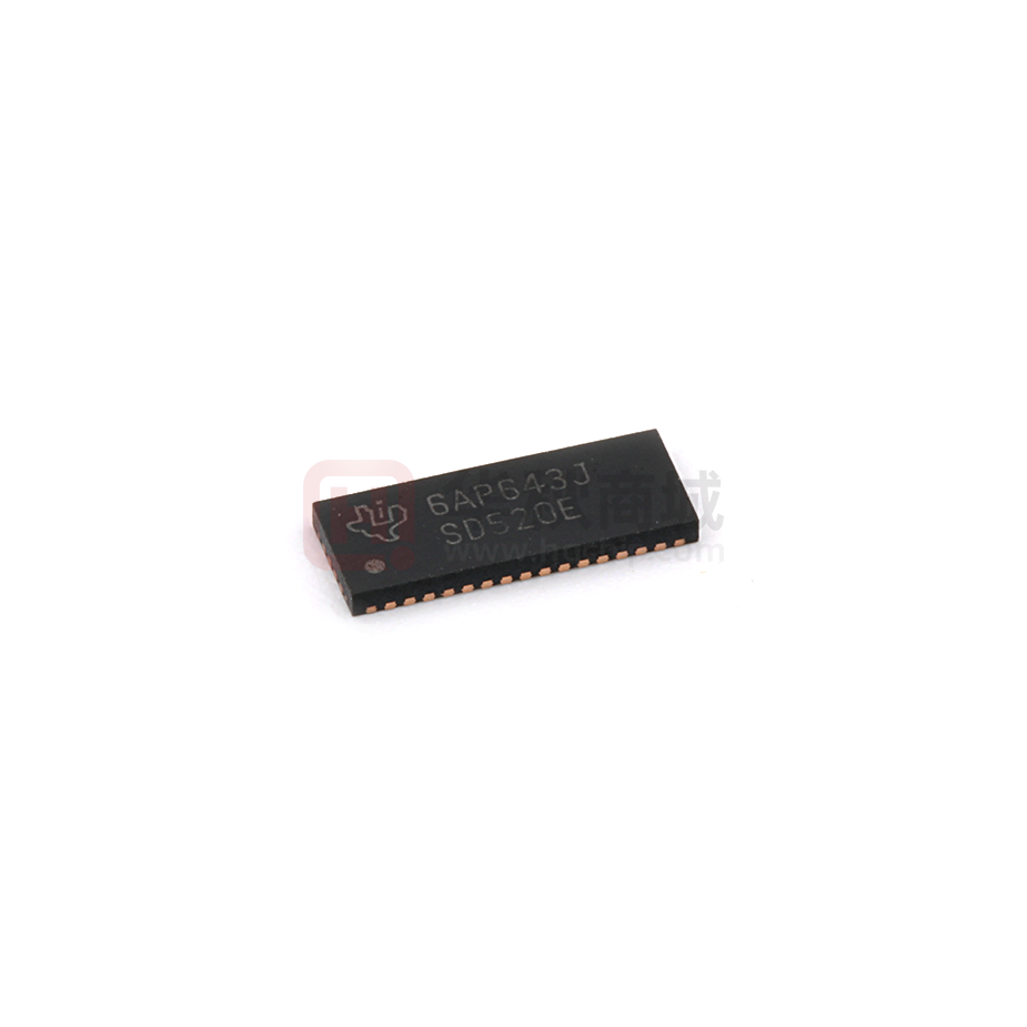
TS3DV520E
www.ti.com............................................................................................................................................................... SCDS240B – JUNE 2007 – REVISED MAY 2009
5-CHANNEL DIFFERENTIAL 10:20 MULTIPLEXER SWITCH
FOR DVI/HDMI APPLICATIONS
FEATURES
1
•
•
•
•
•
•
Compatible With HDMI v1.2a (Type A) DVI 1.0
High-Speed Digital Interface
– Wide Bandwidth to support throughput of
over 1.65 Gbps (Data rate 1.9 Gbps Typ)
– Serial Data Stream at 10× Pixel Clock Rate
– Supports All Video Formats up to 1080p
and SXGA (1280 × 1024 at 75 Hz)
– Total Raw Capacity 4.95 Gbps (Single Link)
– HDCP Compatible
Compatible with SXGA Video Display formats
up to 1080P (1280 × 1024 at 75Hz)
Low Crosstalk (XTALK = –37 dB Typ)
Low Bit-to-Bit Skew (tsk(o) = 0.1 ns Max)
Low and Flat ON-State Resistance
(ron = 4 Ω Typ, ron(flat) = 0.5 Ω Typ)
Low Input/Output Capacitance
(CON = 8 pF Typ)
•
•
•
•
Rail-to-Rail Switching on Data I/O Ports
(0 to 3.6 V)
VCC Operating Range From 3 V to 3.6 V
Latch-Up Performance Exceeds 100 mA Per
JESD 78, Class II
ESD Performance Tested
– 14-kV Human-Body Model Per JESD 22
(A114-B, Class II)
– 7.5-kV Contact Discharge Per IEC 61000-4-2
APPLICATIONS
•
•
DVI/HDMI Signal Switching
Differential DVI, HDMI Signal Multiplexing for
Audio/Video Receivers and High-Definition
Televisions (HDTVs)
DESCRIPTION/ORDERING INFORMATION
The TS3DV520E is a 20-bit to 10-bit multiplexer/demultiplexer digital video switch with a single select (SEL)
input. SEL controls the data path of the multiplexer/demultiplexer. The device provides five differential channels
for digital video signal switching.
This device provides low and flat ON-state resistance (ron) and excellent ON-state resistance match. Low
input/output capacitance, high bandwidth, low skew, and low crosstalk among channels make this device suitable
for various digital video applications, such as DVI and HDMI.
Voltage on the SEL pin should be less or equal to VCC, even in the power-down mode (VCC = 0 V).
ORDERING INFORMATION
PACKAGE (1) (2)
TA
–40°C to 85°C
(1)
(2)
ORDERABLE PART NUMBER
TOP-SIDE MARKING
TQFN – RHU
Reel of 2000
TS3DV520ERHURG4
SD520E
QFN – RUA
Reel of 2000
TS3DV520ERUAR
SD520E
Package drawings, thermal data, and symbolization are available at www.ti.com/packaging.
For the most current package and ordering information, see the Package Option Addendum at the end of this document, or see the TI
website at www.ti.com.
1
Please be aware that an important notice concerning availability, standard warranty, and use in critical applications of Texas
Instruments semiconductor products and disclaimers thereto appears at the end of this data sheet.
PRODUCTION DATA information is current as of publication date.
Products conform to specifications per the terms of the Texas
Instruments standard warranty. Production processing does not
necessarily include testing of all parameters.
Copyright © 2007–2009, Texas Instruments Incorporated
�TS3DV520E
SCDS240B – JUNE 2007 – REVISED MAY 2009............................................................................................................................................................... www.ti.com
46
4
45
5
44
6
43
7
42
8
41
9
40
Exposed
Center
Pad
12
39
38
37
36
13
14
35
15
34
16
33
17
32
18
31
0B1
A0
2
37
0B2
A1
3
36
1B2
VCC
4
35
2B1
A2
5
34
3B1
A3
6
33
2B2
VCC
7
32
3B2
A4
8
A5
9
A6
10
A7
11
SEL
VCC
A8
A9
31
VCC
30
4B1
29
5B1
28
4B2
12
27
5B2
13
26
6B1
14
25
7B1
15
24
6B2
8B1
16
23
7B2
N.C.
17
22
VCC
GND
6B1
7B1
6B2
7B2
28
27
26
1B1
Exposed
Center
Pad
18 19 20 21
9B1
GND
8B1
9B1
GND
8B2
9B2
VCC
GND
24
29
25
20
23
30
21
19
38
The exposed center pad, if used, must be
connected to GND or left electrically open.
9B2
3
1
8B2
47
VCC
0B1
1B1
0B2
1B2
GND
2B1
3B1
2B2
3B2
GND
VCC
4B1
5B1
4B2
5B2
N.C.
2
11
VCC
N.C.
42 41 40 39
48
10
N.C.
GND
49
51
50
52
53
GND
N.C.
GND
N.C.
N.C.
VCC
54
VCC
56
RUA PACKAGE
(TOP VIEW)
1
22
GND
A0
A1
VCC
N.C.
GND
A2
A3
GND
VCC
A4
A5
GND
A6
A7
GND
SEL
VCC
A8
A9
55
RHU PACKAGE
(TOP VIEW)
The exposed center pad must be connected
to GND for proper device operation.
N.C. – No internal connection
FUNCTION TABLE
INPUT
SEL
INPUT/OUTPUT
An
L
nB1
An = nB1
nB2 high-impedance mode
H
nB2
An = nB2
nB1 high-impedance mode
FUNCTION
PIN DESCRIPTION
2
NAME
DESCRIPTION
An
Data I/O
nBm
Data I/O
SEL
Select input
Submit Documentation Feedback
Copyright © 2007–2009, Texas Instruments Incorporated
Product Folder Link(s): TS3DV520E
�TS3DV520E
www.ti.com............................................................................................................................................................... SCDS240B – JUNE 2007 – REVISED MAY 2009
DVD Player
Digital TV
TS3DV520E
STB
HDMI
Receiver
Submit Documentation Feedback
Copyright © 2007–2009, Texas Instruments Incorporated
Product Folder Link(s): TS3DV520E
3
�TS3DV520E
SCDS240B – JUNE 2007 – REVISED MAY 2009............................................................................................................................................................... www.ti.com
LOGIC DIAGRAM (POSITIVE LOGIC)
2
48
3
47
0B1
A0
1B1
A1
46
0B2
45
1B2
7
43
2B1
A2
8
42
3B1
A3
41
2B2
40
3B2
11
37
4B1
A4
12
36
5B1
A5
35
4B2
34
5B2
14
32
15
31
6B1
A6
7B1
A7
30
6B2
29
7B2
19
22
8B1
A8
20
23
9B1
A9
25
8B2
26
9B2
SEL
4
17
Submit Documentation Feedback
Copyright © 2007–2009, Texas Instruments Incorporated
Product Folder Link(s): TS3DV520E
�TS3DV520E
www.ti.com............................................................................................................................................................... SCDS240B – JUNE 2007 – REVISED MAY 2009
ABSOLUTE MAXIMUM RATINGS (1)
over operating free-air temperature range (unless otherwise noted)
MIN
MAX
VCC
Supply voltage range
–0.5
4.6
V
VIN
Control input voltage range (2) (3)
–0.5
VCC + 0.5
V
(2) (3) (4)
UNIT
VI/O
Switch I/O voltage range
–0.5
VCC + 0.5
IIK
Control input clamp current
VIN < 0 or VIN > VCC
–50
50
mA
II/OK
I/O port clamp current
VI/O < 0 or VI/O > VCC
–50
50
mA
±128
mA
±100
mA
II/O
ON-state switch current
(5)
Continuous current through VCC or GND
θJA
Package thermal impedance (6)
Tstg
Storage temperature range
(1)
(2)
(3)
(4)
(5)
(6)
RHU package
31.8
RUA package
51.2
–65
150
V
°C/W
°C
Stresses beyond those listed under "absolute maximum ratings" may cause permanent damage to the device. These are stress ratings
only, and functional operation of the device at these or any other conditions beyond those indicated under "recommended operating
conditions" is not implied. Exposure to absolute-maximum-rated conditions for extended periods may affect device reliability.
All voltages are with respect to ground, unless otherwise specified.
The input and output voltage ratings may be exceeded if the input and output clamp-current ratings are observed.
VI and VO are used to denote specific conditions for VI/O.
II and IO are used to denote specific conditions for II/O.
The package thermal impedance is calculated in accordance with JESD 51-7.
RECOMMENDED OPERATING CONDITIONS (1)
MIN
MAX
UNIT
VCC
Supply voltage
3
3.6
V
VIH
High-level control input voltage (SEL)
2
VCC
V
VIL
Low-level control input voltage (SEL)
0
0.8
V
VI/O
Input/output voltage
0
VCC
V
TA
Operating free-air temperature
–40
85
°C
(1)
All unused control inputs of the device must be held at VCC or GND to ensure proper device operation. Refer to the TI application report,
Implications of Slow or Floating CMOS Inputs, literature number SCBA004.
Submit Documentation Feedback
Copyright © 2007–2009, Texas Instruments Incorporated
Product Folder Link(s): TS3DV520E
5
�TS3DV520E
SCDS240B – JUNE 2007 – REVISED MAY 2009............................................................................................................................................................... www.ti.com
ELECTRICAL CHARACTERISTICS (1)
for high-frequency switching over recommended operating free-air temperature range, VCC = 3.3 V ± 0.3 V
(unless otherwise noted)
PARAMETER
TEST CONDITIONS
MIN
TYP (2)
MAX
–0.7
–1.2
V
UNIT
VIK
SEL
VCC = 3.6 V,
IIN = –18 mA
IIH
SEL
VCC = 3.6 V,
VIN = VCC
±1
µA
IIL
SEL
VCC = 3.6 V,
VIN = GND
±1
µA
250
600
µA
2
2.5
pF
ICC
VCC = 3.6 V,
II/O = 0,
CIN
SEL
f = 1 MHz,
VIN = 0
COFF
B port
VI = 0,
f = 1 MHz,
Outputs open,
Switch OFF
3
4
pF
CON
VI = 0,
f = 1 MHz,
Outputs open,
Switch ON
9
9.8
pF
ron
VCC = 3 V,
1.5 V ≤ VI ≤ VCC,
IO = –40 mA
4
8
Ω
ron(flat) (3)
VCC = 3 V,
VI = 1.5 V and VCC,
IO = –40 mA
0.7
VCC = 3 V,
1.5 V ≤ VI ≤ VCC,
IO = –40 mA
0.2
Δron
(1)
(2)
(3)
(4)
(4)
Switch ON or OFF
Ω
1.2
Ω
VI, VO, II, and IO refer to I/O pins. VIN refers to the control inputs.
All typical values are at VCC = 3.3 V (unless otherwise noted), TA = 25°C.
ron(flat) is the difference of ron in a given channel at specified voltages.
Δron is the difference of ron from center (A4, A5) ports to any other port.
SWITCHING CHARACTERISTICS
over recommended operating free-air temperature range, VCC = 3.3 V ± 0.3 V, RL = 200 Ω, CL = 10 pF
(unless otherwise noted) (see Figure 5 and Figure 6)
PARAMETER
FROM
(INPUT)
TO
(OUTPUT)
tpd (2)
A or B
B or A
tPZH, tPZL
SEL
A or B
0.5
15
ns
tPHZ, tPLZ
SEL
A or B
0.5
9
ns
A or B
B or A
0.05
0.1
ns
0.05
0.1
ns
tsk(o)
(3)
MIN
TYP (1)
0.25
tsk(p) (4)
(1)
(2)
(3)
(4)
MAX
UNIT
ns
All typical values are at VCC = 3.3 V (unless otherwise noted), TA = 25°C.
The propagation delay is the calculated RC time constant of the typical ON-state resistance of the switch and the specified load
capacitance when driven by an ideal voltage source (zero output impedance).
Output skew between center port (A4 to A5) to any other port
Skew between opposite transitions of the same output in a given device |tPHL – tPLH|
DYNAMIC CHARACTERISTICS
over recommended operating free-air temperature range, VCC = 3.3 V ± 0.3 V (unless otherwise noted)
PARAMETER
(1)
6
TEST CONDITIONS
TYP (1)
UNIT
XTALK
RL = 100 Ω,
f = 250 MHz,
See Figure 8
–37
dB
OIRR
RL = 100 Ω,
f = 250 MHz,
See Figure 9
–37
dB
BW
RL = 100 Ω,
See Figure 7
950
MHz
All typical values are at VCC = 3.3 V (unless otherwise noted), TA = 25°C.
Submit Documentation Feedback
Copyright © 2007–2009, Texas Instruments Incorporated
Product Folder Link(s): TS3DV520E
�TS3DV520E
www.ti.com............................................................................................................................................................... SCDS240B – JUNE 2007 – REVISED MAY 2009
OPERATING CHARACTERISTICS
0
0
−2
Attenuation (dB)
−20
Gain (dB)
−4
−6
−8
−40
−60
−80
−10
−12
0.1
1
10
100
1000
10,000
−100
0.1
1
Frequency (MHz)
Figure 1. Gain/Phase vs Frequency
10,000
Figure 2. OFF Isolation vs Frequency
6
0
5
−20
4
−40
ron (Ω)
Attenuation (dB)
1000
10
100
Frequency (MHz)
3
−60
2
−80
−100
0.1
1
0
1
10
100
Frequency (MHz)
1000
10,000
0
1
2
3
4
5
6
VCOM (V)
Figure 3. Crosstalk vs Frequency
Figure 4. ron vs VCOM (VCC = 3.6 V
Submit Documentation Feedback
Copyright © 2007–2009, Texas Instruments Incorporated
Product Folder Link(s): TS3DV520E
7
�TS3DV520E
SCDS240B – JUNE 2007 – REVISED MAY 2009............................................................................................................................................................... www.ti.com
APPLICATION INFORMATION
TMDS Data 2+
TMDS Data 2–
2
48
A1
3
47
1B1
46
0B2
4
45
1B2
6
TMDS Data 1+
A2
7
TMDS Data 1–
A3
8
0B1
2B1
3B1
41
2B2
10
40
3B2
12
11
37
4B1
TMDS Data 0–
A5
12
36
5B1
35
4B2
34
5B2
32
6B1
31
7B1
30
6B2
29
TMDS Clock+
A6
TMDS Clock–
A7
15
To HDMI Receiver
7
42
A4
14
3
43
TMDS Data 0+
9
TMDS Data 2+
TMDS Data 2–
TMDS Data 1+
TMDS Data 1–
TMDS Data 0+
TMDS Data 0–
TMDS Clock+
TMDS Clock–
HDMI Connector 1
(Single Link)
1
TMDS Data 2+
7B2
3
TMDS Data 2–
A8
19
22
8B1
4
A9
20
23
9B1
6
25
8B2
7
9B2
9
26
SEL
1
A0
10
20
12
TS3DV520E
TMDS Data 1+
TMDS Data 1–
TMDS Data 0+
TMDS Data 0–
TMDS Clock+
TMDS Clock–
HDMI Connector 2
(Single Link)
Typical HDMI Connector
Pin Signal Assignment
Pin 19
Pin 1
1
TMDS Data 2+
2
3
TMDS Data 2 Shield
TMDS Data 2–
4
TMDS Data 1+
5
TMDS Data 1 Shield
6
TMDS Data 1–
7
TMDS Data 0+
8
TMDS Data 0 Shield
9
TMDS Data 0–
10
TMDS Clock+
11
TMDS Clock Shield
12
TMDS Clock–
13
CEC
14
Reserved (N.C. on device)
15
SCL
16
SDA
17
DDC/CEC Ground
18
5 V Power
19
Hot Plug Detect
The TS3DV520E can be used to switch
between two digital video ports.
8
Submit Documentation Feedback
Copyright © 2007–2009, Texas Instruments Incorporated
Product Folder Link(s): TS3DV520E
�TS3DV520E
www.ti.com............................................................................................................................................................... SCDS240B – JUNE 2007 – REVISED MAY 2009
PARAMETER MEASUREMENT INFORMATION
(Enable and Disable Times)
VCC
Input Generator
VIN
50 Ω
50 Ω
VG1
TEST CIRCUIT
DUT
2 × VCC
Input Generator
VI
S1
RL
VO
Open
GND
50 Ω
CL
(see Note A)
50 Ω
VG2
RL
TEST
VCC
S1
RL
VI
CL
V∆
tPLZ/tPZL
3.3 V ± 0.3 V
2 × VCC
200 Ω
GND
10 pF
0.3 V
tPHZ/tPZH
3.3 V ± 0.3 V
GND
200 Ω
VCC
10 pF
0.3 V
2.5 V
Output Control
(VIN)
1.25 V
1.25 V
0V
Output
Waveform 1
S1 at 2 y VCC
(see Note B)
tPZL
tPLZ
VOH
VCC/2
tPZH
Output
Waveform 2
S1 at GND
(see Note B)
VOL +0.3 V
VOL
tPHZ
VCC/2
VOH −0.3 V
VOH
VOL
VOLTAGE WAVEFORMS
ENABLE AND DISABLE TIMES
NOTES: A. CL includes probe and jig capacitance.
B. Waveform 1 is for an output with internal conditions such that the output is low, except when disabled by the output control.
Waveform 2 is for an output with internal conditions such that the output is high, except when disabled by the output control.
C. All input pulses are supplied by generators having the following characteristics: PRR ≤ 10 MHz, ZO = 50 Ω, tr ≤ 2.5 ns, tf ≤ 2.5 ns.
D. The outputs are measured one at a time, with one transition per measurement.
E. tPLZ and tPHZ are the same as tdis.
F. tPZL and tPZH are the same as ten.
Figure 5. Test Circuit and Voltage Waveforms
Submit Documentation Feedback
Copyright © 2007–2009, Texas Instruments Incorporated
Product Folder Link(s): TS3DV520E
9
�TS3DV520E
SCDS240B – JUNE 2007 – REVISED MAY 2009............................................................................................................................................................... www.ti.com
PARAMETER MEASUREMENT INFORMATION
(Skew)
VCC
Input Generator
VIN
50 Ω
50 Ω
VG1
TEST CIRCUIT
DUT
2 × VCC
Input Generator
S1
RL
VO
VI
Open
GND
50 Ω
CL
(see Note A)
50 Ω
VG2
RL
TEST
VCC
S1
RL
VI
CL
tsk(o)
3.3 V ± 0.3 V
Open
200 Ω
VCC or GND
10 pF
tsk(p)
3.3 V ± 0.3 V
Open
200 Ω
VCC or GND
10 pF
V∆
3.5 V
2.5 V
1.5 V
Data In at
Ax or Ay
tPLHx
tPHLx
VOH
(VOH + VOL)/2
VOL
Data Out at
XB1 or XB2
tsk(o)
2.5 V
1.5 V
Input
tsk(o)
VOH
(VOH + VOL)/2
VOL
Data Out at
YB1 or YB2
tPLHy
3.5 V
tPHLy
tPLH
tPHL
VOH
(VOH + VOL)/2
VOL
Output
tsk(p) = |tPLH − tPLH|
tsk(o) = |tPLHy − tPLHx| or |tPHLy − tPHLx|
VOLTAGE WAVEFORMS
OUTPUT SKEW (tsk(o))
VOLTAGE WAVEFORMS
PULSE SKEW (tsk(p))
NOTES: A. CL includes probe and jig capacitance.
B. Waveform 1 is for an output with internal conditions such that the output is low, except when disabled by the output control.
Waveform 2 is for an output with internal conditions such that the output is high, except when disabled by the output control.
C. All input pulses are supplied by generators having the following characteristics: PRR ≤ 10 MHz, ZO = 50 Ω, tr ≤ 2.5 ns, tf ≤ 2.5 ns.
D. The outputs are measured one at a time, with one transition per measurement.
Figure 6. Test Circuit and Voltage Waveforms
10
Submit Documentation Feedback
Copyright © 2007–2009, Texas Instruments Incorporated
Product Folder Link(s): TS3DV520E
�TS3DV520E
www.ti.com............................................................................................................................................................... SCDS240B – JUNE 2007 – REVISED MAY 2009
PARAMETER MEASUREMENT INFORMATION
EXT TRIGGER
BIAS
VBIAS
Network Analyzer
(HP8753ES)
P1
P2
VCC
A0
0B1
CL = 10 pF
SEL
DUT
VSEL
Figure 7. Test Circuit for Frequency Response (BW)
Frequency response is measured at the output of the ON channel. For example, when VSEL = 0 and A0 is the
input, the output is measured at 0B1. All unused analog I/O ports are left open.
HP8753ES setup
Average = 4
RBW = 3 kHz
VBIAS = 0.35 V
ST = 2 s
P1 = 0 dBM
Submit Documentation Feedback
Copyright © 2007–2009, Texas Instruments Incorporated
Product Folder Link(s): TS3DV520E
11
�TS3DV520E
SCDS240B – JUNE 2007 – REVISED MAY 2009............................................................................................................................................................... www.ti.com
PARAMETER MEASUREMENT INFORMATION
EXT TRIGGER
BIAS
VBIAS
Network Analyzer
(HP8753ES)
P1
P2
VCC
0B1
A0
RL = 100 Ω
A1
1B1
0B2
DUT
A2
1B2
2B1
RL = 100 Ω
A3
3B1
2B2
3B2
SEL
VSEL
A.
A 50-Ω termination resistor is needed to match the loading of the network analyzer.
Figure 8. Test Circuit for Crosstalk (XTALK)
Crosstalk is measured at the output of the nonadjacent ON channel. For example, when VSEL = 0 and A0 is the
input, the output is measured at 1B1. All unused analog input (A) ports are connected to GND, and output (B)
ports are connected to GND through 50-Ω pulldown resistors.
HP8753ES setup
Average = 4
RBW = 3 kHz
VBIAS = 0.35 V
ST = 2 s
P1 = 0 dBM
12
Submit Documentation Feedback
Copyright © 2007–2009, Texas Instruments Incorporated
Product Folder Link(s): TS3DV520E
�TS3DV520E
www.ti.com............................................................................................................................................................... SCDS240B – JUNE 2007 – REVISED MAY 2009
PARAMETER MEASUREMENT INFORMATION
EXT TRIGGER
BIAS
VBIAS
Network Analyzer
(HP8753ES)
P1
P2
VCC
0B1
A0
RL = 100 Ω
A1
1B1
DUT
0B2
1B2
SEL
VSEL
A.
A 50-Ω termination resistor is needed to match the loading of the network analyzer.
Figure 9. Test Circuit for OFF Isolation (OIRR)
OFF isolation is measured at the output of the OFF channel. For example, when VSEL = VCC and A0 is the input,
the output is measured at 0B2. All unused analog input (A) ports are left open, and output (B) ports are
connected to GND through 50-Ω pulldown resistors.
HP8753ES setup
Average = 4
RBW = 3 kHz
VBIAS = 0.35 V
ST = 2
P1 = 0 dBM
Submit Documentation Feedback
Copyright © 2007–2009, Texas Instruments Incorporated
Product Folder Link(s): TS3DV520E
13
�PACKAGE OPTION ADDENDUM
www.ti.com
24-Aug-2018
PACKAGING INFORMATION
Orderable Device
Status
(1)
TS3DV520ERUAR
ACTIVE
Package Type Package Pins Package
Drawing
Qty
WQFN
RUA
42
3000
Eco Plan
Lead/Ball Finish
MSL Peak Temp
(2)
(6)
(3)
Green (RoHS
& no Sb/Br)
CU NIPDAUAG
Level-1-260C-UNLIM
Op Temp (°C)
Device Marking
(4/5)
-40 to 85
SD520E
(1)
The marketing status values are defined as follows:
ACTIVE: Product device recommended for new designs.
LIFEBUY: TI has announced that the device will be discontinued, and a lifetime-buy period is in effect.
NRND: Not recommended for new designs. Device is in production to support existing customers, but TI does not recommend using this part in a new design.
PREVIEW: Device has been announced but is not in production. Samples may or may not be available.
OBSOLETE: TI has discontinued the production of the device.
(2)
RoHS: TI defines "RoHS" to mean semiconductor products that are compliant with the current EU RoHS requirements for all 10 RoHS substances, including the requirement that RoHS substance
do not exceed 0.1% by weight in homogeneous materials. Where designed to be soldered at high temperatures, "RoHS" products are suitable for use in specified lead-free processes. TI may
reference these types of products as "Pb-Free".
RoHS Exempt: TI defines "RoHS Exempt" to mean products that contain lead but are compliant with EU RoHS pursuant to a specific EU RoHS exemption.
Green: TI defines "Green" to mean the content of Chlorine (Cl) and Bromine (Br) based flame retardants meet JS709B low halogen requirements of


 工商网监
湘ICP备2023018690号
工商网监
湘ICP备2023018690号
