�����������
��
����� ����
��
�
��
� � ����
SGLS120B − APRIL 2002 − REVISED APRIL 2008
D
D
D
D
D
MIL-STD-883, Method 3015; Exceeds 200 V
Using Machine Model (CL = 200 pF, RL = 0)
2.7-V Operation
Two Differential Microphone Inputs, One
Differential Earphone Output, and One
Single-Ended Earphone Output
Programmable Gain Amplifiers for
Transmit, Receive, Sidetone, and Volume
Control
Earphone Mute and Microphone Mute
On-Chip I2C Bus, Which Provides a Simple,
Standard, Two-Wire Serial Interface With
Digital ICs
D Programmable for 15-Bit Linear Data or
D
D
D
D
8-Bit Companded (µ-Law or A-Law) Data
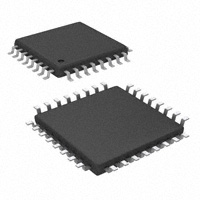
Available in a 32-Pin Thin Quad Flatpack
(TQFP) Package
Designed for Analog and Digital Wireless
Handsets and Telecommunications
Applications
Dual-Tone Multifrequency (DTMF) and
Single Tone Generator
Pulse Density Modulated (PDM) Buzzer
Output
PBS PACKAGE
(TOP VIEW)
PLLVSS
VSS
MCLK
RESET
PWRUPSEL
BUZZCON
PCMSYN
PCMCLK
D Qualified for Automotive Applications
D ESD Protection Exceeds 2000 V Per
description
The voice-band audio processor (VBAP) is
designed to perform transmit encoding analog/
digital (A/D) conversion, receive decoding
digital/analog (D/A) conversion, and transmit and
receive filtering for voice-band communications
systems. The device operates in either the 15-bit
linear or 8-bit companded (µ-law or A-Law) mode,
which is selectable through the I2C interface. The
VBAP generates its own internal clocks from a
2.048-MHz master clock input.
AVAILABLE OPTIONS{
24 23 22 21 20 19 18 17
PLLVDD
EARVSS
EAR1ON
EARVDD
EAR1OP
EARVSS
EAR2O
AVDD
16
25
PCMO
PCMI
DVSS
DVDD
12 SCL
11 SDA
10 NC
9 NC
26
15
14
13
27
28
29
30
31
32
TA
PART NO.
TOP-SIDE
MARKING
−40°C to
105°C
Tube
Tape and Reel
TWL1103TPBSQ1
TWL1103TPBSRQ1
TWL1103T
TWL1103T
† For the most current package and ordering information, see the
Package Option Addendum at the end of this document, or see the TI
web site at http://www.ti.com.
‡ Package drawings, thermal data, and symbolization are available at
http://www.ti.com/packaging.
2
3
4 5 6 7
8
MBIAS
MIC1P
MIC1N
MIC2P
MIC2N
REXT
NC
AVSS
1
TQFP PBS
PACKAGE}
NC − No internal connection
VBAP is a trademark of Texas Instruments.
All other trademarks are the property of their respective owners.
Copyright 2008, Texas Instruments Incorporated
��
�����
� ���� ����������� �! "#��$�� �! �� %#&'�"����� (��$)
���(#"�! "������ �� !%$"���"�����! %$� �*$ �$��! �� �$+�! ��!��#�$��!
!���(��( ,������-) ���(#"���� %��"$!!��. (�$! ��� �$"$!!���'- ��"'#($
�$!���. �� �'' %����$�$�!)
POST OFFICE BOX 655303
• DALLAS, TEXAS 75265
1
������������
��
����� ����
��
�
��
� � ����
SGLS120B − APRIL 2002 − REVISED APRIL 2008
functional block diagram
PCMO (16)
EAR1OP (29) EAR1ON (27) EAR2O (31)
Ear
Amp1
BUZZCON (19)
Ear
Amp2
PWRUPSEL (20)
Digital
Modulator
and Filter
Buzzer
Control
Power
and
RESET
V SS
(23)
AV DD
(32)
AV SS
(8)
DV DD
(13)
DV SS
(14)
PLLV DD (25)
PLLV SS (24)
EARV DD (28)
RX Filter
and PGA
g = −6 dB
to +6 dB
EARV SS (30, 26)
RESET
(21)
RX
Volume Control
g = −18 dB
to 0 dB
PLL
MCLK (22)
Sidetone
g = −24 dB
to
−12 dB
PCM
Interface
DTMF
Generator
TX Filter
and PGA
g = −10 dB
to 0 dB
REF
REXT (6)
MBIAS (1)
Analog
Modulator
Control Bus
MIC
Amplifier 2
g = 12 dB
or 0 dB
I 2C
I/F
MIC
Amplifier
1g =
23.5 dB
PCMCLK (17)
PCMI (15)
PCMSYN (18)
MIC1P (2)
2
MIC1N (3)
MIC2P (4)
POST OFFICE BOX 655303
MIC2N (5)
• DALLAS, TEXAS 75265
SDA
(11)
SCL
(12)
������������
��
����� ����
��
�
��
� � ����
SGLS120B − APRIL 2002 − REVISED APRIL 2008
functional description
power on/reset
The power for the various digital and analog circuits is separated to improve the noise performance of the
device. An external reset must be applied to the active low RESET terminal to guarantee reset upon power on.
After the initial power-on sequence the TWL1103 can be functionally powered up and down by writing to the
power control register through the I2C interface. There is a hardwired selectable power-up terminal in default
mode option. The PWRUPSEL function allows the VBAP to power up in the default mode and allows use without
a microcontroller.
reference
A precision band gap reference voltage is generated internally and supplies all required voltage references to
operate the transmit and receive channels. The reference system also supplies bias voltage for use with an
electret microphone at terminal MBIAS. An external precision resistor is required for reference current setting
at terminal REXT.
control interface
The I2C interface is a two-wire bidirectional serial interface that controls the VBAP by writing data to the six
control registers:
D
D
D
D
D
D
Power control
Mode control
Transmit PGA and sidetone control
Receive PGA gain and volume control
DTMF high tone
DTMF low tone
There are two power-up modes which may be selected at the PWRUPSEL terminal:
D The PWRUPSEL state (VDD at terminal 20) causes the device to power up in the default mode when power
is applied. In the default mode, the I2C interface is not required, and the device may be used without an I2C
interface. The programmable functions are fixed in the default modes.
D The PWRUPSEL state (ground at terminal 20) causes the device to go to a power-down state when power
is applied. In this mode an I2C interface is required to power up the device.
phase-locked loop
The internal digital filters and modulators require a 10.24-MHz clock that is generated by phase locking to the
2.048-MHz master clock input.
PCM interface
The PCM interface transmits and receives data at the PCMO and PCMI terminals respectively. The data is
transmitted or received at the PCMCLK speed once every PCMSYN cycle. The PCMCLK can be tied directly
to the 2.048-MHz master clock (MCLK). The PCMSYN can be driven by an external source or derived from the
master clock and used as an interrupt to the host controller.
microphone amplifiers
The microphone input is a switchable interface for two differential microphone inputs. The first stage is a lownoise differential amplifier that provides a gain of 23.5 dB. The second stage amplifier has a selectable gain of
0 dB or 12 dB.
POST OFFICE BOX 655303
• DALLAS, TEXAS 75265
3
������������
��
����� ����
��
�
��
� � ����
SGLS120B − APRIL 2002 − REVISED APRIL 2008
functional description (continued)
analog modulator
The transmit channel modulator is a third-order sigma-delta design.
transmit filter and PGA
The transmit filter is a digital filter designed to meet CCITT G.714 requirements. The device operates in either
the 15-bit linear or 8-bit companded µ-law or A-law mode that is selectable through the I2C interface. The
transmit PGA defaults to 0 dB.
sidetone
A portion of the transmitted audio is attenuated and fed back to the receive channel through the sidetone path.
The sidetone path defaults to −12 dB. The sidetone path can be enabled by writing to the power control register.
receive volume control
The receive volume control block acts as an attenuator with a range of −18 dB to 0 dB in 2 dB steps for control
of the receive channel volume. The receive volume control gain defaults to 0 dB.
receive filter and PGA
The receive filter is a digital filter that meets CCITT G.714 requirements with a high-pass filter that is selectable
through the I2C interface. The device operates in either the 15-bit linear or 8-bit µ-law or A-law companded
mode, which is selectable through the I2C interface. The gain defaults to −1 dB representing a 3-dBm0 level
for a 32-Ω load impedance and the corresponding digital full scale PCMI code. The gain may be set to −2 dB
for the respective 3-dBm0 level for a 16-Ω load impedance.
digital modulator and filter
The second-order digital modulator and filter convert the received digital PCM data to the analog output required
by the earphone interface.
earphone amplifiers
The analog signal can be routed to either of two earphone amplifiers, one with differential output (EAR1ON and
EAR1OP) and one with single-ended output (EAR2O). Clicks and pops are suppressed for EAR1 differential
output only.
tone generator
The tone generator provides generation of standard DTMF tones and single tone frequencies which are output
to the following devices: 1) The buzzer driver, as a pulse density modulation (PDM) signal 2) The receive path
digital/analog converter (DAC) for outputting through the earphone. There are 255 possible single tones. The
tone integer value is determined by the following formula:
Round (Tone Freq (Hz)/7.8135 Hz)
The value is loaded into one of two 8-bit registers, the high-tone register (04), or the low-tone register (05). The
tone output is 2 dB higher when applied to the high-tone register (04). When generating DTMF tones, the high
DTMF tone must be applied to the high-tone register and the low frequency tone to the low-tone register.
4
POST OFFICE BOX 655303
• DALLAS, TEXAS 75265
������������
��
����� ����
��
�
��
� � ����
SGLS120B − APRIL 2002 − REVISED APRIL 2008
Terminal Functions
TERMINAL
NO.
NAME
I/O
DESCRIPTION
µBGA
PBS
AVDD
AVSS
A1
32
I
Analog positive power supply
J1
8
I
Analog negative power supply
BUZZCON
F9
19
O
Buzzer output, a pulse-density modulated signal to apply to external buzzer driver
DVDD
J6
13
I
Digital positive power supply
DVSS
J7
14
I
Digital negative power supply
EAR1ON
A6
27
O
Earphone 1 amplifier output (−)
EAR1OP
A4
29
O
Earphone 1 amplifier output (+)
EAR2O
A2
31
O
Earphone 2 amplifier output
EARVDD
EARVSS
A5
28
I
Analog positive power supply for the earphone amplifiers
A3, A7
30, 26
I
Analog negative power supply for the earphone amplifiers
MBIAS
B1
1
O
Microphone bias supply output, no decoupling capacitors
MCLK
C9
22
I
Master system clock input (2.048 MHz) (digital)
MIC1P
C1
2
I
MIC1 input (+)
MIC1N
D1
3
I
MIC1 input (−)
MIC2P
E1
4
I
MIC2 input (+)
MIC2N
F1
5
I
MIC2 input (−)
PCMI
J8
15
I
Receive PCM input
PCMO
J9
16
O
Transmit PCM output
PCMSYN
G9
18
I
PCM frame synchronization
PCMCLK
H9
17
I
PCM data clock
PLLVSS
PLLVDD
A9
24
I
PLL negative power supply
A8
25
I
PLL digital power supply
PWRUPSEL
E9
20
I
Selects the power-up default mode
REXT
G1
6
I/O
RESET
D9
21
I
SCL
J5
12
I
SDA
J4
11
I/O
VSS
B9
23
I
Internal reference current setting terminal—use precision 100-kΩ resistor and no filtering capacitors
Active low reset
I2C-bus serial clock—this input is used to synchronize the data transfer from and to the VBAP
I2C-bus serial address/data input/output—this is a bidirectional terminal used to transfer register
control addresses and data into and out of the CODEC. It is an open-drain terminal and therefore
requires a pullup resistor to VDD (typical 10 kΩ for 100 kHz)
Ground return for bandgap internal reference
POST OFFICE BOX 655303
• DALLAS, TEXAS 75265
5
������������
��
����� ����
��
�
��
� � ����
SGLS120B − APRIL 2002 − REVISED APRIL 2008
absolute maximum ratings over operating free-air temperature range (unless otherwise noted)†
Supply voltage range, AVDD, DVDD, PLLVDD, EARVDD . . . . . . . . . . . . . . . . . . . . . . . . . . . . . . . . . −0.5 V to 4 V
Output voltage range, VO . . . . . . . . . . . . . . . . . . . . . . . . . . . . . . . . . . . . . . . . . . . . . . . . . . . . . . . . . . . . −0.5 V to 4 V
Input voltage range, VF . . . . . . . . . . . . . . . . . . . . . . . . . . . . . . . . . . . . . . . . . . . . . . . . . . . . . . . . . . . . . . −0.5 V to 4 V
Continuous total power dissipation . . . . . . . . . . . . . . . . . . . . . . . . . . . . . . . . . . . . . . See Dissipation Rating Table
Operating free air temperature range, TA (extended temperature) . . . . . . . . . . . . . . . . . . . . . . . −40°C to 105°C
Storage temperature range, testing, Tstg . . . . . . . . . . . . . . . . . . . . . . . . . . . . . . . . . . . . . . . . . . . . . −65°C to 150°C
Lead temperature 1,6 mm from case for 10 seconds . . . . . . . . . . . . . . . . . . . . . . . . . . . . . . . . . . . . . . . . . . 260°C
† Stresses beyond those listed under “absolute maximum ratings” may cause permanent damage to the device. These are stress ratings only, and
functional operation of the device at these or any other conditions beyond those indicated under “recommended operating conditions” is not
implied. Exposure to absolute-maximum-rated conditions for extended periods may affect device reliability.
DISSIPATION RATING TABLE
PACKAGE
TA ≤ 25°C
POWER RATING
DERATING FACTOR
ABOVE TA = 25°C
TA = 85°C
POWER RATING
TA = 105°C
POWER RATING
PBS
680 mW
6.8 mW/°C
270 mW
134 mW
recommended operating conditions (see Notes 1 and 2)
MIN
Supply voltage, AVDD, DVDD, PLLVDD, EARVDD
NOM
2.7
High-level input voltage (VIH)
MAX
UNIT
3.3
V
0.7 x VDD
V
Low-level input voltage (VIL)
Load impedance between EAR1OP and EAR1ON-RL
16
Load impedance for EAR2OP-RL
32
0.3 x VDD
V
32
Ω
Ω
Operating free-air temperature, TA
−40
105
_C
NOTES: 1. To avoid possible damage and resulting reliability problems to these CMOS devices, the power-on initialization paragraph must be
followed, described in the Principles of Operations.
2. Voltages are with respect to AVSS, DVSS, PLLVSS, and EARVSS.
6
POST OFFICE BOX 655303
• DALLAS, TEXAS 75265
������������
��
����� ����
��
�
��
� � ����
SGLS120B − APRIL 2002 − REVISED APRIL 2008
electrical characteristics, VDD = 2.7 V, TA = −40°C to 105°C (unless otherwise noted)
supply current
PARAMETER
IDD
TEST CONDITIONS
Supply current from VDD
TYP
MAX
UNIT
Operating, EAR1 selected, MicBias disabled
MIN
6
7
mA
Operating, EAR2 selected, MicBias disabled
5.4
6
mA
Power down, Reg 2 bit 7 = 1, MClk not present
(see Note 3)
0.5
18
µA
Power down, Reg 2 bit 7 = 0, MClk not present
(see Note 3)
25
40
µA
5
10
ms
TYP
MAX
UNIT
ton(i)
Power-up time from power down
NOTE 3: VIH = VDD, VIL = VSS
digital interface
PARAMETER
TEST CONDITIONS
VOH
VOL
High-level output voltage, PCMO and BuzzCon
IIH
IIL
High-level input current, any digital input
CI
Input capacitance
Co
Output capacitance
20
pF
RL
Load impedance (BuzzCon)
5
kΩ
Low-level output voltage, PCMO and BuzzCon
Low-level input current, any digital input
IOH = − 3.2 mA,
IOL = 3.2 mA,
VDD = 3 V
VDD = 3 V
MIN
2
V
VI = VDD
VI = VSS
0.8
V
10
µA
10
µA
10
pF
microphone interface
PARAMETER
TEST CONDITIONS
VIO
IIB
Input offset voltage at MIC1N, MIC2N
Ci
Input capacitance at MIC1N, MIC2N
Vn
Microphone input referred noise, psophometric weighted
(C-message weighted is similar)
IOmax
V(mbias)
See Note 4
Input bias current at MIC1N, MIC2N
MIN
TYP
MAX
5
mV
−600
600
nA
5
Micamp 1 gain = 23.5 dB
Micamp 2 gain = 0 dB
Output source current MBIAS
3.0
1
Microphone bias supply voltage (see Note 5)
2.35
2.5
MICMUTE
Input impedance
Fully differential
UNIT
−5
35
60
pF
7.7
µVrms
1.2
mA
2.6
V
−80
dB
100
kΩ
NOTES: 4. Measured while MIC1P and MIC1N are connected together. Less than 5 mV offset results in 0 value code on PCMOUT.
5. Not a JEDEC symbol.
speaker interface
PARAMETER
TEST CONDITIONS
Earphone AMP1 output power (See Note 6)
VOO
IOmax
TYP
MAX
UNIT
VDD = 2.7 V, fully differential, 16-Ω load,
3-dBm0 output, RGXPA = − 2 dB
MIN
120.9
151.1
mW
VDD = 2.7 V, fully differential, 32-Ω load,
3-dBm0 output, RGXPA = −1 dB
76.1
95.1
mW
Earphone AMP2 output power (See Note 6)
VDD = 2.7 V, single ended, 32-Ω load,
3-dBm0 output
10
12.5
mW
Output offset voltage at EAR1
Fully differential
±5
±30
mV
3-dBm0 input, 16-Ω load
86.9
108.6
3-dBm0 input, 32-Ω load
48.7
60.8
3-dBm0 input
17.7
22.1
Maximum output current for EAR1(rms)
Maximum output current for EAR2 (rms)
EARMUTE
−80
mA
dB
NOTE 6: Maximum power is with a load impedance of approximately 12 Ω.
POST OFFICE BOX 655303
• DALLAS, TEXAS 75265
7
������������
��
����� ����
��
�
��
� � ����
SGLS120B − APRIL 2002 − REVISED APRIL 2008
electrical characteristics, VDD = 2.7 V, TA = −40°C to 105°C (unless otherwise noted) (continued)
transmit gain and dynamic range, companded mode (µ-law or A-law) or linear mode selected, transmit slope
filter bypassed (see Notes 7 and 8)
PARAMETER
Transmit reference-signal level (0 dB)
Overload-signal level (3 dBm0)
TEST CONDITIONS
MIN
TYP
MAX
UNIT
Differential
175
Differential, normal mode
248
mVpp
mVpp
Differential, extended mode
63
Absolute gain error
0 dBm0 input signal, VDD = 2.7 V (minimum)
Linear mode gain error with input level
relative to gain at − 10 dBm0 MIC1N,
MIC1P to PCMO
MIC1N, MIC1P to PCMO at 3 dBm0 to −30 dBm0
−1
1
−0.5
0.5
MIC1N, MIC1P to PCMO at − 31 dBm0 to − 45 dBm0
−1
1
MIC1N, MIC1P to PCMO at − 46 dBm0 to − 55 dBm0
−1.2
1.2
mVpp
dB
dB
NOTES: 7. Unless otherwise noted, the analog input is 0 dB, 1020-Hz sine wave, where 0 dB is defined as the zero-reference point of the channel
under test.
8. The reference signal level, which is input to the transmit channel, is defined as a value 3 dB below the full-scale value of 88-mVrms.
transmit gain and dynamic range, companded mode (µ-law or A-law) or linear mode selected, transmit slope
filter enabled (see Notes 7 and 8)
PARAMETER
Transmit reference-signal level (0dB)
Overload-signal level (3 dBm0)
Absolute gain error
Linear mode gain error with input level
relative to gain at − 10-dBm0 MIC1N,
MIC1P to PCMO
TEST CONDITIONS
MIN
TYP
MAX
UNIT
Differential
175
Differential, normal mode
248
mVpp
mVpp
Differential, extended mode
63
0-dBm0 input signal, VDD = 2.7 V (minimum)
MIC1N, MIC1P to PCMO at 3 dBm0 to −30 dBm0
−1
1
−0.5
0.5
MIC1N, MIC1P to PCMO at − 31 dBm0 to − 45 dBm0
−1
1
MIC1N, MIC1P to PCMO at − 46 dBm0 to − 55 dBm0
−1.2
1.2
mVpp
dB
dB
NOTES: 7. Unless otherwise noted, the analog input is 0 dB, 1020-Hz sine wave, where 0 dB is defined as the zero-reference point of the
channel under test.
8. The reference signal level, which is input to the transmit channel, is defined as a value 3 dB below the full-scale value of 88-mVrms.
transmit filter transfer, linear mode selected, transmit slope filter bypassed, external high pass filter
bypassed (MCLK = 2.048 MHz)
PARAMETER
TEST CONDITIONS
Gain relative to input signal gain at 1020 Hz, internal high-pass
filter disabled
Gain relative to input signal gain at 1020 Hz, internal high-pass
filter enabled
8
POST OFFICE BOX 655303
MIN
TYP
MAX
fMIC1 or fMIC2 700 Hz to 3 kHz
fMIC1 or fMIC2 = 3.4 kHz
−0.5
0.5
−1.5
0
fMIC1 or fMIC2 = 4 kHz
fMIC1 or fMIC2 = 4.6 kHz
−14
fMIC1 or fMIC2 = 8 k Hz
fMIC1 or fMIC2


 工商网监
湘ICP备2023018690号
工商网监
湘ICP备2023018690号
