UC3178
Full Bridge Power Amplifier
FEATURES
DESCRIPTION
•
Precision Current Control
•
±450mA Load Current
•
1.2V Typical Total Vsat at
450mA
•
Programmable Over-Current
Control
•
Range Control for 4:1 Gain
Change
The UC3178 full-bridge power amplifier, rated for continuous output current
of 0.45 Amperes, is intended for use in demanding servo applications. This
device includes a precision current sense amplifier that senses load current
with a single resistor in series with the load. The UC3178 is optimized to consume a minimum of supply current, and is designed to operate in both 5V
and 12V systems. The power output stages have a low saturation voltage
and are protected with current limiting and thermal shutdown. When inhibited,
the device will draw less than 1.5mA of total supply current.
•
Compensation Adjust Pin for
Range Bandwidth Control
•
Inhibit Input and UVLO
•
3V to 15V Operation
•
12mA Quiescent Supply
Current
Auxiliary functions on this device include a load current sensing and rectification function that can be configured with the device’s over-current comparator
to provide tight control on the maximum commanded load current. The closed
loop transconductance of the configured power amplifier can be switched between a high and low range with a single logic input. The 4:1 change in gain
can be used to extend the dynamic range of the servo loop. Bandwidth variations that would otherwise result with the gain change can be controlled with
a compensation adjust pin.
This device is packaged a power PLCC, "QP" package which maintains a
standard 28-pin outline, but with 7 pins along one edge directly tied to the die
substrate for improved thermal performance.
BLOCK DIAGRAM
UDG-92010
5/93
�UC3178
ABSOLUTE MAXIMUM RATINGS
CONNECTION DIAGRAM
Input Supply Voltage, (VIN(+), VC(+)) . . . . . . . . . . . . . . . . . . 20V
O/C Sense, Logic Inputs, and REF Input
Maximum forced voltage . . . . . . . . . . . . . . . . . -0.3V to 10V
Maximum forced current . . . . . . . . . . . . . . . . . . . . . . ±10mA
A & B Amplifier Inputs . . . . . . . . . . . . . -0.3V to (VIN(+) + 1.0V)
O/C Indicate Open Collector Output Voltage . . . . . . . . . . . . 20V
A and B Output Currents(continuous)
Source . . . . . . . . . . . . . . . . . . . . . . . . . . . . Internally Limited
Sink . . . . . . . . . . . . . . . . . . . . . . . . . . . . . . . . . . . . . . . . 0.6A
Output Diode Current (pulsed)* . . . . . . . . . . . . . . . . . . . . . 0.5A
O/C Ind Output Current(continuous) . . . . . . . . . . . . . . . . 20mA
Operating Junction Temperature . . . . . . . . . . . . . . . . . . +150°C
Storage Temperature . . . . . . . . . . . . . . . . . . . -65°C to +150°C
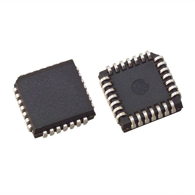
PLCC - 28 (Top View)
QP Package
*Notes: Unless otherwise indicated, voltages are referenced to
ground and currents are positive into, negative out of, the specified terminals, "Pulsed" is defined as a less than 10% duty cycle pulse with a maximum duration of 500µs.
THERMAL DATA
QP package: (see packaging section of UICC data book for more
details on thermal performance)
Thermal Resistance Junction to Leads, θjl . . . . . . . . 15°C/W
Thermal Resistance Junction to Ambient, θja . . . 30-40°C/W
Note: The above numbers for θjl are maximums for the limiting
thermal resistance of the package in a standard mounting configuration. The θja numbers are meant to be guidelines for the
thermal performance of the device/pc-board system. All of the
above numbers assume no ambient airflow.
PACKAGE PIN FUNCTION
FUNCTION
PIN
Inhibit
O/C Force
O/C Sense
Range
C/S(+)
Comp Adj
O/C Ind
AIN(+)
AIN(-)
VC(+) Supply
A Output
Pwr Gnd
Pwr Gnd
Pwr Gnd
Pwr Gnd
Pwr Gnd
Pwr Gnd
Pwr Gnd
B Output
VIN(+)
BIN(-)
BIN(+)
REF Input
C/S(-)
C/S Out
IDIF Out
IDIF REF
Ground
1
2
3
4
5
6
7
8
9
10
11
12
13
14
15
16
17
18
19
20
21
22
23
24
25
26
27
28
ELECTRICAL CHARACTERISTICS: Unless otherwise stated specifications hold for TA = 0°C to 70°C, VC(+) = VIN(+) =
12V, REF Input = VIN(+)/2, O/C Input & Inhibit Input = 0V.
PARAMETER
TEST CONDITIONS
MIN
TYP
MAX
UNITS
IOUT = OA
12
1.2
16
2.0
mA
mA
Supplies = 5V,IOUT = OA
12
16
mA
Supplies = 12V,IOUT = OA
13
18
mA
2.6
2.8
Input Supply
VIN (+)Supply Current
VC(+) Supply Current
Total Supply Current
VIN(+) UVLO Threshold
low to high
UVLO Threshold Hysterisis
V
300
mV
-.01
µA
Over-Current (O/C) Comparator
Input Bias Current
V input = 0.8V
-1.0
Thresholds
low to high
0.97
1.0
1.03
V
85
100
115
mV
0.2
0.45
V
5.0
µA
A Amplifier, VCM = 6V
4.0
mV
B Amplifier, VCM = 6V
12.0
mV
Threshold Hysterisis
O/C IND Vsat
IOUT = 5mA, V input low
O/C IND Leakage
VOUT = 20V
Power Amplifiers A and B
Input Offset Voltage
Input Bias Current
VCM = 6V
-500
-50
µΑ
CMRR
VCM = 0.5 to 13V, Supplies = 15V
70
90
dB
PSRR
VIN(+) = 4 to 15V, VCM = 1.5V
70
90
dB
Large Signal Voltage Gain
Supplies = 12V, VOUT = 1V, IOUT = 300mA
3.0
15.0
V/mV
to VOUT = 10.5V, IOUT = -300mA
2
�UC3178
Unless otherwise stated specifications hold for TA = 0°C to 70°C , VC(+) = VIN(+) = 12V,
ELECTRICAL
CHARACTERISTICS (cont.): REF Input = VIN(+)/2, O/C Input & Inhibit Input = 0V.
PARAMETER
TEST CONDITIONS
MIN
TYP
MAX
UNITS
Power Amplifiers A & B (cont.)
Gain Bandwith Product
A Amplifier
2.0
MHz
B Amplifier
1.0
MHz
Slew Rate
High-Side Current Limit
Output Saturation Voltage
High-Side Diode, Vf
0.45
1.0
V/µs
0.65
A
High-Side, IOUT = -100mA
0.75
V
High-Side, IOUT = -300mA
0.85
V
High-Side, IOUT = -450mA
0.9
V
Low-Side, IOUT = 100mA
0.2
V
Low-Side, IOUT = 300mA
0.25
V
Low-Side, IOUT = 450mA
0.30
V
Total Vsat, IOUT = 100mA
0.95
1.2
V
Total Vsat, IOUT = 300mA
1.05
1.4
V
Total Vsat, IOUT = 450mA
1.25
1.6
ID = 450mA
1.30
V
V
Current Sense Amplifier
Input Offset Voltage
VCM = 6V, Low range mode
2.0
mV
High range mode
4.0
mV
Input Offset Change
VCM = -1V to 13V, Supplies = 12V, Low Range Mode
2000
µV/V
with Common Mode Input
VCM = -1V to 13V, Supplies = 12V, High Range Mode
4000
µV/V
Voltage Gain
VDIFF = +1.0 to -1.0V, Vcm = 6V, High Range Mode
0.485
0.50
0.515
V/V
VDIFF = +1.0 to -1.0V, Vcm = 6V, Low Range Mode
1.95
2.0
2.05
V/V
0.1
0.1
0.3
0.3
V
V
27
µA/V
10
mV
Saturation Voltage
Low-Side, IOUT = 1mA
High-Side, IOUT = -1mA, Referenced to = VIN(+)
Input Bias Current at Ref. Input
(REF Input - C/S(+))/48kohms, Tj = 25°C
15
21
Sense Buffer CMRR
REF Input to IDIF REF, IOUT = ±1mA
IOUT = ±1mA, REF Input = 2V to 10V
70
90
IDIF REF to IDIF Out Current
IDIF = ± 100µA, IDIF Out = 1V
0.95
1.0
1.05
A/A
Ratio
IDIF = ±1mA, IDIF Out = 1V
IDIF Out = ± 1mA, VIN(+) = 4V to 15V,REF Input = 2V
IOUT = ±1mA, REF Input = 2V to10V, IDIF Out = 1V
0.94
1.0
1.06
A/A
1.0
5.0
µA/V
1.0
5.0
µA/V
0.6
1.1
1.7
V
-1.0
-0.5
0.6
1.1
1.7
V
50
100
µA
0.6
1.1
1.7
V
50
100
µA
0.02
0.1
V
Load Current Sense and Rectification
Sense Buffer Offset Voltage
IDIF Out Supply Sensitivity
IDIF Out Common Mode Sensitivity
(delta IDIF Out/delta REF Input)
dB
Auxiliary Functions
Inhibit Input Threshold
Inhibit Input Current
Inhibit Input = 1.7V
O/C Force Input Threshold
O/C Force Input Current
O/C Force Input = 1.7V
Range Input Threshold
Range Input Current
Range Input = 1.7V
COMP ADJ Pin Saturation
Range Input = 0V, Pin Current = ±500µA, Referenced
Voltage
to AOUT
COMP ADJ Leakage Current
Range Input = 1.7V, Supplies = 12V
AOUT-VComp Adj = ±6V
Total Supply Current When Inhibited
VIN(+) and VC(+) currents
Thermal Shutdown Temperature
1.0
165
3
µA
5.0
µA
1.5
mA
°C
�UC3178
PIN DESCRIPTIONS:
IDIF REF: Output of the IDIF sense buffer. Voltage on this
pin will track the applied voltage on the REF Input pin.
Current through this pin is full wave rectified and appears
as a current sourced from the IDIF OUT pin.
A & B OUT: Outputs for the A & B power amplifiers,
providing differential drive to the load during normal operation. During a UVLO, Inhibit, or O/C condition both of
these outputs will be in a high, source only state. Highside diodes are included to catch inductive load currents
flowing into these pins, inductive kicks on the low-side are
caught by the high-side output transistors.
Inhibit : A high impedance logic input that disables the A
and B power amplifiers, the IDIF sense buffer, and the
Current Sense amplifier. This input has an internal pull-up
AIN(+): Non-inverting input to the A amplifier. Normally tied that will inhibit the device if the input is left open.
to the REF Input when the current sense amplifier is used. O/C Force: Logic input that forces the O/C condition.
AIN(-): Inverting input to the A amplifier. Used as the sum- O/C IND: Open collector ouput that indicates, with an acming node to close the loop on the overall power tive low state, an O/C condition.
amplifier.
O/C Sense: Input to the Over Current Comparator. When
BIN(+): Non-inverting input to the B amplifier. This pin nor- this input is above its 1V threshold the low-side devices of
mally sets the reference point for the differential voltage both the A & B power amplifiers will be disabled forcing a
swing at the load.
high, source only, state at both outputs.
BIN(-): Inverting input to the B amplifier. Used to program PWR GND: Current return for all high level circuitry, this
the gain of the B amplifier.
pin should be connected to the same potential as GND.
COMP ADJ: The compensation adjust pin allows the user
to provide an auxiliary compensation network for the A amplifier that is only active when the current sense amplifier is
in the low range. With this option, the user can control the
change in bandwidth that would otherwise result from the
gain change in the feedback loop.
Range: When this pin is open or at a logic low potential,
the current sense amplifier will be in its low range mode.
In this mode the voltage gain of the amplifier will be 2. If
this pin is brought to a logic high, the gain of the current
sense amplifier will change into its high range value of
0.5. This factor of four change in gain will vary the overall
transconductance of the power amplifier by the same ratio, with the transconductance being the highest in the
high mode. This feature allows improved dynamic range
of load current control for a given control input range and
resolution.
C/S(+): The non-inverting input to the current sense amplifier is typically tied to the load side of the series current
sense resistor. This pin can be pulled below ground during
an abrupt load current change with an inductive load.
Proper operation of the current sense amplifier will result if
this pin does not go below ground by an amount greater REF Input: Sets the Reference level at the C/S Output,
than:
and is normally tied to the system reference level for in(REF Input / 2 ) - 0.3V.
puts to the power amplifier.
C/S(-): The inverting input to the current sense amplifier is V
IN(+): Provides bias supply to the device. The High-Side
typically tied to the connection between the B amplifier drive to the power stages on both the A and B amplifiers
output and the current sense resistor that is in series with is referenced to this pin. The High-side saturation voltthe load.
ages, and UVLO are specified and measured with respect
C/S Output: The output of the current sense amplifier has to this supply pin.
a 1.5mA current source pull-up and an active NPN pull- V
C(+): This supply pin is the high current supply to the
down. The output will pull to within 0.3V of either rail with
collectors of the high-side NPN output devices on the A
a load current of less than 1mA.
and B amplifiers. This supply should be powered whenGND: Reference point for the internal reference, O/C ever the A or B amplifiers are to be activated. This pin can
comparator, and other low-level circuitry.
operate approximately 400mV below the VIN(+) supply
IDIF OUT: Current source output pin. The value of the out- without affecting the voltage available to the load.
put current is nominally equal to the magnitude of the
current through the IDIF REF pin.
4
�UC3178
TYPICAL APPLICATION
UDG-92009
Power amplifier transconductance
1
Il RB
Go =
=
•
Vs RA AV CS • RS
where:
Il is the load current
Vs is the input command voltage
AVCS is the current sense amplifier gain
= 2.0 in low range mode
= 0.5 in high range mode
VO/C is the 1.0V over-current comparator threshold
Peak commanded load current
RD
IlMAX = Vo/c •
RS • AVCS • RE
UNITRODE INTEGRATED CIRCUITS
7 CONTINENTAL BLVD.• MERRIMACK, NH 03054
TEL (603) 424-2410 • FAX (603) 424-3460
5
�PACKAGE OPTION ADDENDUM
www.ti.com
30-Jul-2011
PACKAGING INFORMATION
Orderable Device
UC3178QP
Status
(1)
ACTIVE
Package Type Package
Drawing
PLCC
FN
Pins
Package Qty
28
37
Eco Plan
(2)
Green (RoHS
& no Sb/Br)
Lead/
Ball Finish
MSL Peak Temp
(3)
Samples
(Requires Login)
CU NIPDAU Level-3-260C-168 HR
(1)
The marketing status values are defined as follows:
ACTIVE: Product device recommended for new designs.
LIFEBUY: TI has announced that the device will be discontinued, and a lifetime-buy period is in effect.
NRND: Not recommended for new designs. Device is in production to support existing customers, but TI does not recommend using this part in a new design.
PREVIEW: Device has been announced but is not in production. Samples may or may not be available.
OBSOLETE: TI has discontinued the production of the device.
(2)
Eco Plan - The planned eco-friendly classification: Pb-Free (RoHS), Pb-Free (RoHS Exempt), or Green (RoHS & no Sb/Br) - please check http://www.ti.com/productcontent for the latest availability
information and additional product content details.
TBD: The Pb-Free/Green conversion plan has not been defined.
Pb-Free (RoHS): TI's terms "Lead-Free" or "Pb-Free" mean semiconductor products that are compatible with the current RoHS requirements for all 6 substances, including the requirement that
lead not exceed 0.1% by weight in homogeneous materials. Where designed to be soldered at high temperatures, TI Pb-Free products are suitable for use in specified lead-free processes.
Pb-Free (RoHS Exempt): This component has a RoHS exemption for either 1) lead-based flip-chip solder bumps used between the die and package, or 2) lead-based die adhesive used between
the die and leadframe. The component is otherwise considered Pb-Free (RoHS compatible) as defined above.
Green (RoHS & no Sb/Br): TI defines "Green" to mean Pb-Free (RoHS compatible), and free of Bromine (Br) and Antimony (Sb) based flame retardants (Br or Sb do not exceed 0.1% by weight
in homogeneous material)
(3)
MSL, Peak Temp. -- The Moisture Sensitivity Level rating according to the JEDEC industry standard classifications, and peak solder temperature.
Important Information and Disclaimer:The information provided on this page represents TI's knowledge and belief as of the date that it is provided. TI bases its knowledge and belief on information
provided by third parties, and makes no representation or warranty as to the accuracy of such information. Efforts are underway to better integrate information from third parties. TI has taken and
continues to take reasonable steps to provide representative and accurate information but may not have conducted destructive testing or chemical analysis on incoming materials and chemicals.
TI and TI suppliers consider certain information to be proprietary, and thus CAS numbers and other limited information may not be available for release.
In no event shall TI's liability arising out of such information exceed the total purchase price of the TI part(s) at issue in this document sold by TI to Customer on an annual basis.
Addendum-Page 1
�MECHANICAL DATA
MPLC004A – OCTOBER 1994
FN (S-PQCC-J**)
PLASTIC J-LEADED CHIP CARRIER
20 PIN SHOWN
Seating Plane
0.004 (0,10)
0.180 (4,57) MAX
0.120 (3,05)
0.090 (2,29)
D
D1
0.020 (0,51) MIN
3
1
19
0.032 (0,81)
0.026 (0,66)
4
E
18
D2 / E2
E1
D2 / E2
8
14
0.021 (0,53)
0.013 (0,33)
0.007 (0,18) M
0.050 (1,27)
9
13
0.008 (0,20) NOM
D/E
D2 / E2
D1 / E1
NO. OF
PINS
**
MIN
MAX
MIN
MAX
MIN
MAX
20
0.385 (9,78)
0.395 (10,03)
0.350 (8,89)
0.356 (9,04)
0.141 (3,58)
0.169 (4,29)
28
0.485 (12,32)
0.495 (12,57)
0.450 (11,43)
0.456 (11,58)
0.191 (4,85)
0.219 (5,56)
44
0.685 (17,40)
0.695 (17,65)
0.650 (16,51)
0.656 (16,66)
0.291 (7,39)
0.319 (8,10)
52
0.785 (19,94)
0.795 (20,19)
0.750 (19,05)
0.756 (19,20)
0.341 (8,66)
0.369 (9,37)
68
0.985 (25,02)
0.995 (25,27)
0.950 (24,13)
0.958 (24,33)
0.441 (11,20)
0.469 (11,91)
84
1.185 (30,10)
1.195 (30,35)
1.150 (29,21)
1.158 (29,41)
0.541 (13,74)
0.569 (14,45)
4040005 / B 03/95
NOTES: A. All linear dimensions are in inches (millimeters).
B. This drawing is subject to change without notice.
C. Falls within JEDEC MS-018
POST OFFICE BOX 655303
• DALLAS, TEXAS 75265
1
�IMPORTANT NOTICE
Texas Instruments Incorporated and its subsidiaries (TI) reserve the right to make corrections, modifications, enhancements, improvements,
and other changes to its products and services at any time and to discontinue any product or service without notice. Customers should
obtain the latest relevant information before placing orders and should verify that such information is current and complete. All products are
sold subject to TI’s terms and conditions of sale supplied at the time of order acknowledgment.
TI warrants performance of its hardware products to the specifications applicable at the time of sale in accordance with TI’s standard
warranty. Testing and other quality control techniques are used to the extent TI deems necessary to support this warranty. Except where
mandated by government requirements, testing of all parameters of each product is not necessarily performed.
TI assumes no liability for applications assistance or customer product design. Customers are responsible for their products and
applications using TI components. To minimize the risks associated with customer products and applications, customers should provide
adequate design and operating safeguards.
TI does not warrant or represent that any license, either express or implied, is granted under any TI patent right, copyright, mask work right,
or other TI intellectual property right relating to any combination, machine, or process in which TI products or services are used. Information
published by TI regarding third-party products or services does not constitute a license from TI to use such products or services or a
warranty or endorsement thereof. Use of such information may require a license from a third party under the patents or other intellectual
property of the third party, or a license from TI under the patents or other intellectual property of TI.
Reproduction of TI information in TI data books or data sheets is permissible only if reproduction is without alteration and is accompanied
by all associated warranties, conditions, limitations, and notices. Reproduction of this information with alteration is an unfair and deceptive
business practice. TI is not responsible or liable for such altered documentation. Information of third parties may be subject to additional
restrictions.
Resale of TI products or services with statements different from or beyond the parameters stated by TI for that product or service voids all
express and any implied warranties for the associated TI product or service and is an unfair and deceptive business practice. TI is not
responsible or liable for any such statements.
TI products are not authorized for use in safety-critical applications (such as life support) where a failure of the TI product would reasonably
be expected to cause severe personal injury or death, unless officers of the parties have executed an agreement specifically governing
such use. Buyers represent that they have all necessary expertise in the safety and regulatory ramifications of their applications, and
acknowledge and agree that they are solely responsible for all legal, regulatory and safety-related requirements concerning their products
and any use of TI products in such safety-critical applications, notwithstanding any applications-related information or support that may be
provided by TI. Further, Buyers must fully indemnify TI and its representatives against any damages arising out of the use of TI products in
such safety-critical applications.
TI products are neither designed nor intended for use in military/aerospace applications or environments unless the TI products are
specifically designated by TI as military-grade or "enhanced plastic." Only products designated by TI as military-grade meet military
specifications. Buyers acknowledge and agree that any such use of TI products which TI has not designated as military-grade is solely at
the Buyer's risk, and that they are solely responsible for compliance with all legal and regulatory requirements in connection with such use.
TI products are neither designed nor intended for use in automotive applications or environments unless the specific TI products are
designated by TI as compliant with ISO/TS 16949 requirements. Buyers acknowledge and agree that, if they use any non-designated
products in automotive applications, TI will not be responsible for any failure to meet such requirements.
Following are URLs where you can obtain information on other Texas Instruments products and application solutions:
Products
Applications
Audio
www.ti.com/audio
Communications and Telecom www.ti.com/communications
Amplifiers
amplifier.ti.com
Computers and Peripherals
www.ti.com/computers
Data Converters
dataconverter.ti.com
Consumer Electronics
www.ti.com/consumer-apps
DLP® Products
www.dlp.com
Energy and Lighting
www.ti.com/energy
DSP
dsp.ti.com
Industrial
www.ti.com/industrial
Clocks and Timers
www.ti.com/clocks
Medical
www.ti.com/medical
Interface
interface.ti.com
Security
www.ti.com/security
Logic
logic.ti.com
Space, Avionics and Defense
www.ti.com/space-avionics-defense
Power Mgmt
power.ti.com
Transportation and
Automotive
www.ti.com/automotive
Microcontrollers
microcontroller.ti.com
Video and Imaging
www.ti.com/video
RFID
www.ti-rfid.com
Wireless
www.ti.com/wireless-apps
RF/IF and ZigBee® Solutions
www.ti.com/lprf
TI E2E Community Home Page
e2e.ti.com
Mailing Address: Texas Instruments, Post Office Box 655303, Dallas, Texas 75265
Copyright © 2011, Texas Instruments Incorporated
�


 工商网监
湘ICP备2023018690号
工商网监
湘ICP备2023018690号
