Order
Now
Product
Folder
Support &
Community
Tools &
Software
Technical
Documents
UCC27611
SLUSBA5F – DECEMBER 2012 – REVISED MARCH 2018
UCC27611 5-V, 4-A to 6-A Low Side GaN Driver
1 Features
3 Description
•
The UCC27611 is a single-channel, high-speed, gate
driver optimized for 5-V drive, specifically addressing
enhancement mode GaN FETs. The drive voltage
VREF is precisely controlled by internal linear
regulator to 5 V. The UCC27611 offers asymmetrical
rail-to-rail peak current drive capability with 4-A
source and 6-A sink. Split output configuration allows
individual turnon and turnoff time optimization
depending on FET. Package and pinout with
minimum parasitic inductances reduce the rise and
fall time and limit the ringing. Additionally, the short
propagation delay with minimized tolerances and
variations allows efficient operation at high
frequencies. The 1-Ω and 0.35-Ω resistance boosts
immunity to hard switching with high slew rate dV and
dt.
1
•
•
•
•
•
•
•
•
•
•
•
•
•
•
Enhancement Mode Gallium Nitride FETs
(eGANFETs)
4-V to 18-V Single Supply Range VDD Range
Drive Voltage VREF Regulated to 5 V
4-A Peak Source and 6-A Peak Sink Drive
Current
1-Ω and 0.35-Ω Pullup and Pulldown Resistance
(Maximize High Slew-Rate dV and dt Immunity)
Split Output Configuration (Allows Turnon and
Turnoff Optimization for Individual FETs)
Fast Propagation Delays (14-ns Typical)
Fast Rise and Fall Times (9-ns and 5-ns Typical)
TTL and CMOS Compatible Inputs (Independent
of Supply Voltage Allow Easy Interface-to-Digital
and Analog Controllers)
Dual-Input Design Offering Drive Flexibility (Both
Inverting and Noninverting Configurations)
Output Held Low When Inputs Are Floating
VDD Under Voltage Lockout (UVLO)
Optimized Pinout Compatible With eGANFET
Footprint for Easy Layout
2.00 mm × 2.00 mm SON-6 Package With
Exposed Thermal and Ground Pad, (Minimized
Parasitic Inductances to Reduce Gate Ringing)
Operating Temperature Range of –40°C to 140°C
Device Information(1)
2 Applications
•
•
•
•
•
The independence from VDD input signal thresholds
ensure TTL and CMOS low-voltage logic
compatibility. For safety reason, when the input pins
are in a floating condition, the internal input pullup
and pulldown resistors hold the output LOW. Internal
circuitry on VREF pin provides an undervoltage
lockout function that holds output LOW until VREF
supply voltage is within operating range. UCC27611
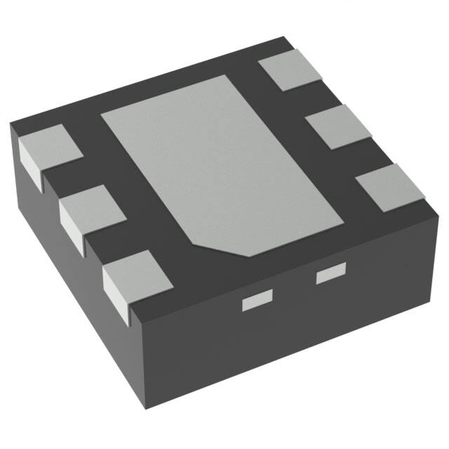
is offered in a small 2.00 mm × 2.00 mm SON-6
package (DRV) with exposed thermal and ground pad
that improves the package power-handling capability.
The UCC27611 operates over wide temperature
range from –40°C to 140°C.
PART NUMBER
Switch-Mode Power Supplies
DC-to-DC Converters
Synchronous Rectification
Solar Inverters, Motor Control, UPS
Envelope Tracking Power Supplies
PACKAGE
UCC27611
BODY SIZE (NOM)
SON (6)
2.00 mm × 2.00 mm
(1) For all available packages, see the orderable addendum at
the end of the datasheet.
Typical Application Diagram
Non-Inverting Input
4.5 V to 18 V
VREF
Inverting Input
4.5 V to 18 V
VSOURCE
VDD
VREF
VDD
C3
C2
VSOURCE
C3
C2
L1
L1
UCC27611
UCC27611
D1
1
VDD
VREF
D1
6
VOUT
1
VDD
VREF
6
VOUT
Q1
Q1
R1
2
IN-
OUTH
R1
5
IN-
2
IN-
OUTH
5
VREF
3
IN+
OUTL
4
+
R2
IN+
3
IN+
OUTL
4
+
R2
C1
GND
GND
7
7
C1
1
An IMPORTANT NOTICE at the end of this data sheet addresses availability, warranty, changes, use in safety-critical applications,
intellectual property matters and other important disclaimers. PRODUCTION DATA.
�UCC27611
SLUSBA5F – DECEMBER 2012 – REVISED MARCH 2018
www.ti.com
Table of Contents
1
2
3
4
5
6
7
Features ..................................................................
Applications ...........................................................
Description .............................................................
Revision History.....................................................
Pin Configuration and Functions .........................
Specifications.........................................................
1
1
1
2
3
3
6.1
6.2
6.3
6.4
6.5
6.6
6.7
3
4
4
4
5
5
7
Absolute Maximum Ratings ......................................
ESD Ratings..............................................................
Recommended Operating Conditions.......................
Thermal Information ..................................................
Electrical Characteristics...........................................
Switching Characteristics ..........................................
Typical Characteristics ..............................................
Detailed Description .............................................. 8
7.1 Overview ................................................................... 8
7.2 Functional Block Diagram ......................................... 8
7.3 Feature Description................................................... 8
7.4 Device Functional Modes........................................ 11
8
Application and Implementation ........................ 12
8.1 Application Information............................................ 12
8.2 Typical Application ................................................. 13
9 Power Supply Recommendations...................... 18
10 Layout................................................................... 20
10.1 Layout Guidelines ................................................. 20
10.2 Layout Example .................................................... 20
11 Device and Documentation Support ................. 21
11.1
11.2
11.3
11.4
11.5
11.6
Documentation Support ........................................
Receiving Notification of Documentation Updates
Community Resources..........................................
Trademarks ...........................................................
Electrostatic Discharge Caution ............................
Glossary ................................................................
21
21
21
21
21
21
12 Mechanical, Packaging, and Orderable
Information ........................................................... 21
4 Revision History
NOTE: Page numbers for previous revisions may differ from page numbers in the current version.
Changes from Revision E (February 2018) to Revision F
Page
•
Changed Power Up (Noninverting Drive) graphic ................................................................................................................. 9
•
Changed Power Up (Inverting Drive) graphic......................................................................................................................... 9
Changes from Revision D (October 2017) to Revision E
•
Changed title ......................................................................................................................................................................... 1
Changes from Revision C (December 2015) to Revision D
•
2
Page
Added ESD Ratings table, Feature Description section, Device Functional Modes, Application and Implementation
section, Power Supply Recommendations section, Layout section, Device and Documentation Support section, and
Mechanical, Packaging, and Orderable Information section .................................................................................................. 1
Changes from Revision A (December 2012) to Revision B
•
Page
Changed title ......................................................................................................................................................................... 1
Changes from Revision B (May 2013) to Revision C
•
Page
Page
Added Electrical Characteristics Inputs (IN+, IN–) section values ......................................................................................... 5
Submit Documentation Feedback
Copyright © 2012–2018, Texas Instruments Incorporated
Product Folder Links: UCC27611
�UCC27611
www.ti.com
SLUSBA5F – DECEMBER 2012 – REVISED MARCH 2018
5 Pin Configuration and Functions
DRV Package
6-Pin SON With Exposed Thermal Pad
Top View
VDD
1
IN-
2
IN+
3
GND PAD
Pin 7
6
VREF
5
OUTH
4
OUTL
Pin Functions
PIN
NO.
NAME
I/O
DESCRIPTION
1
VDD
I
Bias supply input. Connect a ceramic capacitor minimum from this pin to the GND pin as
close as possible to the device with the shortest trace lengths possible.
2
IN–
I
Inverting input. Pull IN+ to VDD to enable output, when using the driver device in Inverting
configuration.
3
IN+
I
Noninverting input. Pull IN– to GND to enable output, when using the driver device in
noninverting configuration.
4
OUTL
O
6-A sink current output of driver.
5
OUTH
O
4-A source current output of driver.
6
VREF
O
Drive voltage, output of internal linear regulator. Connect a ceramic capacitor minimum from
this pin to the GND pin as close as possible to the device with the shortest trace lengths
possible.
7
GND PAD
—
Ground. All signals are referenced to this node.
6 Specifications
6.1 Absolute Maximum Ratings
over operating free-air temperature range (unless otherwise noted) (1)
MIN
MAX
UNIT
Supply voltage
–0.3
20
V
OUTH
–0.3
VREF + 0.3
V
OUTL
–0.3
VREF + 0.3
V
6
V
IN+, IN–
–0.3
20
V
Iout_DC
Continuous source current of OUTH/sink current of OUTL
0.3
0.6
A
Iout_pulsed
Continuous source current of OUTH/sink current of OUTL
(0.5 µs),
4
6
A
Lead temperature, soldering, 10 sec.
300
°C
Lead temperature, reflow
260
°C
VDD
VREF
TJ
Operating virtual junction temperature
–40
150
°C
Tstg
Storage temperature
–65
150
°C
(1)
Stresses beyond those listed under Absolute Maximum Ratings may cause permanent damage to the device. These are stress ratings
only, which do not imply functional operation of the device at these or any other conditions beyond those indicated under Recommended
Operating Conditions. Exposure to absolute-maximum-rated conditions for extended periods may affect device reliability.
Submit Documentation Feedback
Copyright © 2012–2018, Texas Instruments Incorporated
Product Folder Links: UCC27611
3
�UCC27611
SLUSBA5F – DECEMBER 2012 – REVISED MARCH 2018
www.ti.com
6.2 ESD Ratings
VALUE
V(ESD)
(1)
(2)
Electrostatic discharge
Human-body model (HBM), per ANSI/ESDA/JEDEC JS-001 (1)
±2000
Charged-device model (CDM), per JEDEC specification JESD22C101 (2)
±500
UNIT
V
JEDEC document JEP155 states that 500-V HBM allows safe manufacturing with a standard ESD control process.
JEDEC document JEP157 states that 250-V CDM allows safe manufacturing with a standard ESD control process.
6.3 Recommended Operating Conditions
over operating free-air temperature range (unless otherwise noted)
MIN
NOM
MAX
12
18
VDD
Supply voltage
4
IN
Input voltage
0
IN+, IN– resistance
TJ
Operating junction temperature
–40
UNIT
V
18
V
100
kΩ
140
°C
6.4 Thermal Information
UCC27611
THERMAL METRIC (1)
DRV (SON)
UNIT
6 PINS
RθJA
Junction-to-ambient thermal resistance
80.3
°C/W
RθJC(top)
Junction-to-case (top) thermal resistance
11.9
°C/W
RθJB
Junction-to-board thermal resistance
49.7
°C/W
ψJT
Junction-to-top characterization parameter
5.5
°C/W
ψJB
Junction-to-board characterization parameter
50.1
°C/W
RθJC(bot)
Junction-to-case (bottom) thermal resistance
18.8
°C/W
(1)
4
For more information about traditional and new thermal metrics, see the Semiconductor and IC Package Thermal Metrics application
report.
Submit Documentation Feedback
Copyright © 2012–2018, Texas Instruments Incorporated
Product Folder Links: UCC27611
�UCC27611
www.ti.com
SLUSBA5F – DECEMBER 2012 – REVISED MARCH 2018
6.5 Electrical Characteristics
VDD = 12 V, TA = TJ = –40 °C to 140 °C, 2-µF capacitor from VDD to GND and from VREF to GND. Currents are positive
into, negative out of the specified terminal. OUTH and OUTL are tied together. (unless otherwise noted) (1)
PARAMETER
TEST CONDITIONS
MIN
TYP
MAX
UNIT
100
180
75
160
3.55
3.8
4.15
V
3.3
3.55
3.9
V
BIAS CURRENT
IDD(off)
VDD = 3, IN+ = VDD,
IN– = GND
Start-up current
IN+ = GND, IN– = VDD
μA
UNDER VOLTAGE LOCKOUT (UVLO)
VDD(on)
Supply start threshold
VDD(off)
Minimum operating voltage after supply
start
VDD_H
Supply voltage hysteresis
0.25
V
INPUTS (IN+, IN–)
VIN_L
Input signal low threshold
Output high for IN– pin,
Output Low for IN+ pin
0.9
1.1
1.3
V
VIN_H
Input signal high threshold
Output high for IN+ pin,
Output low for IN– pin
1.85
2.05
2.25
V
VIN_HYS
Input signal hysteresis
0.7
0.95
1.2
V
4.75
5
VREF
VREF
VREF regulator output
5.15
V
VREF_line
VREF line regulation
VDD from 6 V to 18 V
0.05
V
VREF_load
VREF load regulation
IR from 0 mA to 50 mA
0.075
V
ISCC
Short circuit current
–90
–75
–60
mA
OUTPUTS (OUTH/OUTL AND OUT)
ISRC/SNK
Source peak current (OUTH) / sink peak
current (OUTL) (2)
CLOAD = 0.22 µF, FSW = 1 kHz,
VOH
OUTH high voltage
IOUTH = –10 mA
VOL
OUTL low voltage
IOUTL = 10 mA
ROH
ROL
(1)
(2)
OUTH pullup resistance
OUTH pulldown resistance
(2)
–4/+6
A
VDD
–0.05
V
0.02
TA = 25 °C,
IOUT = –25 mA to –50 mA
V
1
Ω
TA = –40 °C to 140 °C,
IOUT = –50 mA
2
TA = 25 °C,
IOUT = 25 mA to 50 mA
0.35
Ω
TA = –40°C to 140°C,
IOUT = 50 mA
1.5
Device operational with output switching.
Ensured by design, not tested in production.
6.6 Switching Characteristics
over operating free-air temperature range (unless otherwise noted)
PARAMETER
TEST CONDITIONS
MIN
TYP
MAX
UNIT
tR
Rise time (1)
CLOAD = 1 nF
5
ns
tF
Fall time (1)
CLOAD = 1 nF
5
ns
tD1
Turnon propagation delay
(1)
CLOAD = 1 nF, IN = 0 V to 5 V
14
25
ns
tD2
Turnoff propagation delay (1)
CLOAD = 1 nF, IN = 5 V to 0 V
14
25
ns
(1)
See Figure 1 and Figure 2 timing diagrams.
Submit Documentation Feedback
Copyright © 2012–2018, Texas Instruments Incorporated
Product Folder Links: UCC27611
5
�UCC27611
SLUSBA5F – DECEMBER 2012 – REVISED MARCH 2018
www.ti.com
High
Input (IN+)
Low
High
Input (IN–)
Low
90%
Output
10%
tD1 tR
tD2 tF
Figure 1. Noninverting Configuration
(OUTH and OUTL Are Tied Together)
High
Input (IN+)
Low
High
Input (IN–)
Low
90%
Output
10%
tD1 tF
tD2 tR
Figure 2. Inverting Configuration
(OUTH and OUTL Are Tied Together)
6
Submit Documentation Feedback
Copyright © 2012–2018, Texas Instruments Incorporated
Product Folder Links: UCC27611
�UCC27611
www.ti.com
SLUSBA5F – DECEMBER 2012 – REVISED MARCH 2018
6.7 Typical Characteristics
18
IN+ Propagation Delay (ns)
VREF (V)
5
4.9
Turn−On
Turn−Off
16
14
12
10
VDD = 12 V
4.8
−50
0
50
Temperature (°C)
100
8
−50
150
0
G001
Figure 3. Reference Voltage vs Temperature
100
150
G001
Figure 4. IN+ Propagation Delay
0.4
20
Turn−On
Turn−Off
UVLO Hysterisis
18
UVLO Hystersis (V)
IN− Propagation Delay (ns)
50
Temperature (°C)
16
14
0.3
12
VDD = 12 V
10
−50
0
50
Temperature (°C)
100
0.2
−50
150
0
G001
Figure 5. IN– Propagation Delay
150
G001
6
VDD = 12 V
CLoad = 1.8nF
VDD = 12 V
CLoad = 1.8nF
5.8
Fall Time (ns)
5.8
Rise Time (ns)
100
Figure 6. UVLO Hysteresis
6
5.6
5.4
5.2
5
−50
50
Temperature (°C)
5.6
5.4
5.2
0
50
Temperature (°C)
100
150
5
−50
G001
Figure 7. Rise Time
0
50
Temperature (°C)
100
150
G001
Figure 8. Fall Time
Submit Documentation Feedback
Copyright © 2012–2018, Texas Instruments Incorporated
Product Folder Links: UCC27611
7
�UCC27611
SLUSBA5F – DECEMBER 2012 – REVISED MARCH 2018
www.ti.com
7 Detailed Description
7.1 Overview
The UCC27611 is a single-channel, high-speed, gate driver capable of effectively driving MOSFET power
switches (specifically addressing enhancement mode GaN FETs) by up to 4-A source and 6-A sink peak current.
Strong sink capability in asymmetrical drive boosts immunity against parasitic Miller turnon effect. The drive
voltage VREF is precisely regulated by internal linear regulator to 5 V, which is optimized for driving
enhancement mode GaN FET. The input threshold of UCC27611 is based on TTL and CMOS compatible lowvoltage logic, which is fixed and independent of VDD supply voltage. The 0.95-V typical hysteresis offers
excellent noise immunity. For safety reason, when the input pins are in a floating condition, the internal input
pullup and pulldown resistors hold the output LOW. The device also features a split-output configuration, where
the gate-drive current is sourced through the OUTH pin and sunk through the OUTL pin. This pin arrangement
allows the user to apply independent turnon and turnoff resistors to the OUTH and OUTL pins, respectively, and
easily control the switching slew rates. The driver has rail-to-rail drive capability and extremely small propagation
delay, with minimized tolerances and variations. Package and pinout with minimum parasitic inductances reduce
the rise and fall time, and limit the ringing allows efficient operation at high frequencies.
7.2 Functional Block Diagram
IN+
VREF
3
VDD
IN-
2
VDD
VDD
1
VREF
VREF
LDO
UVLO
6
VREF
5
OUTH
4
OUTL
7
GND
7.3 Feature Description
7.3.1 VDD and Undervoltage Lockout
The UCC27611 device has internal Under Voltage LockOut (UVLO) protection feature on the VDD pin supply
circuit blocks. Whenever the driver is in UVLO condition (that is when VDD voltage less than VDD(on) during power
up, and when VDD voltage is less than VDD(off) during power down), this circuit holds all outputs LOW, regardless
of the status of the inputs. The UVLO is typically 3.8 V, with 250-mV typical hysteresis. This hysteresis helps
prevent chatter when low VDD supply voltages have noise from the power supply, and also when there are
droops in the VDD bias voltage when the system commences switching and there is a sudden increase in IDD.
The capability to operate at low-voltage levels such as below 5 V, along with best-in-class switching
characteristics, is especially suited for driving emerging GaN wide bandgap power semiconductor devices.
For example, at power up, the UCC27611 driver output remains LOW until the VDD voltage reaches the UVLO
threshold. The magnitude of the OUT signal rises with VDD, until steady-state VDD is reached. In the
noninverting operation (PWM signal applied to IN+ pin), see Figure 9, the output remains LOW until the UVLO
threshold is reached, and then the output is in-phase with the input. In the inverting operation (PWM signal
applied to IN– pin), see Figure 10, the output remains LOW until the UVLO threshold is reached, and then the
output is out-phase with the input. In both cases, the unused input pin must be properly biased to enable the
output.
8
Submit Documentation Feedback
Copyright © 2012–2018, Texas Instruments Incorporated
Product Folder Links: UCC27611
�UCC27611
www.ti.com
SLUSBA5F – DECEMBER 2012 – REVISED MARCH 2018
Feature Description (continued)
NOTE
The output turns to high state only if IN+ pin is high and IN– pin is low after the UVLO
threshold is reached.
4.5 V to 18 V
VREF
VSOURCE
VDD
C3
C2
L1
UCC27611
1
VDD
VREF
D1
6
VOUT
Q1
R1
2
IN-
OUTH
5
3
IN+
OUTL
4
+
R2
IN+
C1
GND
7
Figure 9. Power Up (Noninverting Drive)
4.5 V to 18 V
VREF
VSOURCE
VDD
C3
C2
L1
UCC27611
D1
1
VDD
VREF
6
VOUT
R1
IN-
2
IN-
OUTH
Q1
5
R2
VREF
3
IN+
OUTL
+
C1
4
GND
7
Figure 10. Power Up (Inverting Drive)
7.3.2 Operating Supply Current
The UCC27611 device features very low quiescent IDD current. The total supply current is the sum of the
quiescent IDD current, the average IOUT current due to switching, and finally any current related to pullup
resistors on the unused input pin. For example, when the inverting input pin is pulled low, additional current is
drawn from VDD supply through the pullup resistors (see Functional Block Diagram). Knowing the operating
frequency (fSW) and the MOSFET gate (QG) charge at the drive voltage being used, the average IOUT current can
be calculated as product of QG and fSW.
Submit Documentation Feedback
Copyright © 2012–2018, Texas Instruments Incorporated
Product Folder Links: UCC27611
9
�UCC27611
SLUSBA5F – DECEMBER 2012 – REVISED MARCH 2018
www.ti.com
Feature Description (continued)
7.3.3 Input Stage
The input pins of the UCC27611 device is based on a TTL and CMOS compatible input threshold logic that is
independent of the VDD supply voltage. With typical high threshold = 2.05 V and typical low threshold = 1.1 V,
the logic level thresholds can be conveniently driven with PWM control signals derived from 3.3-V and 5-V digital
power controllers. Wider hysteresis (typical 1 V) offers enhanced noise immunity compared to traditional TTL
logic implementations, where the hysteresis is typically less than 0.5 V. These devices also feature tight control
of the input pin threshold voltage levels, which eases system design considerations, and ensures stable
operation across temperature. The very low input capacitance on these pins reduces loading, and increases
switching speed.
The device features an important safety function wherein, whenever any of the input pins are in a floating
condition, the output of the respective channel is held in the low state. This is achieved using VDD pullup
resistors on all the inverting inputs (IN– pin), or GND pulldown resistors on all the noninverting input pins (IN+
pin)(see Functional Block Diagram).
The device also features a dual input configuration, with two input pins available to control the state of the output.
The user has the flexibility to drive the device using either a noninverting input pin (IN+), or an inverting input pin
(IN–). The state of the output pin is dependent on the bias of both the IN+ and IN– pins. See Table 1 input and
output logic truth table, and the Figure 12 for additional clarification.
7.3.4 Enable Function
An enable and disable function can be easily implemented in the UCC27611 device using the unused input pin.
When IN+ is pulled down to GND, or IN– is pulled down to VDD, the output is disabled. Thus, IN+ pin can be
used like an enable pin that is based on active high logic, while IN– can be used like an enable pin that is based
on active low logic.
7.3.5 Output Stage
The output stage of the UCC27611 device is illustrated in Figure 11. OUTH and OUTL are externally connected
and pinned out as OUTH and OUTL pins. The UCC27611 device features a unique architecture on the output
stage, which delivers the highest peak source current when it is most needed during the Miller plateau region of
the power switch turnon transition (when the power switch drain and collector voltage experiences dV and dt).
The device output stage features a hybrid pullup structure using a parallel arrangement of N-channel and Pchannel MOSFET devices. By turning on the N-channel MOSFET, during a narrow instant when the output
changes state from low to high, the gate-driver device is able to deliver a brief boost in the peak-sourcing current,
enabling fast turnon.
VREF
R OH
R NMOS, Pull Up
Input Signal Anti Shoot Through
Circuitry
Gate
Voltage
Boost
OUTH
OUTL
Narrow Pulse at
each Turn On
R OL
Figure 11. UCC27611 Device Gate Driver Output Structure
10
Submit Documentation Feedback
Copyright © 2012–2018, Texas Instruments Incorporated
Product Folder Links: UCC27611
�UCC27611
www.ti.com
SLUSBA5F – DECEMBER 2012 – REVISED MARCH 2018
Feature Description (continued)
The ROH parameter (see Electrical Characteristics) is a DC measurement, and it is representative of the onresistance of the P-channel device only, because the N-channel device is turned on only during output change of
state from low to high. Thus, the effective resistance of the hybrid pullup stage is much lower than what is
represented by ROH parameter. The pulldown structure is composed of a N-channel MOSFET only. The ROL
parameter (see Electrical Characteristics), which is also a DC measurement, is representative of true impedance
of the pulldown stage in the device.
The driver output voltage swings between VDD and GND, providing rail-to-rail operation thanks to the MOS
output stage that delivers very low dropout. The presence of the MOSFET body diodes also offers low
impedance to switching overshoots and undershoots. This means that in many cases, external Schottky diode
clamps may be eliminated. The outputs of these drivers are designed to withstand 500-mA reverse current
without either damage to the device, or logic malfunction.
7.3.6 Low Propagation Delays
The UCC27611 driver device feature best-in-class input-to-output propagation delay of 14 ns (typical) at VDD =
12 V. This promises the lowest level of pulse transmission distortion available from industry standard gate-driver
devices for high-frequency switching applications. There is very little variation of the propagation delay with
temperature and supply voltage as well, offering typically less than 20-ns propagation delays across the entire
range of application conditions.
7.4 Device Functional Modes
Table 1 shows the input and output logic.
Table 1. Truth Table
IN– PIN
OUTH PIN
OUTL PIN
OUT (OUTH and OUTL
pins tied together)
L
L
High-impedance
L
L
L
H
High-impedance
L
L
H
L
H
High-impedance
H
H
H
High-impedance
L
L
IN+ PIN
Submit Documentation Feedback
Copyright © 2012–2018, Texas Instruments Incorporated
Product Folder Links: UCC27611
11
�UCC27611
SLUSBA5F – DECEMBER 2012 – REVISED MARCH 2018
www.ti.com
8 Application and Implementation
NOTE
Information in the following applications sections is not part of the TI component
specification, and TI does not warrant its accuracy or completeness. TI’s customers are
responsible for determining suitability of components for their purposes. Customers must
validate and test their design implementation to confirm system functionality.
8.1 Application Information
High-current gate-driver devices are required in switching power applications for a variety of reasons. To effect
the fast switching of power devices, and reduce associated switching-power losses, a powerful gate-driver device
employs between the PWM output of control devices and the gates of the power semiconductor devices. Further,
gate-driver devices are indispensable when it is not feasible for the PWM controller device to directly drive the
gates of the switching devices. With the advent of digital power, this situation is often encountered because the
PWM signal from the digital controller is often a 3.3-V logic signal that is not capable of effectively turning on a
power switch. A level-shifting circuitry is required to boost the 3.3-V signal to the gate-drive voltage to fully turnon the power device and minimize conduction losses. Traditional buffer-drive circuits based on NPN/PNP bipolar
transistors in a totem-pole arrangement, as emitter-follower configurations, prove inadequate with digital power
because the traditional buffer-drive circuits lack level-shifting capability. Gate-driver devices effectively combine
both the level-shifting and buffer-drive functions. Gate-driver devices also find other needs such as minimizing
the effect of high-frequency switching noise by locating the high-current driver physically close to the power
switch, driving gate-drive transformers and controlling floating power-device gates, reducing power dissipation
and thermal stress in controller devices by moving gate-charge power losses into the controller.
12
Submit Documentation Feedback
Copyright © 2012–2018, Texas Instruments Incorporated
Product Folder Links: UCC27611
�UCC27611
www.ti.com
SLUSBA5F – DECEMBER 2012 – REVISED MARCH 2018
8.2 Typical Application
4.5 V to 18 V
VREF
VSOURCE
VDD
C3
C2
L1
UCC27611
D1
1
VREF
VDD
6
VOUT
Q1
R1
IN-
2
OUTH
IN-
5
+
C1
R2
VREF
3
IN+
OUTL
4
GND
7
4.5 V to 18 V
VREF
VSOURCE
VDD
C3
C2
L1
UCC27611
D1
1
VREF
VDD
6
VOUT
Q1
R1
2
OUTH
IN-
5
+
R2
IN+
3
IN+
OUTL
C1
4
GND
7
Figure 12. UCC27611 Driving Enhancement Mode GaN FET in Boost Configuration
8.2.1 Design Requirements
The requirements of gate-driver for driving enhancement mode GaN FET are listed as below:
• The headroom between the recommended gate-drive voltage and the absolute maximum rating of GaN
transistor is generally marginal. It is critical to drive the GaN FET by an accurate gate-drive supply voltage
• The turnon threshold of the GaN transistor is generally much lower than that of silicon MOSFETs, the risk of
Miller turnon and shoot-through becomes a concern for the higher-voltage devices. Low pulldown impedance
is necessary to boost the immunity of Miller turnon
• With enhancement mode GaN transistors, the need for minimizing pulldown impedance means that addition
pulldown gate resistor and antiparallel diode connection is not recommended. Split the gate pullup and
pulldown connections and allow the insertion of external pullup resistance for EMI and voltage-overshoot
control is needed
• At high switching speeds, the impact of the gate-drive interconnection impedance becomes important, lowinductance packages with good thermal capability is required for gate driver
Submit Documentation Feedback
Copyright © 2012–2018, Texas Instruments Incorporated
Product Folder Links: UCC27611
13
�UCC27611
SLUSBA5F – DECEMBER 2012 – REVISED MARCH 2018
www.ti.com
Typical Application (continued)
8.2.2 Detailed Design Procedure
8.2.2.1 Gate Drive Supply Voltage
The drive voltage for GaN FETs must be tightly regulated, that’s why a linear regulator is integrated in
UCC27611 to providing well-regulated 5-V voltage (VREF). Depending on layout and noise generated by the
power stage, the parasitic inductance in conjunction with the Miller capacitance of the FET can cause excessive
ringing on the gate drive waveform resulting in peaks higher that the regulated VREF drive voltage. With enough
energy present, the potential exists to charge the VREF decoupling capacitor higher than the 6-V maximum
allowed on a Gallium Nitride transistor. To prevent this from happening, the driver must be close to its own FET
to avoid excessive ringing during fast switching transitions, and external gate resistor RGH connected to OUTH
pin of driver must be used to limit the turnon speed.
8.2.2.2 Input Configuration
The UCC27611 offers both inverting (IN–) and noninverting (IN+) inputs to satisfy requirements for inverting and
noninverting gate drive in a single device type. The design must specify what type of input-to-output configuration
must be used. If turning on the power MOSFET when the input signal is in high state is preferred, then a device
capable of the noninverting configuration must be selected. If turning off the power MOSFET when the input
signal is in high state is preferred, then a device capable of the inverting configuration must be chosen. Once an
input pin has been chosen for PWM drive, the other input pin (the unused input pin) must be properly biased to
enable the output. The unused input pin cannot remain in a floating condition, because whenever any input pin is
left in a floating condition, the output is disabled for safety purposes. Alternatively, the unused input pin can
effectively be used to implement an enable and disable function, as explained below.
• To drive the device in a noninverting configuration, apply the PWM control input signal to IN+ pin. In this
case, the unused input pin, IN–, must be biased low (tied to GND) to enable the output. Alternately, the IN–
pin can be used to implement the enable and disable function using an external logic signal. OUT is disabled
when IN– is biased high and OUT is enabled when IN– is biased low
• To drive the device in an inverting configuration, apply the PWM control input signal to IN– pin. In this case,
the unused input pin, IN+, must be biased high (For example, tied to VDD) to enable the output. Alternately,
the IN+ pin can be used to implement the enable and disable function using an external logic signal. OUT is
disabled when IN+ is biased low and OUT is enabled when IN+ is biased high
NOTE
The output pin can be driven into a high state only when IN+ pin is biased high and IN–
input is biased low. See Device Functional Modes for information on device functionality.
The input stage of the driver must preferably be driven by a signal with a short rise or fall time. Take care
whenever the driver is used with slowly varying input signals, especially in situations where the device is located
in a mechanical socket, or PCB layout is not optimal. High dI/dt current from the driver output coupled with board
layout parasitic can cause ground bounce. Because the device features just one GND pin, which may be
referenced to the power ground, this may modify the differential voltage between input pins and GND and trigger
an unintended change of output state. Because of fast 13-ns propagation delay, this can ultimately result in highfrequency oscillations, which increase power dissipation and pose risk of damage. In the worst case, when a
slow input signal is used and PCB layout is not optimal, it may be necessary to add a small capacitor between
input pin and ground very close to the driver device. This helps to convert the differential mode noise with
respect to the input logic circuitry into common mode noise and avoid unintended change of output state.
14
Submit Documentation Feedback
Copyright © 2012–2018, Texas Instruments Incorporated
Product Folder Links: UCC27611
�UCC27611
www.ti.com
SLUSBA5F – DECEMBER 2012 – REVISED MARCH 2018
Typical Application (continued)
8.2.2.3 Output Configuration
Generally, the switching speed of the power switch during turnon and turnoff must be as fast as possible to
minimize switching power losses. The gate driver device must be able to provide the required peak current for
achieving the targeted switching speeds for the targeted power MOSFET. In practical designs, the parasitic trace
inductance in the gate drive circuit of the PCB has a definitive role to play on the power MOSFET switching
speed. The effect of this trace inductance is to limit the dI/dt of the output current pulse of the gate driver.
Because of this, the desired switching speed may not be realized, even when theoretical calculations indicate the
gate driver can achieve the targeted switching speed. Thus, placing the gate driver device very close to the
power MOSFET and designing a tight gate drive-loop with minimal PCB trace inductance is important to realize
the full peak-current capability of the gate driver.
The UCC27611 is capable of delivering 4-A source, 6-A sink (asymmetrical drive) at VDD = 12 V. Strong sink
capability in asymmetrical drive results in a very low pulldown impedance in the driver output stage which boosts
immunity against parasitic, Miller turnon (C × dV/dt turnon) effect, especially where low gate-charge MOSFETs or
emerging wide band-gap GaN power switches are used.
An example of a situation where Miller turnon is a concern is synchronous rectification (SR). In SR application,
the dV/dt occurs on MOSFET drain when the MOSFET is already held in OFF state by the gate driver. The
current discharging the CGD Miller capacitance during this dV/dt is shunted by the pulldown stage of the driver. If
the pulldown impedance is not low enough, then a voltage spike can result in the VGS of the MOSFET, which can
result in spurious turnon. This phenomenon is illustrated in Figure 13. UCC27611 offers a best-in-class, 0.35-Ω
(typ) pulldown impedance boosting immunity against Miller turnon.
VDS
VIN
Miller Turn -On Spike in V GS
C GD
Gate Driver
RG
COSS
ISNK
ROL
VTH
VGS of
MOSFET
ON OFF
CGS
VIN
VDS of
MOSFET
Output stage mitigates Miller turnon effect.
Figure 13. Low-Pulldown Impedance in UCC27611, 4-A and 6-A Asymmetrical Drive
If limiting the rise or fall times to the power device to reduce EMI is necessary, then an external resistance is
highly recommended between the output of the driver and the power device. This external resistor has the
additional benefit of reducing part of the gate charge related power dissipation in the gate driver device package
and transferring it into the external resistor itself. The split outputs of the UCC27611 offer flexibility to adjust the
turnon and turnoff speed independently by adding additional impedance in either the turnon path (OUTH) and/or
turnoff path (OUTL).
8.2.2.4 Power Dissipation
Power dissipation of the gate driver has two portions as shown in Equation 1:
PDISS = PDC + PSW
(1)
Submit Documentation Feedback
Copyright © 2012–2018, Texas Instruments Incorporated
Product Folder Links: UCC27611
15
�UCC27611
SLUSBA5F – DECEMBER 2012 – REVISED MARCH 2018
www.ti.com
Typical Application (continued)
The DC portion of the power dissipation is PDC = IQ × VDD where IQ is the quiescent current for the driver. The
quiescent current is the current consumed by the device to bias all internal circuits such as input stage, reference
voltage, logic circuits, protections, and so forth and also any current associated with switching of internal devices
when the driver output changes state (such as charging and discharging of parasitic capacitances, parasitic
shoot-through and so forth). The UCC27611 device features very low quiescent currents (see Electrical
Characteristics) and contains internal logic to eliminate any shoot-through in the output driver stage. Thus, the
effect of the PDC on the total power dissipation within the gate driver can be safely assumed to be negligible.
The power dissipated in the gate-driver package during switching (PSW) depends on the following factors:
• Gate charge required of the power device (usually a function of the drive voltage VG, which is very close to
input bias supply voltage VREF due to low VOH dropout)
• Switching frequency
• Use of external gate resistors
When a driver device is tested with a discrete, capacitive load it is a fairly simple matter to calculate the power
that is required from the bias supply. The energy that must be transferred from the bias supply to charge the
capacitor is given by Equation 2:
1
EG = ´ CLOAD ´ VREF2
2
where
•
CLOAD is load capacitor of driver.
(2)
There is an equal amount of energy dissipated when the capacitor is charged. This leads to a total power loss
given by Equation 3.
PG = CLOAD ´ VREF2 ´ fSW
where
•
fSW is the switching frequency.
(3)
The switching load presented by a power MOSFET and IGBT can be converted to an equivalent capacitance by
examining the gate charge required to switch the device. This gate charge includes the effects of the input
capacitance plus the added charge needed to swing the drain voltage of the power device as it switches between
the ON and OFF states. Most manufacturers provide specifications of typical and maximum gate charge, in nC,
to switch the device under specified conditions. Using the gate charge QG, one can determine the power that
must be dissipated when charging a capacitor. This is done by using the equation, QG = CLOAD × VREF, to provide
Equation 4 for power:
PG = CLOAD ´ VREF2 ´ fSW = QG ´ VREF ´ fSW
(4)
This power PG is dissipated in the resistive elements of the circuit when the MOSFET or IGBT is being turned on
or off. Half of the total power is dissipated when the load capacitor is charged during turnon, and the other half is
dissipated when the load capacitor is discharged during turnoff. When no external gate resistor is employed
between the driver and MOSFET and IGBT, this power is completely dissipated inside the driver package. With
the use of external gate-drive resistors, the power dissipation is shared between the internal resistance of driver
and external gate resistor in accordance to the ratio of the resistances (more power dissipated in the higher
resistance component). Based on this simplified analysis, the driver power dissipation during switching is
calculated as Equation 5:
æ
ö
RON
ROFF
PSW = QG ´ VREF ´ fSW ç
+
÷
è RON + RGH ROFF + RGL ø
where
•
•
16
ROFF = ROL and RON = 2.7 × ROL (effective resistance of pullup structure).
RGH and RGL is external gate resistors connect to the OUTH and OUTL pins respective.
Submit Documentation Feedback
(5)
Copyright © 2012–2018, Texas Instruments Incorporated
Product Folder Links: UCC27611
�UCC27611
www.ti.com
SLUSBA5F – DECEMBER 2012 – REVISED MARCH 2018
Typical Application (continued)
8.2.2.5 Thermal Considerations
The useful range of a driver is greatly affected by the drive power requirements of the load and the thermal
characteristics of the package. In order for a gate driver to be useful over a particular temperature range, the
package must allow for the efficient removal of the heat produced while keeping the junction temperature within
rated limits. The thermal metrics for the driver package is summarized in the Thermal Information of the
datasheet. The θJA metric must be used for comparison of power dissipation between different packages. The ψJT
and ψJB metrics must be used when estimating the die temperature during actual application measurements. For
detailed information regarding the thermal information table, please see the Application Note from Texas
Instruments entitled, Semiconductor and IC Package Thermal Metrics IC Package Thermal Metrics (SPRA953).
The UCC27611 device includes a 6-pin DRV package with exposed thermal pad. The exposed thermal pad in
DRV package provides designers with an ability to create an excellent heat removal sub-system from the vicinity
of the device, thus helping to maintain a lower junction temperature. This pad must be soldered to the copper on
the printed circuit board directly underneath the device package. Then a printed circuit-board designed with
thermal lands and thermal vias completes a very efficient heat removal subsystem. In such a design, the heat is
extracted from the semiconductor junction through the thermal pad, which is then efficiently conducted away from
the location of the device on the PCB through the thermal network. This helps to maintain a lower board
temperature near the vicinity of the device leading to an overall lower device junction temperature.
8.2.3 Application Curves
Figure 14. Output Rising
(Ch1 = IN+, Ch2 = OUTPUT)
Figure 15. Output Falling
(Ch1 = IN+, Ch2 = OUTPUT)
Submit Documentation Feedback
Copyright © 2012–2018, Texas Instruments Incorporated
Product Folder Links: UCC27611
17
�UCC27611
SLUSBA5F – DECEMBER 2012 – REVISED MARCH 2018
www.ti.com
9 Power Supply Recommendations
The bias supply voltage range for which the device is rated to operate is from 4 V to 18 V. The lower end of this
range is governed by the internal under voltage-lockout (UVLO) protection feature on the VDD pin supply circuit
blocks. Whenever the driver is in UVLO condition when the VDD pin voltage is below the VDD(on) supply start
threshold, this feature holds the output low, regardless of the status of the inputs. The upper end of this range is
driven by the 20-V absolute maximum voltage rating of the VDD pin of the device (which is a stress rating).
Keeping a 2-V margin to allow for transient voltage spikes, the maximum recommended voltage for the VDD pin
is 18V.
The UVLO protection feature also involves a hysteresis function. This means that when the VDD pin bias voltage
has exceeded the threshold voltage and device begins to operate, and if the voltage drops, then the device
continues to deliver normal functionality unless the voltage drop exceeds the hysteresis specification VDD(off).
Therefore, ensuring that, while operating at or near the 4-V range, the voltage ripple on the auxiliary power
supply output is smaller than the hysteresis specification of the device is important to avoid triggering device
shutdown.
During system shutdown, the device operation continues until the VDD pin voltage has dropped below the
threshold VDD(off) which must be accounted for while evaluating system shutdown timing design requirements.
Likewise, at system startup, the device does not begin operation until the VDD pin voltage has exceeded above
the VDD(on) threshold.
Because the driver draws current from the VDD pin to bias all internal circuits, for the best high-speed circuit
performance, two VDD bypass capacitors are recommended to prevent noise problems. The use of surface
mount components is highly recommended. A 0.1-μF ceramic capacitor must be located as close as possible to
the VDD to GND pins of the gate driver. In addition, a larger capacitor (such as 1-μF) with relatively low ESR
must be connected in parallel and close proximity to help deliver the high-current peaks required by the load. The
parallel combination of capacitors must present a low impedance characteristic for the expected current levels
and switching frequencies in the application.
The UCC27611 integrate a LDO to provide well-regulated voltage (VREF) to driving GaN FET. The charge for
source current pulses delivered by the OUTH pin is supplied through the VREF pin. As a result, every time a
current is sourced out of the OUTH pin a corresponding current pulse is delivered into the device through the
VREF pin. Thus ensuring that a local bypass capacitor is provided between the VREF and GND pins and located
as close to the device as possible for the purpose of decoupling is important. A low ESR, ceramic surface mount
capacitor is necessary.
The UCC27611 device is a high-performance driver capable of fast rise and fall times at high-peak currents.
Careful PCB layout to reduce parasitic inductances is critical to achieve maximum performance. When a lessthan-optimal layout is unavoidable, then TI recommends adding a low capacitance schottky diode to prevent the
energy ringing back from the gate and charging up the decoupling capacitor on VREF (see Figure 16).
UCC27611
1
VDD
VREF
6
2
IN-
OUTH
5
3
IN+
OUTL
4
Q1
GND
7
Figure 16. Low-Capacitance Schottky Diode to Prevent From Overcharging
The alternate method would be to add a loading resistor to VREF to bleed off the charge. This method eliminates
the additional voltage drop from the diode, but reduces the current available for additional circuits or gate drive if
too small a value of resistor is used.
18
Submit Documentation Feedback
Copyright © 2012–2018, Texas Instruments Incorporated
Product Folder Links: UCC27611
�UCC27611
www.ti.com
SLUSBA5F – DECEMBER 2012 – REVISED MARCH 2018
C1
R2
UCC27611
1
VDD
VREF
6
2
IN-
OUTH
5
3
IN+
OUTL
4
Q1
R1
GND
7
Figure 17. Load Resistor at VREF to Bleed Off the Charge
Submit Documentation Feedback
Copyright © 2012–2018, Texas Instruments Incorporated
Product Folder Links: UCC27611
19
�UCC27611
SLUSBA5F – DECEMBER 2012 – REVISED MARCH 2018
www.ti.com
10 Layout
10.1 Layout Guidelines
Proper PCB layout is extremely important in a high-current, fast-switching circuit to provide appropriate device
operation and design robustness. The UCC27611 device gate driver incorporates short-propagation delays and
powerful output stages capable of delivering large current peaks with very fast rise and fall times at the gate of
power switch to facilitate voltage transitions very quickly. Very high di and dt can cause unacceptable ringing if
the trace lengths and impedances are not well controlled. The following circuit layout guidelines are strongly
recommended when designing with these high-speed drivers.
• Locate the driver device as close as possible to power device to minimize the length of high-current traces
between the output pins and the gate of the power device.
• Locate the VDD and VREF bypass capacitors between VDD, VREF and GND as close as possible to the
driver with minimal trace length to improve the noise filtering. These capacitors support high-peak current
being drawn from VDD during turnon of power MOSFET. The use of low inductance SMD components such
as chip resistors and chip capacitors is highly recommended.
• The turnon and turnoff current loop paths (driver device, power MOSFET and VDD, VREF bypass capacitors)
must be minimized as much as possible to keep the stray inductance to a minimum. High dI and dt is
established in these loops at two instances – during turnon and turnoff transients, which induces significant
voltage transients on the output pin of the driver device and gate of the power switch.
• Wherever possible parallel the source and return traces, taking advantage of flux cancellation.
• Separate power traces and signal traces, such as output and input signals.
• Star-point grounding is a good way to minimize noise coupling from one current loop to another. The GND of
the driver must be connected to the other circuit nodes such as source of power switch, ground of PWM
controller and so forth at one, single point. The connected paths must be as short as possible to reduce
inductance and be as wide as possible to reduce resistance.
• Use a ground plane to provide noise shielding. Fast rise and fall times at OUT may corrupt the input signals
during transition. The ground plane must not be a conduction path for any current loop. Instead the ground
plane must be connected to the star-point with one single trace to establish the ground potential. In addition
to noise shielding, the ground plane can help in power dissipation as well.
• In noisy environments, it may be necessary to tie the unused Input pin of UCC27611 device to VDD or VREF
(in case of IN+) or GND (in case of IN–) using short traces to ensure that the output is enabled and to prevent
noise from causing malfunction in the output.
10.2 Layout Example
GaN
4
OUTL
OUTH
5
6
VREF
R
C
G
S
D
S
D
S
D
S
D
GND PAD
D
3
IN+
2
IN±
VDD
1
C
Substrate
Figure 18. PCB Layout Recommendation
20
Submit Documentation Feedback
Copyright © 2012–2018, Texas Instruments Incorporated
Product Folder Links: UCC27611
�UCC27611
www.ti.com
SLUSBA5F – DECEMBER 2012 – REVISED MARCH 2018
11 Device and Documentation Support
11.1 Documentation Support
11.1.1 Related Documentation
For related documentation see the following:
• Semiconductor and IC Package Thermal Metrics (SPRA953)
• Using the UCC27611OLEVM-203 (SLUUA64)
11.2 Receiving Notification of Documentation Updates
To receive notification of documentation updates, navigate to the device product folder on ti.com. In the upper
right corner, click on Alert me to register and receive a weekly digest of any product information that has
changed. For change details, review the revision history included in any revised document.
11.3 Community Resources
The following links connect to TI community resources. Linked contents are provided "AS IS" by the respective
contributors. They do not constitute TI specifications and do not necessarily reflect TI's views; see TI's Terms of
Use.
TI E2E™ Online Community TI's Engineer-to-Engineer (E2E) Community. Created to foster collaboration
among engineers. At e2e.ti.com, you can ask questions, share knowledge, explore ideas and help
solve problems with fellow engineers.
Design Support TI's Design Support Quickly find helpful E2E forums along with design support tools and
contact information for technical support.
11.4 Trademarks
E2E is a trademark of Texas Instruments.
All other trademarks are the property of their respective owners.
11.5 Electrostatic Discharge Caution
These devices have limited built-in ESD protection. The leads should be shorted together or the device placed in conductive foam
during storage or handling to prevent electrostatic damage to the MOS gates.
11.6 Glossary
SLYZ022 — TI Glossary.
This glossary lists and explains terms, acronyms, and definitions.
12 Mechanical, Packaging, and Orderable Information
The following pages include mechanical, packaging, and orderable information. This information is the most
current data available for the designated devices. This data is subject to change without notice and revision of
this document. For browser-based versions of this data sheet, refer to the left-hand navigation.
Submit Documentation Feedback
Copyright © 2012–2018, Texas Instruments Incorporated
Product Folder Links: UCC27611
21
�PACKAGE OPTION ADDENDUM
www.ti.com
10-Dec-2020
PACKAGING INFORMATION
Orderable Device
Status
(1)
Package Type Package Pins Package
Drawing
Qty
Eco Plan
(2)
Lead finish/
Ball material
MSL Peak Temp
Op Temp (°C)
Device Marking
(3)
(4/5)
(6)
UCC27611DRVR
ACTIVE
WSON
DRV
6
3000
RoHS & Green
NIPDAU
Level-2-260C-1 YEAR
-40 to 140
7611
UCC27611DRVT
ACTIVE
WSON
DRV
6
250
RoHS & Green
NIPDAU
Level-2-260C-1 YEAR
-40 to 140
7611
(1)
The marketing status values are defined as follows:
ACTIVE: Product device recommended for new designs.
LIFEBUY: TI has announced that the device will be discontinued, and a lifetime-buy period is in effect.
NRND: Not recommended for new designs. Device is in production to support existing customers, but TI does not recommend using this part in a new design.
PREVIEW: Device has been announced but is not in production. Samples may or may not be available.
OBSOLETE: TI has discontinued the production of the device.
(2)
RoHS: TI defines "RoHS" to mean semiconductor products that are compliant with the current EU RoHS requirements for all 10 RoHS substances, including the requirement that RoHS substance
do not exceed 0.1% by weight in homogeneous materials. Where designed to be soldered at high temperatures, "RoHS" products are suitable for use in specified lead-free processes. TI may
reference these types of products as "Pb-Free".
RoHS Exempt: TI defines "RoHS Exempt" to mean products that contain lead but are compliant with EU RoHS pursuant to a specific EU RoHS exemption.
Green: TI defines "Green" to mean the content of Chlorine (Cl) and Bromine (Br) based flame retardants meet JS709B low halogen requirements of


 工商网监
湘ICP备2023018690号
工商网监
湘ICP备2023018690号
