UCD74111
www.ti.com
SLUSAT8 – OCTOBER 2012
High-Current, Synchronous Buck Power Stage
FEATURES
DESCRIPTION
•
UCD74111 is a multi-chip module integrating a driver
device and two NexFET power MOSFETs into a
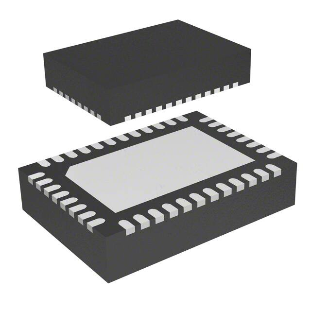
thermally enhanced compact, 5 mm × 7 mm, QFN
package. A 15-A output current capability makes the
device suitable for powering DSP and ASIC. The
device is designed to complement digital or analog
PWM controllers. The PWM input of the driver device
is 3-state compatible. Two driver circuits provide high
charge and discharge current for the high-side Nchannel FET switch and the low-side N-channel FET
synchronous rectifier in a synchronous buck
converter.
1
2
•
•
•
•
•
•
•
•
•
•
Integrates Synchronous Buck Driver and
NexFET™ Power MOSFET Technology for
High Power Density and High Efficiency
15-A Output Current Capability for DSP and
ASIC
4.7-V to 14-V Input Voltage Range
Operational Switching Frequency Up to 2 MHz
Built-In High-Side Current Protection
DCR Current Sensing for Overcurrent
Protection and Output Current Monitoring
Voltage Proportional to Load Current Monitor
Output
Tri-State PWM Input for Power Stage
Shutdown
UVLO Housekeeping Circuit
Integrated Thermal Shutdown
40-Pin, 5 mm x 7 mm, PQFN PowerStack™
Package
APPLICATIONS
•
•
Digital or Analog POL Power Modules
High Power Density DC-DC Converters for
Telecom and Networking Applications
A precision current sensing amplifier that processes
the voltage present across an external current sense
element measures and monitors the output current.
The PWM controller on the IMON pin can use this
amplified signal. On-board comparators monitor the
voltage across the high-side switch and the voltage
across the external current sense element to
safeguard the power stage from sudden high-current
loads. A single resistor for the high-side comparator
sets the blanking delay. This delay guards against
false reports coincident with switching edge noise. In
the event of a high-side fault or an overcurrent fault,
the high-side FET turns OFF and the fault flag (FLT)
asserts to alert the PWM controller.
APPLICATION DIAGRAM
From
Controller
SRE
To
Controller
PWM
FLT
VDD
HS_SNS
IMON
VIN
SRE_MD
BP3
UCD74111
BOOT
SW
ILIM
CSP
RDLY
CSN
AVGG
VGG_DIS AGND
VIN
VOUT
VGG
PGND
UDG-11243
1
2
Please be aware that an important notice concerning availability, standard warranty, and use in critical applications of
Texas Instruments semiconductor products and disclaimers thereto appears at the end of this data sheet.
NexFET, PowerStack are trademarks of Texas Instruments.
PRODUCTION DATA information is current as of publication date.
Products conform to specifications per the terms of the Texas
Instruments standard warranty. Production processing does not
necessarily include testing of all parameters.
Copyright © 2012, Texas Instruments Incorporated
�UCD74111
SLUSAT8 – OCTOBER 2012
www.ti.com
These devices have limited built-in ESD protection. The leads should be shorted together or the device placed in conductive foam
during storage or handling to prevent electrostatic damage to the MOS gates.
ORDERING INFORMATION (1)
(1)
TEMPERATURE
RANGE
PINS
PACKAGE
ORDERING NUMBER
–40°C to 125°C
40
RVF
UCD74111RVF
For the most current package and ordering information, see the Package Option Addendum at the end
of this document, or see the TI website at www.ti.com.
ABSOLUTE MAXIMUM RATINGS
over operating free-air temperature range (unless otherwise noted) (1)
VALUE
MIN
MAX
–0.3
16
V
SW DC
–1
16
V
SW Pulse < 400 ns, E = 20 µJ
–2
20
V
SW Pulse < 64 ns
–5
22
V
SW Pulse < 40 ns
–7
25
V
VGG, AVGG (Externally supplied)
–0.3
7
V
BOOT DC
–0.3
23
V
BOOT Pulse (SW at 20 V < 400 ns)
–0.3
27
V
BOOT Pulse (SW at 22 V < 64 ns)
–0.3
29
V
BOOT Pulse (SW at 25 V < 40 ns)
–0.3
32
V
ILIM, VGG_DIS, IMON, FLT
–0.3
3.6
V
CSP, CSN, RDLY, PWM, SRE, SRE_MD
–0.3
5.6
V
HS_SNS
–0.3
16
V
TJ
–40
150
°C
Tstg
–55
150
°C
VDD, VIN
Voltage range
Temperature
(1)
UNIT
Stresses beyond those listed under “absolute maximum ratings” may cause permanent damage to the device. These are stress ratings
only and functional operation of the device at these or any other condition beyond those included under “recommended operating
conditions” is not implied. Exposure to absolute-maximum-rated conditions for extended periods of time may affect device reliability.
THERMAL INFORMATION
UCD74111
THERMAL METRIC (1)
PQFN (RVF) 40PIN
θJA
Junction-to-ambient thermal resistance
28.9
θJCtop
Junction-to-case (top) thermal resistance
15.4
ψJT
Junction-to-top characterization parameter
0.2
ψJB
Junction-to-board characterization parameter
5.1
θJCbot
Junction-to-case (bottom) thermal resistance
0.8
(1)
2
UNITS
°C/W
For more information about traditional and new thermal metrics, see the IC Package Thermal Metrics application report, SPRA953.
Submit Documentation Feedback
Copyright © 2012, Texas Instruments Incorporated
�UCD74111
www.ti.com
SLUSAT8 – OCTOBER 2012
RECOMMENDED OPERATING CONDITIONS
MIN
VDD, VIN
TYP
MAX
4.7
14
UNIT
V
VGG, AVGG
Externally supplied gate drive voltage
4.6
6.5
V
TJ
Operating junction temperature
–40
125
°C
MAX
UNIT
ELECTROSTATIC DISCHARGE (ESD) PROTECTION
MIN
TYP
Human body model (HBM)
1.5
kV
Charge device model (CDM)
500
V
Copyright © 2012, Texas Instruments Incorporated
Submit Documentation Feedback
3
�UCD74111
SLUSAT8 – OCTOBER 2012
www.ti.com
ELECTRICAL CHARACTERISTICS
TJ = –40°C to 125°C, VVDD, VVIN = 12 V, all parameters at zero power dissipation (unless otherwise noted)
PARAMETER
TEST CONDITIONS
MIN
TYP
MAX
UNIT
INPUT SUPPLY
VVIN
Input supply voltage range
VVDD
IVDD
Supply current
4.7
Not switching, PWM = LOW
14
V
8
10
mA
4.4
4.6
V
GATE DRIVE UNDER-VOLTAGE LOCKOUT
VGG-ON
UVLO on voltage
VGG-OFF
UVLO off voltage
VGG-HYS
UVLO hysteresis voltage
4.1
4.3
V
80
mV
VGG SUPPLY GENERATOR
VGG
Output voltage
VVIN = 12 V, IGG = 50 mA
VDO
Dropout voltage, VVDD – VGG
VVIN = 4. 7V, IGG = 50 mA
5.3
6.0
6.8
V
350
mV
3.2
3.3
V
1.8
2.1
V
BP3 REGULATOR
VBP3
Output voltage
VVIN = 12 V, IBP3 = 2 mA
3.0
DIGITAL INPUT SIGNALS (PWM, SRE)
VIH-PWM
Positive-going input threshold voltage
VIL-PWM
Negative-going input threshold voltage
PWM
Input voltage hysteresis, (VIH – VIL)
VIH-SRE
Positive-going input threshold voltage
VIL-SRE
Negative-going input threshold voltage
SRE
Input voltage hysteresis, (VIH – VIL)
IPWM
Input current
0.8
Input current
(1)
tri-state hold-off time
V
1.7
V
1.0
0.45
V
140
VPWM = 3.3 V
70
VPWM = 0 V
–63
VSRE = 5 V
190
VSRE = 3.3 V
µA
12
VSRE = 0 V
tHLD-R
V
0.9
1.5
0.9
VPWM = 5 V
ISRE
0.9
µA
–330
VPWM transition from 0 V to 1.65 V,
time until low-side drive falls to 0 V
450
600
750
ns
OUTPUT CURRENT LIMIT (ILIM)
RILIM-IN (1)
ILIM input impedance
VILIM
ILIM set point range
VFLT-HI
FLT output high level
ILOAD = –2 mA
VFLT-LO
FLT output low level
ILOAD = 2 mA
0.1
0.6
V
tFAULT-FLT (1)
Fault detection time. Delay until FLT
asserted
VILIM = 1.5 V, (VCSP - VCSN) = 20 mV,
VCSN = 1.8 V
350
475
ns
tDLY (1)
Propagation delay from PWM to reset FLT
PWM falling to FLT falling after a current limit
event clears. PWM pulse width ≥ 100 ns
85
200
ns
8.06 kΩ resistor from RDLY to AGND
90
250
0.5
2.7
kΩ
3
3.3
V
V
CURRENT SENSE BLANKING (RDLY, HS_SNS)
IRDLY
RRDLY
RDLY source current
(1)
RDLY resistance range
tBLANK
HS_SNS blanking time
RRDLY = 8.06kΩ. From SW rising to HS fault
comparator enabled.
IOCH
Overcurrent threshold for high-side FET
TJ = 25°C, (VBOOT – VSW) = 5.5V
(1)
4
µA
5.00
8.06
25.00
kΩ
110
125
140
ns
30
A
Ensured by design. Not production tested.
Submit Documentation Feedback
Copyright © 2012, Texas Instruments Incorporated
�UCD74111
www.ti.com
SLUSAT8 – OCTOBER 2012
ELECTRICAL CHARACTERISTICS (continued)
TJ = –40°C to 125°C, VVDD, VVIN = 12 V, all parameters at zero power dissipation (unless otherwise noted)
PARAMETER
TEST CONDITIONS
MIN
TYP
MAX
0.46
0.50
0.54
UNIT
CURRENT SENSE AMPLIFIER (IMON, CSP, CSN)
VIMON
IMON voltage at no load
CSP = CSN = 1.8V
RCS-IN (2)
Input impedance
Differential, (VCSP - VCSN)
GCS
Closed loop DC gain
VCM (2)
100
(VCSP - VCSN) = 10 mV, 0.5 V ≤ VCSN ≤ 3.3 V
48
50.2
52.4
Gain with 2.49 kΩ resistors in series with
CSP, CSN
45.0
47.0
49.2
Input common mode voltage range
VCM maximum limit is (VVGG – 1.2 V)
–0.3
VIMON(min)
Minimum IMON voltage
VCSP = 1.2 V; VCSN = 1.3 V, IIMON = –250 µA
VIMON(max)
Maximum IMON voltage
VCSP = 1.3 V; VCSN = 1.2 V, IIMON = 500 µA
SR (2)
Sampling rate
3.0
V
kΩ
V/V
5.3
V
0.1
0.15
V
3.2
3.3
5
V
Msps
OUTPUT STAGE
RHI
High side device resistance
TJ = 25°C, VBOOT – VSW = 5.5 V
4.5
6.5
RLO
Low side device resistance
TJ = 25°C
1.9
2.7
Forward bias current 20 mA
0.4
mΩ
BOOTSTRAP DIODE
VF
Forward voltage
V
THERMAL SHUTDOWN
TTSD-R (2)
Rising threshold
155
165
175
°C
(2)
Falling threshold
135
145
155
ºC
TTSD-F
TTSD-HYS (2)
(2)
Hysteresis
20
ºC
Ensured by design. Not production tested.
Copyright © 2012, Texas Instruments Incorporated
Submit Documentation Feedback
5
�UCD74111
SLUSAT8 – OCTOBER 2012
www.ti.com
DEVICE INFORMATION
CSP
CSN
N/C
IMON
39
PWM
RDLY
40
Bp3
AVGG
RVF PACKAGE
40 PINS
(TOP VIEW)
38
37
36
35
34
33
AGND
1
32
ILIM
VGG_DIS
2
31
SRE
VGG
3
30
SRE_MD
N/C
4
29
FLT
BOOT
5
28
HS_SNS
N/C
6
27
VDD
SW
7
26
VIN
SW
8
25
VIN
SW
9
24
VIN
SW
10
23
VIN
SW
11
22
VIN
SW
12
21
VIN
14
15
16
17
18
19
20
PGND
PGND
PGND
PGND
PGND
PGND
PGND
13
PGND
Thermal Pad
The thermal pad functions as an electrical ground connection.
PIN FUNCTIONS
PIN
I/O
DESCRIPTION
NAME
NO.
AGND
1
AVGG
40
I/O
BOOT
5
Floating bootstrap supply for high side driver. Connect the bootstrap capacitor between this pin and the SW
I/O node. The bootstrap capacitor provides the charge to turn on the high-side FET. A low ESR ceramic capacitor
of 220 nF or greater from this pin to SW must be connected.
BP3
37
O
Output bypass for the internal 3.3V regulator. Connect a low ESR bypass ceramic capacitor of 1 µF or greater
from this pin to AGND.
CSN
35
I
Inverting input of the output current sense amplifier and current limit comparator.
CSP
36
I
Non-inverting input of the output current sense amplifier and current limit comparator.
Analog ground return for all circuits except the low-side gate driver. The analog ground and power ground
should be connected together at one point, near the AGND pin.
Voltage supply to internal control circuitry. Connect a low ESR bypass ceramic capacitor of 100 nF or greater
from this pin to AGND. Also a resistor of 1Ω to 2Ω must be connected between VGG and this pin.
FLT
29
O
Fault Flag. The FLT signal is a 3.3V digital output which asserts high when an overcurrent, over-temperature,
or UVLO fault is detected. After the device detects an overcurrent event, the flag resets to low on the falling
edge of the next pulse, provided the overcurrent condition no longer exists during the on-time of the PWM
signal. For UVLO and over-temperature faults, the flag is reset when the fault condition no longer exists.
HS_SNS
28
I
A 2-kΩ resistor must be connected from this pin directly to the drain of the high-side FET.
ILIM
32
I
Output current limit threshold set pin. The voltage on this pin sets the fault threshold voltage on the IMON pin.
The nominal threshold voltage range is 0.5 V to 3.0 V. When VIMON exceeds VILIM, the FLT pin is asserts and
the high-side gate pulse truncates.
IMON
33
O
Current sense linear amplifier output. The output voltage level on this pin represents the average output
current. V(IMON) = 0.5 V + 50.2(V(CSP) – V(CSN)).
4
N/C
6
Not internally connected.
34
6
Submit Documentation Feedback
Copyright © 2012, Texas Instruments Incorporated
�UCD74111
www.ti.com
SLUSAT8 – OCTOBER 2012
PIN FUNCTIONS (continued)
PIN
NAME
NO.
I/O
DESCRIPTION
13
14
15
PGND
16
Power ground pins. These pins provide a return path for low-side FET and the low-side gate driver.
17
18
19
20
PWM
38
I
PWM input. This pin is a digital input that accepts 3.3 V or 5 V logic level signals. A Schmitt trigger input
comparator desensitizes this pin from external noise. When SRE mode is high, this pin controls both gate
drivers. When SRE mode is low, this pin only controls the high-side driver. This pin can detect when the input
drive signal has switched to a high impedance (tri-state) mode. When the high impedance mode is detected,
both the high-side gate and low-side gate signals are held low.
RDLY
39
I
Requires a resistor to AGND for setting the current sense blanking time for the high-side current sense
comparator and output current limit circuitry.
I
Synchronous rectifier enable or low-side input. This pin is a digital input capable of accepting 3.3V or 5V logic
level signals. A Schmitt trigger input comparator desensitizes this pin from external noise. When SRE mode is
high, this signal, when low, disables the synchronous rectifier FET. The low-side gate signal is held off. When
SRE mode is high, this signal, when high, allows the low-side gate signal to function according to the state of
the PWM pin. When SRE mode is low, this pin is a direct input to the low-side gate driver.
I
Synchronous rectifier enable mode select pin. When pulled high to BP3, the high-side and low-side gate drive
timing is controlled by the PWM pin. Anti-cross-conduction logic prevents simultaneous application of high-side
and low-side gate drive. When pulled low to AGND, independent operation of the high-side and low-side gate is
selected. The high-side gate is directly controlled by the PWM signal. The low-side gate is directly controlled by
the SRE signal. No anti-cross-conduction circuitry is active in this mode. This pin should not be left floating.
SRE
SRE_MD
31
30
7
8
SW
9
10
I/O
Sense line for the adaptive anti-cross conduction circuitry. Serves as common connection for the flying high
side FET driver.
I
Input voltage to internal driver circuitry and control circuitry. Connect a low ESR bypass ceramic capacitor of
100 nF or greater from this pin to AGND.
11
12
VDD
27
VGG
3
VGG_DIS
2
I
VGG disable pin. When pulled high to BP3, the on-chip VGG linear regulator is disabled. When disabled, an
externally supplied gate voltage must be connected to the VGG pin. Connect this pin to AGND to use the onchip regulator.
21–26
I
Power input to the high-side FET.
VIN
Thermal Pad
Gate drive voltage supply. When VGG_DIS is low, VGG is generated by an on-chip linear regulator. Nominal
I/O output voltage is 6.4 V. When VGG_DIS is high, an externally supplied gate voltage can be applied to this pin.
Connect a 4.7 µF low ESR ceramic capacitor from this pin to PGND.
Power Pad for better thermal performance. It is also connected to PGND internally.
Copyright © 2012, Texas Instruments Incorporated
Submit Documentation Feedback
7
�UCD74111
SLUSAT8 – OCTOBER 2012
www.ti.com
BLOCK DIAGRAM
VDD
AVGG VGG
RDLY
Bias
VGG/AVGG
Generator
VGG/AVGG
Blanking
Control
BP3
VGG_DIS
UVLO
PWM
HS Fault
SRE
HS_SNS
BOOT
VIN
+
Digital
Control
SRE_MD
FLT
SW
Thermal
Sense
ILIM
PGND
+
0.5 V
+
IMON
CSP
+
CSN
UCD74111
AGND
8
Submit Documentation Feedback
Thermal Pad
UDG-11244
Copyright © 2012, Texas Instruments Incorporated
�UCD74111
www.ti.com
SLUSAT8 – OCTOBER 2012
DETAILED DESCRIPTION
Introduction
The UCD74111 is a power stage for synchronous buck converter with current measurement and fault detection
capabilities making it an ideal partner for digital power controllers. This device incorporates two high-current gate
drive stages, two high-performance NexFET power MOSFETs, and sophisticated current measurement circuitry
that allows for the monitoring and reporting of output load current. Two separate fault detection blocks protect the
power stage from excessive load current or short circuits. On-chip thermal shutdown protects the device in case
of severe over-temperature conditions. The device detects faults immediately, truncates the power conversion
cycle in progress, without controller intervention, and asserts a digital fault flag (FLT). An on-chip linear regulator
supplies the gate drive voltage. If desired, this regulator can be disabled and an external gate drive voltage can
be supplied. Mode selection pins allow the device to be used in synchronous mode or independent mode. In
synchronous mode, the high-side and low-side gate timing is controlled by a single PWM input. Anti-crossconduction dead-time intervals are applied automatically to the gate drives. The PWM and SRE pins directly
controls the high-side and low-side gate drive signals In independent mode. The automatic dead-time logic is
disabled in this mode. When operating in synchronous mode, the use of the low-side FET can be disabled under
the control of the SRE pin. This feature facilitates start-up into a pre-bias voltage and is also used in some
applications to reduce power consumption at light loads.
PWM Input (PWM)
The PWM input pin accepts the digital signal from the controller that represents the desired high-side FET ontime duration. This input accepts 3.3-V logic levels, but also tolerates 5-V input levels. The SRE mode pin sets
the behavior of the PWM pin. When the SRE mode pin asserts high, the device goes into in synchronous mode.
In this mode, PWM input signal controls both the timing duration of the high-side gate drive and the low-side gate
drive . When PWM is high, the high-side gate drive (HS Gate) is on and the low-side gate drive is off. When
PWM is low, the high-side gate drive is off and the low-side gate drive is on. Automatic anti-cross-conduction
logic monitors the gate to source voltage of the FETs to verify that the proper FET is turned OFF before the other
FET is turned ON. When the SRE mode pin is asserted low, the device goes into independent mode. In this
mode the PWM input controls the high-side gate drive only. When PWM is high, the high-side gate drive is on.
While in independent mode, the SRE pin directly controls the low-side FET. Independent mode does not activate
any anti-cross-conduction logic. The user must ensure that the PWM and SRE signals do not overlap.
The PWM input supports a tri-state detection feature. It detects when the PWM input signal has entered a tristate mode. When the device detects a tri-state mode, both the high-side and low-side gate drive signals remain
OFF. To support this mode, the PMW input pin has an internal pull-up resistor of approximately 50 kΩ connected
to the 3.3 V input. It also has a 50 kΩ pull-down resistor to ground. During normal operation, the PWM input
signal swings below 0.8 V and above 2.5 V. If the source driving the PWM pin enters a tri-state or high
impedance state, the internal pull-up/pull-down resistors tends to pull the voltage on the PWM pin to 1.65 V. If
the voltage on the PWM pin remains within the 0.8 V to 2.5 V tri-state detection range for longer than the tri-state
detection hold-off time (tHLD_R), then the device enters tri-state mode and turns both gate drives OFF. This
behavior occurs regardless of the state of the SRE mode and SRE pins. When exiting tri-state mode, PWM
should first be asserted low. This ensures that the bootstrap capacitor is recharged before attempting to turn on
the high-side FET.
The logic threshold of this pin typically exhibits 900 mV of hysteresis to provide noise immunity and ensure glitchfree operation of the gate drivers.
Copyright © 2012, Texas Instruments Incorporated
Submit Documentation Feedback
9
�UCD74111
SLUSAT8 – OCTOBER 2012
www.ti.com
Synchronous Rectifier Enable Input (SRE)
The SRE (synchronous rectifier enable) pin is a digital input with an internal ,10-kΩ, pull-up resistor connected to
the 3.3-V input. It is designed to accept 3.3-V logic levels, but is also tolerant of 5-V levels. The SRE mode pin
sets the behavior of the SRE pin. When the SRE mode pin is asserted high, the device enters synchronous
mode. In synchronous mode, the input, when asserted high, enables the operation of the low-side synchronous
rectifier FET. The PWM input controls the state of the low-side gate drive signal . When SRE is asserted low
while in synchronous mode, the low-side FET gate drive holds low, keeping the FET off. While remaining OFF,
the low-side FET restricts the current flow to the intrinsic body diode. When the SRE mode pin is asserted low,
the device enters independent mode. In independent mode, the state of the low-side gate drive signal follows the
state of the SRE signal. It is completely independent of the state of the PWM signal. No anti-cross-conduction
logic is active in independent mode. The user must ensure that the PWM and SRE signals do not overlap.
The logic threshold of this pin typically exhibits 450 mV of hysteresis to provide noise immunity and ensure glitchfree operation of the low-side gate driver.
SRE Mode (SRE_MD)
The SRE mode pin is a digital input that accept 3.3-V logic levels, and levels up to 5-V. The SRE pin sets the
operational mode on the device. When asserted high, the device enters synchronous mode. In synchronous
mode, the PWM input controls the behavior of both the high-side and low-side gate drive signals. When asserted
low, this pin configures the device for independent mode. In independent mode the PWM pin controls the highside FET and the SRE pin controls the low-side FET. The SRE mode pin should be s permanently tied high or
low depending on the power architecture being implemented. It not intended to be switched dynamically while the
device is in operation. This pin can be tied to the BP3 pin to always select synchronous mode.
Input Voltage for Internal Circuits (VDD)
The VDD pin supplies power to the internal circuits of the device. An internal linear regulator that provides the
VVGG gate drive voltage conditions the input power . A second regulator that operates off of the VVGG rail
produces an internal 3.3-V supply that powers the internal analog and digital functional blocks. The BP3 pin
provides access for a high frequency bypass capacitor on this internal rail. The VGG regulator produces a
nominal output of 6.4 V. The undervoltage lockout (UVLO) circuitry monitors the output of the VGG regulator.
The device does not attempt to produce gate drive pulses until the VGG voltage is above the UVLO threshold.
This delay ensures that there is sufficient voltage available to drive the power FETs into saturation when
switching activity begins.
Voltage Supply for Gate Drive and Internal Control Circuitry (VGG and AVGG)
The VGG pin is the gate drive voltage for the high current gate drive stages. The AVGG pin is the voltage supply
to internal control circuitry. The on-chip regulator can supply the voltage internally on the VGG pin, or the user
can supply the voltage externally.. When using the internal regulator, the VGG_DIS pin should be tied low. When
an external source of VGG is to be used, the VGG_DIS pin must be tied high. Current is drawn from the VGG
supply in fast, high-current pulses. Connect s 4.7-µF ceramic capacitor between the VGG pin and PGND pin as
close as possible to the package.
Connect a resistor with a value between 1 Ω and 2 Ω between the AVGG pin and the VGG pin. A low ESR
bypass ceramic capacitor of 100 nF or greater needs to be connected from AVGG pin to AGND as well.
Whether the voltage is internally or externally supplied, UVLO circuitry monitors the voltage on the VGG pin. The
voltage must be higher than the UVLO threshold before power conversion can occur. Note that the FLT pin is
asserted high when VVGG is below the UVLO threshold.
VGG Disable (VGG_DIS)
The VGG_DIS pin, when asserted high, disables the on-chip VGG linear regulator. When tied low, the VGG
linear regulator is derives the VGG supply from VIN. Permanently tie the VGG_DIS pin high or low depending on
the power architecture being implemented. The VGG_DIS pin should not be switched dynamically while the
device is in operation.
10
Submit Documentation Feedback
Copyright © 2012, Texas Instruments Incorporated
�UCD74111
www.ti.com
SLUSAT8 – OCTOBER 2012
Switching Node (SW)
The SW pin connects to the switching node of the power conversion stage. It acts as the return path for the highside gate driver. When configured as a synchronous buck stage, the voltage swing on SW normally traverses
from below ground to well above VIN. Parasitic inductance in the high-side FET and the output capacitance
(COSS) of both power FETs form a resonant circuit that can produce high frequency ( > 100 MHz) ringing on this
node. The voltage peak of this ringing, if not controlled, can be significantly higher than VIN. Ensure that no peak
ringing amplitude exceeds the absolute maximum rating limit for the pin.
In many cases, connecting a series resistor and capacitor snubber network connected from the switching node to
PGND can dampen the ringing and decreasing the peak amplitude. Make sllowanced for snubber network
components during the layout of the printed circuit board. If testing reveals that the ringing amplitude at the SW
pin exceeds the limit, then populate the snubber components.
Placing a BOOT resistor with a value between 5 Ω and 10 Ω in series with the BOOT capacitor slows down the
turn-on of the high-side FET and can help to reduce the peak ringing at the switching node as well.
Bootstrap (BST)
The BST pin provides the drive voltage for the high-side FET. A bootstrap capacitor connects his pin to the SW
node. Internally, a diode connects the BST pin to the VGG supply. In normal operation, when the high-side FET
is off and the low-side FET is on, the SW node is pulled to ground and, thus, holds one side of the bootstrap
capacitor at ground potential. The other side of the bootstrap capacitor is clamped by the internal diode to VGG.
The voltage across the bootstrap capacitor at this point is the magnitude of the gate drive voltage available to
switch-on the high-side FET. The bootstrap capacitor should be a low ESR ceramic type, with a recommended
minimum value of 0.22 µF. The recommended minimum voltage rating is 16 V or higher.
Current Sense (CSP, CSN)
The CSP and CSN pins are the input to the differential current sense amplifier. The current sense positive (CSP)
pin connects to the non-inverting input, the current sense negative (CSN) connects to the inverting input. This
amplifier provides the means to monitor and measure the output current of the power stage. The circuitry can be
used with a discrete, low value, series current sense resistor, or can make use of the popular inductor DCR
sense method.
Figure 1 illustrates the DCR method of currnet sensing . A series resistor and capacitor network is added across
the buck stage power inductor. When the value of L/DCR is equal to RC, then the voltage developed across the
capacitor, C, is a replica of the voltage waveform the ideal current would induce in the dc resistance (DCR) of the
inductor. This method does not detect changes in current due to changes in inductance value caused by
saturation effects. The value used for C should be between 0.1 µF and 2.2 µF. This maintains a low impendence
of the sense network, which reduces its susceptibility to noise pickup from the switching node. The trace lengths
of the CSP and CSN signals should be kept short and parallel. To aid in rejection of high frequency commonmode noise, a series 2.49-kΩ resistor should be added to both the CSP and CSN signal paths, with the resistors
being placed close to the pins at the package. This small amount of additional resistance slightly lowers the
current sense gain.
Select power inductors with the lowest possible DCR in order to minimize losses. Typical DCR values range
between 0.5 mΩ and 5 mΩ. With a load current of 15 A, the voltage presented across the CSP and CSN pins is
between 7.5 mV and 75 mV. Note that this small differential signal is superimposed on a large common mode
signal that is the dc output voltage. This makes the current sense signal challenging to process.
The UCD74111 uses switched capacitor technology to perform the differential to single-ended conversion of the
sensed current signal. This technique offers excellent common mode rejection. The differential CSP-CSN signal
is amplified by a factor of 47 and then a fixed 500-mV pedestal voltage is added to the result. This signal is
presented to the IMON pin.
When using inductors with DCR values of 2.0 mΩ or higher, it may be necessary to attenuate the input signal to
prevent saturation of the current sense amplifier. Add of resistor R2 as shown in Figure 2 to provide attenuation.
Copyright © 2012, Texas Instruments Incorporated
Submit Documentation Feedback
11
�UCD74111
SLUSAT8 – OCTOBER 2012
www.ti.com
L
L
DCR
DCR
SW
VOUT
R
SW
VOUT
R1
C
2.49 kW
C
R2
2.49 kW
2.49 kW
CSP
2.49 kW
CSN
UDG-11183
CSP
CSN
UDG-11184
Figure 1. DCR Current Sense
Figure 2. Attenuating the DCR Sense Signal
The amount of attenuation is equal to R2/(R1 + R2). The equivalent resistance value to use in the L/DCR = RC
formula is the parallel combination of R1 and R2. Thus, when using the circuit shown in Figure 2,
L
C ´ R1´ R2
=
DCR
(R1 + R2 )
(1)
Current Monitor (IMON)
The IMON pin signal is a voltage proportional to the output current delivered by the power stage. Figure 1
describes the voltage magnitude when using the circuit shown in Figure 1.. Equation 2 reflects the gain reduction
caused by the series 2.49-kΩ resistors.
V (IOUT ) = 0.5 + 47 ´ DCR ´ ILOAD
(2)
If the calculated value of VIMON at maximum load exceeds 2.5 V, then the circuit of Figure 2 should be used.
When using the circuit shown in Figure 2, the modified Equation 3 describes the voltage on IMON.
æ R2 ö
V (IOUT ) = 0.5 + 47 ´ DCR ´ ILOAD ´ ç
÷
è R1 + R2 ø
(3)
In either case, the output voltage is 500 mV at no load. Current that is sourced to the load causes the IMON
voltage to rise above 500 mV. Current that is forced into the power stage (sinking current) is considered negative
current and causes the IMON voltage to fall below 500 mV. The usable dynamic range of the IMON signal is
approximately 100 mV to 3.1 V. Note that this signal swing could exceed not just the maximum range of an
analog to digital converter (ADC) that may be used to read or monitor the IMON signal, but also the maximum
programmable limit for the fault OC threshold. For example, the UCD92xx family of digital controllers has
maximum limit of 2.5 V for the ADC converter and 2.0 V for the fault overcurrent threshold, even though the input
pin can tolerate voltages up to 3.3 V.
The device internally feeds the IMON voltage (VIMON) to the non-inverting input of the output overcurrent fault
comparator. Set the overcurrent threshold to approximately 150% of the rated power stage output current plus
one half of the peak-to-peak inductor ripple current.. This setting requires that the IMON signal remain within its
linear dynamic range at this threshold load current level. This requirement may force the use of the attenuation
circuit of Figure 2. Note that the IMON voltage (that goes to the output overcurrent fault comparator) is held
during the blanking interval set by the resistor on the RDLY pin. This means that the IMON pin does not reflect
output current changes during the blanking interval, and that a fault is not flagged until the blanking interval
terminates.
Current Limit (ILIM)
The ILIM pin feeds the inverting input of the output overcurrent fault comparator. The voltage applied to this pin
sets the overcurrent fault threshold. When the voltage on the IMON pin exceeds the voltage on this pin, a fault is
flagged. The voltage on this pin can be set by a voltage divider, a DAC, or by a filtered PWM output. The usable
voltage range of the ILIM pin is approximately 0.6V to 3.1V. This represents the linear range of the IMON signal
for sourced output current. When using a voltage divider to set the threshold, a small (0.01µF) capacitor to BP3
can be added to improve noise immunity.
12
Submit Documentation Feedback
Copyright © 2012, Texas Instruments Incorporated
�UCD74111
www.ti.com
SLUSAT8 – OCTOBER 2012
Blanking Time (RDLY)
The RDLY pin sets the blanking time of the high-side fault detection comparator. A resistor to AGND sets the
blanking time according to the following formula, where tBLANK is in nanoseconds and RDLY is in kΩ. Do not use
a value greater than 25 kΩ for the RDLY resistor.
RRDLY =
(tBLANK - 54.4 )
8.76
(4)
To calculate the nominal blanking time for a given value of resistance, use Equation 5.
tBLANK = 8.76 ´ RRDLY + 54.4
(5)
The blanking interval begins on the rising edge of SW. During the blanking time the high-side fault comparator is
held off. A high-side fault is flagged when the voltage drop across the high-side FET exceeds the threshold set
by the HS_SNS pin. Blanking is required because the high amplitude ringing that occurs on the rising edge of
SW would otherwise cause false triggering of the fault comparator. The required amount of blanking time is a
function of the high-side FET, the PCB layout, and whether or not a snubber network is being used. A value of
100 ns is a typical starting point. An RRDLY of 8.06 kΩ provides 125 ns of blanking. Maintains a blanking interval
as short as possible, consistent with reliable fault detection. The blanking interval sets the minimum duty cycle
pulse width where high-side fault detection is possible. When the duty-cycle of the PWM pulses are narrower
than the blanking time, the high-side fault detection comparator is held off for the entire on-time and is, therefore,
blind to any high-side faults.
Internally, a 90-µA current source supplies the RDLY. When using the default value of 8.06 kΩ, the voltage
measured on the RDLY pin is approximately 725 mV.
Fault Flag (FLT)
The fault flag (FLT) is a digital output pin that asserts when a significant fault is detected. It alerts the host
controller to an event that has interrupted power conversion. The device holds the FLT pin low in normal
operation.
When a fault is detected, the FLT pin asserts high (3.3 V). There are four events that can trigger the FLT signal:
• output overcurrent
• high-side overcurrent
• undervoltage lockout (UVLO)
• thermal shutdown
The Fault Behavior section describes operation of the device during fault conditions. When asserted in response
to an overcurrent fault, the FLT signal is reset low upon the falling edge of a subsequent PWM pulse, provided
no faults are detected during the on-time of the pulse. If the fault is still present, the flag remains asserted. When
asserted in response to an UVLO or thermal shutdown event, the FLT pin automatically de-asserts itself when
the UVLO or thermal event has passed. If the on-time of the PWM pulse is less than 100 ns, then more than one
pulse may be required to reset the flag.
3.3-V BP Regulator (BP3)
The BP3 pin provides a connection point for a bypass capacitor that quiets the internal 3.3-V voltage rail.
Connect a 1-µF (or greater) ceramic capacitor from this pin to analog ground. Do not draw current from this pin.
The BP3 pin is not intended to be a significant source of 3.3-V input voltage. However, the user can design an
application that includes 3.3-V source for an ILIM voltage divider and a tie point for the SRE mode pin. Limit the
current drawn 100 µA or less.
Fault Behavior
When faults are detected, the device reacts immediately to minimize power dissipation in the FETs and protect
the system. The type of fault influences the behavior of the gate drive signals.
Immediately after a thermal shutdown fault occurs, the device forces both high-side gate and low-side gate low.
They remain low (regardless of the state of the PWM and the SRE pin) for the duration of the thermal shutdown.
Copyright © 2012, Texas Instruments Incorporated
Submit Documentation Feedback
13
�UCD74111
SLUSAT8 – OCTOBER 2012
www.ti.com
A UVLO fault occurs when the voltage on the VGG pin is less than the UVLO threshold. During this time both the
high-side gate and low-side gate are driven low, regardless of the state of PWM and SRE. The fault
automatically cleares when VVGG rises above the UVLO threshold.
When the device detects either a high-side fault or an output overcurrent fault, the FLT pin asserts high, and the
device immediately pulls both gate signals to low. During a high-side fault, the device issues a high-side gate
pulse with each incoming PWM pulse. If the fault is still present, the high-side gate signal again truncates. This
behavior repeats on a cycle-by-cycle basis until the fault clears or the PWM input remains low. Figure 3
illustrates this behavior.
PWM
Fault Detected
FLT
HS Gate
LS Gate
Figure 3. High-side Overcurrent Fault Response
When the device detects a high-side fault and output overcurrent fault concurrently, then it immediately turns
OFF and holds OFF both FET drives. If the output overcurrent fault remains present at the next PWM rising
edge, then the device issues no high-side gate pulsecontinue to be hold both gates OFF. Unlike the high-side
fault detection circuitry, the output overcurrent fault circuitry does not reset on a cycle-by-cycle basis. The output
current must fall below the overcurrent threshold before switching resumes.
FLT Reset
With the exception of a UVLO fault or a thermal shutdown fault, subsequent PWM pulses clears the FLT flag,
after it is asserted. The device clears the FLT flag at the falling edge of the next PWM pulse, provided a fault
condition is not asserted during the entire on-time of the PWM pulse. If the device detects a fault during the ontime interval, the FLT pin remains asserted. Figure 4 illustrates this behavior.
PWM
Fault
detected
Fault
remains
Internal
Fault Signal
FLT
No fault present during entire
PWM high interval. FLT reset
on PWM falling edge
Figure 4. FLT Reset Sequence
14
Submit Documentation Feedback
Copyright © 2012, Texas Instruments Incorporated
�UCD74111
www.ti.com
SLUSAT8 – OCTOBER 2012
Whenever the voltage on the VGG pin is below the UVLO falling threshold, as at the time of initial power-up, for
example, the FLT pin asserts. When the voltage on the VGG pin rises above the UVLO rising threshold, the
device clears the FLT automatically. This feature permits the FLT pin to be used as a power not good signal at
initial power-up to signify that there is insufficient gate drive voltage available to permit proper power conversion.
When FLT goes low, it is an indication of gate drive power good and power conversion can commence. After
initial power-up, the assertion of the FLT flag should be interpreted that power conversion has stopped or has
been limited by a fault condition.
Thermal Shutdown
If the junction temperature exceeds approximately 165°C, the device enters thermal shutdown. This asserts the
FLT pin and both gate drivers are turned OFF. When the junction temperature cools by approximately 20°C, the
device exits thermal shutdown. The FLT flag resets upon exiting thermal shutdown.
Copyright © 2012, Texas Instruments Incorporated
Submit Documentation Feedback
15
�PACKAGE OPTION ADDENDUM
www.ti.com
10-Dec-2020
PACKAGING INFORMATION
Orderable Device
Status
(1)
Package Type Package Pins Package
Drawing
Qty
Eco Plan
(2)
Lead finish/
Ball material
MSL Peak Temp
Op Temp (°C)
Device Marking
(3)
(4/5)
(6)
UCD74111RVFR
ACTIVE
LQFN-CLIP
RVF
40
3000
RoHS-Exempt
& Green
NIPDAU
Level-2-260C-1 YEAR
-40 to 125
UCD74111
UCD74111RVFT
ACTIVE
LQFN-CLIP
RVF
40
250
RoHS-Exempt
& Green
NIPDAU
Level-2-260C-1 YEAR
-40 to 125
UCD74111
(1)
The marketing status values are defined as follows:
ACTIVE: Product device recommended for new designs.
LIFEBUY: TI has announced that the device will be discontinued, and a lifetime-buy period is in effect.
NRND: Not recommended for new designs. Device is in production to support existing customers, but TI does not recommend using this part in a new design.
PREVIEW: Device has been announced but is not in production. Samples may or may not be available.
OBSOLETE: TI has discontinued the production of the device.
(2)
RoHS: TI defines "RoHS" to mean semiconductor products that are compliant with the current EU RoHS requirements for all 10 RoHS substances, including the requirement that RoHS substance
do not exceed 0.1% by weight in homogeneous materials. Where designed to be soldered at high temperatures, "RoHS" products are suitable for use in specified lead-free processes. TI may
reference these types of products as "Pb-Free".
RoHS Exempt: TI defines "RoHS Exempt" to mean products that contain lead but are compliant with EU RoHS pursuant to a specific EU RoHS exemption.
Green: TI defines "Green" to mean the content of Chlorine (Cl) and Bromine (Br) based flame retardants meet JS709B low halogen requirements of


 工商网监
湘ICP备2023018690号
工商网监
湘ICP备2023018690号
