CY14B256K
256 Kbit (32K x 8) nvSRAM with Real Time Clock
Features
■
High reliability
❐ Endurance to 200K cycles
❐ Data retention: 20 years at 55°C
■
25 ns, 35 ns, and 45 ns access times
■
Pin compatible with STK17T88
■
Single 3V operation with tolerance of +20%, -10%
■
Data integrity of Cypress nvSRAM combined with full featured
Real Time Clock
❐ Low power, 350 nA RTC current
❐ Capacitor or battery backup for RTC
■
Commercial and industrial temperature
■
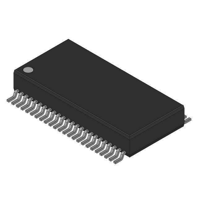
48-Pin SSOP (ROHS compliant)
■
Watchdog timer
■
Clock alarm with programmable interrupts
■
Hands off automatic STORE on power down with only a small
capacitor
■
STORE to QuantumTrap™ initiated by software, device pin, or
on power down
■
RECALL to SRAM initiated by software or on power up
■
Infinite READ, WRITE, and RECALL cycles
Functional Description
The Cypress CY14B256K combines a 256 Kbit nonvolatile static
RAM with a full-featured real time clock in a monolithic integrated
circuit. The embedded nonvolatile elements incorporate
QuantumTrap technology producing the world’s most reliable
nonvolatile memory. The SRAM is read and written an infinite
number of times, while independent, nonvolatile data resides in
the nonvolatile elements.
The real time clock function provides an accurate clock with leap
year tracking and a programmable high accuracy oscillator. The
alarm function is programmable for one time alarms or periodic
seconds, minutes, hours, or days. There is also a programmable
watchdog timer for process control.
Logic Block Diagram
VCC
QuantumTrap
512 X 512
A5
A9
A 11
A 12
A 13
POWER
CONTROL
STORE
ROW DECODER
A6
A7
A8
STATIC RAM
ARRAY
512 X 512
RECALL
DQ 4
DQ 5
DQ 6
HSB
A13
- A0
COLUMN IO
INPUT BUFFERS
DQ 2
VRTCcap
SOFTWARE
DETECT
DQ 0
DQ 3
VRTCbat
STORE/
RECALL
CONTROL
A 14
DQ 1
VCAP
COLUMN DEC
RTC
x1
x2
MUX
A14
INT
A 0 A 1 A 2 A 3 A 4 A 10
DQ 7
- A0
OE
CE
WE
Cypress Semiconductor Corporation
Document Number: 001-06431 Rev. *H
•
198 Champion Court
•
San Jose, CA 95134-1709
•
408-943-2600
Revised February 24, 2009
[+] Feedback
�CY14B256K
Pin Configurations
Figure 1. 48-Pin SSOP
V CAP
1
48
V CC
NC
A 14
2
47
NC
3
46
HSB
4
45
5
44
WE
A 13
A 12
A7
A6
6
43
A5
7
42
A9
INT
8
41
NC
A4
9
NC
10
NC
11
NC
V SS
12
NC
14
13
A8
48-SSOP
40
A 11
39
NC
38
NC
Top View
37
NC
36
(Not To Scale)
V SS
35
NC
V RTCcap
V RTCbat
15
34
DQ0
16
33
DQ 6
A3
17
32
A2
18
31
OE
A 10
A1
19
30
A0
CE
20
29
DQ7
DQ5
DQ1
21
28
DQ2
22
27
DQ4
X1
23
26
DQ3
X2
24
25
V CC
Pin Definitions
Pin Name
Alt
A0–A14
IO Type
Input
DQ0-DQ7
Description
Address Inputs. Used to select one of the 32,768 bytes of the nvSRAM.
Input or Output Bidirectional Data IO lines. Used as input or output lines depending on operation.
NC
No Connect
WE
W
Input
Write Enable Input, Active LOW. When the chip is enabled and WE is LOW, data on the IO
pins is written to the specific address location.
CE
E
Input
Chip Enable Input, Active LOW. When LOW, selects the chip. When HIGH, deselects the chip.
OE
G
Input
Output Enable, Active LOW. The active LOW OE input enables the data output buffers during
read cycles. Deasserting OE high causes the IO pins to tri-state.
X1
Output
No Connects. This pin is not connected to the die.
Crystal Connection. Drives crystal on start up.
X2
Input
VRTCcap
Power Supply
Crystal Connection for 32.768 kHz Crystal.
Capacitor Supplied Backup RTC Supply Voltage. (Left unconnected if VRTCbat is used)
VRTCbat
Power Supply
Battery Supplied Backup RTC Supply Voltage. (Left unconnected if VRTCcap is used)
INT
Output
Interrupt Output. It is programmed to respond to the clock alarm, the watchdog timer, and the
power monitor. Programmable to either active HIGH (push or pull) or LOW (open drain).
Ground for the Device. It is connected to ground of the system.
VSS
Ground
VCC
Power Supply
HSB
Input or Output Hardware Store Busy (HSB). When low, this output indicates a Hardware Store is in progress.
When pulled low external to the chip, it initiates a nonvolatile STORE operation. A weak internal
pull up resistor keeps this pin HIGH if not connected (connection optional).
VCAP
Power Supply
Power Supply Inputs to the Device.
AutoStore Capacitor. Supplies power to nvSRAM during power loss to store data from SRAM
to nonvolatile elements.
Document Number: 001-06431 Rev. *H
Page 2 of 28
[+] Feedback
�CY14B256K
Device Operation
automatically disconnects the VCAP pin from VCC. A STORE
operation is initiated with power provided by the VCAP capacitor.
The CY14B256K nvSRAM consists of two functional
components paired in the same physical cell. The components
are SRAM memory cell and a nonvolatile QuantumTrap cell. The
SRAM memory cell operates as a standard fast static RAM. Data
in the SRAM is transferred to the nonvolatile cell (the STORE
operation), or from the nonvolatile cell to SRAM (the RECALL
operation). Using this unique architecture, all cells are stored and
recalled in parallel. During the STORE and RECALL operations,
SRAM READ and WRITE operations are inhibited. The
CY14B256K supports infinite reads and writes similar to a typical
SRAM. In addition, it provides infinite RECALL operations from
the nonvolatile cells and up to 200K STORE operations.
Figure 2. AutoStore Mode
V CC
0.1UF
10k Ohm
V CAP
V CAP
V CC
WE
See the “Truth Table For SRAM Operations” on page 22 for a
complete description of read and write modes.
SRAM READ
The CY14B256K performs a READ cycle whenever CE and OE
are LOW while WE and HSB are HIGH. The address specified
on pins A0-14 determines which of the 32,752 data bytes are
accessed. When the READ is initiated by an address transition,
the outputs are valid after a delay of tAA (see the section Figure
8 on page 17). If the READ is initiated by CE or OE, the outputs
are valid at tACE or at tDOE, whichever is later (see the section
Figure 9 on page 17). The data outputs repeatedly respond to
address changes within the tAA access time without the need for
transitions on any control input pins. This remains valid until
another address change or until CE or OE is brought HIGH, or
WE or HSB is brought LOW.
SRAM WRITE
A WRITE cycle is performed whenever CE and WE are LOW and
HSB is HIGH. The address inputs are stable before entering the
WRITE cycle and must remain stable until either CE or WE goes
HIGH at the end of the cycle. The data on the common IO pins
DQ0–7 is written into the memory if the data is valid tSD before
the end of a WE controlled WRITE or before the end of a CE
controlled WRITE. Keep OE HIGH during the entire WRITE cycle
to avoid data bus contention on common IO lines. If OE is left
LOW, internal circuitry turns off the output buffers tHZWE after WE
goes LOW.
AutoStore® Operation
The CY14B256K stores data to nvSRAM using one of the three
storage operations:
1. Hardware store activated by HSB
2. Software store activated by an address sequence
3. AutoStore on device power down
AutoStore operation is a unique feature of QuantumTrap
technology and is enabled by default on the CY14B256K.
During normal operation, the device draws current from VCC to
charge a capacitor connected to the VCAP pin. This stored
charge is used by the chip to perform a single STORE operation.
If the voltage on the VCC pin drops below VSWITCH, the part
Figure 2 shows the proper connection of the storage capacitor
(VCAP) for automatic store operation. Refer to DC Electrical
Characteristics on page 15 for the size of the VCAP. The voltage
on the VCAP pin is driven to 5V by a charge pump internal to the
chip. A pull up should be placed on WE to hold it inactive during
power up. This pull up is only effective if the WE signal is tri-state
during power up. Many MPUs tri-state their controls on power up.
Verify this when using the pull up. When the nvSRAM comes out
of power-on-recall, the MPU must be active or the WE held
inactive until the MPU comes out of reset.
To reduce unnecessary nonvolatile stores, AutoStore and
Hardware Store operations are ignored unless at least one
WRITE operation has taken place since the most recent STORE
or RECALL cycle. Software initiated STORE cycles are
performed regardless of whether a WRITE operation has taken
place. The HSB signal is monitored by the system to detect if an
AutoStore cycle is in progress.
Hardware STORE (HSB) Operation
The CY14B256K provides the HSB pin for controlling and
acknowledging the STORE operations. The HSB pin is used to
request a hardware STORE cycle. When the HSB pin is driven
low, the CY14B256K conditionally initiates a STORE operation
after tDELAY. An actual STORE cycle only begins if a WRITE to
the SRAM takes place since the last STORE or RECALL cycle.
The HSB pin also acts as an open drain driver that is internally
driven low to indicate a busy condition, while the STORE
(initiated by any means) is in progress. This pin is externally
pulled up if it is used to drive other inputs.
SRAM READ and WRITE operations, that are in progress when
HSB is driven low by any means, are given time to complete
before the STORE operation is initiated. After HSB goes LOW,
the CY14B256K continues SRAM operations for tDELAY. During
Document Number: 001-06431 Rev. *H
Page 3 of 28
[+] Feedback
�CY14B256K
tDELAY, multiple SRAM READ operations take place. If a WRITE
is in progress when HSB is pulled LOW, it allows a time, tDELAY,
to complete. However, any SRAM WRITE cycles requested after
HSB goes LOW are inhibited until HSB returns HIGH.
It is important to use READ cycles and not WRITE cycles in the
sequence, although it is not necessary that OE be LOW for a
valid sequence. After the tSTORE cycle time is fulfilled, the SRAM
is activated again for READ and WRITE operations.
During any STORE operation, regardless of how it is initiated,
the CY14B256K continues to drive the HSB pin LOW, releasing
it only when the STORE is complete. After completing the
STORE operation, the CY14B256K remains disabled until the
HSB pin returns HIGH.
Software RECALL
If HSB is not used, it is left unconnected.
Hardware RECALL (Power Up)
During power up or after any low power condition
(VCC 2001V
(MIL-STD-883, Method 3015)
Supply Voltage on VCC Relative to GND ..........–0.5V to 4.1V
Latch Up Current ................................................... > 200 mA
Voltage Applied to Outputs
in High Z State ....................................... –0.5V to VCC + 0.5V
Operating Range
Range
Input Voltage.............................................–0.5V to Vcc+0.5V
Transient Voltage ( (VCC – 0.2V). All other inputs cycling.
at tAVAV = 200 ns, 3V, Dependent on output loading and cycle rate.
Values obtained without output loads.
25°C Typical
10
mA
ICC4
Average VCAP
Current during
AutoStore Cycle
All Inputs Do Not Care, VCC = Max
Average current for duration tSTORE
3
mA
ISB
VCC Standby Current WE > (VCC – 0.2V). All others VIN < 0.2V or > (VCC – 0.2V).
Standby current level after nonvolatile cycle is complete.
Inputs are static. f = 0 MHz.
3
mA
IIX
Input Leakage
Current
VCC = Max, VSS < VIN < VCC
-1
+1
μA
IOZ
Off State Output
Leakage Current
VCC = Max, VSS < VIN < VCC, CE or OE > VIH
-1
+1
μA
VIH
Input HIGH Voltage
2.0
VCC + 0.5
V
VIL
Input LOW Voltage
VSS – 0.5
0.8
V
VOH
Output HIGH Voltage IOUT = –2 mA
VOL
Output LOW Voltage IOUT = 4 mA
VCAP
Storage Capacitor
Between VCAP pin and VSS, 5V Rated
2.4
17
V
0.4
V
120
μF
Notes
8. The HSB pin has IOUT = –10 μA for VOH of 2.4V, this parameter is characterized but not tested.
9. The INT pin is open drain and does not source or sink current when Interrupt register bit D3 is low.
Document Number: 001-06431 Rev. *H
Page 15 of 28
[+] Feedback
�CY14B256K
Data Retention and Endurance
Parameter
Description
Min
Unit
DATAR
Data Retention
20
Years
NVC
Nonvolatile STORE Operations
200
K
Capacitance
These parameters are guaranteed but not tested.
Parameter
Description
CIN
Input Capacitance
COUT
Output Capacitance
Test Conditions
TA = 25°C, f = 1 MHz,
VCC = 0 to 3.0 V
Max
Unit
7
pF
7
pF
48-SSOP
Unit
32.9
°C/W
25.56
°C/W
Thermal Resistance
These parameters are guaranteed but not tested.
Parameter
ΘJA
ΘJC
Description
Test Conditions
Thermal Resistance
(Junction to Ambient)
Thermal Resistance
(Junction to Case)
Test conditions follow standard test methods and
procedures for measuring thermal impedance, in
accordance with EIA / JESD51.
Figure 7. AC Test Loads
R1 577Ω
R1 577Ω
For Tri-state Specs
3.0V
3.0V
Output
Output
30 pF
R2
789Ω
5 pF
R2
789Ω
AC Test Conditions
Input Pulse Levels ..................................................0 V to 3 V
Input Rise and Fall Times (10% - 90%) ........................


 工商网监
湘ICP备2023018690号
工商网监
湘ICP备2023018690号
